EP3288085A1 - Halbleiterstruktur und herstellungsverfahren dafür - Google Patents
Halbleiterstruktur und herstellungsverfahren dafür Download PDFInfo
- Publication number
- EP3288085A1 EP3288085A1 EP17185681.8A EP17185681A EP3288085A1 EP 3288085 A1 EP3288085 A1 EP 3288085A1 EP 17185681 A EP17185681 A EP 17185681A EP 3288085 A1 EP3288085 A1 EP 3288085A1
- Authority
- EP
- European Patent Office
- Prior art keywords
- layer
- forming
- fins
- isolation
- etching
- Prior art date
- Legal status (The legal status is an assumption and is not a legal conclusion. Google has not performed a legal analysis and makes no representation as to the accuracy of the status listed.)
- Withdrawn
Links
Images





Classifications
-
- H—ELECTRICITY
- H10—SEMICONDUCTOR DEVICES; ELECTRIC SOLID-STATE DEVICES NOT OTHERWISE PROVIDED FOR
- H10D—INORGANIC ELECTRIC SEMICONDUCTOR DEVICES
- H10D30/00—Field-effect transistors [FET]
- H10D30/01—Manufacture or treatment
- H10D30/021—Manufacture or treatment of FETs having insulated gates [IGFET]
- H10D30/024—Manufacture or treatment of FETs having insulated gates [IGFET] of fin field-effect transistors [FinFET]
-
- H—ELECTRICITY
- H10—SEMICONDUCTOR DEVICES; ELECTRIC SOLID-STATE DEVICES NOT OTHERWISE PROVIDED FOR
- H10D—INORGANIC ELECTRIC SEMICONDUCTOR DEVICES
- H10D30/00—Field-effect transistors [FET]
- H10D30/60—Insulated-gate field-effect transistors [IGFET]
- H10D30/62—Fin field-effect transistors [FinFET]
- H10D30/6211—Fin field-effect transistors [FinFET] having fin-shaped semiconductor bodies integral with the bulk semiconductor substrates
-
- H—ELECTRICITY
- H10—SEMICONDUCTOR DEVICES; ELECTRIC SOLID-STATE DEVICES NOT OTHERWISE PROVIDED FOR
- H10D—INORGANIC ELECTRIC SEMICONDUCTOR DEVICES
- H10D64/00—Electrodes of devices having potential barriers
- H10D64/01—Manufacture or treatment
- H10D64/017—Manufacture or treatment using dummy gates in processes wherein at least parts of the final gates are self-aligned to the dummy gates, i.e. replacement gate processes
-
- H—ELECTRICITY
- H10—SEMICONDUCTOR DEVICES; ELECTRIC SOLID-STATE DEVICES NOT OTHERWISE PROVIDED FOR
- H10D—INORGANIC ELECTRIC SEMICONDUCTOR DEVICES
- H10D84/00—Integrated devices formed in or on semiconductor substrates that comprise only semiconducting layers, e.g. on Si wafers or on GaAs-on-Si wafers
- H10D84/01—Manufacture or treatment
- H10D84/0123—Integrating together multiple components covered by H10D12/00 or H10D30/00, e.g. integrating multiple IGBTs
- H10D84/0126—Integrating together multiple components covered by H10D12/00 or H10D30/00, e.g. integrating multiple IGBTs the components including insulated gates, e.g. IGFETs
- H10D84/0128—Manufacturing their channels
-
- H—ELECTRICITY
- H10—SEMICONDUCTOR DEVICES; ELECTRIC SOLID-STATE DEVICES NOT OTHERWISE PROVIDED FOR
- H10D—INORGANIC ELECTRIC SEMICONDUCTOR DEVICES
- H10D84/00—Integrated devices formed in or on semiconductor substrates that comprise only semiconducting layers, e.g. on Si wafers or on GaAs-on-Si wafers
- H10D84/01—Manufacture or treatment
- H10D84/0123—Integrating together multiple components covered by H10D12/00 or H10D30/00, e.g. integrating multiple IGBTs
- H10D84/0126—Integrating together multiple components covered by H10D12/00 or H10D30/00, e.g. integrating multiple IGBTs the components including insulated gates, e.g. IGFETs
- H10D84/0135—Manufacturing their gate conductors
-
- H—ELECTRICITY
- H10—SEMICONDUCTOR DEVICES; ELECTRIC SOLID-STATE DEVICES NOT OTHERWISE PROVIDED FOR
- H10D—INORGANIC ELECTRIC SEMICONDUCTOR DEVICES
- H10D84/00—Integrated devices formed in or on semiconductor substrates that comprise only semiconducting layers, e.g. on Si wafers or on GaAs-on-Si wafers
- H10D84/01—Manufacture or treatment
- H10D84/0123—Integrating together multiple components covered by H10D12/00 or H10D30/00, e.g. integrating multiple IGBTs
- H10D84/0126—Integrating together multiple components covered by H10D12/00 or H10D30/00, e.g. integrating multiple IGBTs the components including insulated gates, e.g. IGFETs
- H10D84/0144—Manufacturing their gate insulating layers
-
- H—ELECTRICITY
- H10—SEMICONDUCTOR DEVICES; ELECTRIC SOLID-STATE DEVICES NOT OTHERWISE PROVIDED FOR
- H10D—INORGANIC ELECTRIC SEMICONDUCTOR DEVICES
- H10D84/00—Integrated devices formed in or on semiconductor substrates that comprise only semiconducting layers, e.g. on Si wafers or on GaAs-on-Si wafers
- H10D84/01—Manufacture or treatment
- H10D84/0123—Integrating together multiple components covered by H10D12/00 or H10D30/00, e.g. integrating multiple IGBTs
- H10D84/0126—Integrating together multiple components covered by H10D12/00 or H10D30/00, e.g. integrating multiple IGBTs the components including insulated gates, e.g. IGFETs
- H10D84/0151—Manufacturing their isolation regions
-
- H—ELECTRICITY
- H10—SEMICONDUCTOR DEVICES; ELECTRIC SOLID-STATE DEVICES NOT OTHERWISE PROVIDED FOR
- H10D—INORGANIC ELECTRIC SEMICONDUCTOR DEVICES
- H10D84/00—Integrated devices formed in or on semiconductor substrates that comprise only semiconducting layers, e.g. on Si wafers or on GaAs-on-Si wafers
- H10D84/01—Manufacture or treatment
- H10D84/0123—Integrating together multiple components covered by H10D12/00 or H10D30/00, e.g. integrating multiple IGBTs
- H10D84/0126—Integrating together multiple components covered by H10D12/00 or H10D30/00, e.g. integrating multiple IGBTs the components including insulated gates, e.g. IGFETs
- H10D84/0158—Integrating together multiple components covered by H10D12/00 or H10D30/00, e.g. integrating multiple IGBTs the components including insulated gates, e.g. IGFETs the components including FinFETs
-
- H—ELECTRICITY
- H10—SEMICONDUCTOR DEVICES; ELECTRIC SOLID-STATE DEVICES NOT OTHERWISE PROVIDED FOR
- H10D—INORGANIC ELECTRIC SEMICONDUCTOR DEVICES
- H10D84/00—Integrated devices formed in or on semiconductor substrates that comprise only semiconducting layers, e.g. on Si wafers or on GaAs-on-Si wafers
- H10D84/01—Manufacture or treatment
- H10D84/02—Manufacture or treatment characterised by using material-based technologies
- H10D84/03—Manufacture or treatment characterised by using material-based technologies using Group IV technology, e.g. silicon technology or silicon-carbide [SiC] technology
- H10D84/038—Manufacture or treatment characterised by using material-based technologies using Group IV technology, e.g. silicon technology or silicon-carbide [SiC] technology using silicon technology, e.g. SiGe
-
- H—ELECTRICITY
- H10—SEMICONDUCTOR DEVICES; ELECTRIC SOLID-STATE DEVICES NOT OTHERWISE PROVIDED FOR
- H10D—INORGANIC ELECTRIC SEMICONDUCTOR DEVICES
- H10D84/00—Integrated devices formed in or on semiconductor substrates that comprise only semiconducting layers, e.g. on Si wafers or on GaAs-on-Si wafers
- H10D84/80—Integrated devices formed in or on semiconductor substrates that comprise only semiconducting layers, e.g. on Si wafers or on GaAs-on-Si wafers characterised by the integration of at least one component covered by groups H10D12/00 or H10D30/00, e.g. integration of IGFETs
- H10D84/82—Integrated devices formed in or on semiconductor substrates that comprise only semiconducting layers, e.g. on Si wafers or on GaAs-on-Si wafers characterised by the integration of at least one component covered by groups H10D12/00 or H10D30/00, e.g. integration of IGFETs of only field-effect components
- H10D84/83—Integrated devices formed in or on semiconductor substrates that comprise only semiconducting layers, e.g. on Si wafers or on GaAs-on-Si wafers characterised by the integration of at least one component covered by groups H10D12/00 or H10D30/00, e.g. integration of IGFETs of only field-effect components of only insulated-gate FETs [IGFET]
- H10D84/834—Integrated devices formed in or on semiconductor substrates that comprise only semiconducting layers, e.g. on Si wafers or on GaAs-on-Si wafers characterised by the integration of at least one component covered by groups H10D12/00 or H10D30/00, e.g. integration of IGFETs of only field-effect components of only insulated-gate FETs [IGFET] comprising FinFETs
Definitions
- the present invention generally relates to the field of semiconductor manufacturing and, more particularly, relates to a semiconductor structure and fabrication method thereof.
- FinFET fin field effect transistors
- the FinFET includes a fin and an isolation layer formed on the surface of a semiconductor substrate.
- the isolation layer covers portions of the sidewall of the fin, and the surface of the isolation layer is lower than the top of the fin.
- the FinFET also includes a gate structure formed on the surface of the isolation layer and on the top and sidewalls of the fin. Further, the FinFET includes a source region and a drain region formed in the fin on both sides of the gate structure.
- a stress layer is introduced into the source and drain regions of the transistor to increase mobility of carriers in the channel.
- the source and drain regions made of germanium-silicon material or carbon-silicon material can introduce compressive stress or tensile stress into the channel region of the transistor, thereby improving the performance of the transistor.
- the stress layer in the FinFET formed by conventional techniques is located in the fin on both sides of the gate structure.
- the distance between adjacent FinFETs also decreases accordingly.
- the stress layers in adjacent FinFETs are prone to be merged, thereby causing a bridging between the source and drain regions of the adjacent FinFETs.
- SDB single diffusion break
- a first aspect of the present invention provides a method for fabricating a semiconductor structure.
- the method includes forming a substrate including a plurality of initial fins parallel to each other, and forming an isolation layer on the substrate between the adjacent initial fins.
- the method also includes forming a stop layer on the initial fins and the isolation layer, and forming a filling opening in the stop layer and forming a trench in the initial fins and the isolation layer, by etching the stop layer and the initial fins. Extension directions of the trench and the filling opening are perpendicular to a length direction of the initial fin.
- the method includes forming an isolation structure in the trench and forming a sacrificial layer in the filling opening by respectively filling the trench and the filling opening with a dielectric material.
- a top surface of the dielectric material is coplanar with a surface of the stop layer, and the isolation structure divides the initial fins into a plurality of fins arranged along the length direction of the initial fin.
- the method includes removing the stop layer to expose the isolation layer, and back-etching the isolation layer to expose portions of sidewalls of the fins, wherein the sacrificial layer is thinned when back-etching the isolation layer.
- the method includes forming a gate structure, across a length portion of the fins and covering portions of top surface and sidewalls of each fin, and on the fins, and forming a dummy gate structure on the isolation structure when forming the gate structure.
- etching the stop layer and the initial fins includes: performing a dry etching process to etch the stop layer and the initial fins to form the filling opening and the trench.
- etching the stop layer and the initial fins and before filling the filling opening and the trench with the dielectric material further including: removing the stacked mask layer to expose the stop layer.
- the stop layer is a silicon nitride layer.
- forming the stacked mask layer includes: forming a filling layer on the stop layer; forming a mask layer on the filling layer; forming a patterned layer on the mask layer; and forming the etching opening in the patterned layer, wherein a bottom of the etching opening exposes the mask layer.
- the filling layer is an organic dielectric layer, or an advanced patterning film.
- the mask layer is a SiO-based hard mask layer; the patterned layer is a photoresist layer; and the bottom of the etching opening exposes the SiO-based hard mask layer; or, when the filling layer is the advanced patterning film, the mask layer includes a low temperature oxide layer and a bottom anti-reflection layer formed on the low temperature oxide layer; the patterned layer is a photoresist layer; and the bottom of the etching opening exposes the bottom anti-reflection layer.
- removing the stop layer includes: performing a phosphoric acid etching process to remove the stop layer.
- the stop layer is an organic dielectric layer, or an advanced patterning film.
- forming the stacked mask layer includes: forming a mask layer on the stop layer; forming a patterned layer on the mask layer; and forming the etching opening in the patterned layer, wherein a bottom of the etching opening exposes the mask layer.
- the mask layer is a SiO-based hard mask layer; the patterned layer is a photoresist layer; and the bottom of the etching opening exposes the SiO-based hard mask layer; or, when the stop layer is the advanced patterning film, the mask layer includes a low temperature oxide layer and a bottom anti-reflection layer formed on the low temperature oxide layer; the patterned layer is a photoresist layer; and the bottom of the etching opening exposes the bottom anti-reflection layer.
- removing the stop layer includes: performing a tetramethylammonium hydroxide solution etching process to remove the stop layer.
- the filling opening and the trench and before filling the filling opening and the trench with the dielectric material further including: forming a pattern fixed layer covering a bottom and sidewalls of the trench and sidewalls of the filling opening.
- the pattern fixed layer is made of oxide.
- forming the pattern fixed layer includes: performing an atomic layer deposition process to form the pattern fixed layer.
- a thickness of the pattern fixed layer is in a range of approximately 100 ⁇ - 2000 ⁇ .
- a second aspect of the present invention provides a semiconductor structure.
- the semiconductor structure includes a substrate including a plurality of fins parallel to each other, and an isolation layer on the substrate between the adjacent fins and perpendicular to a length direction of the fin.
- a top surface of the isolation layer is lower than top surfaces of the fins, and the isolation layer exposes portions of sidewalls of the fins.
- the semiconductor structure also includes an isolation structure between the adjacent fins arranged along the length direction of the fin. An extension direction of the isolation structure is perpendicular to the length direction of the fin.
- the semiconductor structure includes a pattern fixed layer, between the isolation structure and the fins as well as the substrate.
- the semiconductor structure includes a gate structure across a length portion of the fins and covering portions of the top surface and sidewalls of each fin, and on the fins. Further, the semiconductor structure includes a dummy gate structure on the isolation structure.
- the pattern fixed layer is made of oxide.
- a thickness of the pattern fixed layer is in a range of approximately 100 ⁇ - 2000 ⁇ .
- a semiconductor structure according to the second aspect of the present invention may be obtained by a method according to the first aspect of the present invention.
- Figures 1-5 illustrate semiconductor structures corresponding to certain stages for forming a semiconductor structure.
- a substrate 10 including a plurality of initial fins 11 is formed.
- An isolation layer 12 is formed between the adjacent fins 11.
- the top surface of the isolation layer 12 is coplanar with the top surfaces of the initial fins 11.
- a trench 13 is formed in the initial fins 11 and the isolation layer 12.
- Forming the trench 13 includes forming a patterned layer 14 on the initial fins 11 and the isolation layer 12.
- the patterned layer 14 includes a first opening 15, and the first opening 15 is configured to define the size and position of the trench 13.
- Forming the trench 13 also includes etching the initial fins 11 and the isolation layer 12 with the patterned layer 14 as an etching mask to form the trench 13 in the initial fins 11 and the isolation layer 12.
- the trench 13 (shown in Figure 2 ) is filled with a dielectric material to form an isolation structure 16 in the initial fins 11 (shown in Figure 2 ).
- the isolation structure 16 divides each initial fin 11 into two fins 11b arranged along a length direction of the initial fin 11.
- an isolation mask layer 17 is formed on the isolation structure 16, the isolation layer 12, and the fins 11b.
- the isolation mask layer 17 includes a second opening 18, and the bottom of the second opening 18 exposes the top surface of the isolation structure 16.
- the second opening 18 (shown in Figure 4 ) is filled with a dielectric material to form a sacrificial layer 19 in the second opening 18.
- the isolation mask layer 17 is subsequently removed to expose the isolation layer 12.
- the isolation layer 12 is back-etched to expose portions of sidewalls of the fins 11b.
- the sacrificial layer 19 is thinned when back-etching the isolation layer 12.
- the isolation structure 16 is formed by a filling process followed by an etching process
- the sacrificial layer 19 is formed by a filling process followed by an etching process.
- the etching process for each is performed by using a mask.
- the conventional method to form the single diffusion break structure needs to use the mask twice. Using the mask twice not only increases the process cost, but also easily causes an overlay issue. Therefore, the process difficulty of forming the single diffusion break structure increases, and it is difficult to ensure the performance of the formed semiconductor structure.
- the present invention provides a semiconductor structure and fabrication method thereof.
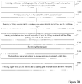
- Figure 20 illustrates an exemplary fabrication method to form a semiconductor structure consistent with the disclosed embodiments; and
- Figures 6-13 illustrate semiconductor structures corresponding to certain stages of the exemplary fabrication process.
- a substrate with certain structures may be formed (S101).
- Figure 6 illustrates a corresponding semiconductor structure.
- a substrate 100 including a plurality of initial fins 110 parallel to each other may be formed.
- the substrate 100 may provide a platform for subsequent fabrication processes to form the semiconductor structure.
- the initial fins 110 may be used to form fins, so as to form a FinFET.
- Forming the substrate 100 and the initial fins 110 may include: providing a base substrate; forming a patterned initial mask layer on the base substrate; and etching the base substrate with the patterned initial mask layer as an etching mask to form the substrate 100 and the initial fins 110.
- the base substrate may provide a platform for subsequent fabrication processes, and may be used to be etched to form the initial fins 110.
- the base substrate may be a monocrystalline silicon base substrate, thus the substrate 100 and the initial fins 110 may be made of monocrystalline silicon.
- the base substrate may be made of polysilicon, or amorphous silicon.
- the base substrate may also be made of germanium (Ge), gallium arsenide, or silicon germanium and other semiconductor materials thereof.
- the base substrate may also include a silicon structure having an epitaxial layer or on an epitaxial layer.
- the base substrate may include a substrate and a semiconductor layer on the substrate.
- the semiconductor layer may be formed on the substrate by a selective epitaxial deposition process.
- the substrate may include a silicon substrate, a germanium silicon substrate, a silicon carbide substrate, a silicon on insulator (SOI) substrate, a germanium on insulator (GOI) substrate, a glass substrate, or Group III-V compounds substrates, such as a gallium arsenide (GaAs) substrate, or a gallium nitride (GaN) substrate, etc.
- the semiconductor layer may be made of silicon, germanium, silicon carbide, or germanium silicon, etc.
- the materials of forming the substrate and the semiconductor layer are not limited.
- the substrate may be made of materials adapted to process requirements and easy integration, and the semiconductor layer may be made of materials adapted to forming the fin.
- the thickness of the semiconductor layer can be controlled by the epitaxial process, thus the height of the initial fin 110 can be precisely controlled.
- the patterned initial mask layer may be used to define the position and size of the initial fins 110.
- Forming the patterned initial mask layer may include: forming an initial mask material layer on the base substrate; forming a patterned layer on the initial mask material layer; and etching the initial mask material layer with the patterned layer as an etching mask until the surface of the base substrate is exposed to form the patterned initial mask layer.
- the initial mask layer may be made of silicon nitride.
- a buffer layer (not labeled) may be formed on the base substrate to improve the lattice mismatch problem between the initial mask layer and the base substrate.
- the buffer layer may be made of oxide.
- the patterned layer may be a patterned photoresist layer formed by a coating process and a photolithography process.
- the patterned layer may be formed by a multiple patterned mask process.
- the multiple patterned mask process may include a self-aligned double patterned (SaDP) process, a self-aligned triple patterned (SaTP) process, or a self-aligned double double patterned (SaDDP) process, etc.
- an isolation layer 120 may be formed between the adjacent fins 110.
- the isolation layer 120 may be used to electrically isolate the adjacent fins.
- the isolation layer 120 may be made of silicon oxide, silicon nitride, silicon oxynitride, low-K dielectric materials (dielectric constant is greater than or equal to 2.5 and is less than 3.9, such as porous silicon oxide, or porous silicon nitride), or ultra-low-K dielectric materials (dielectric constant is less than 2.5, such as porous SiCOH), etc.
- Forming the isolation layer 120 may include forming an isolation material layer to fill the space between the adjacent fins 110.
- the top surface of the isolation material layer may be above the top surfaces of the initial fins 110.
- Forming the isolation layer 120 may also include planarizing the isolation material layer until the top surfaces of the initial fins 110 are exposed.
- FCVD flowable chemical vapor deposition
- the planarization treatment may include a chemical mechanical polishing process. In one embodiment, the planarization treatment may also remove the initial mask layer formed on the initial fins 110 to expose the top surfaces of the initial fins 110.
- a liner oxide layer (not labeled) may be formed on the surfaces of the substrate 100 and the initial fins 110.
- the liner oxide layer may smooth the sharp corners on the surfaces of the substrate 100 and the initial fins 110, and act as a buffer layer between the subsequently formed film layer and the substrate 100 and the initial fins 110 to reduce the lattice mismatch thereof.
- the liner oxide layer may be formed by a chemical vapor deposition process, or a thermal oxidation process, etc.
- the damages may be repaired by performing an annealing process on the substrate 100 and the fins 110.
- a stop layer may be formed (S102).
- Figure 7 illustrates a corresponding semiconductor structure.
- a stop layer 131 may be formed on the initial fins 110 and the isolation layer 120.
- the stop layer 131 may be used to stop a subsequent planarization process.
- the stop layer 131 may also provide a process space for subsequently forming a sacrificial layer.
- the stop layer 131 may be made of silicon nitride.
- the stop layer 131 may be formed by a chemical vapor deposition process, a physical vapor deposition process, an atomic layer deposition process, or other film deposition processes.
- the stop layer 131 may also be used to define the thickness of the subsequently formed sacrificial layer. Therefore, the thickness of the stop layer 131 may be in a range of approximately 100 ⁇ - 2000 ⁇ .
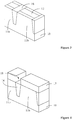
- a filling opening and a trench may be formed (S103).
- Figures 7-9 illustrate corresponding semiconductor structures.
- a filling opening 152 in the stop layer 131 and a trench 151 in the initial fins 110 and the isolation layer 120 may be formed by etching the stop layer 131, the initial fins 110, and the isolation layer 120.
- the extension direction of the trench 151 and the filling opening 152 may be perpendicular to the length direction of the initial fins 110.
- the filling opening 152 and the trench 151 formed by etching the stop layer 131, the initial fins 110, and the isolation layer 120 may provide process spaces for subsequently forming the sacrificial layer and an isolation structure.
- etching the , the initial fins 110, and the isolation layer 120 may include performing a dry etching process to etch the stop layer 131, the initial fins 110, and the isolation layer 120 to form the filling opening 152 and the trench 151.
- a stacked mask layer 132 having an etching opening 140 may be formed on the stop layer 131.
- the stacked mask layer 132 may be used as an etching mask when etching the stop layer 131 and the initial fins 110 to protect the stop layer from being etched.
- the etching opening 140 may be used to define the positions of the subsequently formed filling opening and trench.
- forming the stacked mask layer 132 may include: forming a filling layer 132a on the stop layer 131; forming a mask layer 132b on the filling layer 132a; forming a patterned layer 132c on the mask layer 132b; and forming the etching opening 140 in the patterned layer 132c.
- the bottom of the etching opening 140 may expose the mask layer 132b.
- the filling layer 132a may be used to fill the roughness of the surface of the stop layer 131.
- the filling layer 132a may be an organic dielectric layer (ODL).
- ODL organic dielectric layer
- the filling layer 132a may be formed on the stop layer 131 by a spin-on process.
- the mask layer 132b may be used as an etching mask to protect the film layer under the mask layer 132b.
- the mask layer 132b may be a SiO-based hard mask (SHB) layer.
- SHB SiO-based hard mask
- the mask layer 132b may be formed on the filling layer 132a by a chemical vapor deposition process, a physical vapor deposition process, an atomic layer deposition process, or other film deposition processes.
- the patterned layer 132c may be used to define the size and positions of the subsequently formed isolation structure and sacrificial layer.
- the patterned layer 132c may be a photoresist layer.
- the patterned layer 132c may be formed on the mask layer 132b by a coating process and a photolithography process.
- the etching opening 140 may be formed in the patterned layer 132c, and the bottom of the etching opening 140 may expose the surface of the SiO-based hard mask layer.
- the filling layer may also be an advanced patterning film (APF).
- APF advanced patterning film
- the mask layer may include a low temperature oxide layer and a bottom anti-reflection layer formed on the low temperature oxide layer; and the patterned layer may be a photoresist layer. The bottom of the etching opening may expose the bottom anti-reflection layer.
- the stacked mask layer 132 may be used as an etching mask to sequentially etch the mask layer 132b, the filling layer 132a, the stop layer 131, the initial fins 110, and the isolation layer 120, to form the filling opening 152 in the stop layer 131, and the trench 151 at the bottom of the filling opening 152 and penetrating through the filling opening 152.
- the filling opening 152 and the trench 151 may be formed by one same, single etching step and using the same mask for one time. Compared to the method of respectively forming the filling opening and the trench by two etching steps, the number of times for using the masks may be reduced, which is beneficial for simplifying the process and reducing the process cost.
- the method of forming the filling opening 152 and the trench 151 in the same, single etching step for one time can also avoid the overlay issue when multiple masks are used in conventional etching processes.
- the disclosed method is beneficial for reducing the process difficulty of forming the isolation structure and the sacrificial layer and improving the performance of the formed semiconductor structure.
- the stacked mask layer 132 may be removed to expose the stop layer 131.
- a tetramethylammonium hydroxide solution etching process may be performed to remove the stacked mask layer 132.
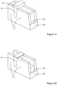
- an isolation structure and a sacrificial layer may be formed (S104).
- Figure 10 illustrates a corresponding semiconductor structure.
- the trench 151 (shown in Figure 9 ) and the filling opening 152 (shown in Figure 9 ) may be filled with a dielectric material.
- the top surface of the dielectric material may be coplanar with the surface of the stop layer 131.
- An isolation structure 161 may include the dielectric material filled in the trench 151, and a sacrificial layer 162 may include the dielectric material filled in the filling opening 152.
- the isolation structure 161 may divide the initial fins 110 into a plurality of fins 111 arranged along the length direction of the initial fins 110.
- the isolation structure 161 may be used to electrically isolate the adjacent fins 111 arranged along the length direction of the initial fins 110.
- the sacrificial layer 162 may be used to protect the isolation structure 161 when subsequently back-etching the isolation layer 120 to expose portions of sidewalls of the fins 111.
- the dielectric material may be silicon oxide. In certain embodiments, the dielectric material may be silicon nitride, silicon oxynitride, low-K dielectric materials (dielectric constant is greater than or equal to 2.5 and is less than 3.9), or ultra-low-K dielectric materials (dielectric constant is less than 2.5), etc.
- Forming the isolation structure 161 and the sacrificial layer 162 may include forming a dielectric material layer by filling the trench 151 and the filling opening 152 with the dielectric material. The top surface of the dielectric material layer may be above the top surface of the stop layer 131. Forming the isolation structure 161 and the sacrificial layer 162 may also include planarizing the dielectric material layer until the stop layer 131 is exposed, thus the top surface of the sacrificial layer 162 may be coplanar with the top surface of the stop layer 131.
- the dielectric material layer may be formed by a chemical vapor deposition process, a physical vapor deposition process, an atomic layer deposition process, or other film deposition processes.
- a chemical vapor deposition process As the device density increases, the distance between the adjacent fins 111 may decrease accordingly, thus the depth-to-width ratios of the trench 151 and the filling opening 152 may increase.
- FCVD flowable chemical vapor deposition
- a chemical mechanical polishing process may be used to perform the planarization process on the dielectric material layer.
- the stop layer may be removed (S105).
- Figure 11 illustrates a corresponding semiconductor structure.
- the stop layer 131 may be removed to expose the isolation layer 120.
- the process of removing the stop layer 131 to expose the top surface of the isolation layer 120 may provide a process surface for back-etching the isolation layer 120.
- a phosphoric acid etching process may be performed to remove the stop layer 131.
- the stop layer 131 may also cover the top surfaces of the fins 111, the top surfaces of the fins 111 may also be exposed while removing the stop layer 131 to expose the top surface of the isolation layer 120.
- the isolation layer may be back-etched (S106).
- Figure 12 illustrates a corresponding semiconductor structure.
- the isolation layer 120 may be back-etched to expose portions of sidewalls of the fins 111.
- the sacrificial layer 162 (shown in Figure 11 ) may be thinned when back-etching the isolation layer 120.
- the semiconductor structure is a FinFET
- back-etching the isolation layer 120 may be used to remove portions of thickness of the isolation layer 120 to expose portions of sidewalls of the fins 111.
- the subsequently formed gate structure may cover portions of sidewalls of the fins 111.
- a fluorine-containing gas may be used to back-etch the isolation layer 120.
- the fluorine-containing gas may include C 4 F 6 gas, or C 4 F 8 gas, etc.
- the sacrificial layer 162 may be thinned when back-etching the isolation layer 120. Because of the thinning of the sacrificial layer 162, the isolation structure 161 may be prevented from being lost when back-etching the isolation layer 120, so as to protect the isolation structure 161.
- a gate structure and a dummy gate structure may be formed (S107).
- Figure 13 illustrates a corresponding semiconductor structure.
- a gate structure 171 may be formed on the fins 111.
- the gate structure 171 may be across length portions of the fins 111, and cover portions of the top surface and sidewalls of each fin 111.
- a dummy gate structure 172 may be formed on the isolation structure 161 when forming the gate structure 171.
- forming the gate structure 171 and the dummy gate structure 172 may include: forming a gate material layer on the fins 111 and on the isolation structure 161; forming a gate patterned layer on the gate material layer, where the gate patterned layer may be used to define the size and positions of the gate structure 171 and the dummy gate structure 172; and etching the gate material layer with the gate patterned layer as an etching mask to form the gate structure 171 and the dummy gate structure 172.
- the gate structure 171 may be formed on the fins 111, and cover portions of the top surface and sidewalls of each fin 111.
- the dummy gate structure 172 may be formed on the isolation structure 161.
- the dummy gate structure 172 may be a dummy gate structure 172 in the single diffusion break process, and may be used to achieve isolation between the subsequently formed source region and drain region in the fins 111, so as to avoid the bridging issue between the formed source region and drain region.
- portions of thickness of the sacrificial layer 162 may be retained on the isolation structure 161.
- the dummy gate structure 172 may be formed on the remaining sacrificial layer 162 when forming the dummy gate structure 172.
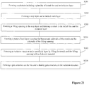
- Figure 21 illustrates another exemplary fabrication process to form a semiconductor structure consistent with the disclosed embodiments; and Figures 14-19 illustrate semiconductor structures corresponding to certain stages of the exemplary fabrication process.
- a substrate having a plurality of initial fins and an isolation layer may be formed (S201).
- Figure 14 illustrates a corresponding semiconductor structure.
- a substrate 200 including a plurality of initial fins 210 parallel to each other may be formed.
- An isolation layer 220 may be formed between the adjacent fins 210. Details of the substrate with the initial fins and the isolation layer can be referred to the above descriptions associated with Figure 6 , and are not repeated herein.
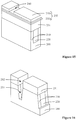
- a stop layer and a stacked mask layer may be formed (S202).
- Figure 15 illustrates a corresponding semiconductor structure.
- a stop layer 231 may be formed on the initial fins 210 and the isolation layer 220.
- the stop layer may be an advanced patterning film.
- the stop layer may be an organic dielectric layer.
- the stop layer 231 when forming the stop layer 231, may be the organic dielectric layer or the advanced patterning film.
- the method of forming the stop layer 231 by directly using the organic dielectric layer or the advanced patterning film may simplify the process steps and improve the process efficiency.
- a stacked mask layer 232 may be formed on the stop layer 231.
- forming the stacked mask layer 232 may include: forming a mask layer 232a on the stop layer 231; forming a patterned layer 232c on the mask layer 232a; and forming an etching opening 240 in the patterned layer 232c. The bottom of the etching opening 240 may expose the mask layer 232a.
- the stop layer may be the advanced patterning film.
- the mask layer 232a may include a low temperature oxide layer and a bottom anti-reflection layer formed on the low-temperature oxide layer.
- the patterned layer 232c may be a photoresist layer. The bottom of the etching opening may expose the bottom anti-reflection layer.
- the stop layer may be the organic dielectric layer.
- the mask layer may be a SiO-based hard mask layer; the patterned layer may be a photoresist layer; and the bottom of the etching opening may expose the surface of the SiO-based hard mask layer.
- a filling opening and a trench may be formed (S203).
- Figure 16 illustrates a corresponding semiconductor structure.
- the stop layer 231 and the initial fins 210 may be etched to form a filling opening 252 in the stop layer 231, and a trench 251 in the initial fins 210 and the isolation layer 220.
- the extension directions of the trench 251 and the filling opening 252 may be perpendicular to the length direction of the initial fin 210.
- the trench 251 and the filling opening 252 may be formed by sequentially etching the mask layer 232a, the stop layer 231, the initial fins 210, and the isolation layer 220 through the etching opening 240 (shown in Figure 15 ).
- the remaining stacked mask layer 232 may be removed to expose the stop layer 231.
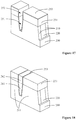
- a pattern fixed layer may be formed (S204).
- Figure 17 illustrates a corresponding semiconductor structure.
- a pattern fixed layer 253 may be formed after forming the filling opening 252 and the trench 251.
- the pattern fixed layer 253 may cover the bottom and sidewalls of the trench 251 and the sidewalls of the filling opening 252.
- the pattern fixed layer 253 may be used to fix the pattern shape of the trench 251 and the filling opening 252, thus the possibility of occurrence of the deformation of the stacked mask layer may be reduced.
- the pattern fixed layer 253 may be made of oxide.
- the pattern fixed layer 253 may be formed by an atomic layer deposition process. The method of forming the pattern fixed layer 253 by the atomic layer deposition process may improve the step coverage performance of the pattern fixed layer 253 and the accuracy of the pattern fixing of the pattern fixed layer 253 to the trench 251 and the filling opening 252.
- the thickness of the pattern fixed layer 253 may be in a range of approximately 100 ⁇ - 2000 ⁇ .
- the pattern fixed layer 253 may also cover the surface of the remaining stacked mask layer 232.
- the pattern fixed layer 253 may cover the top surface of the mask layer 232a.
- an isolation structure and a sacrificial layer may be formed (S205).
- Figure 18 illustrates a corresponding semiconductor structure.
- the trench 251 and the filling opening 252 may be filled with dielectric material to form an isolation structure 261 in the trench 251 (shown in Figure 17 ) and a sacrificial layer 262 in the filling opening 252 (shown in Figure 17 ).
- the isolation structure 261 may divide the initial fins 210 into a plurality of fins 211 arranged along the length direction of the initial fins 210.
- the dielectric material When filling the dielectric material, the dielectric material may also cover the top surface of the stop layer 231. After filling the trench 251 and the filling opening 252 with the dielectric material, the dielectric material may be planarized until the top surfaces of the remaining pattern fixed layer 253 and the remaining sacrificial layer 262 are coplanar with the top surface of the stop layer 231.
- a chemical mechanical polishing process may be used in the planarization treatment to remove portions of thickness of the dielectric material and the pattern fixed layer 253 to expose the top surface of the stop layer 231.
- a gate structure and a dummy gate structure may be formed (S206).
- Figure 19 illustrates a corresponding semiconductor structure.
- the stop layer 231 may be removed to expose the surface of the isolation layer 220.
- the stop layer 231 may be the advanced patterning film.
- a phosphoric acid etching process may be performed to remove the stop layer 231.
- the stop layer is the organic dielectric layer, a tetramethylammonium hydroxide solution etching process may be performed to remove the stop layer 231.
- the isolation layer 220 may be back-etched to expose portions of sidewalls of the fins 211.
- the sacrificial layer 262 (shown in Figure 18 ) may be thinned when back-etching the isolation layer 220.
- a gate structure 271 may be formed on the fins 211.
- the gate structure 271 may be across length portions of the fins 211, and may cover portions of the top surface and sidewalls of each fin 211.
- a dummy gate structure 272 may be formed on the isolation structure 261 when forming the gate structure 271.
- the steps of back-etching the isolation layer 220 and forming the gate structure 271 and the dummy gate structure 272 can be referred to the above-described embodiment, and are not repeated herein.
- Figure 19 illustrates a semiconductor structure consistent with the disclosed embodiments.
- the semiconductor structure may include a substrate 200 having a plurality of fins 211 parallel to each other and an isolation layer 220 formed on the substrate 200 between the adjacent fins 211 and perpendicular to a length direction of the fins 211.
- the top surface of the isolation layer 220 may be lower than the top surfaces of the fins 211, and the isolation layer 220 may expose portions of sidewalls of the fins 211.
- the semiconductor structure may also include an isolation structure 261 formed between the adjacent fins 211 arranged along the length direction of the fins 211. The extension direction of the isolation structure 261 may be perpendicular to the length direction of the fins 211.
- the semiconductor structure may include a pattern fixed layer 253 formed between the isolation structure 261 and the fins 211 as well as the substrate 200.
- the semiconductor structure may include a gate structure 271 formed on the fins 211.
- the gate structure 271 may be across length portions of the fins 211, and may cover portions of top surface and sidewalls of each fin 211.
- the semiconductor structure may include a dummy gate structure 272 formed on the isolation structure 261.
- the semiconductor substrate 200 may provide a platform for subsequent fabrication processes to form the semiconductor structure.
- the formed semiconductor structure may be a FinFET. Therefore, the plurality of fins 211 parallel to each other may be formed on the substrate 200.
- the substrate 200 and the fins 211 may be made of the same material. In one embodiment, the substrate 200 and the fins 211 may be made of monocrystalline silicon. In certain embodiments, the substrate 200 and the fins 211 may be made of polysilicon, or amorphous silicon. The substrate 200 and the fins 211 may also be made of germanium (Ge), gallium arsenide, or silicon germanium and other semiconductor materials thereof.
- the substrate and the fins may be made of different materials.
- the substrate may include a silicon substrate, a germanium silicon substrate, a silicon carbide substrate, a silicon on insulator (SOI) substrate, a germanium on insulator (GOI) substrate, a glass substrate, or Group III-V compounds substrates, such as a gallium arsenide (GaAs) substrate and a gallium nitride (GaN) substrate, etc.
- the fin may be made of silicon, germanium, silicon carbide, or germanium silicon, etc.
- the substrate may be made of materials adapted to process requirements and easy integration, and the semiconductor layer may be made of materials adapted to forming the fin.
- the isolation layer 220 may be used to electrically isolate the adjacent fins parallel to each other.
- the isolation layer 220 may be made of silicon oxide, silicon nitride, silicon oxynitride, low-K dielectric materials (dielectric constant is greater than or equal to 2.5 and is less than 3.9, such as porous silicon oxide, or porous silicon nitride), or ultra-low-K dielectric materials (dielectric constant is less than 2.5, such as porous SiCOH), etc.
- the isolation structure 261 may be used to electrically isolate the adjacent fins arranged along the length direction of the fins.
- the structure 261 may be made of silicon oxide, silicon nitride, silicon oxynitride, low-K dielectric materials (dielectric constant is greater than or equal to 2.5 and is less than 3.9), or ultra-low-K dielectric materials (dielectric constant is less than 2.5), etc.
- the pattern fixed layer 253 may be used to fix the pattern shape of a trench (not labeled) for forming the isolation structure 261 when forming the isolation structure 261.
- the pattern fixed layer 253 may be made of oxide, and may be formed by an atomic layer deposition process.
- the thickness of the pattern fixed layer 253 may be in a range of approximately 100 ⁇ - 2000 ⁇ .
- the dummy gate structure 272 may be a dummy gate structure 272 in the single diffusion break process.
- the dummy gate structure 272 may be used to achieve isolation between the subsequently formed source region and drain region in the adjacent fins 211 arranged along the length direction of the fins 211, so as to avoid the bridging issue between the formed source region and drain region.
- portions of thickness of a sacrificial layer may be retained on the isolation structure 261.
- the dummy gate structure 272 may be formed on the remaining sacrificial layer when forming the dummy gate structure 272.
- the filling opening in the stop layer and the trench in the initial fins may be formed by etching the stop layer and the initial fins.
- the isolation structure and the sacrificial layer may be formed by filling the filling opening and the trench with the dielectric material.
- the filling opening and the trench may be formed by one same, single etching step and using the same mask for one time. The number of times for using the masks may be reduced, which is beneficial for simplifying the process and reducing the process cost.
- the method of forming the filling opening and the trench in the same, single etching step for one time can also avoid the overlay issue when multiple masks are used in conventional etching processes.
- the disclosed method is beneficial for reducing the process difficulty of forming the isolation structure and the sacrificial layer, and improving the performance of the formed semiconductor structure.
- the disclosed method can be used to form FinFET devices having a critical dimension reduced to about 14 nm.
Landscapes
- Element Separation (AREA)
- Insulated Gate Type Field-Effect Transistor (AREA)
Applications Claiming Priority (1)
| Application Number | Priority Date | Filing Date | Title |
|---|---|---|---|
| CN201610711318.XA CN107768308B (zh) | 2016-08-23 | 2016-08-23 | 半导体结构及其形成方法 |
Publications (1)
| Publication Number | Publication Date |
|---|---|
| EP3288085A1 true EP3288085A1 (de) | 2018-02-28 |
Family
ID=59581773
Family Applications (1)
| Application Number | Title | Priority Date | Filing Date |
|---|---|---|---|
| EP17185681.8A Withdrawn EP3288085A1 (de) | 2016-08-23 | 2017-08-10 | Halbleiterstruktur und herstellungsverfahren dafür |
Country Status (3)
| Country | Link |
|---|---|
| US (1) | US20180061714A1 (de) |
| EP (1) | EP3288085A1 (de) |
| CN (1) | CN107768308B (de) |
Cited By (2)
| Publication number | Priority date | Publication date | Assignee | Title |
|---|---|---|---|---|
| EP3719836A3 (de) * | 2019-04-01 | 2020-12-09 | United Microelectronics Corp. | Halbleiterbauelement und verfahren zur herstellung davon |
| CN114121665A (zh) * | 2021-11-08 | 2022-03-01 | 长江存储科技有限责任公司 | 半导体器件的制作方法、半导体器件、存储器及存储系统 |
Families Citing this family (4)
| Publication number | Priority date | Publication date | Assignee | Title |
|---|---|---|---|---|
| TWI728139B (zh) | 2017-06-28 | 2021-05-21 | 聯華電子股份有限公司 | 半導體元件及其製作方法 |
| CN110875191A (zh) * | 2019-11-28 | 2020-03-10 | 上海华力集成电路制造有限公司 | 鳍式晶体管的制造方法 |
| US12525482B2 (en) * | 2021-08-27 | 2026-01-13 | Taiwan Semiconductor Manufacturing Company, Ltd. | Semiconductor devices and methods of manufacturing thereof |
| CN118571863B (zh) * | 2024-07-30 | 2024-11-12 | 合肥晶合集成电路股份有限公司 | 对准标记的制备方法及半导体结构 |
Citations (4)
| Publication number | Priority date | Publication date | Assignee | Title |
|---|---|---|---|---|
| US20120056263A1 (en) * | 2010-09-08 | 2012-03-08 | Samsung Electronics Co., Ltd. | Semiconductor trench isolation including polysilicon and nitride layers |
| US20140264572A1 (en) * | 2013-03-15 | 2014-09-18 | Sung-min Kim | Methods of forming semiconductor devices using hard mask layers |
| US20140353763A1 (en) * | 2013-06-03 | 2014-12-04 | Samsung Electronics Co., Ltd. | Semiconductor devices including fin-fets and methods of fabricating the same |
| US8916460B1 (en) * | 2013-08-07 | 2014-12-23 | Samsung Electronics Co., Ltd. | Semiconductor device and method for fabricating the same |
Family Cites Families (14)
| Publication number | Priority date | Publication date | Assignee | Title |
|---|---|---|---|---|
| JPH113936A (ja) * | 1997-06-13 | 1999-01-06 | Nec Corp | 半導体装置の製造方法 |
| US20100029057A1 (en) * | 2006-09-21 | 2010-02-04 | Jsr Corporation | Silicone resin composition and method of forming a trench isolation |
| US8659097B2 (en) * | 2012-01-16 | 2014-02-25 | Taiwan Semiconductor Manufacturing Company, Ltd. | Control fin heights in FinFET structures |
| KR102085525B1 (ko) * | 2013-11-27 | 2020-03-09 | 삼성전자 주식회사 | 반도체 장치 및 그 제조 방법 |
| KR102242580B1 (ko) * | 2014-04-23 | 2021-04-22 | 삼성전자주식회사 | 이미지 센서 및 이의 제조 방법 |
| US9171752B1 (en) * | 2014-08-12 | 2015-10-27 | Globalfoundries Inc. | Product comprised of FinFET devices with single diffusion break isolation structures, and methods of making such a product |
| US9123773B1 (en) * | 2014-08-15 | 2015-09-01 | Globalfoundries Inc. | T-shaped single diffusion barrier with single mask approach process flow |
| KR20160030794A (ko) * | 2014-09-11 | 2016-03-21 | 삼성전자주식회사 | 반도체 소자의 제조 방법 |
| US9373535B2 (en) * | 2014-10-16 | 2016-06-21 | Globalfoundries Inc. | T-shaped fin isolation region and methods of fabrication |
| KR102233073B1 (ko) * | 2014-12-03 | 2021-03-29 | 삼성전자주식회사 | 반도체 장치 및 그 제조 방법 |
| CN106711213B (zh) * | 2015-07-20 | 2021-02-26 | 联华电子股份有限公司 | 半导体元件及其制作方法 |
| US9997615B2 (en) * | 2015-11-30 | 2018-06-12 | Taiwan Semiconductor Manufacturing Co., Ltd. | Method for forming semiconductor structure with epitaxial growth structure |
| KR102402769B1 (ko) * | 2016-01-06 | 2022-05-26 | 삼성전자주식회사 | 반도체 장치 |
| CN107785315B (zh) * | 2016-08-26 | 2020-05-08 | 中芯国际集成电路制造(上海)有限公司 | 半导体结构的形成方法 |
-
2016
- 2016-08-23 CN CN201610711318.XA patent/CN107768308B/zh active Active
-
2017
- 2017-08-10 EP EP17185681.8A patent/EP3288085A1/de not_active Withdrawn
- 2017-08-16 US US15/678,830 patent/US20180061714A1/en not_active Abandoned
Patent Citations (4)
| Publication number | Priority date | Publication date | Assignee | Title |
|---|---|---|---|---|
| US20120056263A1 (en) * | 2010-09-08 | 2012-03-08 | Samsung Electronics Co., Ltd. | Semiconductor trench isolation including polysilicon and nitride layers |
| US20140264572A1 (en) * | 2013-03-15 | 2014-09-18 | Sung-min Kim | Methods of forming semiconductor devices using hard mask layers |
| US20140353763A1 (en) * | 2013-06-03 | 2014-12-04 | Samsung Electronics Co., Ltd. | Semiconductor devices including fin-fets and methods of fabricating the same |
| US8916460B1 (en) * | 2013-08-07 | 2014-12-23 | Samsung Electronics Co., Ltd. | Semiconductor device and method for fabricating the same |
Cited By (8)
| Publication number | Priority date | Publication date | Assignee | Title |
|---|---|---|---|---|
| EP3719836A3 (de) * | 2019-04-01 | 2020-12-09 | United Microelectronics Corp. | Halbleiterbauelement und verfahren zur herstellung davon |
| US10943993B2 (en) | 2019-04-01 | 2021-03-09 | United Microelectronics Corp. | Semiconductor device and method for fabricating the same |
| US11527638B2 (en) | 2019-04-01 | 2022-12-13 | United Microelectronics Corp. | Semiconductor device and method for fabricating the same |
| US11581422B2 (en) | 2019-04-01 | 2023-02-14 | United Microelectronics Corp. | Semiconductor device and method for fabricating the same |
| US12100750B2 (en) | 2019-04-01 | 2024-09-24 | United Microelectronics Corp. | Semiconductor device and method for fabricating the same |
| US12125900B2 (en) | 2019-04-01 | 2024-10-22 | United Microelectronics Corp. | Semiconductor device and method for fabricating the same |
| CN114121665A (zh) * | 2021-11-08 | 2022-03-01 | 长江存储科技有限责任公司 | 半导体器件的制作方法、半导体器件、存储器及存储系统 |
| CN114121665B (zh) * | 2021-11-08 | 2024-02-23 | 长江存储科技有限责任公司 | 半导体器件的制作方法、半导体器件、存储器及存储系统 |
Also Published As
| Publication number | Publication date |
|---|---|
| CN107768308B (zh) | 2020-10-09 |
| CN107768308A (zh) | 2018-03-06 |
| US20180061714A1 (en) | 2018-03-01 |
Similar Documents
| Publication | Publication Date | Title |
|---|---|---|
| US10483169B2 (en) | FinFET cut-last process using oxide trench fill | |
| CN111490092B (zh) | 半导体结构及其形成方法 | |
| US9704974B2 (en) | Process of manufacturing Fin-FET device | |
| US10714613B2 (en) | Semiconductor device | |
| EP3288085A1 (de) | Halbleiterstruktur und herstellungsverfahren dafür | |
| US8936986B2 (en) | Methods of forming finfet devices with a shared gate structure | |
| CN110323267A (zh) | 半导体结构及其形成方法 | |
| US9117907B2 (en) | Semiconductor device | |
| US11742414B2 (en) | Semiconductor device with fins | |
| US12463049B2 (en) | Semiconductor structure and forming method thereof | |
| KR20160088220A (ko) | 반도체 소자 및 그 제조 방법 | |
| EP3288070B1 (de) | Herstellungsverfahren für halbleiterstruktur | |
| CN115360145A (zh) | 一种半导体结构及其制造方法 | |
| CN107134451A (zh) | 鳍型场效晶体管及其制作方法 | |
| EP3285298A1 (de) | Schutzstruktur gegen elektrostatische entladungen und herstellungsverfahren dafür | |
| CN110854194B (zh) | 半导体结构及其形成方法 | |
| CN107452680B (zh) | 半导体装置及其制造方法 | |
| CN108122762B (zh) | 半导体结构及其形成方法 | |
| CN112117192B (zh) | 半导体结构的形成方法 | |
| CN113937164B (zh) | 半导体结构的形成方法 | |
| CN107731917B (zh) | 半导体结构的形成方法 | |
| CN112768408A (zh) | 鳍式场效应晶体管的形成方法 | |
| US20260068286A1 (en) | Nanostructure field-effect transistor device and methods of forming | |
| CN108022843B (zh) | 半导体结构的形成方法 | |
| CN114765131B (zh) | 半导体结构的形成方法 |
Legal Events
| Date | Code | Title | Description |
|---|---|---|---|
| PUAI | Public reference made under article 153(3) epc to a published international application that has entered the european phase |
Free format text: ORIGINAL CODE: 0009012 |
|
| STAA | Information on the status of an ep patent application or granted ep patent |
Free format text: STATUS: THE APPLICATION HAS BEEN PUBLISHED |
|
| AK | Designated contracting states |
Kind code of ref document: A1 Designated state(s): AL AT BE BG CH CY CZ DE DK EE ES FI FR GB GR HR HU IE IS IT LI LT LU LV MC MK MT NL NO PL PT RO RS SE SI SK SM TR |
|
| AX | Request for extension of the european patent |
Extension state: BA ME |
|
| STAA | Information on the status of an ep patent application or granted ep patent |
Free format text: STATUS: REQUEST FOR EXAMINATION WAS MADE |
|
| 17P | Request for examination filed |
Effective date: 20180803 |
|
| RBV | Designated contracting states (corrected) |
Designated state(s): AL AT BE BG CH CY CZ DE DK EE ES FI FR GB GR HR HU IE IS IT LI LT LU LV MC MK MT NL NO PL PT RO RS SE SI SK SM TR |
|
| RAP1 | Party data changed (applicant data changed or rights of an application transferred) |
Owner name: SEMICONDUCTOR MANUFACTURING INTERNATIONAL (SHANGHA Owner name: SEMICONDUCTOR MANUFACTURING INTERNATIONAL (BEIJING |
|
| STAA | Information on the status of an ep patent application or granted ep patent |
Free format text: STATUS: EXAMINATION IS IN PROGRESS |
|
| 17Q | First examination report despatched |
Effective date: 20200624 |
|
| STAA | Information on the status of an ep patent application or granted ep patent |
Free format text: STATUS: THE APPLICATION IS DEEMED TO BE WITHDRAWN |
|
| 18D | Application deemed to be withdrawn |
Effective date: 20201105 |