EP3289407B1 - Modulateur de réflexion indépendant de la polarisation - Google Patents
Modulateur de réflexion indépendant de la polarisation Download PDFInfo
- Publication number
- EP3289407B1 EP3289407B1 EP16795788.5A EP16795788A EP3289407B1 EP 3289407 B1 EP3289407 B1 EP 3289407B1 EP 16795788 A EP16795788 A EP 16795788A EP 3289407 B1 EP3289407 B1 EP 3289407B1
- Authority
- EP
- European Patent Office
- Prior art keywords
- optical
- polarization
- modulator
- light path
- pirm
- Prior art date
- Legal status (The legal status is an assumption and is not a legal conclusion. Google has not performed a legal analysis and makes no representation as to the accuracy of the status listed.)
- Active
Links
Images







Classifications
-
- H—ELECTRICITY
- H04—ELECTRIC COMMUNICATION TECHNIQUE
- H04J—MULTIPLEX COMMUNICATION
- H04J14/00—Optical multiplex systems
- H04J14/06—Polarisation multiplex systems
-
- G—PHYSICS
- G02—OPTICS
- G02F—OPTICAL DEVICES OR ARRANGEMENTS FOR THE CONTROL OF LIGHT BY MODIFICATION OF THE OPTICAL PROPERTIES OF THE MEDIA OF THE ELEMENTS INVOLVED THEREIN; NON-LINEAR OPTICS; FREQUENCY-CHANGING OF LIGHT; OPTICAL LOGIC ELEMENTS; OPTICAL ANALOGUE/DIGITAL CONVERTERS
- G02F1/00—Devices or arrangements for the control of the intensity, colour, phase, polarisation or direction of light arriving from an independent light source, e.g. switching, gating or modulating; Non-linear optics
- G02F1/01—Devices or arrangements for the control of the intensity, colour, phase, polarisation or direction of light arriving from an independent light source, e.g. switching, gating or modulating; Non-linear optics for the control of the intensity, phase, polarisation or colour
- G02F1/21—Devices or arrangements for the control of the intensity, colour, phase, polarisation or direction of light arriving from an independent light source, e.g. switching, gating or modulating; Non-linear optics for the control of the intensity, phase, polarisation or colour by interference
-
- H—ELECTRICITY
- H04—ELECTRIC COMMUNICATION TECHNIQUE
- H04B—TRANSMISSION
- H04B10/00—Transmission systems employing electromagnetic waves other than radio-waves, e.g. infrared, visible or ultraviolet light, or employing corpuscular radiation, e.g. quantum communication
- H04B10/25—Arrangements specific to fibre transmission
- H04B10/2575—Radio-over-fibre, e.g. radio frequency signal modulated onto an optical carrier
-
- H—ELECTRICITY
- H04—ELECTRIC COMMUNICATION TECHNIQUE
- H04B—TRANSMISSION
- H04B10/00—Transmission systems employing electromagnetic waves other than radio-waves, e.g. infrared, visible or ultraviolet light, or employing corpuscular radiation, e.g. quantum communication
- H04B10/27—Arrangements for networking
- H04B10/272—Star-type networks or tree-type networks
-
- H—ELECTRICITY
- H04—ELECTRIC COMMUNICATION TECHNIQUE
- H04B—TRANSMISSION
- H04B10/00—Transmission systems employing electromagnetic waves other than radio-waves, e.g. infrared, visible or ultraviolet light, or employing corpuscular radiation, e.g. quantum communication
- H04B10/50—Transmitters
- H04B10/501—Structural aspects
- H04B10/503—Laser transmitters
- H04B10/505—Laser transmitters using external modulation
-
- G—PHYSICS
- G02—OPTICS
- G02F—OPTICAL DEVICES OR ARRANGEMENTS FOR THE CONTROL OF LIGHT BY MODIFICATION OF THE OPTICAL PROPERTIES OF THE MEDIA OF THE ELEMENTS INVOLVED THEREIN; NON-LINEAR OPTICS; FREQUENCY-CHANGING OF LIGHT; OPTICAL LOGIC ELEMENTS; OPTICAL ANALOGUE/DIGITAL CONVERTERS
- G02F1/00—Devices or arrangements for the control of the intensity, colour, phase, polarisation or direction of light arriving from an independent light source, e.g. switching, gating or modulating; Non-linear optics
- G02F1/01—Devices or arrangements for the control of the intensity, colour, phase, polarisation or direction of light arriving from an independent light source, e.g. switching, gating or modulating; Non-linear optics for the control of the intensity, phase, polarisation or colour
- G02F1/21—Devices or arrangements for the control of the intensity, colour, phase, polarisation or direction of light arriving from an independent light source, e.g. switching, gating or modulating; Non-linear optics for the control of the intensity, phase, polarisation or colour by interference
- G02F1/211—Sagnac type
-
- G—PHYSICS
- G02—OPTICS
- G02F—OPTICAL DEVICES OR ARRANGEMENTS FOR THE CONTROL OF LIGHT BY MODIFICATION OF THE OPTICAL PROPERTIES OF THE MEDIA OF THE ELEMENTS INVOLVED THEREIN; NON-LINEAR OPTICS; FREQUENCY-CHANGING OF LIGHT; OPTICAL LOGIC ELEMENTS; OPTICAL ANALOGUE/DIGITAL CONVERTERS
- G02F2203/00—Function characteristic
- G02F2203/06—Polarisation independent
-
- H—ELECTRICITY
- H04—ELECTRIC COMMUNICATION TECHNIQUE
- H04J—MULTIPLEX COMMUNICATION
- H04J14/00—Optical multiplex systems
- H04J14/02—Wavelength-division multiplex systems
- H04J14/0227—Operation, administration, maintenance or provisioning [OAMP] of WDM networks, e.g. media access, routing or wavelength allocation
- H04J14/0241—Wavelength allocation for communications one-to-one, e.g. unicasting wavelengths
- H04J14/0242—Wavelength allocation for communications one-to-one, e.g. unicasting wavelengths in WDM-PON
- H04J2014/0253—Allocation of downstream wavelengths for upstream transmission
Definitions
- carrier distribution has been considered as a promising scheme in realizing a low-cost light source for uplink signal.
- an optical carrier signal is delivered from an optical source positioning in a central office to a remote device.
- the remote device then modulates uplink data onto the received optical carrier signal, and sends the modulated carrier signal back to the central office.
- current modulators employed in such systems are either temperature sensitive or only operate at a relatively low speed to avoid overheating.
- carrier distribution is not feasible if the remote device is uncooled and is therefore exposed to temperatures in excess of 85 degrees Celsius (°C) and/or if the application requires high speed operation. In such cases, conventional modulators are unable to properly modulate a usable uplink signal.
- WO 94/25883 A1 discloses an apparatus and method for converting a signal of arbitrary polarization to one of preselected polarization, e.g. for use by a sensor, transducer, etc.
- a signal splitter divides the input signal into its orthogonal linearly polarized components, and launches the components from a pair of output ports.
- the signals counterpropagate to the opposite port, and, while couterpropagating, are rotated into the same linear polarization state.
- the rotation is done by a pair of complementary 45 degree Faraday rotators; in another, by one 90 degree rotator.
- the signal is recombined at the splitter in the initial state of polarization that in which the signal initially entered the splitter; in the latter, the recombined signal is of orthoconjugate polarization to the input signal.
- WO 01/35539 A2 discloses Systems and techniques for transmitting and processing an electrical signal through an opto-electronic system with an optical Brillouin amplifier (see Abstract).
- a photonic RF link may be configured to achieve a number of signal processing operations in the optical domain, including frequency up or down conversion and signal amplification. The processing operations in the optical domain may be insensitive to the polarization state of light and substantially free of the fiber dispersion effect after transmission through a fiber link.
- Such a photonic RF link may also use low loss and less expensive optical phase modulators to avoid modulator bias problems in some optical intensity modulators.
- the disclosure includes an apparatus as defined in claim 1.
- CRANs cloud radio access networks
- traffic rate requirements may necessitate the use of fiber connections between remote radio units (RRUs) and baseband units (BBUs).
- RRUs remote radio units
- BBUs baseband units
- an optical transponder may be placed at a tower which is connected to the radio unit via common public radio interface (CPRI).
- CPRI common public radio interface
- the transponder may be subjected to high temperatures in excess of 85° C.
- uncooled lasers may not operate properly and/or may not provide sufficient power budget, particularly at high-speed modulation rates, for example, greater than or equal to 25 gigabits per second (Gbps).
- Gbps gigabits per second
- Cooling lasers using thermoelectric cooling (TEC) significantly increase power consumption.
- optical modulators such as Mach-Zehnder modulators
- PIRM polarization independent reflective modulator
- the PIRM employs a polarization beam splitter/combiner to split the incoming optical carrier into two perpendicular polarization components, sometimes referred to herein as transverse electric (TE) and transverse magnetic (TM) components, and forwards each of the polarization components along a different light path.
- One of the polarization components is then rotated to be parallel to the other component.
- the TM component is rotated, resulting in a second TE component.
- both polarization components share the same polarization, which allows a polarization sensitive modulator to operate on both components.
- the two polarization components are input into an optical modulator from opposite ends for substantially simultaneous modulation.
- PIRMs may be coupled to a multiplexer to allow each PIRM to operate on a different wavelength ( ⁇ ), allowing the PIRMs to support wavelength division multiplexing.
- the PIRM(s) are positioned in one or more RRUs, each corresponding to a BBU comprising the optical source (e.g. laser).
- the PIRMs may be positioned in server rack, for example in the servers or in a top of rack (ToR) element.
- PIRMs may also be positioned in end of row (EOR) switches, which allows a single optical source/laser to provide carriers for a plurality of sever rows.
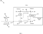
- FIG. 1 is a schematic diagram of an embodiment of a polarization independent reflective modulator (PIRM) 100.
- the PIRM 100 comprises a polarization beam splitter (PBS) 155 coupled to a modulator 159 via a light path 156 and a light path 158, sometimes generally referred to herein as a first/second light path.
- Reflectors 151, 152, and 153 are positioned along the light paths 156 and 158 to control the direction of light traversing the light paths 156 and 158.
- the PIRM 100 further comprises an optical input 147 for receiving an optical carrier 141 and transmitting an uplink signal 143 over an optical medium, such as an optical fiber, etc.
- the PBS 155 may be any device configured to split an optical carrier into two polarized light beams and output the polarized light beams along light paths 158 (in a clockwise direction) and 156 (in a counter-clockwise (CCW) direction), respectively. Specific examples of PBS 155 are discussed further in various embodiments below.
- the PBS 155 receives an optical carrier 141 via an optical input 147, which may be a port, an optical waveguide, etc.
- the optical carrier 141 may be received from a remote apparatus comprising a continuous wavelength laser or similar optical source.
- the optical carrier 141 may be linearly polarized upon leaving the remote device, but may become elliptically polarized during transmission to the PIRM.
- the optical carrier may comprise a single optical component, such as a TE polarization, but portions of the optical carrier may rotate into a TM polarization when traversing an optical fiber.
- the PBS 155 sends the light beam of the received optical carrier 141 containing the TE polarization portion via light path 156.
- the PBS 155 sends the light beam of the received optical carrier 141 containing the TM polarization portion via light path 158.
- light in clockwise direction contains whatever portion of the optical carrier that comprises a polarization that is perpendicular to light beam in CCW direction.
- the light paths 156 and 158 may comprise any medium with a refractive index suitable for communicating an optical signal, for example an optical waveguide, glass, air, etc.
- a polarization rotator (PR) 157 is positioned along light path 158.
- PR 157 may be any device configured to rotate the polarization of a polarized light beam by a specified angle, such as a Faraday rotator or a mode converter. Specifically, PR 157 rotates the polarization of light beam in the clockwise direction so that the light beam becomes polarized in parallel with the light beam in CCW direction (e.g. a 90 degree rotation).
- PR 157 converts the TM polarization of light beam in clockwise direction into a TE polarization so that the light in both directions comprise the same polarization.
- the PIRM 100 comprises reflectors 151, 152, and 153.
- the reflectors 151-153 may be any materials/devices with refractive index sufficient to alter the direction of light beam in clockwise and CCW directions along the light paths 156 and 158, as shown.
- Modulator 159 may be any device capable of modulating an electrical signal onto an optical carrier. Specifically, modulator 159 is a high speed lumped modulator where the modulator active length may be less than 2 millimeters (mm).
- Modulator 159 may be implemented as any silicon waveguide based modulator, a single lumped modulator, a Mach-Zehnder modulator (MZM), an Inphase Quadrature (IQ) modulator, an electro-absorption modulator, a micro-ring resonator based modulator, etc.
- Modulator 159 comprises a proximate end and a distal end coupled to light path 156 and light path 158, respectively.
- Modulator 159 is configured to receive the light beam in CCW direction at the proximate end and receive the light beam in clockwise direction at the distal end. As light beams in both directions pass through modulator 159, the modulator 159 substantially simultaneously modulates the electrical signal onto both light beams.
- Modulator 159 may be selected to be temperature insensitive and polarization sensitive. However, because the TM component has been rotated into a TE polarization by PR 157, both light beams share the same polarization. Accordingly, modulator 159 can modulate both light beams despite the light beams being received from opposite directions. To ensure the same portion of optical carrier 141 is substantially simultaneously modulated by modulator 159 (e.g. no signal skews), light paths 156 and 158 should be approximately the same length, placing the modulator 159 in the center of the optical circuit. Modulator 159 position may vary slightly (e.g. 0.5 picoseconds (ps), 1 ps, etc. difference between light path travel times) without significantly impacting modulation, as shown in FIG. 12 below.
- ps picoseconds
- 1 ps etc. difference between light path travel times
- Modulated light beams exit the modulator 159 from opposite ends, such that the modulated light beam in the CCW direction leaves the distal end and the modulated light beam in clockwise direction leaves the proximate end.
- the modulated light beam in the clockwise direction continues clockwise around the optical circuit via light path 156 and the modulated light beam in the CCW direction continues counter-clockwise around the optical circuit via light path 158.
- the modulated light beams in both directions are both received back at PBS 155 and combined into a combined modulated optical signal 143, which is then transmitted upstream across the same fiber transporting the optical carrier 141.
- PIRM 100 By employing the optical circuit of PIRM 100, the dependence of polarization on incoming optical carrier is eliminated. Accordingly, PIRM 100 allows the laser/optical source to be moved to a remote apparatus while allowing modulation to occur in a high temperature environment by a temperature insensitive modulator. Further, it should be noted that first component, second component, TM, and TE are employed herein as labels for purposes of discussion, but may be alternated in some embodiments without affecting the operation of PIRM 100. Further, PR 157 may instead be positioned in light path 156 with the PBS 155 TM polarization output connected to path 156, but with no change in the combined modulated signal 143 output from the PIRM.
- the modulator 159 can be designed to be located at the middle of an optical path comprising both light path 156 and light path 158. Practical fabrication may have some tolerance.
- E out is the PIRM 100 output optical field as a function of time (t)
- E in is the amplitude of the PIRM 100 input optical field
- f(t) is the modulation waveform function of modulated data over time
- T is the delay of the PIRM 100 optical path (e.g.
- Equation 3 shows that the total output of PIRM 100 is independent to the polarization state of the incoming optical carrier.
- FIG. 2 is a schematic diagram of an embodiment of a cloud radio access network (CRAN) 200 configured to employ a PIRM 221, which may be similar to PIRM 100 or any other PIRM embodiment disclosed herein.
- CRAN 200 comprises a pool of BBUs each comprising a BBU transceiver (Tx/Rx) 211.
- Each BBU Tx/Rx 211 is coupled to a corresponding RRU 220, for example, via one or more optical fibers.
- Each RRU 220 comprises a wireless Tx/Rx 225, a PIRM 221, and a downlink receiver (Rx) 223.
- Each RRU 220 communicates with mobile nodes (MNs) via a wireless interface, such as an Long Term Evolution (LTE) interface, LTE advanced interface, etc., across the wireless Tx/Rx 225.
- MNs mobile nodes
- Each BBU Tx/Rx 211 sends an optical downlink signal 245 to the corresponding downlink Rx 223 for transmission to the corresponding MN.
- the downlink signal 245 is converted to electrical downlink data 235 and transmitted to the MN via wireless Tx/Rx 225.
- the MN transmits corresponding uplink data 233 via wireless Tx/Rx 225.
- RRU 220 does not comprise an optical source (e.g., a laser, Light Emitting Diode (LED), etc.).
- the BBU Tx/Rx 211 transmits an optical uplink carrier 241 downstream to the RRU 220.
- the RRU 220 employs the PIRM 221 to modulate the uplink data 233 from the MN onto the uplink carrier 241 to create an optical uplink signal 243.
- the uplink signal 243 is then returned to the BBU Tx/Rx 211 via the optical fiber, for example across the same fiber as the uplink carrier 241.
- the uplink signal 243 can then be separated from the uplink carrier 241 at the BBU Tx/Rx 211.
- a BBU pool is any grouping of BBUs, for example positioned in a wireless base station, equipment room, etc., for processing baseband signals.
- Each BBU may comprise one or more BBU Tx/Rxs 211, each of which is responsible for communicating with a corresponding RRU 220.
- the BBU Tx/Rxs 211 each comprise one or more optical sources, such as continuous wave lasers. The optical sources transmit polarized optical carriers toward the RRUs 220.
- the BBU Tx/Rxs 211 each comprise modulators to modulate a downlink signal 245 onto a downlink optical carrier provided by a downlink optical source.
- the BBU Tx/Rxs 211 also each comprise a receiver to receive the uplink signal and an optical splitter/combiner or optical circulator to separate the uplink signal 243 from the uplink carrier 241 (provided by an uplink optical source) transmitted over the optical fiber.
- PIRMs may also be employed on the BBUs to eliminate the polarization dependence of the optical carriers.
- the BBU pool may be arranged in a star-topology as shown such that the CRAN 200 comprises a BBU pool and multiple RRUs 220.
- the star-topology based CRAN 200 can be extended to a CRAN 200 with tree-topology or other architectures.
- a tree-topology may save fiber length but may suffer from signal loss due to the introduction of power splitters in the optical link.
- the RRUs 220 each comprise a wireless Tx/Rx 225, which may be any antenna or antenna array configured to wirelessly communicate with MNs via an LTE, LTE advanced, or other wireless system.
- RRUs 220 each further comprise a downlink Rx 223 coupled to the wireless Tx/Rx 225.
- the downlink Rx 223 may be any optical receiver configured to detect an optical signal received over a fiber, for example a Positive-Negative (P-N) junction, a photodiode, or similar structure.
- the RRUs 220 each may further comprise processor(s), memory, cache, etc. to control the wireless Tx/Rx 225 and cause the downlink data 235 from the downlink Rx 223 to be transmitted on specified wireless bands at specified times.
- the RRU 220 does not comprise an optical source, so the uplink carrier 241 is provided by the BBU Tx/Rx 211.
- the PIRM 221 modulates uplink data 233 from the wireless Tx/Rx 225 onto the uplink carrier 241 to create the uplink signal 243, which is returned to the BBU Tx/Rx 211.
- the fiber length between the BBU Tx/Rx 211 and the RRU 220 can range from tens of meters to tens of kilometers resulting in significant random alteration of the polarization of the uplink carrier while traversing the fiber.
- the PIRM 221 eliminates the polarization dependence and modulates the uplink carrier 241 regardless of temperature.
- the RRU 220 can be located on a tower in an uncooled environment. Further, the RRU 220 can be produced more cheaply as no laser or similar optical source is required.
- FIG. 3 is a schematic diagram of an embodiment of a CRAN 300 configured to employ wavelength division multiplexing via a plurality of PIRMs 321, which may be substantially similar to PIRM 100 or any other PIRM embodiment disclosed herein.
- CRAN 300 comprises a BBU 311 and an RRU 320, which may be substantially similar to a BBU Tx/Rxs 211 and an RRU 220, respectively, but are configured to communicate via wavelength division multiplexing (WDM).
- WDM wavelength division multiplexing
- the BBU 311 comprises a desired number (N) of continuous wavelength (CW) lasers 313.
- Each CW laser 313 is an optical source and transmits an uplink carrier 341 comprising a wavelength ( ⁇ ), resulting in uplink carriers 341 of ⁇ 1 to ⁇ N .
- BBU 311 further comprises an optical multiplexer (Mux) 314, which may be any device capable of combining a plurality of optical carriers/signals of different wavelength into a single fiber and/or capable of splitting multiple wavelengths from a single fiber into a plurality of fibers according to wavelength.
- Mux 314 is configured to multiplex uplink carriers 341 of ⁇ 1 to ⁇ N into a single fiber for transmission to RRU 320.
- RRU 320 comprises a Mux 327 that substantially similar to Mux 314 and is configured to separate the multiplexed carriers 341 ⁇ 1 - ⁇ N to different ports based on wavelength.
- RRU 320 further comprises N PIRMs 321 coupled to Mux 327.
- Each PIRM 321 is substantially similar to PIRM 221, but is allocated to a particular wavelength.
- RRU 320 receives N uplink data 333 signals, which are substantially similar to uplink data 233 signals.
- Each uplink data 333 signal is modulated to a specified uplink carrier 341 ⁇ at a corresponding PIRM 321 resulting in uplink signals 343 ⁇ 1 - ⁇ N .
- Uplink signals 343 are combined by the Mux 327 into a single uplink port for transmission back across the fiber to BBU 311.
- the BBU 311 further comprises an optical coupler (OC) 318 coupled to Mux 314.
- the OC 318 may be any device capable of separating/combining the uplink carriers 341 headed in the downstream direction from/with the uplink signals 343 headed in the upstream direction across a single fiber.
- an OC 318 may be an optical coupler, an optical circulator, or other optical splitting/combining device.
- the OC 318 is also coupled to a Mux 316. The OC 318 forwards the combined uplink carriers 341 from Mux 314 in toward the RRU 320 and forwards the combined uplink signals 343 from the RRU 320 toward Mux 316.
- Mux 316 is substantially similar to Mux 314 and is configured to split the combined uplink signals 343 into individual signals before forwarding each uplink signal 343 to a corresponding uplink Rx 315.
- the uplink Rxs 315 are each substantially similar to a downlink Rx 223, but are configured to receive and interpret a corresponding uplink signal 343 at a corresponding wavelength. Accordingly, N uplink Rxs 315 are employed to receive uplink signals 343 ⁇ 1 - ⁇ N .
- optical amplifier may be placed between the OC 318 and Mux 316 or between OC 318 and the transmission fiber.
- optical amplifiers include, but are not limited to, semiconductor optical amplifiers (SOAs), reflective-type SOAs (RSOAs), and erbium doped finer amplifiers (EDFAs).
- SOAs semiconductor optical amplifiers
- RSOAs reflective-type SOAs
- EDFAs erbium doped finer amplifiers
- wavelength division multiplexing may be in different forms, such as coarse WDM, local area network (LAN)-WDM, or dense WDM, and may be operated at different wavelength bands, for example, the O-band, C-band, and L-band optical bands.
- LAN local area network
- L-band optical bands for example, the O-band, C-band, and L-band optical bands.
- a downlink channel may be configured in a similar manner to the uplink channel (e.g.
- an RRU 320 can employ wavelength division multiplexing to communicate a plurality of uplink signals without comprising a laser or other optical source.
- the RRU 320 can be produced cheaply and operate in a high temperature environment while employing a single fiber for a plurality of uplink signals 343.
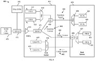
- FIG. 4 is a schematic diagram of an embodiment of a datacenter network 400 configured to employ PIRMs 413 and 421, which may be substantially similar to PIRM 100 or any other PIRM embodiment disclosed herein.
- Datacenter network 400 comprises a plurality of rack servers 420, which are hardware devices that provide services to clients, for example by providing applications, operating software, virtualization, cloud computing, etc.
- Each rack of rack servers 420 may be interconnected by a Top of Rack (TOR) switch.
- the TOR switches/Rack servers may be organized in rows, such that each row is connected to an EOR switch 411 or 470.
- the EOR switches 411 or 470 are then coupled to a core network, allowing the rack servers 420 to communicate with clients via the EORs 411/470 and the core network.
- EOR switches 411 and 470 and rack servers 420 each comprise PIRMs 413 and 421, respectively, allowing WDM CW lasers 473 to provide optical carriers for a plurality of servers, a plurality of server racks, and/or a plurality of server rows in the datacenter network 400.
- the WDM Lasers 473 may be any optical light source that transmits a plurality of optical carriers at a plurality of wavelengths, and may be substantially similar to CW lasers 313.
- Optical carriers from the WDM Lasers 473 are forwarded to a splitter 471, which is any device configured to split an optical carrier into multiple portions, for example into multiple copies of the same group of optical carriers with reduced power/luminance.
- the optical carriers exit the splitter 471 and are forwarded to EOR switch 411 and other EOR switches 470, which are substantially similar to EOR switch 411, but are not shown in detail for clarity of discussion.
- EOR switch 411 is any device capable of connecting other devices by performing packet switching across an optical network.
- the optical carriers are received at the EOR switch 411 and forwarded through an EDFA 419 to amplify the power/luminance of the optical carriers.
- other amplifiers such as SOAs may be employed in addition to or in place of the EDFA 419.
- the amplified optical carriers are forwarded through an additional splitter 471 resulting in a set of uplink carriers 441 and a set of downlink carriers 444.
- the uplink carriers 441 are forwarded to the rack servers 420 and the downlink carriers 444 are forwarded for modulation.
- EOR switch 411 comprises PIRMs 413, which are similar to PIRMs 321 and are interconnected by a Mux 414, which is substantially similar to Mux 314.
- EOR switch 411 further comprises an OC 418, which is substantially similar to OC 318.
- the downlink carriers 444 pass through the OC 418 and are forwarded to Mux 414.
- Mux 414 splits the downlink carriers 444 into N carriers by wavelength and forwards them to the corresponding PIRMs 413 for modulation.
- PIRMs 413 modulate a plurality of downlink data onto the downlink carriers 444 to create downlink signals 445, which are then combined by the Mux 414 for transmission to the rack servers 420 via OC 418.
- the rack servers 420 comprise a Mux 429 and downlink (DL) Rxs 425, which are substantially similar to Mux 316 and uplink Rxs 315, respectively, but configured to convey downlink signals 445.
- Mux 429 splits the downlink signals 445 by wavelength and forwards them to the DL Rxs 425 to be received and converted to electrical downlink data.
- the rack servers 420 also comprise an OC 428, a Mux 427, and PIRMs 421, which are substantially similar to OC 418, Mux 427, and PIRMs 421, respectively.
- the uplink carriers 441 are forwarded to Mux 427 via the OC 428.
- Mux 427 splits the uplink carriers 441 by wavelength and forwards them to the corresponding PIRMs 421 in a manner similar to Mux 414 and PIRMs 413.
- the PIRMs 421 modulate uplink data onto the uplink carriers 441 to create uplink signals 443, which are combined by the Mux 427 for transmission back upstream to the EOR switch 411.
- the EOR switch 411 receives the uplink signals 443 at Mux 416 and forwards them by wavelength to uplink Rxs 415, where Mux 416 and uplink Rxs 415 are substantially similar to Mux 316 and uplink Rxs 315, respectively.
- Mux 429, DL Rxs 425, OC 428, Mux 427, and PIRMs 421 are implemented in a TOR, and in some embodiments Mux 429, DL Rxs 425, OC 428, Mux 427, and PIRMs 421 are implemented in a single rack server 420 or distributed across a plurality of rack servers 420.
- laser source 473 supplies enough optical carriers to allow for WDM communication between an EOR switch 411 and a plurality of rack servers 420 and also enough optical carriers for a plurality of EOR switches 470 and 411 to communicate with a plurality of corresponding rack servers 420.
- Such a system allows the EOR switches 411 and rack servers 420/TOR switches to be produced more cheaply by sharing lasers while still taking advantage of WDM optical communication.
- FIG. 5 is a schematic diagram of an embodiment of a silicon waveguide based PIRM 500.
- PIRM 500 is a specific embodiment of PIRM 100 and may be used as a PIRM in any systems disclosed herein, for example as PIRM 221, PIRM 321, PIRM 413, and/or PIRM 421.
- PIRM 500 is comprised of a silicon based substrate.
- PIRM 500 comprises a polarization splitter-rotator (PSR) 555, which serves a similar function to PBS 155 and PR 157.
- PSR 555 receives an optical carrier 541 from off-chip and splits the TE component 561 from the TM component such that the TE component 561 comprises a polarization that is perpendicular to the TM component.
- PSR polarization splitter-rotator
- Modulator 559 is any silicon based modulator that is substantially similar to modulator 159, for example an MZM modulator, and IQ modulator, etc. Modulator 559 substantially simultaneously modulates TE component 561-562 with electrical data.
- the modulated TE component 561 exits the modulator 559 and continues along the light path in a clockwise fashion, while the modulated TE component 562 exits the modulator 559 and continues along the light path in a counter-clockwise manner.
- the two outputs (TE components 561-562) have orthogonal polarization, and the sum of the two output powers is independent to the polarization state of the incoming uplink carrier 541.
- the modulated TE components 561-562 are recombined at the PSR 555 into a single modulated optical signal 543 for transmission off-chip.
- FIG. 6A is a top view of an embodiment of an external polarization beam splitter coupler (EPSBC) based PIRM 600.
- PIRM 600 is a specific embodiment of PIRM 100 and may be used as a PIRM in any system disclosed herein, for example as PIRM 221, PIRM 321, PIRM 413, and/or PIRM 421.
- EPSBC external polarization beam splitter coupler
- PIRM 600 employs a PBS 655 comprising a birefringence crystal 651, a glass wedge 652, and a half wave plate (HWP) 653 as shown in FIG. 6B , which shows a side view of the EPSBC.
- the birefringence crystal 651, which may be made of Yttrium Orthovanadate (YVO 4 ) receives an optical uplink carrier 641 from off chip.
- the PIRM 600 may also comprise a lens (not shown) to focus the optical carrier 641 from the fiber to the birefringence crystal 651.
- the birefringence crystal 651 splits the optical carrier 641 into an ordinary ray (O-ray) 663, which has a polarization perpendicular to the page, and an extraordinary ray (E-ray) 664 which has a polarization that is perpendicular/orthogonal to the O-ray 663 (e.g., parallel to the page).
- the glass wedge 652 bends O-ray 663 and the E-ray 664 down to grating couplers (GCs) 657 and 656, respectively as shown in FIG. 6A .
- the HWP 653 is positioned between the glass wedge 652 and the GCs 656-657.
- the lower surface of the HWP 653 is attached and bonded to the surface of the silicon chip containing the GCs 656-657.
- the wedge reflects the O-ray 663 and E-ray 664 and makes their polarization orientation parallel to the TE mode of the waveguide in the silicon portion of the PIRM 600.
- the HWP 653 further rotates the polarizations of the O-ray 663 and E-ray 664, as reflected by the glass wedge 652, by about 45 degrees and aligns them with the orientation of the corresponding GCs 656-657, resulting in TE component 661 and TE component 662, respectively.
- the PBS 655 provides substantially the same functionality as PBS 155 and PR 157.
- the GCs 656-657 are any photoresist gratings configured to couple light into a waveguide. Upon entering the GCs 656-657, TE components 661-662 enter light paths through the silicon waveguide.
- PIRM 600 further comprises a modulator 659, which is substantially similar to modulators 159 and 559.
- the TE components 661-662 enter the modulator 659 from a clockwise and a counter-clockwise direction, respectively, and are substantially simultaneously modulated, with an electrical signal being substantially simultaneously modulated onto the TE components 661-662. Modulated TE components 661-662 then return to the GCs 656-657, respectively, and are combined into an output signal 643 by the PBS 655 for transmission off chip (e.g. across a fiber).
- FIG. 6B is a cross sectional view of the embodiment of the EPSBC based PIRM 600 taken across line A-A in FIG. 6A .
- the birefringence crystal splits the O-ray 663 and E-ray 664 in the horizontal plane.
- the glass wedge 652 refracts the O-ray 663 and E-ray 664 in the vertical plane and through the HWP 653 for entry in the GCs 656-657.
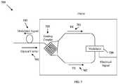
- FIG. 7 is a schematic diagram of an embodiment of a grating coupler based PIRM 700.
- PIRM 700 is a specific embodiment of PIRM 100 and may be used as a PIRM in any system disclosed herein, for example as PIRM 221, PIRM 321, PIRM 413, and/or PIRM 421.
- PIRM 700 receives an optical carrier 741 from off chip.
- PIRM 700 comprises a two-dimension grating coupler 755 (2D-GC) with a specified incidence angle for the waveguide.
- the 2D-GC 755 has two gratings with corresponding orientations orthogonal to each other.
- the optical carrier 741 is split across the grating coupler 755 such that a first optical component is transmitted into the lower waveguide to become the TE component 762 while a second optical component with an orthogonal orientation is transmitted into the upper waveguide to become another TE component 761.
- the grating coupler 755 performed substantially the same function as a PBS 155 and PR 157.
- PIRM 700 comprises a modulator 759, which is substantially similar to modulator 159, and is configured to substantially simultaneously modulate TE components 761-762.
- Modulated TE component 761 returns to the grating coupler 755 in a clockwise direction while modulated TE component 762 returns to the grating coupler 755 in a counter-clockwise direction.
- FIG. 8 is a schematic diagram of an embodiment of a baseband unit (BBU) 800 for use in a CRAN, such as CRAN 200, employing PIRMs, such as PIRMs 100, 221, 500, 600, and/or 700.
- BBU 800 may implement one or more BBU transceivers 211.
- BBU 800 comprises a CW laser 813, and uplink Rx 815, and an OC 818, which are substantially similar to the CW laser 313, the uplink Rx 315, the OC 318, but are not configured for WDM.
- the CW laser 813 generates a single uplink carrier 841 for downstream transmission to the RRU (e.g. RRU 220) via the OC 818, and a modulated uplink signal 843 is received back from the RRU via the same fiber.
- the OC 818 forwards the uplink signal 843 from the RRU into the uplink Rx 815 for conversion into electrical data.
- the BBU 800 further comprises a downlink Tx 817, which is a CW laser with a modulator, such as a modulator 159.
- the downlink Tx 817 creates and modulates an optical carrier, resulting in a downlink signal 845 for transmission to the RRU.
- BBU 800 employs two optical fibers, one for the uplink signal 843 and uplink carrier 841 and one for the downlink signal 845. Further, both lasers (e.g. laser 813 and downlink Tx 817) are positioned in the BBU 800 allowing the RRU to be produced without an on device laser/optical source, while still employing optical communication.
- FIG. 9 is a schematic diagram of another embodiment of a BBU 900 for use in a CRAN, such as CRAN 200, employing PIRMs such as PIRMs 100, 221, 500, 600, and/or 700.
- BBU 900 may implement one or more BBU transceivers 211.
- BBU 900 may be substantially similar to BBU 800 but may employ a single CW laser 913 for both upstream and downstream communications.
- BBU 900 comprises CW laser 913, uplink Rx 915, and OCs 918-919, which are substantially similar to CW laser 813, uplink Rx 815, and OC 818, respectively, but coupled in a different configuration.
- BBU 900 further comprises downlink modulator 917, which is substantially similar to downlink Tx 817, but does not comprise a laser/optical source.
- CW laser 913 transmits an optical carrier, which is split by OC 919 and forwarded to OC 918 as an uplink carrier 941 and forwarded to downlink modulator 917 as a downlink carrier.
- Downlink modulator 917 modulates the downlink carrier to create a downlink signal 945 for transmission to an RRU via a fiber.
- Uplink carrier 941 is forwarded downstream to an RRU, which modulates the uplink carrier 941 into an uplink signal 943 as discussed above.
- the uplink signal 943 is received by OC 918 and forwarded to uplink Rx 915 for conversion into electrical data.
- One or more optical amplifiers may be placed along the light paths as needed to boost the optical signal, for example between OC 918 and uplink Rx 915 and/or between OC 918 and the transmission fiber.
- BBU 900 employs two optical fibers, one for the uplink signal 943 and uplink carrier 941 and one for the downlink signal 945, but employs a single laser 913 per RRU. Further, the laser 913 is positioned in the BBU 900 allowing the RRU to be produced without an on-device laser/optical source, while still employing optical communication.
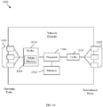
- FIG. 10 is a schematic diagram of an embodiment of an NE 1000 configured to operate in a network, such as networks 200, 300, and/or 400, employing PIRMs, such as PIRMs 100, 500, 600, and/or 700.
- the NE 1000 may be located in an optical transmission system, such as a CRAN or a datacenter network, and may comprise a Tx comprising a PIRM module 1034 (comprising a PIRM but not comprising a corresponding laser).
- the NE 1000 may be configured to implement or support any of the schemes described herein.
- NE 1000 may act as an RRU, BBU, EOR switch, TOR switch, rack server, or any other optical network element disclosed herein.
- transceiver unit encompasses a broad range of devices of which NE 1000 is merely an example.
- NE 1000 is included for purposes of clarity of discussion, but is in no way meant to limit the application of the present disclosure to a particular transceiver unit embodiment or class of transceiver unit embodiments.
- At least some of the features/methods described in the disclosure may be implemented in a network apparatus or component such as a NE 1000.
- the features/methods in the disclosure may be implemented using hardware, firmware, and/or software installed to run on hardware.
- the NE 1000 may be any device that transports electrical, wireless, and/or optical signals through a network, e.g., a switch, router, bridge, server, a client, etc.
- the NE 1000 may comprise transceivers (Tx/Rx) 1010, which may be transmitters, receivers, or combinations thereof, comprising a PIRM.
- Tx/Rx 1010 may be coupled to a plurality of upstream ports 1050 for transmitting and/or receiving optical frames from other nodes and a Tx/Rx 1010 coupled to a plurality of downstream ports 1020 for transmitting and/or receiving frames from other nodes, respectively.
- the Tx/Rx 1010 is an antenna for use in downstream transmissions and downstream ports 1020 are omitted.
- a processor 1030 may be coupled to the Tx/Rxs 1010 to process the data signals and/or determine which nodes to send data signals to.
- the processor 1030 may comprise one or more multi-core processors and/or memory devices 1032, which may function as data stores, buffers, etc.
- Processor 1030 may be implemented as a general processor or may be part of one or more application specific integrated circuits (ASICs) and/or digital signal processors (DSPs).
- the NE 1000 may comprise a PIRM module 1034, which may be configured to modulate a received optical carrier to generate an optical signal for re-transmission as discussed herein.
- the downstream ports 1020 and/or upstream ports 1050 may contain electrical, wireless, and/or optical transmitting and/or receiving components.
- the NE 1000 includes a reception module receiving an optical carrier from a remote device via an optical input port, a splitter module splitting the optical carrier into a first polarized component and a second polarized component such that a first polarization of the first polarized component is perpendicular to a second polarization of the second polarized component, a modulation module modulating an electrical signal onto the first polarized component and the second polarized component, and a combiner module combining the modulated first polarized component and the modulated second polarized component to create a combined modulated signal.
- the NE 1000 may include other or additional modules for performing any one of or combination of steps described in the embodiments.
- FIG. 11 is a flowchart of an embodiment of a method 1100 of PIRM based modulation, for example in a network such as networks 200, 300, and/or 400, employing PIRMs, such as PIRMs 100, 500, 600, and/or 700.
- Method 1100 is initiated when an optical carrier is received from a remote device.
- an optical carrier is received from a remote device via an optical input port.
- the optical carrier is split (by a polarization beam splitter/combiner) into a first polarized portion and a second polarized portion such that a first polarization of the first polarized portion is perpendicular (e.g. orthogonal) to a second polarization of the second polarized portion.
- the two polarizations of the optical carrier are separated and can be managed separately.
- the second polarization of the second polarized portion is rotated (e.g. by a polarization rotator) to be parallel to the first polarization of the first polarized portion prior to modulation.
- an electrical signal is substantially simultaneously modulated onto the first polarized portion and the second polarized portion by employing a single modulator. As discussed above, the first polarized portion and the second polarized portion traverse the modulator in opposite directions (e.g. clockwise and counter-clockwise).
- the modulated first polarized portion and the modulated second polarized portion are returned to the polarization beam splitter/combiner and combined to create a combined modulated signal.
- the combined modulated signal is transmitted via the optical input port over a common optical fiber with the optical carrier.
- FIG. 12 is a graph 1200 of power penalty versus modulator location deviation tolerance for an embodiment of a PIRM, such as PIRMs 100, 221, 321, 413, 421, 500, 600, 700, and 1034.
- BER bit error rate
- BER in graph 1200 is determined based on a Non-return-to-zero (NRZ) with a baud rate of 28 Gigabauds (Gbauds) per second (GBauds/s) and a transmitter and receiver bandwidth of about 0.75 times the baud rate.
- NZ Non-return-to-zero
- Gbauds Gigabauds
- Gauds/s Gigabauds
- the penalty is very small for all the ⁇ evaluated.
- the power penalty to achieve the BER is negligible regardless of ⁇ . Accordingly, so long as a PIRM is at a location within 1-2 ps of the light path center, the power penalty to achieve the desired BER is acceptable.
Landscapes
- Physics & Mathematics (AREA)
- Engineering & Computer Science (AREA)
- Computer Networks & Wireless Communication (AREA)
- Signal Processing (AREA)
- Electromagnetism (AREA)
- Nonlinear Science (AREA)
- Optics & Photonics (AREA)
- General Physics & Mathematics (AREA)
- Computing Systems (AREA)
- Optical Modulation, Optical Deflection, Nonlinear Optics, Optical Demodulation, Optical Logic Elements (AREA)
- Optical Communication System (AREA)
Claims (3)
- Appareil comprenant :une entrée optique (147) configurée pour recevoir une porteuse optique (641) ;un diviseur de faisceau de polarisation (655) couplé optiquement à l'entrée optique (147), un premier trajet lumineux (156) et un second trajet lumineux (158), dans lequel le diviseur de faisceau de polarisation (655) est configuré pour :transmettre un premier composant polarisé de la porteuse optique (641) le long du premier trajet lumineux (156) ; ettransmettre un second composant polarisé de la porteuse optique (641) le long du second trajet lumineux (158), dans lequel le premier composant polarisé comprend une première polarisation qui est perpendiculaire à une seconde polarisation du second composant polarisé lors de la sortie du diviseur de faisceau de polarisation (655) ; etun modulateur optique (659) ayant une extrémité proximale couplée au premier trajet lumineux (156) et une extrémité distale couplée au second trajet lumineux (158), dans lequel le modulateur optique (659) est configuré pour moduler simultanément le premier composant polarisé de la porteuse optique (641) et le second composant polarisé de la porteuse optique (641) par un signal électrique commun, comprenant :la réception du premier composant polarisé à partir du premier trajet lumineux (156) par le biais de l'extrémité proximale ;la réception du second composant polarisé à partir du second trajet lumineux (158) par le biais de l'extrémité distale ;la modulation du premier composant polarisé pour générer un premier composant modulé ;la modulation du second composant polarisé pour générer un second composant modulé ;la sortie du premier composant modulé vers le second trajet lumineux (158) par le biais de l'extrémité distale ; etla sortie du second composant modulé vers le premier trajet lumineux (156) par le biais de l'extrémité proximale ;dans lequel le diviseur de faisceau de polarisation (655) est configuré en outre pour :combiner le premier composant modulé et le second composant modulé dans un signal modulé combiné (643) ; ettransmettre le signal modulé combiné par le biais de l'entrée optique dans une direction opposée à une direction de la porteuse optique (141) ;caractérisé en ce quele premier trajet lumineux (156) et le second trajet lumineux (158) comprennent un guide d'ondes en silicium ;le diviseur de faisceau de polarisation (655) comprend un cristal à biréfringence (651) d'orthovanadate d'yttrium, YV04, un coin de verre (652), une lame demi-onde (653), « HWP » et des coupleurs de réseau de diffraction (657, 656), « GC » ;le cristal à biréfringence (651) est configuré pour diviser la porteuse optique (641) en un rayon ordinaire (663), O-rayon, qui présente une polarisation perpendiculaire à une page, et en un rayon extraordinaire (664), E-rayon, qui présente une polarisation qui est perpendiculaire/orthogonale à l'O-rayon (663) ;le coin de verre (652) est configuré pour courber l'O-rayon (663) et l'E-rayon (664) vers les GC (657, 656) ; etla HWP (653) est positionnée entre le coin de verre (652) et les GC (657, 656), fixée et liée à la surface d'une puce en silicium contenant les GC (657, 656) et configurée pour faire tourner les polarisations de l'O-rayon (663) et de l'E-rayon (664), comme réfléchi par le coin de verre (652), de 45 degrés et pour les aligner avec l'orientation des GC (657, 656) correspondants, entraînant que les polarisations desdits deux rayons sont alignées respectivement avec les modes TE des guides d'ondes en silicium (661, 662) des premier et second trajets lumineux ; etles GC (657, 656) sont des réseaux de résine photosensible configurés pour coupler la lumière dans le guide d'ondes en silicium.
- Appareil selon la revendication 1, dans lequel le modulateur optique (159) comprend un modulateur basé sur un guide d'ondes en silicium.
- Appareil selon la revendication 2, dans lequel le modulateur basé sur le guide d'ondes en silicium est un modulateur de Mach-Zehnder ou un modulateur en quadrature de phase.
Applications Claiming Priority (3)
| Application Number | Priority Date | Filing Date | Title |
|---|---|---|---|
| US201562162161P | 2015-05-15 | 2015-05-15 | |
| US15/136,396 US20160337041A1 (en) | 2015-05-15 | 2016-04-22 | Polarization Independent Reflective Modulator |
| PCT/CN2016/080513 WO2016184301A1 (fr) | 2015-05-15 | 2016-04-28 | Modulateur de réflexion indépendant de la polarisation |
Publications (3)
| Publication Number | Publication Date |
|---|---|
| EP3289407A1 EP3289407A1 (fr) | 2018-03-07 |
| EP3289407A4 EP3289407A4 (fr) | 2018-05-02 |
| EP3289407B1 true EP3289407B1 (fr) | 2019-06-26 |
Family
ID=57277206
Family Applications (1)
| Application Number | Title | Priority Date | Filing Date |
|---|---|---|---|
| EP16795788.5A Active EP3289407B1 (fr) | 2015-05-15 | 2016-04-28 | Modulateur de réflexion indépendant de la polarisation |
Country Status (5)
| Country | Link |
|---|---|
| US (1) | US20160337041A1 (fr) |
| EP (1) | EP3289407B1 (fr) |
| JP (1) | JP6527600B2 (fr) |
| CN (1) | CN107615139B (fr) |
| WO (1) | WO2016184301A1 (fr) |
Families Citing this family (29)
| Publication number | Priority date | Publication date | Assignee | Title |
|---|---|---|---|---|
| US10009106B2 (en) * | 2012-05-14 | 2018-06-26 | Acacia Communications, Inc. | Silicon photonics multicarrier optical transceiver |
| US9647426B1 (en) | 2013-06-28 | 2017-05-09 | Aurrion, Inc. | Polarization insensitive colorless optical devices |
| US10003133B2 (en) * | 2016-01-22 | 2018-06-19 | Telekom Malaysia Berhad | Reusable carrier based polarization diversity for uplink of full-duplex radio-over-fiber system |
| EP3851889B1 (fr) * | 2016-05-25 | 2024-08-07 | OpenLight Photonics, Inc. | Dispositif et procédé de couplage optique |
| US10551640B2 (en) * | 2016-11-21 | 2020-02-04 | Futurewei Technologies, Inc. | Wavelength division multiplexed polarization independent reflective modulators |
| US10222676B2 (en) | 2017-01-27 | 2019-03-05 | Futurewei Technologies, Inc. | Polarization insensitive integrated optical modulator |
| CN110337838B (zh) * | 2017-02-14 | 2021-06-04 | 莫列斯有限公司 | 突破性的模块系统 |
| US10330959B2 (en) | 2017-05-22 | 2019-06-25 | Futurewei Technologies, Inc. | Polarization insensitive micro ring modulator |
| US10243684B2 (en) | 2017-05-23 | 2019-03-26 | Futurewei Technologies, Inc. | Wavelength-division multiplexed polarization-insensitive transmissive modulator |
| CN110149153B (zh) * | 2018-02-13 | 2020-12-01 | 华为技术有限公司 | 光调制器、调制方法及光调制系统 |
| US10651947B2 (en) | 2018-02-20 | 2020-05-12 | Futurewei Technologies, Inc. | Coherent detection with remotely delivered local oscillators |
| US10448127B1 (en) * | 2018-03-22 | 2019-10-15 | Amazon Technologies, Inc. | Network base signal distribution system |
| US10302867B1 (en) * | 2018-04-05 | 2019-05-28 | Northrop Grumman Systems Corporation | Redirected optical modulator output |
| CN108616310B (zh) * | 2018-04-27 | 2020-07-21 | 中国科学院半导体研究所 | 基于马赫增德尔调制器进行四级脉冲幅度调制的方法 |
| US11405125B2 (en) * | 2018-07-12 | 2022-08-02 | Ayar Labs, Inc. | TORminator system and associated methods |
| CN111371499B (zh) * | 2018-12-26 | 2021-08-31 | 中兴光电子技术有限公司 | 一种调制装置和光发射机 |
| CN112134712B (zh) * | 2019-06-25 | 2021-12-31 | 华为技术有限公司 | 一种信号处理方法以及相关设备 |
| CN114079832B (zh) * | 2020-08-21 | 2023-03-28 | 华为技术有限公司 | 一种光源、光传输方法和光注入锁定系统 |
| EP4145200B1 (fr) * | 2021-09-03 | 2025-05-28 | Galina Dr. Georgieva | Élément optique |
| CN114006141B (zh) * | 2021-11-03 | 2022-11-11 | 中国科学院合肥物质科学研究院 | 一种长脉冲高功率毫米波三端口功率分配光栅 |
| CN114466085A (zh) * | 2021-12-30 | 2022-05-10 | 华为技术有限公司 | 一种数据传输方法、射频单元、基带单元及通信系统 |
| DE102022202285A1 (de) | 2022-03-07 | 2023-09-07 | Volkswagen Aktiengesellschaft | Radarsensorvorrichtung, Radarsystem mit einer Radarsensorvorrichtung, Fahrzeug mit einem Radarsystem sowie Verfahren zum Betreiben einer Radarsensorvorrichtung |
| US11923906B2 (en) * | 2022-07-22 | 2024-03-05 | Cisco Technology, Inc. | Laserless optical transceiver |
| US12191910B2 (en) * | 2022-07-22 | 2025-01-07 | Cisco Technology, Inc. | Laserless optical transceiver |
| DE102022121510B3 (de) * | 2022-08-25 | 2023-11-30 | Tesat-Spacecom Gmbh & Co. Kg | Selbstkompensierender Polarisationsmodulator mit direktionalem Phasenschieber, optische Signalübertragungsstrecke und Satellit |
| US12388534B2 (en) * | 2022-12-07 | 2025-08-12 | Lumentum Operations Llc | Co-packaged optics system with a laser source and a bi-directional laser medium |
| CN117375722B (zh) * | 2023-12-08 | 2024-02-06 | 众瑞速联(武汉)科技有限公司 | 偏振复用光传输系统和传输方法 |
| GB2639539A (en) * | 2024-02-21 | 2025-10-01 | Cambridge Consultants | Optical modulation |
| CN119419587B (zh) * | 2024-11-08 | 2025-06-27 | 西安电子科技大学 | 一种窄线宽单纵模种子激光系统及生成方法 |
Family Cites Families (38)
| Publication number | Priority date | Publication date | Assignee | Title |
|---|---|---|---|---|
| US5495366A (en) * | 1993-05-03 | 1996-02-27 | The United States Of America As Represented By The Secretary Of The Navy | Apparatus and method for eliminating polarization sensitivity in transducers |
| JPH09264939A (ja) * | 1996-03-29 | 1997-10-07 | Hitachi Cable Ltd | 偏波無依存型物理量計測方法 |
| AU2748101A (en) * | 1999-10-27 | 2001-06-06 | California Institute Of Technology | Opto-electronic devices for processing and transmitting rf signals based on brillouin selective sideband amplification |
| EP1256819A4 (fr) * | 1999-10-28 | 2006-08-23 | Sharp Kk | Composant optique et procede de fabrication de film polyimide epais |
| KR100325687B1 (ko) * | 1999-12-21 | 2002-02-25 | 윤덕용 | 주입된 비간섭성 광에 파장 잠김된 페브리-페롯 레이저다이오드를 이용한 파장분할 다중방식 광통신용 광원 |
| JP4060551B2 (ja) * | 2000-09-07 | 2008-03-12 | 三菱電機株式会社 | 光信号送信装置及び光信号送信方法 |
| FI20011414L (fi) * | 2001-06-29 | 2002-12-30 | Nokia Corp | Optinen ohjauselementti |
| JP2003169021A (ja) * | 2001-11-30 | 2003-06-13 | Kddi Corp | 光伝送システム |
| KR100496710B1 (ko) * | 2002-01-21 | 2005-06-28 | 노베라옵틱스코리아 주식회사 | 주입된 비간섭성 광에 파장 잠김된 광원을 이용한 양방향파장분할다중방식 수동형 광 네트워크 |
| GB0208255D0 (en) * | 2002-04-10 | 2002-05-22 | Imec Inter Uni Micro Electr | Photonic crystal based fiber-to-waveguide coupler for polarisation independent photonic integrated circuits |
| US7088497B1 (en) * | 2002-12-17 | 2006-08-08 | Silicon Light Machines Corporation | Optical device with polarization diversity module |
| KR100539928B1 (ko) * | 2003-08-29 | 2005-12-28 | 삼성전자주식회사 | 다파장 광원 및 그를 이용한 파장 분할 다중 시스템 |
| KR100575953B1 (ko) * | 2003-10-27 | 2006-05-02 | 삼성전자주식회사 | 반사형 이득고정 반도체 광증폭기를 포함하는 광신호전송장치 및 이를 이용한 광통신 시스템 |
| US7428358B2 (en) * | 2004-01-15 | 2008-09-23 | University Of Delaware | Optical coupler for coupling an optical fiber into a waveguide |
| JP2007534978A (ja) * | 2004-07-22 | 2007-11-29 | 富士通株式会社 | ループ構成を使った全光偏光回転スイッチ |
| KR100675834B1 (ko) * | 2004-10-28 | 2007-01-29 | 한국전자통신연구원 | 루프백 형 파장분할다중방식의 수동형 광 네트워크 |
| US7402773B2 (en) * | 2005-05-24 | 2008-07-22 | Disco Corporation | Laser beam processing machine |
| FR2893469B1 (fr) * | 2005-11-17 | 2007-12-14 | Alcatel Sa | Dispositifs perfectionnes de transmission de donnees pour des equipements de communication d'un reseau optique passif |
| KR100819034B1 (ko) * | 2006-05-11 | 2008-04-03 | 한국전자통신연구원 | 반사형 반도체 광증폭기 기반 수동형 광가입자망 |
| US8369706B2 (en) * | 2006-07-18 | 2013-02-05 | Novera Optics, Inc. | Open access service model using WDM-PON |
| CN100410733C (zh) * | 2006-07-20 | 2008-08-13 | 上海交通大学 | 应用自由空间耦合技术调制光的方法及调制器 |
| KR100890389B1 (ko) * | 2006-12-05 | 2009-03-26 | 한국전자통신연구원 | 편광 무의존 단방향 양자 암호 수신 및 송수신 장치 |
| EP2000836A1 (fr) * | 2007-06-07 | 2008-12-10 | Interuniversitair Microelektronica Centrum | Procédé et système pour un multiplexeur à réseau avec couplage de guides d'ondes optiques |
| CN101841748B (zh) * | 2009-03-17 | 2013-06-12 | 中国移动通信集团公司 | 信号传输系统以及相关装置 |
| CN102308437B (zh) * | 2009-05-26 | 2013-09-11 | 华为技术有限公司 | 一种天线装置 |
| WO2011141682A1 (fr) * | 2010-05-14 | 2011-11-17 | France Telecom | Dispositif de terminaison de ligne optique permettant la mise en œuvre d'une technique de modulation ofdm |
| JP2012203334A (ja) * | 2011-03-28 | 2012-10-22 | Sumitomo Osaka Cement Co Ltd | 光学素子 |
| EP2665212B1 (fr) * | 2012-05-16 | 2016-11-30 | Alcatel Lucent | Système de transmission de données optiques |
| CN102820945B (zh) * | 2012-08-24 | 2015-09-30 | 武汉邮电科学研究院 | 基于奈奎斯特波分复用的无源光网络系统及实现方法 |
| DE102012019472B4 (de) * | 2012-09-28 | 2023-05-04 | Carl Zeiss Microscopy Gmbh | Optische Filtervorrichtung, insbesondere für Mikroskope, und Mikroskop |
| US8948549B2 (en) * | 2012-11-27 | 2015-02-03 | Teraxion Inc. | Polarization rotator assembly including a subwavelength composite portion |
| US9647426B1 (en) * | 2013-06-28 | 2017-05-09 | Aurrion, Inc. | Polarization insensitive colorless optical devices |
| CN103424894B (zh) * | 2013-08-28 | 2015-10-28 | 中国科学院上海光学精密机械研究所 | 偏振无关电光强度调制器 |
| FR3010196B1 (fr) * | 2013-09-02 | 2015-09-18 | Commissariat Energie Atomique | Dispositif de generation d'une modulation d'un signal optique |
| US9977187B2 (en) * | 2014-05-22 | 2018-05-22 | Sifotonics Technologies Co., Ltd. | Polarization rotator-splitter/combiner based on silicon rib-type waveguides |
| CN104049375B (zh) * | 2014-06-05 | 2016-02-24 | 华中科技大学 | 一种偏振无关空间光调制方法和装置 |
| CN104122674B (zh) * | 2014-08-05 | 2016-04-20 | 华中科技大学 | 透射式偏振无关空间光调制方法、装置及所构成的系统 |
| US9874696B2 (en) * | 2015-02-19 | 2018-01-23 | Elenion Technologies, Inc. | Integrated polarization splitter and rotator including a third region for tuning the polarization dependent loss of output transverse electric signals |
-
2016
- 2016-04-22 US US15/136,396 patent/US20160337041A1/en not_active Abandoned
- 2016-04-28 CN CN201680026147.5A patent/CN107615139B/zh active Active
- 2016-04-28 WO PCT/CN2016/080513 patent/WO2016184301A1/fr not_active Ceased
- 2016-04-28 JP JP2017559501A patent/JP6527600B2/ja active Active
- 2016-04-28 EP EP16795788.5A patent/EP3289407B1/fr active Active
Non-Patent Citations (1)
| Title |
|---|
| None * |
Also Published As
| Publication number | Publication date |
|---|---|
| WO2016184301A1 (fr) | 2016-11-24 |
| CN107615139A (zh) | 2018-01-19 |
| JP2018520375A (ja) | 2018-07-26 |
| US20160337041A1 (en) | 2016-11-17 |
| EP3289407A4 (fr) | 2018-05-02 |
| CN107615139B (zh) | 2020-09-18 |
| JP6527600B2 (ja) | 2019-06-05 |
| EP3289407A1 (fr) | 2018-03-07 |
Similar Documents
| Publication | Publication Date | Title |
|---|---|---|
| EP3289407B1 (fr) | Modulateur de réflexion indépendant de la polarisation | |
| US11929826B2 (en) | Optical modules having an improved optical signal to noise ratio | |
| EP3566096B1 (fr) | Modulateur optique intégré insensible à la polarisation | |
| US10203454B2 (en) | Dense wavelength-division multiplexing (DWDM) network and method | |
| US10330959B2 (en) | Polarization insensitive micro ring modulator | |
| EP3398267B1 (fr) | Modulateurs réflectifs indépendants de la polarisation multiplexés par répartition en longueur d'onde | |
| US10178452B2 (en) | Optical interconnect having optical splitters and modulators integrated on same chip | |
| US10075257B2 (en) | Optical spatial division multiplexing usable at short reach | |
| JP2014236420A (ja) | 光源モジュール、および光送受信装置 | |
| Mazurek et al. | Up to 112 Gbit/s single wavelength channel transmission in the 1310 nm wavelength domain | |
| US11924593B1 (en) | Method and system for co-packaged optics | |
| Binh et al. | Integration of Group IV photonic components and other integrated optics and impacts on 5G optical networking | |
| Whaley et al. | Air Force highly integrated photonics program: Development and demonstration of an optically transparent fiber optic network for avionics applications | |
| KR20070020926A (ko) | 광 서큘레이터를 이용한 수동형 광 코어 공유 방법 및시스템 | |
| Li | Silicon Modulators, Switches and Sub-systems for Optical Interconnect |
Legal Events
| Date | Code | Title | Description |
|---|---|---|---|
| STAA | Information on the status of an ep patent application or granted ep patent |
Free format text: STATUS: THE INTERNATIONAL PUBLICATION HAS BEEN MADE |
|
| PUAI | Public reference made under article 153(3) epc to a published international application that has entered the european phase |
Free format text: ORIGINAL CODE: 0009012 |
|
| STAA | Information on the status of an ep patent application or granted ep patent |
Free format text: STATUS: REQUEST FOR EXAMINATION WAS MADE |
|
| 17P | Request for examination filed |
Effective date: 20171127 |
|
| AK | Designated contracting states |
Kind code of ref document: A1 Designated state(s): AL AT BE BG CH CY CZ DE DK EE ES FI FR GB GR HR HU IE IS IT LI LT LU LV MC MK MT NL NO PL PT RO RS SE SI SK SM TR |
|
| AX | Request for extension of the european patent |
Extension state: BA ME |
|
| A4 | Supplementary search report drawn up and despatched |
Effective date: 20180406 |
|
| RIC1 | Information provided on ipc code assigned before grant |
Ipc: H04B 10/50 20130101AFI20180329BHEP Ipc: H04B 10/272 20130101ALI20180329BHEP Ipc: G02F 1/01 20060101ALI20180329BHEP Ipc: H04B 10/2575 20130101ALI20180329BHEP |
|
| DAV | Request for validation of the european patent (deleted) | ||
| DAX | Request for extension of the european patent (deleted) | ||
| REG | Reference to a national code |
Ref country code: DE Ref legal event code: R079 Ref document number: 602016016047 Country of ref document: DE Free format text: PREVIOUS MAIN CLASS: G02F0001010000 Ipc: H04B0010500000 |
|
| RIC1 | Information provided on ipc code assigned before grant |
Ipc: H04B 10/272 20130101ALI20181116BHEP Ipc: G02F 1/01 20060101ALI20181116BHEP Ipc: H04B 10/50 20130101AFI20181116BHEP Ipc: H04B 10/2575 20130101ALI20181116BHEP |
|
| GRAP | Despatch of communication of intention to grant a patent |
Free format text: ORIGINAL CODE: EPIDOSNIGR1 |
|
| STAA | Information on the status of an ep patent application or granted ep patent |
Free format text: STATUS: GRANT OF PATENT IS INTENDED |
|
| RIN1 | Information on inventor provided before grant (corrected) |
Inventor name: ZHU, FEI Inventor name: BAI, YUSHENG Inventor name: WEN, YANGJING |
|
| INTG | Intention to grant announced |
Effective date: 20190111 |
|
| GRAS | Grant fee paid |
Free format text: ORIGINAL CODE: EPIDOSNIGR3 |
|
| GRAA | (expected) grant |
Free format text: ORIGINAL CODE: 0009210 |
|
| STAA | Information on the status of an ep patent application or granted ep patent |
Free format text: STATUS: THE PATENT HAS BEEN GRANTED |
|
| AK | Designated contracting states |
Kind code of ref document: B1 Designated state(s): AL AT BE BG CH CY CZ DE DK EE ES FI FR GB GR HR HU IE IS IT LI LT LU LV MC MK MT NL NO PL PT RO RS SE SI SK SM TR |
|
| REG | Reference to a national code |
Ref country code: GB Ref legal event code: FG4D |
|
| REG | Reference to a national code |
Ref country code: CH Ref legal event code: EP |
|
| REG | Reference to a national code |
Ref country code: AT Ref legal event code: REF Ref document number: 1149528 Country of ref document: AT Kind code of ref document: T Effective date: 20190715 |
|
| REG | Reference to a national code |
Ref country code: IE Ref legal event code: FG4D |
|
| REG | Reference to a national code |
Ref country code: DE Ref legal event code: R096 Ref document number: 602016016047 Country of ref document: DE |
|
| REG | Reference to a national code |
Ref country code: NL Ref legal event code: MP Effective date: 20190626 |
|
| PG25 | Lapsed in a contracting state [announced via postgrant information from national office to epo] |
Ref country code: LT Free format text: LAPSE BECAUSE OF FAILURE TO SUBMIT A TRANSLATION OF THE DESCRIPTION OR TO PAY THE FEE WITHIN THE PRESCRIBED TIME-LIMIT Effective date: 20190626 Ref country code: FI Free format text: LAPSE BECAUSE OF FAILURE TO SUBMIT A TRANSLATION OF THE DESCRIPTION OR TO PAY THE FEE WITHIN THE PRESCRIBED TIME-LIMIT Effective date: 20190626 Ref country code: HR Free format text: LAPSE BECAUSE OF FAILURE TO SUBMIT A TRANSLATION OF THE DESCRIPTION OR TO PAY THE FEE WITHIN THE PRESCRIBED TIME-LIMIT Effective date: 20190626 Ref country code: NO Free format text: LAPSE BECAUSE OF FAILURE TO SUBMIT A TRANSLATION OF THE DESCRIPTION OR TO PAY THE FEE WITHIN THE PRESCRIBED TIME-LIMIT Effective date: 20190926 Ref country code: AL Free format text: LAPSE BECAUSE OF FAILURE TO SUBMIT A TRANSLATION OF THE DESCRIPTION OR TO PAY THE FEE WITHIN THE PRESCRIBED TIME-LIMIT Effective date: 20190626 Ref country code: SE Free format text: LAPSE BECAUSE OF FAILURE TO SUBMIT A TRANSLATION OF THE DESCRIPTION OR TO PAY THE FEE WITHIN THE PRESCRIBED TIME-LIMIT Effective date: 20190626 |
|
| REG | Reference to a national code |
Ref country code: LT Ref legal event code: MG4D |
|
| PG25 | Lapsed in a contracting state [announced via postgrant information from national office to epo] |
Ref country code: GR Free format text: LAPSE BECAUSE OF FAILURE TO SUBMIT A TRANSLATION OF THE DESCRIPTION OR TO PAY THE FEE WITHIN THE PRESCRIBED TIME-LIMIT Effective date: 20190927 Ref country code: LV Free format text: LAPSE BECAUSE OF FAILURE TO SUBMIT A TRANSLATION OF THE DESCRIPTION OR TO PAY THE FEE WITHIN THE PRESCRIBED TIME-LIMIT Effective date: 20190626 Ref country code: RS Free format text: LAPSE BECAUSE OF FAILURE TO SUBMIT A TRANSLATION OF THE DESCRIPTION OR TO PAY THE FEE WITHIN THE PRESCRIBED TIME-LIMIT Effective date: 20190626 Ref country code: BG Free format text: LAPSE BECAUSE OF FAILURE TO SUBMIT A TRANSLATION OF THE DESCRIPTION OR TO PAY THE FEE WITHIN THE PRESCRIBED TIME-LIMIT Effective date: 20190926 |
|
| REG | Reference to a national code |
Ref country code: AT Ref legal event code: MK05 Ref document number: 1149528 Country of ref document: AT Kind code of ref document: T Effective date: 20190626 |
|
| PG25 | Lapsed in a contracting state [announced via postgrant information from national office to epo] |
Ref country code: EE Free format text: LAPSE BECAUSE OF FAILURE TO SUBMIT A TRANSLATION OF THE DESCRIPTION OR TO PAY THE FEE WITHIN THE PRESCRIBED TIME-LIMIT Effective date: 20190626 Ref country code: SK Free format text: LAPSE BECAUSE OF FAILURE TO SUBMIT A TRANSLATION OF THE DESCRIPTION OR TO PAY THE FEE WITHIN THE PRESCRIBED TIME-LIMIT Effective date: 20190626 Ref country code: CZ Free format text: LAPSE BECAUSE OF FAILURE TO SUBMIT A TRANSLATION OF THE DESCRIPTION OR TO PAY THE FEE WITHIN THE PRESCRIBED TIME-LIMIT Effective date: 20190626 Ref country code: RO Free format text: LAPSE BECAUSE OF FAILURE TO SUBMIT A TRANSLATION OF THE DESCRIPTION OR TO PAY THE FEE WITHIN THE PRESCRIBED TIME-LIMIT Effective date: 20190626 Ref country code: NL Free format text: LAPSE BECAUSE OF FAILURE TO SUBMIT A TRANSLATION OF THE DESCRIPTION OR TO PAY THE FEE WITHIN THE PRESCRIBED TIME-LIMIT Effective date: 20190626 Ref country code: PT Free format text: LAPSE BECAUSE OF FAILURE TO SUBMIT A TRANSLATION OF THE DESCRIPTION OR TO PAY THE FEE WITHIN THE PRESCRIBED TIME-LIMIT Effective date: 20191028 Ref country code: AT Free format text: LAPSE BECAUSE OF FAILURE TO SUBMIT A TRANSLATION OF THE DESCRIPTION OR TO PAY THE FEE WITHIN THE PRESCRIBED TIME-LIMIT Effective date: 20190626 |
|
| PG25 | Lapsed in a contracting state [announced via postgrant information from national office to epo] |
Ref country code: SM Free format text: LAPSE BECAUSE OF FAILURE TO SUBMIT A TRANSLATION OF THE DESCRIPTION OR TO PAY THE FEE WITHIN THE PRESCRIBED TIME-LIMIT Effective date: 20190626 Ref country code: IS Free format text: LAPSE BECAUSE OF FAILURE TO SUBMIT A TRANSLATION OF THE DESCRIPTION OR TO PAY THE FEE WITHIN THE PRESCRIBED TIME-LIMIT Effective date: 20191026 Ref country code: IT Free format text: LAPSE BECAUSE OF FAILURE TO SUBMIT A TRANSLATION OF THE DESCRIPTION OR TO PAY THE FEE WITHIN THE PRESCRIBED TIME-LIMIT Effective date: 20190626 Ref country code: ES Free format text: LAPSE BECAUSE OF FAILURE TO SUBMIT A TRANSLATION OF THE DESCRIPTION OR TO PAY THE FEE WITHIN THE PRESCRIBED TIME-LIMIT Effective date: 20190626 |
|
| PG25 | Lapsed in a contracting state [announced via postgrant information from national office to epo] |
Ref country code: TR Free format text: LAPSE BECAUSE OF FAILURE TO SUBMIT A TRANSLATION OF THE DESCRIPTION OR TO PAY THE FEE WITHIN THE PRESCRIBED TIME-LIMIT Effective date: 20190626 |
|
| PG25 | Lapsed in a contracting state [announced via postgrant information from national office to epo] |
Ref country code: PL Free format text: LAPSE BECAUSE OF FAILURE TO SUBMIT A TRANSLATION OF THE DESCRIPTION OR TO PAY THE FEE WITHIN THE PRESCRIBED TIME-LIMIT Effective date: 20190626 Ref country code: DK Free format text: LAPSE BECAUSE OF FAILURE TO SUBMIT A TRANSLATION OF THE DESCRIPTION OR TO PAY THE FEE WITHIN THE PRESCRIBED TIME-LIMIT Effective date: 20190626 |
|
| PG25 | Lapsed in a contracting state [announced via postgrant information from national office to epo] |
Ref country code: IS Free format text: LAPSE BECAUSE OF FAILURE TO SUBMIT A TRANSLATION OF THE DESCRIPTION OR TO PAY THE FEE WITHIN THE PRESCRIBED TIME-LIMIT Effective date: 20200320 |
|
| REG | Reference to a national code |
Ref country code: DE Ref legal event code: R097 Ref document number: 602016016047 Country of ref document: DE |
|
| PLBE | No opposition filed within time limit |
Free format text: ORIGINAL CODE: 0009261 |
|
| STAA | Information on the status of an ep patent application or granted ep patent |
Free format text: STATUS: NO OPPOSITION FILED WITHIN TIME LIMIT |
|
| PG2D | Information on lapse in contracting state deleted |
Ref country code: IS |
|
| 26N | No opposition filed |
Effective date: 20200603 |
|
| PG25 | Lapsed in a contracting state [announced via postgrant information from national office to epo] |
Ref country code: SI Free format text: LAPSE BECAUSE OF FAILURE TO SUBMIT A TRANSLATION OF THE DESCRIPTION OR TO PAY THE FEE WITHIN THE PRESCRIBED TIME-LIMIT Effective date: 20190626 |
|
| PG25 | Lapsed in a contracting state [announced via postgrant information from national office to epo] |
Ref country code: MC Free format text: LAPSE BECAUSE OF FAILURE TO SUBMIT A TRANSLATION OF THE DESCRIPTION OR TO PAY THE FEE WITHIN THE PRESCRIBED TIME-LIMIT Effective date: 20190626 |
|
| REG | Reference to a national code |
Ref country code: CH Ref legal event code: PL |
|
| PG25 | Lapsed in a contracting state [announced via postgrant information from national office to epo] |
Ref country code: FR Free format text: LAPSE BECAUSE OF NON-PAYMENT OF DUE FEES Effective date: 20200430 Ref country code: LU Free format text: LAPSE BECAUSE OF NON-PAYMENT OF DUE FEES Effective date: 20200428 Ref country code: CH Free format text: LAPSE BECAUSE OF NON-PAYMENT OF DUE FEES Effective date: 20200430 Ref country code: LI Free format text: LAPSE BECAUSE OF NON-PAYMENT OF DUE FEES Effective date: 20200430 |
|
| REG | Reference to a national code |
Ref country code: BE Ref legal event code: MM Effective date: 20200430 |
|
| PG25 | Lapsed in a contracting state [announced via postgrant information from national office to epo] |
Ref country code: BE Free format text: LAPSE BECAUSE OF NON-PAYMENT OF DUE FEES Effective date: 20200430 |
|
| GBPC | Gb: european patent ceased through non-payment of renewal fee |
Effective date: 20200428 |
|
| PG25 | Lapsed in a contracting state [announced via postgrant information from national office to epo] |
Ref country code: IE Free format text: LAPSE BECAUSE OF NON-PAYMENT OF DUE FEES Effective date: 20200428 Ref country code: GB Free format text: LAPSE BECAUSE OF NON-PAYMENT OF DUE FEES Effective date: 20200428 |
|
| PG25 | Lapsed in a contracting state [announced via postgrant information from national office to epo] |
Ref country code: MT Free format text: LAPSE BECAUSE OF FAILURE TO SUBMIT A TRANSLATION OF THE DESCRIPTION OR TO PAY THE FEE WITHIN THE PRESCRIBED TIME-LIMIT Effective date: 20190626 Ref country code: CY Free format text: LAPSE BECAUSE OF FAILURE TO SUBMIT A TRANSLATION OF THE DESCRIPTION OR TO PAY THE FEE WITHIN THE PRESCRIBED TIME-LIMIT Effective date: 20190626 |
|
| PG25 | Lapsed in a contracting state [announced via postgrant information from national office to epo] |
Ref country code: MK Free format text: LAPSE BECAUSE OF FAILURE TO SUBMIT A TRANSLATION OF THE DESCRIPTION OR TO PAY THE FEE WITHIN THE PRESCRIBED TIME-LIMIT Effective date: 20190626 |
|
| P01 | Opt-out of the competence of the unified patent court (upc) registered |
Effective date: 20230524 |
|
| PGFP | Annual fee paid to national office [announced via postgrant information from national office to epo] |
Ref country code: DE Payment date: 20250305 Year of fee payment: 10 |