EP3294727B1 - Diode électroluminescente organique comprenant différents composés matriciels dans la première et la seconde couche de transport d'électrons - Google Patents
Diode électroluminescente organique comprenant différents composés matriciels dans la première et la seconde couche de transport d'électrons Download PDFInfo
- Publication number
- EP3294727B1 EP3294727B1 EP16722873.3A EP16722873A EP3294727B1 EP 3294727 B1 EP3294727 B1 EP 3294727B1 EP 16722873 A EP16722873 A EP 16722873A EP 3294727 B1 EP3294727 B1 EP 3294727B1
- Authority
- EP
- European Patent Office
- Prior art keywords
- phenyl
- electron transport
- transport layer
- group
- diyl
- Prior art date
- Legal status (The legal status is an assumption and is not a legal conclusion. Google has not performed a legal analysis and makes no representation as to the accuracy of the status listed.)
- Active
Links
- 0 **[n]1c(-c2ncccc2)nc2ccccc12 Chemical compound **[n]1c(-c2ncccc2)nc2ccccc12 0.000 description 23
- RGPPFRDIALTNDG-UHFFFAOYSA-N c(cc1)cc2c1nc(-c1ncccc1)[n]2-c(cc1)ccc1-c1cc(-c2c(ccc3ccccc33)c3nc3c2ccc2c3cccc2)ccc1 Chemical compound c(cc1)cc2c1nc(-c1ncccc1)[n]2-c(cc1)ccc1-c1cc(-c2c(ccc3ccccc33)c3nc3c2ccc2c3cccc2)ccc1 RGPPFRDIALTNDG-UHFFFAOYSA-N 0.000 description 2
- OQURDXRFWFPZGC-UHFFFAOYSA-N C(C1)c2ccccc2-c2c1c(-c1cccc(-c(cc3)ccc3-[n]3c(-c4ccccn4)nc4c3cccc4)c1)c(CCc1ccccc1-1)c-1n2 Chemical compound C(C1)c2ccccc2-c2c1c(-c1cccc(-c(cc3)ccc3-[n]3c(-c4ccccn4)nc4c3cccc4)c1)c(CCc1ccccc1-1)c-1n2 OQURDXRFWFPZGC-UHFFFAOYSA-N 0.000 description 1
- AHCKQUCVVVLQIV-UHFFFAOYSA-N Cc(cc1)ccc1-c(cc(-c1ccccc1)c1ccc2c(-c3ccccc3)c3)nc1c2nc3-c1ccc(C)cc1 Chemical compound Cc(cc1)ccc1-c(cc(-c1ccccc1)c1ccc2c(-c3ccccc3)c3)nc1c2nc3-c1ccc(C)cc1 AHCKQUCVVVLQIV-UHFFFAOYSA-N 0.000 description 1
- BRRCLVISKBDFDE-UHFFFAOYSA-N c(cc1)cc2c1nc(-c1ccccn1)[n]2-c1cc(-c2ccc(cc3)c4c2ccc2c4c3ccc2)cc(-c2ccc(cc3)c4c2ccc2cccc3c42)c1 Chemical compound c(cc1)cc2c1nc(-c1ccccn1)[n]2-c1cc(-c2ccc(cc3)c4c2ccc2c4c3ccc2)cc(-c2ccc(cc3)c4c2ccc2cccc3c42)c1 BRRCLVISKBDFDE-UHFFFAOYSA-N 0.000 description 1
- UROKOGCYURKCJF-UHFFFAOYSA-N c(cc1)cc2c1nc(-c1ncccc1)[n]2-c1cc(-c(cc2)ccc2-c2c(ccc3ccccc33)c3nc3c2ccc2ccccc32)ccc1 Chemical compound c(cc1)cc2c1nc(-c1ncccc1)[n]2-c1cc(-c(cc2)ccc2-c2c(ccc3ccccc33)c3nc3c2ccc2ccccc32)ccc1 UROKOGCYURKCJF-UHFFFAOYSA-N 0.000 description 1
- CQMBTGPLESTEKG-UHFFFAOYSA-N c(cc12)ccc1nc(-c1ccccn1)[n]2-c(cc1)ccc1-c1ccc(cc2)c3c1ccc1c3c2ccc1 Chemical compound c(cc12)ccc1nc(-c1ccccn1)[n]2-c(cc1)ccc1-c1ccc(cc2)c3c1ccc1c3c2ccc1 CQMBTGPLESTEKG-UHFFFAOYSA-N 0.000 description 1
- IEXQHGWXOQPMQO-UHFFFAOYSA-N c1ccc(cc(cc2)-c3nc(-c(cc4)ccc4-c4ncc(cccc5)c5c4)nc(-c4cc(cccc5)c5cc4)n3)c2c1 Chemical compound c1ccc(cc(cc2)-c3nc(-c(cc4)ccc4-c4ncc(cccc5)c5c4)nc(-c4cc(cccc5)c5cc4)n3)c2c1 IEXQHGWXOQPMQO-UHFFFAOYSA-N 0.000 description 1
Images


Classifications
-
- H—ELECTRICITY
- H10—SEMICONDUCTOR DEVICES; ELECTRIC SOLID-STATE DEVICES NOT OTHERWISE PROVIDED FOR
- H10K—ORGANIC ELECTRIC SOLID-STATE DEVICES
- H10K85/00—Organic materials used in the body or electrodes of devices covered by this subclass
- H10K85/60—Organic compounds having low molecular weight
- H10K85/649—Aromatic compounds comprising a hetero atom
- H10K85/654—Aromatic compounds comprising a hetero atom comprising only nitrogen as heteroatom
-
- C—CHEMISTRY; METALLURGY
- C07—ORGANIC CHEMISTRY
- C07D—HETEROCYCLIC COMPOUNDS
- C07D401/00—Heterocyclic compounds containing two or more hetero rings, having nitrogen atoms as the only ring hetero atoms, at least one ring being a six-membered ring with only one nitrogen atom
- C07D401/14—Heterocyclic compounds containing two or more hetero rings, having nitrogen atoms as the only ring hetero atoms, at least one ring being a six-membered ring with only one nitrogen atom containing three or more hetero rings
-
- C—CHEMISTRY; METALLURGY
- C07—ORGANIC CHEMISTRY
- C07D—HETEROCYCLIC COMPOUNDS
- C07D401/00—Heterocyclic compounds containing two or more hetero rings, having nitrogen atoms as the only ring hetero atoms, at least one ring being a six-membered ring with only one nitrogen atom
- C07D401/02—Heterocyclic compounds containing two or more hetero rings, having nitrogen atoms as the only ring hetero atoms, at least one ring being a six-membered ring with only one nitrogen atom containing two hetero rings
- C07D401/04—Heterocyclic compounds containing two or more hetero rings, having nitrogen atoms as the only ring hetero atoms, at least one ring being a six-membered ring with only one nitrogen atom containing two hetero rings directly linked by a ring-member-to-ring-member bond
-
- C—CHEMISTRY; METALLURGY
- C07—ORGANIC CHEMISTRY
- C07D—HETEROCYCLIC COMPOUNDS
- C07D405/00—Heterocyclic compounds containing both one or more hetero rings having oxygen atoms as the only ring hetero atoms, and one or more rings having nitrogen as the only ring hetero atom
- C07D405/14—Heterocyclic compounds containing both one or more hetero rings having oxygen atoms as the only ring hetero atoms, and one or more rings having nitrogen as the only ring hetero atom containing three or more hetero rings
-
- C—CHEMISTRY; METALLURGY
- C09—DYES; PAINTS; POLISHES; NATURAL RESINS; ADHESIVES; COMPOSITIONS NOT OTHERWISE PROVIDED FOR; APPLICATIONS OF MATERIALS NOT OTHERWISE PROVIDED FOR
- C09K—MATERIALS FOR MISCELLANEOUS APPLICATIONS, NOT PROVIDED FOR ELSEWHERE
- C09K11/00—Luminescent materials, e.g. electroluminescent or chemiluminescent
- C09K11/06—Luminescent materials, e.g. electroluminescent or chemiluminescent containing organic luminescent materials
-
- H—ELECTRICITY
- H10—SEMICONDUCTOR DEVICES; ELECTRIC SOLID-STATE DEVICES NOT OTHERWISE PROVIDED FOR
- H10K—ORGANIC ELECTRIC SOLID-STATE DEVICES
- H10K50/00—Organic light-emitting devices
- H10K50/10—OLEDs or polymer light-emitting diodes [PLED]
- H10K50/14—Carrier transporting layers
- H10K50/16—Electron transporting layers
- H10K50/165—Electron transporting layers comprising dopants
-
- H—ELECTRICITY
- H10—SEMICONDUCTOR DEVICES; ELECTRIC SOLID-STATE DEVICES NOT OTHERWISE PROVIDED FOR
- H10K—ORGANIC ELECTRIC SOLID-STATE DEVICES
- H10K50/00—Organic light-emitting devices
- H10K50/10—OLEDs or polymer light-emitting diodes [PLED]
- H10K50/14—Carrier transporting layers
- H10K50/16—Electron transporting layers
- H10K50/166—Electron transporting layers comprising a multilayered structure
-
- H—ELECTRICITY
- H10—SEMICONDUCTOR DEVICES; ELECTRIC SOLID-STATE DEVICES NOT OTHERWISE PROVIDED FOR
- H10K—ORGANIC ELECTRIC SOLID-STATE DEVICES
- H10K50/00—Organic light-emitting devices
- H10K50/10—OLEDs or polymer light-emitting diodes [PLED]
- H10K50/17—Carrier injection layers
- H10K50/171—Electron injection layers
-
- H—ELECTRICITY
- H10—SEMICONDUCTOR DEVICES; ELECTRIC SOLID-STATE DEVICES NOT OTHERWISE PROVIDED FOR
- H10K—ORGANIC ELECTRIC SOLID-STATE DEVICES
- H10K71/00—Manufacture or treatment specially adapted for the organic devices covered by this subclass
- H10K71/40—Thermal treatment, e.g. annealing in the presence of a solvent vapour
- H10K71/441—Thermal treatment, e.g. annealing in the presence of a solvent vapour in the presence of solvent vapors, e.g. solvent vapour annealing
-
- H—ELECTRICITY
- H10—SEMICONDUCTOR DEVICES; ELECTRIC SOLID-STATE DEVICES NOT OTHERWISE PROVIDED FOR
- H10K—ORGANIC ELECTRIC SOLID-STATE DEVICES
- H10K85/00—Organic materials used in the body or electrodes of devices covered by this subclass
- H10K85/30—Coordination compounds
-
- H—ELECTRICITY
- H10—SEMICONDUCTOR DEVICES; ELECTRIC SOLID-STATE DEVICES NOT OTHERWISE PROVIDED FOR
- H10K—ORGANIC ELECTRIC SOLID-STATE DEVICES
- H10K85/00—Organic materials used in the body or electrodes of devices covered by this subclass
- H10K85/60—Organic compounds having low molecular weight
- H10K85/615—Polycyclic condensed aromatic hydrocarbons, e.g. anthracene
-
- H—ELECTRICITY
- H10—SEMICONDUCTOR DEVICES; ELECTRIC SOLID-STATE DEVICES NOT OTHERWISE PROVIDED FOR
- H10K—ORGANIC ELECTRIC SOLID-STATE DEVICES
- H10K85/00—Organic materials used in the body or electrodes of devices covered by this subclass
- H10K85/60—Organic compounds having low molecular weight
- H10K85/615—Polycyclic condensed aromatic hydrocarbons, e.g. anthracene
- H10K85/622—Polycyclic condensed aromatic hydrocarbons, e.g. anthracene containing four rings, e.g. pyrene
-
- H—ELECTRICITY
- H10—SEMICONDUCTOR DEVICES; ELECTRIC SOLID-STATE DEVICES NOT OTHERWISE PROVIDED FOR
- H10K—ORGANIC ELECTRIC SOLID-STATE DEVICES
- H10K85/00—Organic materials used in the body or electrodes of devices covered by this subclass
- H10K85/60—Organic compounds having low molecular weight
- H10K85/615—Polycyclic condensed aromatic hydrocarbons, e.g. anthracene
- H10K85/626—Polycyclic condensed aromatic hydrocarbons, e.g. anthracene containing more than one polycyclic condensed aromatic rings, e.g. bis-anthracene
-
- H—ELECTRICITY
- H10—SEMICONDUCTOR DEVICES; ELECTRIC SOLID-STATE DEVICES NOT OTHERWISE PROVIDED FOR
- H10K—ORGANIC ELECTRIC SOLID-STATE DEVICES
- H10K85/00—Organic materials used in the body or electrodes of devices covered by this subclass
- H10K85/60—Organic compounds having low molecular weight
- H10K85/649—Aromatic compounds comprising a hetero atom
- H10K85/657—Polycyclic condensed heteroaromatic hydrocarbons
- H10K85/6572—Polycyclic condensed heteroaromatic hydrocarbons comprising only nitrogen in the heteroaromatic polycondensed ring system, e.g. phenanthroline or carbazole
-
- H—ELECTRICITY
- H10—SEMICONDUCTOR DEVICES; ELECTRIC SOLID-STATE DEVICES NOT OTHERWISE PROVIDED FOR
- H10K—ORGANIC ELECTRIC SOLID-STATE DEVICES
- H10K85/00—Organic materials used in the body or electrodes of devices covered by this subclass
- H10K85/60—Organic compounds having low molecular weight
- H10K85/649—Aromatic compounds comprising a hetero atom
- H10K85/657—Polycyclic condensed heteroaromatic hydrocarbons
- H10K85/6574—Polycyclic condensed heteroaromatic hydrocarbons comprising only oxygen in the heteroaromatic polycondensed ring system, e.g. cumarine dyes
-
- C—CHEMISTRY; METALLURGY
- C09—DYES; PAINTS; POLISHES; NATURAL RESINS; ADHESIVES; COMPOSITIONS NOT OTHERWISE PROVIDED FOR; APPLICATIONS OF MATERIALS NOT OTHERWISE PROVIDED FOR
- C09K—MATERIALS FOR MISCELLANEOUS APPLICATIONS, NOT PROVIDED FOR ELSEWHERE
- C09K2211/00—Chemical nature of organic luminescent or tenebrescent compounds
- C09K2211/10—Non-macromolecular compounds
- C09K2211/1003—Carbocyclic compounds
- C09K2211/1007—Non-condensed systems
-
- C—CHEMISTRY; METALLURGY
- C09—DYES; PAINTS; POLISHES; NATURAL RESINS; ADHESIVES; COMPOSITIONS NOT OTHERWISE PROVIDED FOR; APPLICATIONS OF MATERIALS NOT OTHERWISE PROVIDED FOR
- C09K—MATERIALS FOR MISCELLANEOUS APPLICATIONS, NOT PROVIDED FOR ELSEWHERE
- C09K2211/00—Chemical nature of organic luminescent or tenebrescent compounds
- C09K2211/10—Non-macromolecular compounds
- C09K2211/1018—Heterocyclic compounds
- C09K2211/1025—Heterocyclic compounds characterised by ligands
- C09K2211/1029—Heterocyclic compounds characterised by ligands containing one nitrogen atom as the heteroatom
-
- C—CHEMISTRY; METALLURGY
- C09—DYES; PAINTS; POLISHES; NATURAL RESINS; ADHESIVES; COMPOSITIONS NOT OTHERWISE PROVIDED FOR; APPLICATIONS OF MATERIALS NOT OTHERWISE PROVIDED FOR
- C09K—MATERIALS FOR MISCELLANEOUS APPLICATIONS, NOT PROVIDED FOR ELSEWHERE
- C09K2211/00—Chemical nature of organic luminescent or tenebrescent compounds
- C09K2211/18—Metal complexes
- C09K2211/185—Metal complexes of the platinum group, i.e. Os, Ir, Pt, Ru, Rh or Pd
-
- H—ELECTRICITY
- H10—SEMICONDUCTOR DEVICES; ELECTRIC SOLID-STATE DEVICES NOT OTHERWISE PROVIDED FOR
- H10K—ORGANIC ELECTRIC SOLID-STATE DEVICES
- H10K2102/00—Constructional details relating to the organic devices covered by this subclass
-
- H—ELECTRICITY
- H10—SEMICONDUCTOR DEVICES; ELECTRIC SOLID-STATE DEVICES NOT OTHERWISE PROVIDED FOR
- H10K—ORGANIC ELECTRIC SOLID-STATE DEVICES
- H10K71/00—Manufacture or treatment specially adapted for the organic devices covered by this subclass
-
- H—ELECTRICITY
- H10—SEMICONDUCTOR DEVICES; ELECTRIC SOLID-STATE DEVICES NOT OTHERWISE PROVIDED FOR
- H10K—ORGANIC ELECTRIC SOLID-STATE DEVICES
- H10K71/00—Manufacture or treatment specially adapted for the organic devices covered by this subclass
- H10K71/10—Deposition of organic active material
- H10K71/12—Deposition of organic active material using liquid deposition, e.g. spin coating
-
- H—ELECTRICITY
- H10—SEMICONDUCTOR DEVICES; ELECTRIC SOLID-STATE DEVICES NOT OTHERWISE PROVIDED FOR
- H10K—ORGANIC ELECTRIC SOLID-STATE DEVICES
- H10K71/00—Manufacture or treatment specially adapted for the organic devices covered by this subclass
- H10K71/10—Deposition of organic active material
- H10K71/16—Deposition of organic active material using physical vapour deposition [PVD], e.g. vacuum deposition or sputtering
- H10K71/164—Deposition of organic active material using physical vapour deposition [PVD], e.g. vacuum deposition or sputtering using vacuum deposition
-
- H—ELECTRICITY
- H10—SEMICONDUCTOR DEVICES; ELECTRIC SOLID-STATE DEVICES NOT OTHERWISE PROVIDED FOR
- H10K—ORGANIC ELECTRIC SOLID-STATE DEVICES
- H10K71/00—Manufacture or treatment specially adapted for the organic devices covered by this subclass
- H10K71/30—Doping active layers, e.g. electron transporting layers
Definitions
- the present invention relates to an organic light-emitting diode containing electron transport layers with different matrix compounds in the first and second electron transport layer and a method of manufacturing the same.
- OLEDs Organic light-emitting diodes
- a typical OLED includes an anode, a hole transport layer (HTL), an emission layer (EML), an electron transport layer (ETL), and a cathode, which are sequentially stacked on a substrate.
- HTL hole transport layer
- EML emission layer
- ETL electron transport layer
- cathode cathode
- the HTL, the EML, and the ETL are thin films formed from organic and / or organometallic compounds.
- US 2014/103306 A1 refers to an organic light-emitting diode comprising: a substrate; a first electrode on the substrate; a second electrode opposite to the first electrode; an emission layer between the first electrode and the second electrode; and an electron transport layer between the emission layer and the second electrode, wherein the electron transport layer comprises a stack structure including n number of electron transport units (where n is an integer of 1 or greater) each including a stack of a first layer, a first mixed layer, a second layer, a second mixed layer, and a third layer that are sequentially stacked upon one another, the first mixed layer and the second mixed layer each comprise an electron-transporting organic material and an electron migration-facilitating material, and the first layer comprises a first electron migration-facilitating material and excludes the electron-transporting organic material, the second layer comprises a second electron migration-facilitating material and excludes the electron-transporting organic material, and the third layer comprises a third electron migration-facilitating material and excludes the electron-transporting organic material.
- n is an integer of 1 or greater
- WO 2013/009095 refers to a triphenylene-based compound and an organic light emitting compound and an organic electroluminescent diode comprising same, and more particularly, to a novel organic light emitting compound that is used as a material for injecting and transferring holes or electrons and emitting light, and to an organic electroluminescent diode using the organic light emitting compound.
- KR 2014 0012920 A refers to an anthracene derivative and an organic electronic device using the same.
- the new anthracene derivative can be used as a material for an organic material layer of the organic electronic device including an organic electroluminescent device, and the organic electronic device by the present invention has excellent properties including efficiency increase, driving voltage decrease, lifetime extension, and stability increase.
- EP 2 700 695 A1 refers to compound for an organic optoelectronic device represented by the following Chemical Formula 2:
- KR 2014 0141337 A refers to an organic compound represented by chemical formula below: and an organic photoelectronic device and a display apparatus comprising the organic compound.
- JP 2007 049055 A refers to an organic EL element material has 9,9-diphenyl fluorene structure, and in 4- and/or 4'- level of phenyl group, the nitrogen-containing heterocycle dielectric such as for example pyrrole and carbazole or the like is combined with N atom.
- EP 2 37 2 803 A1 refers to a material for organic electroluminescence device represented by the following formula:
- US 2010/039027 A1 refers to an organic electroluminescent device comprising, a cathode, an anode, and at least an emitting layer and an electron transporting layer between the cathode and the anode, the emitting layer comprising a host compound and a fluoranthene compound, the electron transporting layer comprising a compound represented by formula: (A)u-(B)v; wherein A is a group containing an aromatic hydrocarbon group having 3 or more carbon rings, B is a heterocyclic group which may be substituted, and u and v are each an integer of 1 to 6.
- GUO-GANG SHAN ET AL "Enhancing the luminescence properties and stability of cationic iridium(iii) complexes based on phenylbenzoimidazole ligand: a combined experimental and theoretical study", DALTON TRANSACTIONS, (20130101), vol. 42, no. 31, ISSN 1477-9226, pages 11056 - 11065 .
- NAN WANG ET AL "Ru-Pt and Ru-Pd heterobimetallic complexes based on a new ligand with two distinct chelate sites", DALTON TRANSACTIONS: THE INTERNATIONAL JOURNAL FOR INORGANIC, ORGANOMETALLIC AND BIOINORGANIC CHEMISTRY, GB, (20120101), vol. 41, no. 18, ISSN 1477-9226, page 5553 .
- OLED organic light-emitting diode
- an organic light-emitting diode comprising an emission layer and an electron transport layer stack of at least two electron transport layers, and an electron injection layer, wherein a first electron transport layer and a second electron transport layer comprises at least one matrix compound, wherein
- the pyridinyl moiety can be bonded to the 2-position in benzimidazole in such a way, that the nitrogen atom is in 2'-, 3'-, or 4'-position:
- an organic light-emitting diode comprising an emission layer and an electron transport layer stack of at least two electron transport layers, and an electron injection layer, wherein a first electron transport layer and a second electron transport layer comprises at least one matrix compound, wherein
- an organic light-emitting diode comprising an emission layer and an electron transport layer stack of at least two electron transport layers, and an electron injection layer, wherein a first electron transport layer and a second electron transport layer comprises at least one matrix compound, wherein
- an organic light-emitting diode comprising an emission layer and an electron transport layer stack of at least two electron transport layers, wherein a first electron transport layer and a second electron transport layer comprises at least one matrix compound, wherein
- an organic light-emitting diode comprising an emission layer and an electron transport layer stack of at least two electron transport layers, and an electron injection layer, wherein a first electron transport layer and a second electron transport layer comprises at least one matrix compound, wherein
- an organic light-emitting diode comprising an emission layer and an electron transport layer stack of at least two electron transport layers, and an electron injection layer, wherein a first electron transport layer and a second electron transport layer comprises at least one matrix compound, wherein
- an organic light-emitting diode comprising an emission layer and an electron transport layer stack of at least two electron transport layers, and an electron injection layer, wherein a first electron transport layer and a second electron transport layer comprises at least one matrix compound, wherein
- an organic light-emitting diode comprising an emission layer and an electron transport layer stack of at least two electron transport layers, and an electron injection layer, wherein a first electron transport layer and a second electron transport layer comprises at least one matrix compound, wherein
- an organic light-emitting diode comprising an emission layer and an electron transport layer stack of at least three electron transport layers, and an electron injection layer, wherein a first electron transport layer, a second electron transport layer and a third electron transport layer comprises at least one matrix compound, wherein
- an organic light-emitting diode comprising an emission layer and an electron transport layer stack of at least three electron transport layers, and an electron injection layer, wherein a first electron transport layer, a second electron transport layer and a third electron transport layer comprises at least one matrix compound, wherein
- an organic light-emitting diode comprising an emission layer and an electron transport layer stack of at least two electron transport layers, and an electron injection layer, wherein a first electron transport layer and a second electron transport layer comprises at least one matrix compound, wherein
- the organic light-emitting diode as mentioned before may comprise an electron transport layer stack having preferably two to four electron transport layers and more preferred two electron transport layers or three electron transport layers.
- an organic light-emitting diode comprising an emission layer and an electron transport layer stack of at least three electron transport layers, preferably three electron transport layers, and an electron injection layer, wherein a first electron transport layer, a second electron transport layer and a third electron transport layer comprises at least one matrix compound, wherein
- the electron transport layer and/or electron transport layer stack may comprise as a dopant a lithium organic complex only.
- the organic light-emitting diode may contain two or more electron transport layers, for example two or three electron transport layers.
- an organic light-emitting diode comprising an emission layer and an electron transport layer stack of at least two electron transport layers, preferably two electron transport layers, and an electron injection layer, wherein a first electron transport layer and a second electron transport layer comprises at least one matrix compound of a phosphine oxide, wherein
- the organic light-emitting diode as mentioned before may comprise an electron transport layer stack having three electron transport layers.
- the organic light-emitting diode as mentioned before may comprise an electron injection layer; preferably the electron injection layer is arranged between the electron transport layer and the cathode electrode.
- the OLED with two electron transport layers may comprise an electron injection layer.
- the OLED may comprise an electron injection layer which is arranged between the electron transport layer stack and the cathode electrode, wherein the electron transport layer stack is formed of two electron transport layers.
- organic light-emitting diode as described above with three electron transport layers may be free of an electron injection layer.
- an organic light-emitting diode comprising an emission layer and an electron transport layer stack of at least two electron transport layers, and an electron injection layer, wherein a first electron transport layer and a second electron transport layer comprises at least one matrix compound, wherein
- the electron injection layer is arranged between the electron transport layer and the cathode electrode, wherein the electron injection layer has a layer thickness of ⁇ 0.5 nm to ⁇ 5 nm and may:
- the electron transport layers of the electron transport layer stack may have similar or identical energy levels, more preferred the off-set in LUMO level is ⁇ 0.35 eV, and further more preferred the off-set in LUMO level is ⁇ 0.2 eV.
- the external quantum efficiency also named EQE, is measured in percent (%).
- the lifetime, also named LT, between starting brightness and 97 % of the original brightness is measured in hours (h).
- the voltage also named V, is measured in Volt (V) at 10 milliAmpere per square centimeter (mA/cm 2 ) in bottom emission devices and at 15 mA/cm 2 in top emission devices.
- the color space is described by coordinates CIE-x and CIE-y (International Commission on Illumination 1931).
- CIE-x International Commission on Illumination 1931
- CIE-y International Commission on Illumination 1931
- a smaller CIE-y denotes a deeper blue color.
- the highest occupied molecular orbital, also named HOMO, and lowest unoccupied molecular orbital, also named LUMO, are measured in electron volt (eV).
- OLED organic light-emitting diode
- electron transport layer stack as used in the specification comprises at least two electron transport layers or at least three electron transport layers.
- weight percent As used herein, “weight percent”, “wt.-%”, “percent by weight”, “% by weight”, and variations thereof refer to a composition, component, substance or agent as the weight of that component, substance or agent of the respective electron transport layer divided by the total weight of the respective electron transport layer thereof and multiplied by 100. It is understood that the total weight percent amount of all components, substances and agents of the respective electron transport layer are selected such that it does not exceed 100 wt.-%.
- alkyl refers to straight-chain or branched alkyl groups.
- 1 to 20 carbon atoms refers to straight-chain or branched alkyl groups having 1 to 20 carbon atoms.
- the alkyl groups can be selected from the group comprising methyl, ethyl and the isomers of propyl, butyl or pentyl, such as isopropyl, isobutyl, tert.-butyl, sec.-butyl and/or isopentyl.
- aryl refers to aromatic groups for example phenyl or naphthyl.
- first element when a first element is referred to as being formed or disposed "on" a second element, the first element can be disposed directly on the second element or one or more other elements may be disposed there between.
- first element when referred to as being formed or disposed "directly on” a second element, no other elements are disposed there between.
- the electron transport layer and/or electron transport layer stack is free of elemental metal.
- the electron transport layer stack may contain at least one electron transport layer, preferably the second electron transport layer, which is free of a metal salt and/or a metal organic complex.
- the electron transport layer stack contains at least one electron transport layer, preferably the second electron transport layer, which is free of a lithium compound selected from the group lithium halide and/or lithium organic complex.
- the term "free of” means that the so called “free off' electron transport layer or layers may comprise of 5 wt.-% or less of a dopant, metal salt and/or a metal organic complex, preferably 0.5 wt.-% or less, and more preferably 0.05 wt.-% or less, and even more preferably 0.005 wt.-% or less of a dopant, a metal salt and/or metal organic complex and most preferred is free of a dopant, metal salt and/or a metal organic complex.
- an organic light-emitting diode whereby the organic light-emitting diode may not contain a charge generation layer (CGL).
- CGL charge generation layer
- the OLED may contain at least one electron injection layer.
- the first electron transport layer is arranged closest to an emission layer and the second electron transport layer is arranged closest to a cathode.
- the first electron transport layer is arranged closest to an emission layer
- the second electron layer is sandwiched between the first and the third electron transport layer and the third electron transport layer is arranged closest to a cathode.
- the organic light-emitting diode can be a bottom emission OLED or a top emission OLED.
- the lithium halide dopant can be selected from the group comprising LiF, LiCl, LiBr or LiJ, and preferably LiF.
- the dopant of a lithium compound can be a lithium organic complex and preferably the dopant of the lithium compound can be selected from the group comprising a lithium quinolate, a lithium borate, a lithium phenolate, a lithium pyridinolate or a lithium Schiff base and lithium fluoride, preferably a lithium 2-(diphenylphosphoryl)-phenolate, lithium tetra(1H-pyrazol-1-yl)borate, a lithium quinolate of formula (IV), a lithium 2-(pyridin-2-yl)phenolate and LiF, and more preferred selected from the group comprising a lithium 2-(diphenylphosphoryl)-phenolate, lithium tetra(1H-pyrazol-1-yl)borate, a lithium quinolate of formula (IV) and a lithium 2-(pyridin-2-yl)phenolate.
- the dopant of the lithium compound can be selected from the group comprising a lithium quinolate, a lithium borate, a lithium phenolate
- the lithium organic complex can be selected from the group comprising a lithium quinolate, a lithium borate, a lithium phenolate, a lithium pyridinolate or a lithium Schiff base; preferably
- the organic ligand of the lithium organic complex can be a borate based organic ligand, preferably the lithium organic complex is a lithium tetra(1H-pyrazol-1-yl)borate.
- Borate based organic ligands that can be suitable used are disclosed in WO 2013079676 A1 and incorporated by reference.
- the organic ligand of the lithium organic complex can be a phenolate ligand,
- the lithium organic complex is a lithium 2-(diphenylphosphoryl)phenolate.
- Phenolate ligands that can be suitable used are disclosed in WO 2013079678 A1 and incorporated by reference.
- phenolate ligands can be selected from the group comprising pyridinolate, preferably 2-(diphenylphosphoryl)pyridin-3-olate.
- Pyridine phenolate ligands that can be suitable used are disclosed in JP 2008195623 and incorporated by reference.
- phenolate ligands can be selected from the group comprising imidazol phenolates, preferably 2-(1-phenyl-1H-benzo[d]imidazol-2-yl)phenolate.
- imidazol phenolates preferably 2-(1-phenyl-1H-benzo[d]imidazol-2-yl)phenolate.
- phenolate ligands can be selected from the group comprising oxazol phenolates, preferably 2-(benzo[d]oxazol-2-yl)phenolate.
- Oxazol phenolate ligands that can be suitable used are disclosed in US 20030165711 and incorporated by reference.
- Lithium Schiff base metal organic complexes can be use. Lithium Schiff base metal organic complexes that can be suitable used having the structure 100, 101, 102 or 103:
- Suitable organic ligands to form a lithium organic complex that can be used for the first electron transport layer and/or the second electron transport layer are disclosed, and incorporated by reference, for example in US 2014/0048792 and Kathirgamanathan, Poopathy; Arkley, Vincent; Surendrakumar, Sivagnanasundram; Chan, Yun F.; Ravichandran, Seenivasagam; Ganeshamurugan, Subramaniam; Kumaraverl, Muttulingam; Antipan-Lara, Juan; Paramaswara, Gnanamolly; Reddy, Vanga R., Digest of Technical Papers - Society for Information Display International Symposium (2010), 41(Bk. 1), 465-468 .
- Suitable lithium organic complexes that can be most preferably used for the electron transport layer are summarized in Table 1 below.
- Table 1 Lithium organic complex that can be suitable used IUPAC name Structure Reference LiQ lithium 8-hydroxyquinolate WO 2013079217 A1 Li-1 lithium tetra(1H-pyrazol-1-yl)borate WO 2013079676 A1 Li-2 lithium 2-(diphenylphosphoryl)phenolate WO 2013079678A1 IUPAC name Structure Reference Li-3 lithium 2-(pyridin-2-yl)phenolate JP2 008195623 Li-4 lithium 2-(1-phenyl-1H-benzo[d]imidazol-2-yl)phenolate JP 2001291593 Li-5 lithium 2-(benzo[d]oxazol-2-yl)phenolate US 20030165711 Li-6 lithium 2-(diphenylphosphoryl)pyridin-3-olate EP 2724388
- the electron transport layer or the electron transport layers of an electron transport layer stack may comprise at least one matrix compound each.
- the first electron transport layer and/or the third electron transport layer may comprise of at least one matrix compound.
- the first electron transport layer and/or the third electron transport layer may comprise independent of each other one, two, three or more matrix compounds, preferably one matrix compound; whereby the matrix compound or matrix compounds selected same or different.
- the second electron transport layer may consist of at least one matrix compound.
- the organic light-emitting diode may comprise an electron transport layer stack of at least two electron transport layers or at least three electron transport layers, wherein each electron transport layer comprises at least one matrix compound, whereby the matrix compound of the first and third electron transport layers are selected same or different; and whereby the matrix compound of the second electron transport layer is different to the first electron transport layer, or is different to the first and third electron transport layer or is different to all other electron transport layer/s, whereby the matrix compound of the second electron transport layer having the chemical formula la, Ib and/or Ic: wherein
- the matrix compound, except for the second electron transport layer can be selected from:
- a matrix compound for the electron transport layer can be selected from a phosphine oxide compound substituted with aryl, heteroaryl or alkyl groups, preferably (3-(dibenzo[c,h] acridin-7-yl) phenyl)diphenylphosphine oxide, 3-phenyl-3H-benzo[b]dinaphtho[2,1-d:1',2'-f]phosphepine-3-oxide, phenyldi(pyren-1-yl)phosphine oxide, bis(4-(anthracen-9-yl)phenyl)(phenyl)phosphine oxide, (3-(9,10-di(naphthalen-2-yl)anthracen-2-yl)phenyl) diphenyl phosphine oxide, diphenyl(5-(pyren-1-yl)
- the OLED may comprises
- the second electron transport layer comprises at least one matrix material having the chemical formula la, Ib and/or Ic: wherein
- Ar of Formula la, Ib and Ic can be selected from the group of:
- Ar of Formula la, Ib and Ic can be selected from the group of A1 to A69: wherein
- ET of Formula la, Ib and Ic can be selected from a group comprising:
- ET of Formula la, Ib and Ic can be selected from the group of B1 to B32: wherein R1 and R2 are same or independent selected from each other a linear, branched or cyclic alkyl group with 1 to 15 carbon atoms; an alkoxy group with 1 to 15 carbon atoms; an aryl group with 6 to 20 ring-forming carbon atoms; a heteroaryl group with 6 to 20 ring-forming atoms; preferably a linear, branched or cyclic alkyl group with 1 to 10 carbon atoms; an alkoxy group with 1 to 10 carbon atoms; an aryl group with 6 to 15 ring-forming carbon atoms, a heteroaryl group with 6 to 15 ring-forming atoms; further preferred a linear, branched or cyclic alkyl group with 1 to 6 carbon atoms; an alkoxy group with 1 to 5 carbon atoms; an aryl group with 6 to 14 ring-forming carbon atom
- the ET substituent of formula B1 to B32 can be selected from a phenyl, 1-naphthyl, 2-naphthyl, 2-biphenyl, 3-biphenyl, 4-biphenyl, 1-pyrenyl, 2-pyrenyl, 2-phenanthrenyl, 9,9'-fluorenyl or 9,9'-xanthenyl.
- the second electron transport layer of the OLED comprises at least one matrix material, preferably consist of a matrix material, selected from the group of: According to another aspect the OLED may comprises
- the OLED may comprises
- the matrix compound of the first electron transport layer or of the first and third electron transport layer can be (3-(dibenzo[c,h]acridin-7-yl)phenyl)diphenylphosphine oxide or (3'-(dibenzo[c,h]acridin-7-yl)-[1,1'-biphenyl]-4-yl)diphenylphosphine oxide and the matrix compound of the second electron transport layer can be 4,7-diphenyl-2,9-di-p-tolyl-1,10-phenanthroline and/or 4-(naphthalen-1-yl)-2,7,9-triphenylpyrido[3,2-h]quinazoline and/or 4,4'-bis(4,6-diphenyl-1,3,5-triazin-2-yl)biphenyl and/or 3-phenyl-3H-benzo[b]dinaphtho[2,1-d:1',2'-f]phosphepin
- first and third electron transport layer may consist of one matrix compound and one dopant and the second electron transport layer may consist of one matrix compound according to formula la, Ib and/or Ic.
- the first electron transport layer may consist of one matrix compound and one dopant and the second electron transport layer may consist of one matrix compound according to formula la, Ib and/or Ic.
- the second electron transport layer may consist of one matrix compound according to formula la, Ib and/or Ic.
- Matrix compounds that can be suitable used for the electron transport layer, except the second transport layer are summarized in Table 2 below.
- Table 2 Chemical structures of matrix compounds that can be suitable used, except for the second electron transfer layer.
- Matrix compounds that can be suitable used for the second electron transport layer are summarized in Table 4 below.
- Table 4 Matrix compounds which can be suitably used in the second electron transport layer
- Compound IUPAC name Structure MX 27 1-(4-(9,10-di(naphthalen-2-yl)anthracen-2-yl)phenyl)-2-(pyridin-2-yl)-1H-benzo[d]imidazole
- MX 28 1-(3-(9,10-di(naphthalen-2-yl)anthracen-2-yl)phenyl)-2-(pyridin-2-yl)-1H-benzo[d]imidazole
- MX 29 1-(4-(pyren-1-yl)phenyl)-2-(pyridin-2-yl)-1H-benzo[d]imidazole
- MX 30 1-(3-(pyren-1-yl)phenyl)-2-(pyridin-2-yl)-1H-benz
- the thicknesses of the first electron transport layer and/or the second electron transport layer and/or the third electron transport layer can be same or each independently in the range of ⁇ 1 nm to ⁇ 95 nm.
- the thicknesses of the first electron transport layer and/or the second electron transport layer and/or the third electron transport layer can be same or each independently in the range of ⁇ 3 nm to ⁇ 80 nm.
- the thicknesses of the first electron transport layer and/or the second electron transport layer and/or the third electron transport layer can be same or each independently in the range of, further preferred of ⁇ 6 nm to ⁇ 60 nm.
- the thicknesses of the first electron transport layer and/or the second electron transport layer and/or the third electron transport layer can be same or each independently in the range of ⁇ 10 nm to ⁇ 40 nm.
- the thicknesses of the first electron transport layer and/or the second electron transport layer and/or the third electron transport layer can be same or each independently in the range of ⁇ 8 nm to ⁇ 20 nm.
- the thicknesses of the first electron transport layer and/or the second electron transport layer and/or the third electron transport layer can be same or each independently in the range of ⁇ 10 nm to ⁇ 18 nm.
- the thicknesses of the electron transport layer stack can be in the range of ⁇ 25 nm to ⁇ 100 nm.
- the thicknesses of the electron transport layer stack can be in the range of ⁇ 30 nm to ⁇ 80 nm.
- the thicknesses of the electron transport layer stack can be in the range of ⁇ 35 nm to ⁇ 60 nm.
- the thicknesses of the electron transport layer stack can be in the range of ⁇ 36 nm to ⁇ 40 nm.
- the electron transport layer stack has 2 to 4 electron transport layers and more preferred 2 to 3 electron transport layers.
- the second electron transport layer can be arranged directly on the first electron transport layer and an optional third electron transport layer can be arranged directly on the second electron transport layer, so that the second electron transport layer is sandwiched between the first and third electron transport layers.
- an organic light-emitting diode comprising: a substrate; an anode electrode is formed on the substrate; an electron transport layer stack is formed on the anode electrode, whereby the electron transport layer stack comprises or consist of at least two electron transport layers; and finally a cathode electrode is formed, so that the electron transport layer stack is sandwiched between the anode electrode and the cathode electrode; and optional an electron injection layer is arranged between the electron transport layer and the cathode electrode.
- the organic light-emitting diode may further include at least one layer selected from the group consisting of a hole injection layer, a hole transport layer, an emission layer, and a hole blocking layer, arranged between the anode electrode and the electron transport layer.
- an organic light-emitting diode comprising in addition: at least one layer selected from the group consisting of a hole injection layer, a hole transport layer, an emission layer, and a hole blocking layer, arranged between the anode electrode and the electron transport layer stack.
- an organic light-emitting diode further comprising an electron injection layer arranged between the electron transport layer and the cathode electrode.
- an organic light-emitting diode comprising at least two electron transport layers and at least one electron injection layer.
- the organic light-emitting diode may comprise an electron transport layer stack having two to four electron transport layers and more preferred two electron transport layers or three electron transport layers.
- an organic light-emitting diode comprising an electron transport layer stack of at least three electron transport layers and at least one electron injection layer. More preferred can be an organic light-emitting diode comprising three electron transport layers and no electron injection layer.
- organic light-emitting diode comprising an electron transport layer stack can be free of an electron injection layer.
- the OLED may not comprise an electron injection layer.
- the OLED may not comprise a charge generation layer.
- the OLED may not comprise an electron injection layer and a charge generation layer.
- OLED organic light-emitting diode
- the method may further include forming on the anode electrode an emission layer and at least one layer selected from the group consisting of forming a hole injection layer, forming a hole transport layer, or forming a hole blocking layer, between the anode electrode and the electron transport layer stack.
- the method may further include the steps for forming an organic light-emitting diode (OLED), wherein
- the method may further include the steps for forming an organic light-emitting diode (OLED), wherein an electron injection layer is formed between electron transport layer stack, and the cathode electrode.
- OLED organic light-emitting diode
- the method may further include the steps for forming an organic light-emitting diode (OLED), wherein an electron injection layer is formed between the electron transport layer stack, and the cathode electrode.
- OLED organic light-emitting diode
- the method may further include the steps for forming an organic light-emitting diode (OLED), wherein
- a device may comprise at least one organic light-emitting diode (OLED).
- OLED organic light-emitting diodes
- the organic light-emitting diode may comprise more than one light-emitting layer, for example a tandem or stacked light-emitting diode (OLED).
- the OLED comprising two electron transport layers may not comprise a charge generation layer.
- the OLED comprising three or more electron transport layers may not comprise an electron injection layer and / or a charge generation layer.
- first element when a first element is referred to as being formed or disposed "on" a second element, the first element can be disposed directly on the second element, or one or more other elements may be disposed there between.
- first element when referred to as being formed or disposed "directly on” a second element, no other elements are disposed there between.
- FIG. 1 is a schematic sectional view of an organic light-emitting diode 100, according to an exemplary embodiment of the present invention.
- the OLED 100 includes an emission layer 150 and an electron transport layer stack (ETL) 160 comprising a first electron transport layer 161 and a second electron transport layer 162, whereby the second electron transport layer 162 is disposed directly on the first electron transport layer 161.
- ETL electron transport layer stack
- FIG. 2 is a schematic sectional view of an organic light-emitting diode 100, according to an exemplary embodiment of the present invention.
- the OLED 100 includes an emission layer 150 and an electron transport layer stack (ETL) 160 comprising a first electron transport layer 161, a second electron transport layer 162, and a third electron transport layer 163, whereby the second electron transport layer 162 is disposed directly on the first electron transport layer 161 and the third electron transport layer 163 is disposed directly on the first electron transport layer 162.
- ETL electron transport layer stack
- FIG. 3 is a schematic sectional view of an organic light-emitting diode 100, according to an exemplary embodiment of the present invention.
- the OLED 100 includes an emission layer 150, an electron injection layer (EIL) 180 and an electron transport layer stack (ETL) 160 comprising a first electron transport layer 161 and a second electron transport layer 162, whereby the second electron transport layer 162 is disposed directly on the first electron transport layer 161.
- EIL electron injection layer
- ETL electron transport layer stack
- FIG. 4 is a schematic sectional view of an organic light-emitting diode 100, according to an exemplary embodiment of the present invention.
- the OLED 100 includes a substrate 110, a first electrode 120, a hole injection layer (HIL) 130, a hole transport layer (HTL) 140, an emission layer (EML) 150, an electron transport layer stack (ETL) 160, an electron injection layer (EIL) 180, and a second electrode 190.
- the electron transport layer stack (ETL) 160 includes a first electron transport layer 161 including a matrix compound and a dopant of a lithium organic complex and a second electron transport layer 162 including a matrix compound that differs from the matrix compound of the first electron transport layer 161 and is free of a dopant.
- the second electron transport layer 162 is directly formed on the first electron transport layer 161.
- the first layer 161 may be formed directly on the EML 150 and the electron injection layer (EIL) 180 may be formed directly on the second electron transport layer 162.
- FIG. 5 is a schematic sectional view of an organic light-emitting diode 100, according to an exemplary embodiment of the present invention.
- the OLED 100 includes a substrate 110, a first electrode 120, a hole injection layer (HIL) 130, a hole transport layer (HTL) 140, an emission layer (EML) 150, an electron transport layer stack (ETL) 160, an electron injection layer (EIL) 180, and a second electrode 190.
- HIL hole injection layer
- HTL hole transport layer
- EML emission layer
- ETL electron transport layer stack
- EIL electron injection layer
- the electron transport layer stack (ETL) 160 includes a first electron transport layer 161 and a third electron transport layer 163 including the same matrix compounds and two different lithium organic complexes; and the second electron transport layer 162 includes a matrix compound that differs from the matrix compound of the first and second electron transport layer 161/162 and is free of a dopant.
- the second electron transport layer 162 is directly formed on the first electron transport layer 161 and the third electron layer 163 is directly formed on the second electron layer 162.
- the first layer 161 may be formed directly on the emission layer (EML) 150.
- the substrate 110 may be any substrate that is commonly used in manufacturing of organic light-emitting diodes. If light is emitted through the substrate, the substrate 110 may be a transparent material, for example a glass substrate or a transparent plastic substrate, having excellent mechanical strength, thermal stability, transparency, surface smoothness, ease of handling, and waterproofness. If light is emitted through the top surface, the substrate 110 may be a transparent or non-transparent material, for example a glass substrate, a plastic substrate, a metal substrate or a silicon substrate.
- the anode electrode 120 may be formed by depositing or sputtering a compound that is used to form the anode electrode 120.
- the compound used to form the anode electrode 120 may be a high work-function compound, so as to facilitate hole injection. If a p-doped HIL is used, the anode material may also be selected from a low work function material (i.e. aluminum).
- the anode electrode 120 may be a transparent or reflective electrode.
- Transparent conductive compounds such as indium tin oxide (ITO), indium zinc oxide (IZO), tin-dioxide (SnO 2 ), and zinc oxide (ZnO), may be used to form the anode electrode 120.
- the anode electrode 120 may also be formed using magnesium (Mg), aluminum (Al), aluminum-lithium (Al-Li), calcium (Ca), magnesium-indium (Mg-In), magnesium-silver (Mg-Ag), silver (Ag), gold (Au), or the like.
- the HIL 130 may be formed on the anode electrode 120 by vacuum deposition, spin coating, printing, casting, slot-die coating, Langmuir-Blodgett (LB) deposition, or the like.
- the deposition conditions may vary according to the compound that is used to form the HIL 130, and the desired structure and thermal properties of the HIL 130. In general, however, conditions for vacuum deposition may include a deposition temperature of 100° C to 500° C, a pressure of 10 -8 to 10 -3 Torr (1 Torr equals 133.322 Pa), and a deposition rate of 0.1 to 10 nm/sec.
- coating conditions may vary according to a compound that is used to form the HIL 130, and the desired structure and thermal properties of the HIL 130.
- the coating conditions may include a coating speed of 2000 rpm to 5000 rpm, and a thermal treatment temperature of 80° C to 200° C. Thermal treatment removes a solvent after the coating is performed.
- the HIL 130 may be formed of any compound that is commonly used to form an HIL.
- examples of compounds that may be used to form the HIL 130 include a phthalocyanine compound, such as copper phthalocyanine (CuPc), 4,4',4"-tris (3-methylphenylphenylamino) triphenylamine (m-MTDATA), TDATA, 2T-NATA, polyaniline/dodecylbenzenesulfonic acid (Pani/DBSA), poly(3,4-ethylenedioxythiophene)/poly(4-styrenesulfonate) (PEDOT/PSS), polyaniline/camphor sulfonic acid (Pani/CSA), and polyaniline)/poly(4-styrenesulfonate (PANI/PSS).
- CuPc copper phthalocyanine
- m-MTDATA 4,4',4"-tris (3-methylphenylphenylamino) triphenylamine
- the HIL 130 may be a pure layer of p-dopant or may be selected from a hole-transporting matrix compound doped with a p-dopant.
- CuPc copper phthalocyanine
- F4TCNQ tetrafluoro-tetracyanoquinonedimethane
- ZnPc zinc
- PD1 2,2'-(perfluoronaphthalen-2,6-diylidene) dimalononitrile
- PD2 2,2',2"-(cyclopropane-1,2,3-triylidene)tris(2-(p-cyanotetrafluorophenyl)acetonitrile) (PD2).
- Dopant concentrations can be selected from 1 to 20 wt.-%, more preferably from 3 wt.-% to 10 wt.-%.
- the thickness of the HIL 130 may be in the range of 1 nm to 100 nm, and for example, 1 nm to 25 nm. When the thickness of the HIL 130 is within this range, the HIL 130 may have excellent hole injecting characteristics, without a substantial increase in driving voltage.
- the hole transport layer (HTL) 140 may be formed on the HIL 130 by vacuum deposition, spin coating, slot-die coating, printing, casting, Langmuir-Blodgett (LB) deposition, or the like.
- the conditions for deposition and coating may be similar to those for the formation of the HIL 130.
- the conditions for the vacuum or solution deposition may vary, according to the compound that is used to form the HTL 140.
- the HTL 140 may be formed of any compound that is commonly used to form a HTL.
- Compound that can be suitably used is disclosed for example in Yasuhiko Shirota and Hiroshi Kageyama, Chem. Rev. 2007, 107, 953-1010 and incorporated by reference.
- Examples of the compound that may be used to form the HTL 140 are: a carbazole derivative, such as N-phenylcarbazole or polyvinylcarbazole; an amine derivative having an aromatic condensation ring, such as N,N'-bis(3-methylphenyl)-N,N'-diphenyl-[1,1-biphenyl]-4,4'-diamine (TPD), or N,N'-di(naphthalen-1-yl)-N,N'-diphenyl benzydine (alpha -NPD); and a triphenylamine-based compound, such as 4,4',4"-tris(N-carbazolyl)triphenylamine (TCTA).
- TCTA can transport holes and inhibit excitons from being diffused into the EML.
- the thickness of the HTL 140 may be in the range of 5 nm to 250 nm, preferably, 10 nm to 200 nm, further 20 nm to 190 nm, further 40 nm to 180 nm, further 60 nm to 170 nm, further 80 nm to 160 nm, further 100 nm to 160 nm, further 120 nm to 140 nm.
- a preferred thickness of the HTL 140 may be 170 nm to 200 nm.
- the HTL 140 may have excellent hole transporting characteristics, without a substantial increase in driving voltage.
- the EML 150 may be formed on the HTL 140 by vacuum deposition, spin coating, slot-die coating, printing, casting, LB, or the like.
- the conditions for deposition and coating may be similar to those for the formation of the HIL 130. However, the conditions for deposition and coating may vary, according to the compound that is used to form the EML 150.
- the emission layer (EML) 150 may be formed of a combination of a host and a dopant.
- Example of the host are Alq3, 4,4'-N,N'- dicarbazole-biphenyl (CBP), poly(n-vinylcarbazole) (PVK), 9,10-di(naphthalen-2-yl)anthracene (ADN), TCTA, 1,3,5-tris(N-phenylbenzimidazole-2-yl)benzene (TPBI), 3-tert-butyl-9,10-di-2-naphthylanthracenee (TBADN), distyrylarylene (DSA), Bis(2-(2-hydroxyphenyl)benzothiazolate)zinc (Zn(BTZ) 2), E3 below, ADN and referred to as Formula 2, Compound 1 below, and Compound 2 below.
- CBP 4,4'-N,N'- dicarbazole-biphenyl
- the dopant may be a phosphorescent or fluorescent emitter. Phosphorescent emitters are preferred due to their higher efficiency
- red dopant examples include PtOEP, Ir(piq) 3, and Btp 2lr(acac), but are not limited thereto. These compounds are phosphorescent emitters, however, fluorescent red dopants could also be used.
- Compound 3 is an example of a fluorescent green emitter and the structure is shown below.
- Examples of a phosphorescent blue dopant are F 2 Irpic, (F 2 ppy) 2 Ir(tmd) and Ir(dfppz) 3, ter-fluorene, the structures are shown below.
- 4.4'-bis(4-diphenyl amiostyryl)biphenyl (DPAVBi), 2,5,8,11-tetra-tert-butyl perylene (TBPe), and Compound 4 below are examples of fluorescent blue dopants.
- the amount of the dopant may be in the range of 0.01 to 50 parts by weight, based on 100 parts by weight of the host.
- the EML 150 may have a thickness of 10 nm to 100 nm, for example, 20 nm to 60 nm. When the thickness of the EML 150 is within this range, the EML 150 may have excellent light emission, without a substantial increase in driving voltage.
- a hole blocking layer (not shown) may be formed on the EML 150, by using vacuum deposition, spin coating, slot-die coating, printing, casting, LB deposition, or the like, in order to prevent the diffusion of triplet excitons or holes into the ETL 160.
- the HBL is formed using vacuum deposition or spin coating, the conditions for deposition and coating may be similar to those for the formation of the HIL 130. However, the conditions for deposition and coating may vary, according to the compound that is used to form the HBL. Any compound that is commonly used to form a HBL may be used. Examples of compounds for forming the HBL include an oxadiazole derivative, a triazole derivative, and a phenanthroline derivative.
- the HBL may have a thickness of 5 nm to 100 nm, for example, 10 nm to 30 nm. When the thickness of the HBL is within this range, the HBL may have excellent hole-blocking properties, without a substantial increase in driving voltage.
- the ETL 160 may be formed on the EML 150 or on the HBL if the HBL is formed.
- the ETL 160 has a stacked structure, preferably of two ETL-layers (161/162), so that injection and transport of electrons may be balanced and holes may be efficiently blocked.
- a conventional OLED since the amounts of electrons and holes vary with time, after driving is initiated, the number of excitons generated in an emission area may be reduced. As a result, a carrier balance may not be maintained, so as to reduce the lifetime of the OLED.
- the first layer 161 and the second layer 162 may have similar or identical energy levels.
- the matrix compound for the first electron layer (161) and second electron layer (162) are different.
- the matrix compound for the first electron layer 161 and second electron layer 162 that can be suitable used are selected for example from the group comprising anthracene compounds, preferably 2-(4-(9,10-di(naphthalen-2-yl)anthracen-2-yl)phenyl)-1-phenyl-1H-benzo[d]imidazole; whereby the matrix material of the second electron transport layer 162 is selected different to the matrix material of the first electron transport layer 161 and the optional third electron transport layer 163.
- the matrix compound for the electron transport layers of the electron layer stack for the first and the optional third electron transport layers can be selected from a phosphine oxide compound substituted with aryl, heteroaryl or alkyl group, preferably (3-(dibenzo[c,h]acridin-7-yl)phenyl)diphenylphosphine oxide, 3-phenyl-3H-benzo[b]dinaphtho[2,1-d:1',2'-f]phosphepine-3-oxide, phenyldi(pyren-1-yl)phosphine oxide, bis(4-(anthracen-9-yl)phenyl)(phenyl)phosphine oxide, (3-(9,10-di(naphthalen-2-yl)anthracen-2-yl)phenyl)diphenyl phosphine oxide, diphenyl(5-(pyren-1-yl)pyridin-2-yl)phosphine oxide, diphen
- Anthracene compounds that can be used as matrix compounds are disclosed in US 6878469 B and incorporated by reference.
- diphenylphosphine oxide preferably (3-(dibenzo[c,h]acridin-7-yl)phenyl)diphenylphosphine oxide, phenylbis(3-(pyren-1-yl)phenyl)phosphine oxide, 3-phenyl-3H-benzo[b]dinaphtho[2,1-d:1',2'-f]phosphepine-3-oxide, bis(4-(anthracen-9-yl)phenyl)(phenyl)phosphine oxide, phenyldi(pyren-1-yl)phosphine oxide.
- diphenylphosphine oxide preferably (3-(dibenzo[c,h]acridin-7-yl)phenyl)diphenylphosphine oxide, phenylbis(3-(pyren-1-yl)phenyl)phosphine oxide, 3-phenyl-3H-benzo[b]dinaphtho
- Diphenylphosphine oxide compounds that can be used as matrix compounds are disclosed in EP 2395571 A1 , WO2013079217 A1 , EP 13187905 , EP13199361 and JP2002063989 A1 , incorporated by reference.
- Other suitable matrix compounds that can be used are phenanthroline compounds, preferably selected from the group comprising 2,4,7,9-tetraphenyl-1,10-phenanthroline and 2,9-di(biphenyl-4-yl)-4,7-diphenyl-1,10-phenanthroline.
- Phenanthroline compounds that can be used as matrix compounds are disclosed in EP 1786050 A1 and incorporated by reference.
- Suitable matrix compounds that can be used are pyrido[3,2-h]quinazoline compounds, preferably 4-(naphthalen-1-yl)-2,7,9-triphenylpyrido[3,2-h]quinazoline.
- Pyrido[3,2-h]quinazoline compounds that can be used as matrix compounds are disclosed in EP1970371 and incorporated by reference.
- Other suitable matrix compounds that can be used are triazine compounds, preferably 4,4'-bis(4,6-diphenyl-1,3,5-triazine-2-yl)biphenyl. Triazine compounds that can be used as matrix compounds are disclosed in US6225467 and incorporated by reference.
- Suitable matrix compounds that can be used are acridine compounds, preferably 7-(naphthalen-2-yl)dibenzo[c,h]acridine.
- Acridine compounds that can be used as matrix compounds are disclosed in EP 2395571 and incorporated by reference.
- the matrix compound of the first electron layer (161) and/or third electron transport layer (163) may be a compound that efficiently transports electrons, such as an anthracene-based compound, diphenylphosphine oxide compound, triazine compound, quinazoline compound or a phenanthroline based compound, and preferably a matrix compound mentioned in Table 2; whereby the matrix material of the second electron transport layer 162, preferably a matrix compound mentioned in Table 4, is selected different to the matrix material of the first electron transport layer 161 and the optional third electron transport layer 163.
- the matrix compound of the first electron layer and/or third electron transport layer may be selected from the group consisting of ADN and referred to as Formula 2, a compound represented by Formula 3, and a compound represented by Formula 4 below; whereby the matrix material of the second electron transport layer is selected different to the matrix material of the first electron transport layer and the optional third electron transport layer:
- R 1 to R 6 are each independently a hydrogen atom, a halogen atom, a hydroxy group, a cyano group, a substituted or unsubstituted C 1 -C 30 alkyl group, a substituted or unsubstituted C 1 -C 30 alkoxy group, a substituted or unsubstituted C 1 -C 30 acyl group, a substituted or unsubstituted C 2 -C 30 alkenyl group, a substituted or unsubstituted C 2 -C 30 alkynyl group, a substituted or unsubstituted C 6 -C 30 aryl group, or a substituted or unsubstituted C 3 -C 30 heteroaryl group.
- At least two adjacent R 1 to R 6 groups are optionally bonded to each other, to form a saturated or unsaturated ring.
- L 1 is a bond, a substituted or unsubstituted C 1 -C 30 alkylene group, a substituted or unsubstituted C 6 -C 30 arylene group, or a substituted or unsubstituted C 3 -C 30 hetero arylene group.
- Q 1 through Q 9 are each independently a hydrogen atom, a substituted or unsubstituted C 6 -C 30 aryl group, or a substituted or unsubstituted C 3 -C 30 hetero aryl group, and "a" is an integer from 1 to 10.
- R 1 to R 6 may be each independently selected from the group consisting of a hydrogen atom, a halogen atom, a hydroxy group, a cyano group, a methyl group, an ethyl group, a propyl group, a butyl group, a methoxy group, an ethoxy group, a propoxy group, a butoxy group, a phenyl group, a naphthyl group, an anthryl group, a pyridinyl group, and a pyrazinyl group.
- R 1 to R 4 may each be a hydrogen atom
- R 5 may be selected from the group consisting of a halogen atom, a hydroxy group, a cyano group, a methyl group, an ethyl group, a propyl group, a butyl group, a methoxy group, an ethoxy group, a propoxy group, a butoxy group, a phenyl group, a naphthyl group, an anthryl group, a pyridinyl group, and a pyrazinyl group.
- R 1 to R 6 may each be a hydrogen atom.
- Q 1 to Q 9 are each independently a hydrogen atom, a phenyl group, a naphthyl group, an anthryl group, a pyridinyl group, and a pyrazinyl group.
- Q 1 , Q 3 -Q 6 , Q 8 and Q 9 are hydrogen atoms
- Q 2 and Q 7 may be each independently selected from the group consisting of a phenyl group, a naphthyl group, an anthryl group, a pyridinyl group, and a pyrazinyl group.
- L 1 in Formula 3 and/or 4, may be selected from the group consisting of a phenylene group, a naphthylene group, an anthrylene group, a pyridinylene group, and a pyrazinylene group.
- L 1 may be a phenylene group or a pyridinylene group.
- "a" may be 1, 2, or, 3.
- the matrix compound may be further selected from Compound 5 or 6 below:
- the first electron transport layer 161 comprises a dopant of a lithium halide or a lithium organic complex; and the second electron transport layer 162 is free of a dopant.
- the first electron transport layer 161 comprises a lithium halide or a lithium organic complex
- the second electron transport layer 162 comprises no dopant
- the third electron transport layer 163 comprises a lithium halide or a lithium organic complex that is the same or differs from the lithium halide or lithium organic complex of the first electron transport layer 161.
- the ETL layer stack thickness can be adjusted such that the light out coupling is maximized. Further ETL layer stack thickness can be adjusted for the desired color tuning, for example to achieve a deeper shade of blue, i.e. smaller CIE-y.
- the thicknesses of the first electron transport layer 161, second electron transport layer 162 and/or third electron transport layer 163 may be the same or each independently in the range of ⁇ 1 nm to ⁇ 95 nm, preferably of ⁇ 3 nm to ⁇ 80 nm, further preferred of ⁇ 5 nm to ⁇ 60 nm, also preferred of ⁇ 6 nm to ⁇ 40 nm, in addition preferred ⁇ 8 nm to ⁇ 20 nm and more preferred of ⁇ 10 nm to ⁇ 18 nm.
- the electron transport layer stack 160 may effectively inject and transport electrons, without a substantial increase in driving voltage.
- the thickness of the ETL layer stack is 10 nm to 50 nm, preferably 30 nm to 40 nm.
- the thickness of ETLs is 20 nm to 100 nm, preferably 20 nm to 100 nm and more preferably 30 nm to 80 nm. The thickness is selected so as to maximize efficiency of light emission.
- the amount of the total lithium organic complex in the first electron transport layer 161 may be in the range of ⁇ 10 wt.-% to ⁇ 70 wt.-%, preferably ⁇ 20 wt.-% to ⁇ 65 wt.-%, and also preferred ⁇ 50 wt.-% to ⁇ 60 wt.-%, by weight of the first electron transport layer 161.
- the amount of the total lithium organic complex in the first electron transport layer 161 that is free of a metal salt may be in the range of ⁇ 10 wt.-% to ⁇ 70 wt.-%, preferably ⁇ 20 wt.-% to ⁇ 65 wt.-%, and also preferred ⁇ 50 wt.-% to ⁇ 60 wt.-%, by weight of the first electron transport layer 161.
- the amount of the total lithium organic complex in the third electron transport layer 163 may be in the range of ⁇ 10 wt.-% to ⁇ 70 wt.-%, preferably ⁇ 20 wt.-% to ⁇ 65 wt.-%, and also preferred ⁇ 50 wt.-% to ⁇ 60 wt.-%, by weight of the third electron transport layer 163.
- the amount of the total lithium organic complex in the third electron transport layer 163 that is free of a metal salt may be in the range of ⁇ 10 wt.-% to ⁇ 70 wt.-%, preferably ⁇ 20 wt.-% to ⁇ 65 wt.-%, and also preferred ⁇ 50 wt.-% to ⁇ 60 wt.-%, by weight of the third electron transport layer 163.
- the ETL-stack 160 may be formed on the EML 150 by vacuum deposition, spin coating, slot-die coating, printing, casting, or the like.
- the deposition and coating conditions may be similar to those for formation of the HIL 130. However, the deposition and coating conditions may vary, according to a compound that is used to form the ETL-stack 160.
- the first electron transport layer 161 of the ETL 160 may be formed using a first deposition source to deposit a matrix compound and a second deposition source to deposit a lithium halide or lithium organic complex.
- the first deposition source and second deposition source are positioned relative to one another, such that a mixed deposition region of the first electron transport layer 161 is formed directly on the EML 150.
- the second electron transport layer 162 of the ETL 160 may be formed using a third deposition source, since the matrix compound is different to the first electron transport layer ETL 161 and optional third electron transport layer ETL 163.
- the additional deposition sources can be used for the third ETL 163.
- the deposition sources are positioned relative to one another, such that the second electron transport layer 162 is formed directly on the first electron transport layer 161.
- the stacking process is more simply and quickly performed, as compared to prior methods.
- the chamber may not be required to be exhausted after the formation of each layer.
- the EIL 180 which facilitates injection of electrons from the cathode, may be formed on the ETL 160, preferably directly on the second electron transport layer 162.
- materials for forming the EIL 180 include KF, LiF, NaCl, CsF, Li 2 O, BaO, Ca, Ba, Yb, Mg which are known in the art.
- Deposition and coating conditions for forming the EIL 180 are similar to those for formation of the HIL 130, although the deposition and coating conditions may vary, according to a material that is used to form the EIL 180.
- the electron injection layer may comprises a matrix compound of a phosphine oxide compound substituted with aryl, heteroaryl or alkyl group, preferably 3-Phenyl-3H-benzo[b]dinaphtho[2,1-d:1',2'-f]phosphepine-3-oxide, and doped with a lithium halide or doped with a lithium organic complex, preferably lithium tetra(1H-pyrazol-1-yl)borate.
- a matrix compound of a phosphine oxide compound substituted with aryl, heteroaryl or alkyl group preferably 3-Phenyl-3H-benzo[b]dinaphtho[2,1-d:1',2'-f]phosphepine-3-oxide
- a lithium halide or doped with a lithium organic complex preferably lithium tetra(1H-pyrazol-1-yl)borate.
- the electron injection layer may comprises a matrix compound of a phosphine oxide compound substituted with aryl, heteroaryl or alkyl group, preferably (3-(dibenzo[c,h]acridin-7-yl)phenyl)diphenylphosphine oxide or 3-Phenyl-3H-benzo[b]dinaphtho[2,1-d:1',2'-f]phosphepine-3-oxide, and doped with an elemental metal selected from a group comprising an alkali, alkaline earth or rare earth metals, preferably Li, Cs, Mg, Ca, Yb, or Sm.
- a phosphine oxide compound substituted with aryl, heteroaryl or alkyl group preferably (3-(dibenzo[c,h]acridin-7-yl)phenyl)diphenylphosphine oxide or 3-Phenyl-3H-benzo[b]dinaphtho[2,1-d:1
- the electron injection layer may consist of a metal halide or metal organic complex, preferably LiQ, AlQ3, ZrQ4, KF or LiF, wherein Q is a 8-hydroxyquinolate.
- the electron injection layer may consist of an alkali, alkaline earth or rare earth metal, preferably Li, Cs, Mg, Ca, Yb, or Sm.
- the electron transport layer stack of two electron transport layers 161/162 may contain an electron injection layer 180.
- the electron transport layer stack of three electron transport layers 161/162/163 may not contain an electron injection layer 180.
- the thickness of the EIL 180 may be in the range of 0.1 nm to 10 nm, for example, in the range of 0.5 nm to 9 nm or ⁇ 0.5 nm to ⁇ 5 nm. When the thickness of the EIL 180 is within this range, the EIL 180 may have satisfactory electron-injecting properties, without a substantial increase in driving voltage.
- the cathode electrode 190 is formed on the EIL 180 if present.
- the cathode electrode 190 may be a cathode, which is an electron-injecting electrode.
- the second electrode 190 may be formed of a metal, an alloy, an electrically conductive compound, or a mixture thereof.
- the second electrode 190 may have a low work function.
- the second electrode 190 may be formed of lithium (Li), magnesium (Mg), aluminum (Al), aluminum (Al)-lithium (Li), calcium (Ca), barium (Ba), ytterbium (Yb), magnesium (Mg)-indium (In), magnesium (Mg)-silver (Ag), or the like.
- the second electrode 190 may be formed of a transparent conductive material, such as ITO or IZO.
- the thickness of the cathode electrode 190 may be in the range of 5 nm to 1000 nm, for example, in the range of 10 nm to 100 nm. When the cathode electrode 190 is in the range of 5 nm to 50 nm, the electrode will transparent even if a metal or metal alloy is used.
- the injection and transport of the electrons may be controlled, and the holes may be efficiently blocked.
- the OLED 100 may have long lifetime.
- FIG. 6 and FIG. 7 is a schematic sectional view of an OLED 200, according to another exemplary embodiment of the present invention.
- the OLED 200 of Figs. 7 and 8 has no electron injection layer (ElL) 180.
- the OLED 200 includes a substrate 110, a first electrode 120, a HIL 130, a HTL 140, an EML 150, an ETL 160, and a second electrode 190.
- the ETL stack 160 of FIG. 6 includes a first ETL layer 161 and a second ETL layer 162.
- the ETL stack 160 of FIG. 7 includes a first ETL layer 161, a second ETL layer 162 and a third ETL layer 163.
- the electron transport layer stack 160 of FIG. 6 comprises at least two electron transport layers 161 and 162, wherein a first electron transport layer 161 and a second electron transport layer 162 comprises at least one matrix compound, whereby the matrix compound of the second electron transport layer 162 differs from the matrix compound of the first electron transport layer 161, and in addition,
- the layers of the ETL 161 and 162 or of the ETL 161 and 163 have similar or identical energy levels.
- the OLED 200 have a significant reduced low voltage to efficiently operate an OLED.
- the substrate 110, the first electrode 120, the hole injection layer 130, the hole transport layer 140, the emission layer 150, and the electron transport layer 161 and 162 of the OLED 200 of FIG. 6 and FIG. 7 are similar to corresponding elements described with reference to Figs. 4 and 5 , respectively.
- the structure of the OLED 200 and the method of manufacturing the OLED 200 are described with reference to Figs. 4 and 5 , other methods known in the art can be used.
- the ETL stack 160 may include three or more ETL layers but two ETL layers of ETL 161 and 162 or three two ETL layers of ETL 161, 162 and 163 may be preferred.
- an OLED of the present invention is started with a substrate 110 onto which an anode electrode 120 is formed, on the anode electrode 120 an emission layer 150 is formed.
- An electron transport layer 161 or electron transport layer stack 160 is formed on the emission layer 150, wherein in case of an electron transport layer stack 160 the first electron transport layer 161 is formed on the emission layer 150 and the second electron transport layer 162 is formed directly on the first electron transport layer 161, on the electron transport layer stack 160, in this case on the second electron transport layer 162, a cathode electrode 190 is formed, optional a hole injection layer 130, and a hole transport layer 140, are formed between the anode electrode 120 and the electron transport layer stack 160, an optional hole blocking layer is formed between the emission layer and the ETL layer stack, and an electron injection layer 180 is formed between the electron transport layer 160 and the cathode electrode 190.
- the OLED of the present invention can be manufactured also the other way around, starting with the cathode electrode 190 onto which optionally an electron injection layer 180 is formed. On the cathode electrode 190 or on the electron injection layer 180, if present, the electron transport layer stack 160 is formed, whereby directly on the second electron transport layer 162 the first electron transport layer 161 is formed, and so on.
- the second electron layer 162 is formed on the first electron layer 161 and the third electron layer 163 is formed on the second electron layer 162.
- a cathode electrode 190 is formed, optional a hole injection layer 130, and a hole transport layer 140, are formed between the anode electrode 120 and the electron transport layer stack 160, an optional hole blocking layer is formed between the emission layer and the ETL layer stack, and optionally an electron injection layer 180 is formed between the electron transport layer 160 and the cathode electrode 190.
- a sealing layer may further be formed on the second electrodes 190, in order to seal the OLEDs 100, 200.
- various other modifications may be applied thereto.
- Suitable matrix compounds in the second undoped ETL are selected from compounds of chemical formula la, Ib and/or Ic.
- Another aspect is directed to a device comprising at least one organic light-emitting diode (OLED).
- OLED organic light-emitting diode
- a device comprising organic light-emitting diodes (OLED) is for example a display.
- Another aspect is directed to compounds having the chemical formula la, Ib and/or Ic: wherein
- Another aspect is directed to compounds having the chemical formula la, Ib and/or Ic, as mentioned above, wherein Ar is selected from an arylene or carbazolyene group wherein the conjugation of ⁇ -electrons is reduced between the 1-benzimidazole moiety and ET.
- Another aspect is directed to compounds having the chemical formula la, Ib and/or Ic, as mentioned above, wherein Ar is selected from a chemical formula comprising at least one m-phenylene group.
- Ar is selected from a group comprising a m-phenylene, biphenyl-2,2'-diyl, biphenyl-3,3'diyl, biphenyl-3,4'-diyl, fluoren-3,6-diyl, p-terphenyl-3,3'-diyl, m-terphenyl-4,4'-diyl, m-terphenyl-3,3'-diyl, m-terphenyl-2,2'-diyl, o-terphenyl-4,4'-diyl, o-terphenyl-3,3'-diyl, o-terphenyl-2,2'-diyl; or naphthalen-2,6-diyl.
- Another aspect is directed to compounds having the chemical formula la, Ib and/or Ic, as mentioned above, wherein ET is selected from the group of acridine, acridine compounds substituted with aryl or heteroaryl groups.
- Another aspect is directed to compounds having the chemical formula la, Ib and/or Ic, as mentioned above, wherein Ar of Formula la, Ib and Ic is selected from the group of: unsubstituted arylene:
- Another aspect is directed to compounds having the chemical formula la, Ib and/or Ic, as mentioned above, wherein Ar of Formula la, Ib and Ic is selected from the group of:
- Another aspect is directed to compounds having the chemical formula la, Ib and/or Ic, as mentioned above, wherein Ar of chemical formula la, Ib and/or Ic is selected from the group of A1 to A69: wherein
- Another aspect is directed to compounds having the chemical formula la, Ib and/or Ic, as mentioned above, wherein ET of chemical formula la, Ib and/or Ic is selected from a group comprising:
- Another aspect is directed to compounds having the chemical formula la, Ib and/or Ic, as mentioned above, wherein ET of chemical formula la, Ib and/or Ic is selected from the group of B1 to B32: wherein R1 and R2 are same or independent selected from each other a linear, branched or cyclic alkyl group with 1 to 15 carbon atoms; an alkoxy group with 1 to 15 carbon atoms; an aryl group with 6 to 20 ring-forming carbon atoms; a heteroaryl group with 6 to 20 ring-forming atoms; preferably a linear, branched or cyclic alkyl group with 1 to 10 carbon atoms; an alkoxy group with 1 to 10 carbon atoms; an aryl group with 6 to 15 ring-forming carbon atoms, a heteroaryl group with 6 to 15 ring-forming atoms; further preferred a linear, branched or cyclic alkyl group with 1 to 6 carbon atoms; an alkoxy group with 1 to 5 carbon atom
- Another aspect is directed to compounds having the chemical formula la, Ib and/or Ic, as mentioned above, wherein the ET substituent of B1 to B32 is substituted with a phenyl, 1-naphthyl, 2-naphthyl, 2-biphenyl, 3-biphenyl, 4-biphenyl, 1-pyrenyl, 2-pyrenyl, 2-phenanthrenyl, 9,9'-fluorenyl or 9,9'-xanthenyl group.
- Another aspect is directed to compounds having the chemical formula:
- the compound can be selected from MX27, MX28, MX29, MX30, MX31, MX32, MX33, MX34 and MX35.
- Furter preferred the compound can be selected from MX32, MX33, MX34 and MX35.
- Another aspect is directed to compounds having the chemical formula la, Ib and Ic, wherein ET is selected from the group of acridine compounds, acridine compounds substituted with aryl or heteroaryl groups.
- Another aspect is directed to compounds having the chemical formula Ib, Ic and excluding formula Ia.
- Another aspect is directed to compounds having the chemical formula Ia, Ic and excluding formula Ib.
- Another aspect is directed to compounds having the chemical formula la, Ib and excluding formula Ic.
- Another aspect is directed to compounds having the chemical formula Ia and excluding formula Ib and Ic.
- Another aspect is directed to compounds having the chemical formula Ib and excluding formula Ia and Ic.
- Another aspect is directed to compounds having the chemical formula Ic and excluding formula Ia and Ib.
- Another aspect is directed to compounds having the chemical formula la, Ic and excluding formula Ib and wherein ET is an anthracen-9-yl group.
- Another aspect is directed to compounds having the chemical formula la, Ib and excluding formula Ic and wherein ET is an anthracen-9-yl group.
- Another aspect is directed to compounds having the chemical formula Ia and excluding formula Ib and Ic and wherein ET is an anthracen-9-yl group.
- Another aspect is directed to compounds having the chemical formula Ib and excluding formula Ia and Ic and wherein ET is an anthracen-9-yl group.
- Another aspect is directed to compounds having the chemical formula Ic and excluding formula Ia and Ib and wherein ET is an anthracen-9-yl group.
- the compounds of formula la, Ib and/or Ic can be used as matrix compounds in an organic semiconductor layer, or charge transport layer, or charge injection layer, preferably in an electron transport layer, or electron injection layer.
- Another aspect is directed to the use of the compounds of formula la, Ib and/or Ic according to the invention.
- the compounds of formula la, Ib and/or Ic can be used as matrix compound/s in an organic semiconductor layer, or charge transport layer, or charge injection layer, preferably in an electron transport layer, or electron injection layer.
- Another aspect is directed to the method of manufacture of the compounds.
- the addition funnel is charged with n -butyllithium solution (2.5M in hexanes, ⁇ 50 mmol, 1.1 eq), which is then added dropwise to the stirred reaction mixture while maintaining internal temperature between -78 and -70°C.
- the addition funnel is washed with two 3-mL portions of tetrahydrofuran and the reaction mixture is stirred an additional 1 hour at -78°C.
- 2-Isopropoxy-4,4,5,5-tetramethyl-1,3,2-dioxaborolane 72.96 mmol, 1.6eq
- Resulting mixture is allowed to reach RT for 1.5hours, and quenched by addition of methanol. pH is adjusted to ⁇ 5 by addition of 2M aqueous solution of hydrochloric acid and evaporated to a dryness using rotational evaporator. Residue is dissolved in chloroform, washed with water and brine, dried over magnesium sulfate and evaporated to dryness. Crude product is purified by re-crystallization or by column chromatography.
- a 100-mL, two-necked, round-bottomed flask equipped with a stirring bar, a stopper and a reflux condenser fitted with a nitrogen inlet is charged with (6.8mmol) boronic ester and benzimidazole-derivative (1) or (2) (7,74mmol, 1.14 eq).
- the atmosphere is replaced by argon, deoxygenated glyme (35 ml), 2M aqueous solution of potassium carbonate (12 ml, 3.5 eq, deoxygenated by passing argon stream through the solution for 30 min), and tetrakis(triphenylphosphin)palladium(0) (0.204mmol, 0.03eq) are added in this order.
- [1,1'-Binaphthalene]-2,2'-diol (30.0 g, 0.105 mol, 1.0 eq.) was placed in a flask and flushed with argon. Anhydrous toluene (300 mL) was added, followed by trifluoromethanesulfonic acid (11.7 mL, 0.210 mol, 2.0 eq.). After further degassing, the mixture was refluxed for 48 hours. After cooling, the organic layer was extracted with water (500 mL), dried over MgSO 4 , and reduced under vacuum until precipitation. Hexane (300 mL) was then added, and the resulting suspension was stirred for 2h before being filtered off.
- bottom emission devices - Examples 1 to 9 and comparative examples 1 to 4 a 15 ⁇ /cm 2 glass substrate (available from Corning Co.) with 100 nm Ag was cut to a size of 50 mm x 50 mm x 0.7 mm, ultrasonically cleaned with isopropyl alcohol for 5 minutes and then with pure water for 5 minutes, and cleaned again with UV ozone for 30 minutes, to prepare a first electrode.
- the ETL-layer stack is formed by depositing the first electron transport layer (ETL 1) including a matrix compound according to Example 1 to Example 9 and Comparative examples 1 to 4 by deposing the matrix compound from a first deposition source and the lithium organic complex from a second deposition source directly on the EML
- the second electron transport layer (ETL 2) for Examples 1 to 9 and Comparative example 3 including a matrix compound is formed by deposing the matrix compound from a third deposition source, since the matrix material is different to the matrix material of the first electron transport layer (ETL 1).
- ETL 1 For the Comparative examples 1, 2 and 4 only one electron transport layer ETL 1 is formed. Comparative example 1 contains no EIL. Comparative examples 2 and 4 contain an EIL. Comparative example 3 contains a first and second ETL but no EIL.
- the wt.-% of the lithium organic complex for the ETL1 can be taken from Table 6, whereby the wt.-% amount of the matrix compound is added to 100 wt.-%, respectively. That means, that the matrix compound of ETL 1 are added in a wt.-% amount such that the given wt.-% of the lithium organic complex for the ETL1 and the matrix compound of the ETL 1 are in total 100 wt.-%, based on the weight of the ETL 1. Further, the thickness d (in nm) of the ETL 1 can be taken from Table 6. The cathode was evaporated at ultra-high vacuum of 10 -7 bar.
- a thermal single co-evaporation of one or several metals was performed with a rate of 0, 1 to 10 nm/s (0.01 to 1 ⁇ /s) in order to generate a homogeneous cathode with a thickness of 5 to 1000 nm.
- the cathode electrode was formed from 100 nm aluminum.
- the OLED stack is protected from ambient conditions by encapsulation of the device with a glass slide. Thereby, a cavity is formed, which includes a getter material for further protection.
- the anode electrode was formed from 100 nm silver on glass which was prepared by the same methods as described above.
- biphenyl-4-yl(9,9-diphenyl-9H-fluoren-2-yl)-[4-(9-phenyl-9H-carbazol-3-yl)phenyl]-amine (CAS 1242056-42-3) was vacuum deposited on the HIL, to form a HTL having a thickness of 130 nm.
- 97 wt.-% of ABH113 (Sun Fine Chemicals) as a host and 3 wt.-% of NUBD370 (Sun Fine Chemicals) as a dopant were deposited on the HTL, to form a blue-emitting EML with a thickness of 20 nm.
- the ETL-layer stack is formed by depositing the first electron transport layer (ETL 1) including a matrix compound according to Example 10 to Example 17 and Comparative examples 5 to 6 by deposing the matrix compound from a first deposition source and the lithium organic complex from a second deposition source directly on the EML.
- ETL 1 electron transport layer
- the second electron transport layer (ETL 2) for Examples 10 to 17 of a matrix compound is formed by deposing the matrix compound from a third deposition source, since the matrix material is different to the matrix material of the first electron transport layer (ETL 1).
- ETL 2 first electron transport layer
- Comparative examples 5 and 7 only one electron transport layer ETL 1 and for comparative example 6 only one electron transport layer ETL 2 is formed. Comparative examples 5 to 7 and Examples 10 to 17 contain an EIL.
- the wt.-% of the lithium organic complex for the ETL1 can be taken from Table 7, whereby the wt.-% amount of the matrix compound is added to 100 wt.-%, respectively.
- the cathode electrode was formed from 13 nm magnesium (90 vol.-%) and silver (10 vol.-%) alloy, followed by 60 nm biphenyl-4-yl(9,9-diphenyl-9H-fluoren-2-yl)-[4-(9-phenyl-9H-carbazol-3-yl)phenyl]-amine (CAS 1242056-42-3).
- the OLED stack is protected from ambient conditions by encapsulation of the device with a glass slide. Thereby, a cavity is formed, which includes a getter material for further protection.
- the current efficiency is measured under ambient conditions (20°C). Current voltage measurements are performed using a Keithley 2400 sourcemeter, and recorded in V. At 10 mA/cm 2 for bottom emission and 15 mA/cm 2 for top emission devices, a calibrated spectrometer CAS 140 from Instrument Systems is used for measurement of CIE coordinates and brightness in Candela. Lifetime LT of the device is measured at ambient conditions (20°C) and 15 mA/cm 2 , using a Keithley 2400 sourcemeter, and recorded in hours. The brightness of the device is measured using a calibrated photo diode. The lifetime LT is defined as the time till the brightness of the device is reduced to 97 % of its initial value.
- the emission is predominately Lambertian and quantified in percent external quantum efficiency (EQE).
- EQE percent external quantum efficiency
- the efficiency EQE will be higher compared to bottom emission devices.
- the light output of the device is measured using a calibrated photodiode at 15 mA/cm 2 .
- Comparative example 1 and 2 contains a single ETL and Comparative example 3 contains a first and a second ETL but no EIL layer are compared with examples 1 and 2 containing a first ETL and second ETL.
- the voltage of Comparative example 1 is comparable to Comparative example 2, which additionally contains an EIL.
- Table 6 shows that the voltage of Comparative example 2 is increased by 0.1 V compared to Comparative example 1. As can be seen in Table 6, for the Comparative examples 1 to 3 the voltage is very high and efficiency EQE very low.
- Example 1 contains a first and second ETL and EIL. Compared to Comparative example 2, the voltage of Example 1 is decreased by 1 V and the efficiency EQE is improved from 5.9 to 6.4% (see Table 6). Insertion of a second ETL between the first ETL and EIL has a clear beneficial effect on conductivity and efficiency (see Table 6).
- Example 2 contains a first and second ETL and an EIL of Li organic complex Li-2.
- the voltage is improved by 0.8 V and the efficiency EQE is improved from 5.9 to 6.5 % compared to Comparative example 2, which does not contain the second ETL (see Table 6).
- the beneficial effect of the second ETL on conductivity and efficiency is independent of the exact nature of the EIL (see Table 6).
- Example 2 the LUMO level of the matrix compound in the first ETL is varied between -2.64 eV (Example 2) and -2.36 eV (Example 5).
- the voltage remains constant at 4 V, while the efficiency EQE is improved from 6.5 % in Example 2 to 7.6 % in Example 5.
- the beneficial effect of the second ETL on voltage is independent of the LUMO level of the ETL1.
- the beneficial effect on the efficiency EQE is most pronounced for layer compositions, for which the offset in LUMO level is not more than 0.15 eV.
- Example 5 the effect of the Ar group on device performance is studied.
- MX 28 is used as undoped ETL.
- Ar is meta-phenylene.
- MX 27 is used and Ar is para-phenylene.
- the LUMO level for both compounds is the same (-2.51 eV, see Table 4).
- Ar is preferably selected from meta-phenylene group over para-phenylene group.
- the effect of different stereoisomers of biphenylene groups on device performance is less pronounced.
- the ET moiety is an anthracen-2-yl ET moiety with a LUMO level of -2.51 eV.
- dibenzo[c,h]acridin-7-yl ET moiety is used with a LUMO level of -2.57 eV.
- the efficiency is increased and voltage reduced for anthracen-2-yl ET moiety compared to dibenzo[c,h]acridin-7-yl ET moiety.
- the higher ( closer to vacuum level) the LUMO level of ETL2 compared to ETL1, the lower the voltage and the higher the EQE efficiency.
- Example 9 compound MX 29 with a pyren-1-yl moiety is used.
- the LUMO level is -2.33 eV, compared to -2.22 eV for MX 12 in ETL1. Voltage and, in particular, efficiency are improved over Comparative Example 4 without ETL2, see Table 6.
- *2 the wt.-% of the matrix compound of the second electron transport layer ETL2 is 100 wt.-% based on the weight of the ETL2.
- *3 the wt.-% of the matrix compound MX and the wt.-% of the lithium organic complex are in total 100 wt.-% based on the weight of the EIL.
- *4 detecting the light output efficiency with a calibrated photo diode.
- the device contains a first ETL and electron injection layer but does not contain an undoped second ETL.
- the first ETL comprises matrix compound MX 26 doped with Li organic complex Li-2.
- the voltage is 4.8 V and the EQE efficiency is 12.1 %.
- the device contains an undoped ETL of MX 33 and an electron injection layer but no first ETL.
- the voltage is 5.3 V and the EQE efficiency is 9.8%.
- Example 10 the device contains a first ETL comprising MX 26 doped with Li organic complex Li-2, a second ETL containing MX 33, and an electron injection layer.
- the voltage is improved by 0.5 V compared to comparative example 5 and by 1 V compared to comparative example 6.
- the EQE efficiency is improved from 12.1 to 12.4 % compared to comparative example 5 and improved from 9.8 to 12.4 % compared to comparative example 6.
- the undoped second ETL comprising compounds of formula la, Ib and Ic have a clear beneficial effect on voltage and efficiency in top emission devices compared to the comparative examples 5 to 7.
- Table 7 Voltage, external quantum efficiency (EQE) and lifetime of top emission OLEDs (V, EQE at 15mA/cm 2 ; LT at 15mA/cm 2 ) ETL1 wt.-%Li organic complex *1 d (ETL1) / nm ETL2 *2 d (ETL2) / nm EIL wt.-% Li organic complex *3 d (EIL) / nm V at 10 mA/ cm 2 / V EQE *4 / % LT at 15mA /cm2 (RT) / h Comparative example 5
- MX 26 Li-2 50 36 - - LiQ 100 1.5 4.8 12.1 58
- Comparative example 6 - - - MX 33 36 LiQ 100 1.5 5.3 9.8 1
- *2 the wt.-% of the matrix compound of the second electron transport layer ETL2 is 100 wt.-% based on the weight of the ETL2.
- *3 the wt.-% of the matrix compound MX and the wt.-% of the lithium organic complex are in total 100 wt.-% based on the weight of the EIL.
- *4 detecting the light output efficiency with a calibrated photo diode.
- Example 10 to 13 the effect of thickness of ETL1 and ETL2 on voltage and efficiency is summarized.
- the thickness of ETL1 is step-wise reduced from 12 to 4 nm and the thickness of ETL2 is step-wise increased from 21 to 30 nm.
- the voltage is further reduced the thinner ETL1 and the thicker ETL2.
- the sum of the thickness of ETL1 and ETL2 is kept constant at approx. 34 nm.
- the lowest voltage is achieved for 4 nm ETL1 and 30 nm ETL2 (Example 13).
- the highest EQE efficiency is achieved for 6 nm ETL1 and 27 nm ETL2 (Example 12).
- the voltage can be reduced by nearly a volt compared to the state of the art through the inventive device stack.
- the EQE efficiency can be improved from 12.1 to 13.2 % by tailoring the thickness of the ETL1 and ETL2 in the inventive device stack.
- the ETL1 contains matrix compound MX 25 and the same Li metal organic complex as in comparative examples 5 and 6.
- the voltage is 4.9 V and the EQE efficiency 11.4%.
- example 14 the same device stack is used as for comparative example 7, but with an undoped ETL2 using inventive compound of formula (1a, !b or 1c).
- the voltage is improved by 0.6 V and the EQE efficiency is increased from 11.4 to 12.8 %.
- the thickness of the ETL1 is step-wise reduced from 13 to 3 nm and the thickness of ETL2 increased from 21 to 30 nm.
- the sum of the ETL1 and ETL2 thickness is kept constant at approx. 34 nm.
- the voltage is stable at 4.2 to 4.3.
- the EQE efficiency also remains stable at 12.8 to 13 % EQE.
- the voltage and efficiency remain stable over a wide range of ETL1 and ETL2 thicknesses as long as the sum of ETL1 and ETL2 thickness are kept in the same range.
- example 10 and 14 two devices with different ETL1 compositions are compared.
- the LUMO level of the matrix compound in ETL1 is -2.46 V.
- the LUMO level of the matrix compound in ETL1 is -2.59 V.
- identical voltages can be achieved even for very different LUMO levels of ETL1.
- the EQE efficiency is improved over the state of the art in both examples.
- the inventive device stack using compounds according to chemical formula la, Ib and Ic in the undoped second ETL results in reduced voltage and increased EQE efficiency for a wide range of LUMO levels in ETL1 and ETL2. Additionally, the properties of the electron injection layer have little impact on performance. The beneficial effect is observed over a wide range of ETL layer thickness and effective both in bottom and top emission devices.
- the inventive device stack comprising compounds according to chemical formula la, Ib and Ic offer significant advantages for mass production.
- Redox potentials are determined via cyclic voltammetry in tetrahydrofurane (THF), using the Ferrocene/Ferrocenium (Fc/Fc + ) redox couple as internal reference.
- THF tetrahydrofurane
- Fc/Fc + Ferrocene/Ferrocenium
- Devices containing compounds of chemical formula Ia, Ib and/or Ic in the undoped second ETL according to the present inventions show a significantly lower voltage and improved EQE compared to prior art devices.
- a device comprising organic light-emitting diodes (OLED) according to the present invention can be driven at lower voltage while maintaining the same brightness. Further, the power consumption is reduced and the battery life can be extended, for example in a portable electronic device or display.
- the ETL layer stack according to this invention may also be employed for other emission colors, for example green, red, and white-light emitting devices.
Landscapes
- Chemical & Material Sciences (AREA)
- Engineering & Computer Science (AREA)
- Organic Chemistry (AREA)
- Physics & Mathematics (AREA)
- Materials Engineering (AREA)
- Spectroscopy & Molecular Physics (AREA)
- Manufacturing & Machinery (AREA)
- Optics & Photonics (AREA)
- Inorganic Chemistry (AREA)
- Electroluminescent Light Sources (AREA)
Claims (16)
- Diode luminescente organique (OLED) (100) comprenant une couche d'émission (150) et un empilement (160) de couches de transport d'électrons composé d'au moins deux couches de transport d'électrons (161/162), et une couche d'injection d'électrons (180), une première couche de transport d'électrons (161) et une deuxième couche de transport d'électrons (162) comprenant au moins un composé de matrice,- le(s) composé(s) de matrice de la première couche de transport d'électrons (161) étant différent(s) du ou des composé (s) de matrice de la deuxième couche de transport d'électrons (162) ; et de plus,- la première couche de transport d'électrons (161) comprenant un dopant parmi un halogénure de lithium et/ou un complexe organique du lithium ; et- la deuxième couche de transport d'électrons (162) étant exempte de dopant ;- au moins un composé de matrice de la deuxième couche de transport d'électrons (162) possédant la formule chimique la, Ib et/ou Ic :
 Ar = arylène substitué ou non substitué comportant 6 à 20 atomes de carbone de cycle ; ou carbazolylène ;ET = groupe aryle substitué ou non substitué comportant 13 à 40 atomes de carbone de cycle ; ou un groupe hétéroaryle substitué ou non substitué comportant 14 à 40 atomes de cycle.
 - OLED (100) selon la revendication 1, le(s) composé(s) de matrice de la première couche de transport d'électrons (161) étant un composé de type oxyde de phosphine substitué par des groupes aryle, hétéroaryle ou alkyle.
- OLED (100) selon l'une quelconque des revendications précédentes 1 et 2, le composé de matrice de la première couche de transport d'électrons (161) étant choisi parmi :- oxyde de (3-(dibenzo[c,h]acridin-7-yl)phényl)diphénylphosphine, 3-phényl-3H-benzo[b]dinaphto[2,1-d:1',2'-f]phosphépine-3-oxyde, oxyde de phényldi(pyrén-1-yl)phosphine, oxyde de bis(4-(anthracén-9-yl)phényl)(phényl)phosphine, oxyde de (3-(9,10-di (naphtalén-2-yl)anthracén-2-yl)phényl)diphénylphosphine, oxyde de phényldi(pyrén-1-yl)phosphine, oxyde de diphényl(5-(pyrén-1-yl)pyridin-2-yl)phosphine, oxyde de diphényl(4'-(pyrén-1-yl)-[1,1'-biphényl]-3-yl)phosphine, oxyde de (3'-(dibenzo[c,h]acridin-7-yl)-[1,1'-biphényl]-4-yl)diphénylphosphine, oxyde de (3-(10-(naphtalén-2-yl)anthracén-9-yl)phényl)diphénylphosphine et/ou oxyde de phényl-bis(3-(pyrén-1-yl)phényl)phosphine.
- OLED (100) selon la revendication 1, la diode luminescente organique (OLED) (100) comprenant une troisième couche de transport d'électrons (163), le composé de matrice de la troisième couche de transport d'électrons (163) étant choisi parmi :- un composé de type anthracène substitué par des groupes aryle, hétéroaryle ou alkyle, préférablement 9,10-di(2-naphtyl)anthracène et/ou 3-[3'-(10-phényl-9-anthracényl)[1,1'-biphényl]-4-yl]-quinoléine ;- un composé de type benzimidazole substitué par des groupes aryle, hétéroaryle ou alkyle, préférablement 2-(4-(9,10-di(naphtalén-2-yl)anthracén-2-yl)phényl)-1-phényl-1H-benzo[d]imidazole et/ou 1-(4-(10-([1,1'-biphényl]-4-yl)anthracén-9-yl)phényl)-2-éthyl-1H-benzo[d]imidazole ;- un composé de type oxyde de phosphine substitué par des groupes aryle, hétéroaryle ou alkyle, préférablement oxyde de (3-(dibenzo[c,h]acridin-7-yl)phényl)diphénylphosphine, 3-phényl-3H-benzo[b]dinaphto[2,1-d:1',2'-f]phosphépine-3-oxyde, oxyde de phényldi(pyrén-1-yl)phosphine, oxyde de bis(4-(anthracén-9-yl)phényl) (phényl)phosphine, oxyde de (3-(9,10-di(naphtalén-2-yl)anthracén-2-yl)phényl)diphénylphosphine, oxyde de phényldi(pyrén-1-yl)phosphine, oxyde de diphényl(5-(pyrén-1-yl)pyridin-2-yl)phosphine, oxyde de diphényl(4'-(pyrén-1-yl)-[1,1'-biphényl]-3-yl)phosphine, oxyde de (3'-(dibenzo[c,h]acridin-7-yl)-[1,1'-biphényl]-4-yl)diphénylphosphine, oxyde de (3-(10-(naphtalén-2-yl)anthracén-9-yl)phényl)diphénylphosphine et/ou oxyde de phényl-bis(3-(pyrén-1-yl)phényl)phosphine ;- un composé de type phénanthroline substitué par des groupes aryle ou hétéroaryle, préférablement 2,4,7,9-tetraphényl-1,10-phénanthroline, 4,7-diphényl-2,9-di-p-tolyl-1,10-phénanthroline, 2,9-di(biphényl-4-yl)-4,7-diphényl-1,10-phénanthroline et/ou 3,8-bis(6-phényl-2-pyridinyl)-1,10-phénanthroline ;- un composé de type quinazoline substitué par des groupes aryle ou hétéroaryle, préférablement 9-phényl-9'-(4-phényl-2-quinazolinyl)-3,3'-bi-9H-carbazole ;- un composé de type benzo[h]quinazoline substitué par des groupes aryle ou hétéroaryle, préférablement 4-(2-naphtalényl)-2-[4-(3-quinoléinyl)phényl]-benzo[h]quinazoline ;- un composé de type pyrido[3,2-h]quinazoline substitué par des groupes aryle ou hétéroaryle, préférablement 4-(naphtalén-1-yl)-2,7,9-triphénylpyrido[3,2-h]quinazoline ;- un composé de type triazine substitué par des groupes aryle ou hétéroaryle, préférablement 4,4'-bis(4,6-diphényl-1,3,5-triazin-2-yl)biphényle, 3-[4-(4,6-di-2-naphtalényl-1,3,5-triazin-2-yl)phényl]quinoléine et/ou 2-[3-(6'-méthyl[2,2'-bipyridin]-5-yl)-5-(9-phénanthrényl)phényl]-4,6-diphényl-1,3,5-triazine et/ou- un composé de type acridine substitué par des groupes aryle ou hétéroaryle, préférablement 7-(naphtalén-2-yl)dibenzo[c,h]acridine.
- OLED (100) selon la revendication 4, le composé de matrice de la première couche de transport d'électrons (161), ou de la première couche de transport d'électrons (161) et de la troisième couche de transport d'électrons (163), étant choisi parmi un composé de type oxyde de phosphine substitué par des groupes aryle, hétéroaryle ou alkyle, préférablement oxyde de (3-(dibenzo[c,h]acridin-7-yl)phényl)diphénylphosphine, 3-phényl-3H-benzo[b]dinaphto[2,1-d:1',2'-f]phosphépine-3-oxyde, oxyde de phényldi(pyrén-1-yl)phosphine, oxyde de bis(4-(anthracén-9-yl)phényl)(phényl)phosphine, oxyde de (3-(9,10-di (naphtalén-2-yl)anthracén-2-yl)phényl)diphénylphosphine, oxyde de diphényl(5-(pyrén-1-yl)pyridin-2-yl)phosphine, oxyde de diphényl(4'-(pyrén-1-yl)-[1,1'-biphényl]-3-yl)phosphine, oxyde de (3'-(dibenzo[c,h]acridin-7-yl)-[1,1'-biphényl]-4-yl)diphénylphosphine, oxyde de (3-(10-(naphtalén-2-yl)anthracén-9-yl)phényl)diphénylphosphine et/ou oxyde de phényl-bis (3-(pyrén-1-yl)phényl)phosphine.
- OLED (100) selon l'une quelconque des revendications précédentes 1 à 5,- la première couche de transport d'électrons (161) comprenant un matériau de matrice choisi dans le groupe comprenant :- un composé de type oxyde de phosphine substitué par des groupes aryle, hétéroaryle ou alkyle, préférablement oxyde de (3-(dibenzo[c,h]acridin-7-yl)phényl)diphénylphosphine, 3-phényl-3H-benzo[b]dinaphto[2,1-d:1',2'-f]phosphépine-3-oxyde, oxyde de phényldi(pyrén-1-yl)phosphine, oxyde de bis(4-(anthracén-9-yl)phényl) (phényl)phosphine, oxyde de (3-(9,10-di (naphtalén-2-yl)anthracén-2-yl)phényl)diphénylphosphine, oxyde de diphényl(5-(pyrén-1-yl)pyridin-2-yl)phosphine, oxyde de diphényl(4'-(pyrén-1-yl)-[1,1'-biphényl]-3-yl)phosphine, oxyde de phényl-bis(3-(pyrén-1-yl)phényl)phosphine et/ou oxyde de (3'-(dibenzo[c,h]acridin-7-yl)-[1,1'-biphényl]-4-yl)diphénylphosphine, oxyde de (3-(10-(naphtalén-2-yl)anthracén-9-yl)phényl)diphénylphosphine, préférablement oxyde de (3-(dibenzo[c,h]acridin-7-yl)phényl)diphénylphosphine ou oxyde de (3'-(dibenzo[c,h]acridin-7-yl)-[1,1'-biphényl]-4-yl)diphénylphosphine ;- la deuxième couche de transport d'électrons (162) comprenant un matériau de matrice possédant la formule chimique Ia, Ib et/ou Ic ;- l'éventuelle troisième couche de transport d'électrons (163) comprenant un matériau de matrice choisi dans le groupe comprenant :- un composé de type oxyde de phosphine substitué par des groupes aryle, hétéroaryle ou alkyle, préférablement oxyde de (3-(dibenzo[c,h]acridin-7-yl)phényl)diphénylphosphine, 3-phényl-3H-benzo[b]dinaphto[2,1-d:1',2'-f]phosphépine-3-oxyde, oxyde de phényldi(pyrén-1-yl)phosphine, oxyde de bis(4-(anthracén-9-yl)phényl) (phényl)phosphine, oxyde de (3-(9,10-di(naphtalén-2-yl)anthracén-2-yl)phényl)diphénylphosphine, oxyde de diphényl(5-(pyrén-1-yl)pyridin-2-yl)phosphine, oxyde de diphényl(4'-(pyrén-1-yl)-[1,1'-biphényl]-3-yl)phosphine, oxyde de phényl-bis(3-(pyrén-1-yl)phényl)phosphine et/ou oxyde de (3'-(dibenzo[c,h]acridin-7-yl)-[1,1'-biphényl]-4-yl)diphénylphosphine, oxyde de (3-(10-(naphtalén-2-yl)anthracén-9-yl)phényl)diphénylphosphine, préférablement oxyde de (3-(dibenzo[c,h]acridin-7-yl)phényl)diphénylphosphine ou oxyde de (3'-(dibenzo[c,h]acridin-7-yl)-[1,1'-biphényl]-4-yl)diphénylphosphine ; et/ou- un composé de type benzimidazole substitué par des groupes aryle, hétéroaryle ou alkyle, préférablement 2-(4-(9,10-di(naphtalén-2-yl)anthracén-2-yl)phényl)-1-phényl-1H-benzo[d]imidazole et/ou 1-(4-(10-([1,1'-biphényl]-4-yl)anthracén-9-yl)phényl)-2-éthyl-1H-benzo[d]imidazole.
- OLED (100) selon l'une quelconque des revendications précédentes 1 à 6,- la deuxième couche de transport d'électrons (162) comprenant au moins un matériau de matrice possédant la formule chimique Ia, Ib et/ou Ic :
 Ar = arylène substitué ou non substitué comportant 6 à 18 atomes de carbone de cycle, et préférablement 6 à 13 atomes de carbone de cycle ; ou carbazolylène ;ET = groupe aryle substitué ou non substitué comportant 14 à 26 atomes de carbone de cycle, et préférablement 14 à 22 atomes de carbone de cycle ; ou un groupe hétéroaryle substitué ou non substitué comportant 20 à 24 atomes de cycle.
 - OLED (100) selon l'une quelconque des revendications précédentes 1 à 7, Ar des formules chimiques Ia, Ib et Ic étant choisi dans le groupe constitué par :arylène non substitué :- o-phénylène, m-phénylène, p-phénylène, biphényl-2,2'-diyle, biphényl-3,3'-diyle, biphényl-4,4'-diyle, biphényl-3,4'-diyle, p-terphényl-4,4'-diyle, p-terphényl-3,3'-diyle, p-terphényl-2,2'-diyle, m-terphényl-4,4'-diyle, m-terphényl-3,3'-diyle, m-terphényl-2,2'-diyle, o-terphényl-4,4'-diyle, o-terphényl-3,3'-diyle, o-terphényl-2,2'-diyle ; naphtalén-2,6-diyle, naphtalén-1,4-diyle ; ouarylène ou carbazolylène substitué :- o-phénylène, m-phénylène, p-phénylène, biphényl-2,2'-diyle, biphényl-3,3'-diyle, biphényl-4,4'-diyle, biphényl-3,4'-diyle, fluorén-2,7-diyle, fluorén-3,6-diyle, carbazolén-3,6-diyle, carbazolén-2,7-diyle, p-terphényl-4,4'-diyle, p-terphényl-3,3'-diyle, p-terphényl-2,2'-diyle, m-terphényl-4,4'-diyle, m-terphényl-3,3'-diyle, m-terphényl-2,2'-diyle, o-terphényl-4,4'-diyle, o-terphényl-3,3'-diyle, o-terphényl-2,2'-diyle ; naphtalén-2,6-diyle, naphtalén-1,4-diyle ; et
le substituant de l'arylène ou carbazolylène substitué étant choisi dans le groupe d'un groupe alkyle comportant 1 à 15 atomes de carbone, préférablement 1 à 12 atomes de carbone, de manière plus préférée 1 à 4 atomes de carbone ; un groupe alcoxy comportant 1 à 15 atomes de carbone, préférablement 1 à 5 atomes de carbone et de manière plus préférée 1 à 2 atomes de carbone. - OLED (100) selon l'une quelconque des revendications précédentes 1 à 8, Ar des formules chimiques Ia, Ib et/ou Ic étant choisi dans le groupe de A1 à A69 :


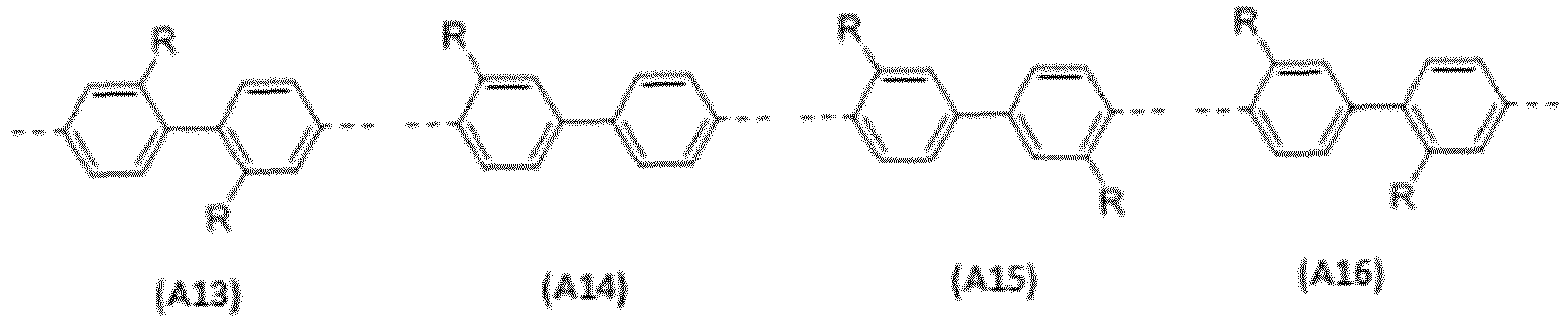


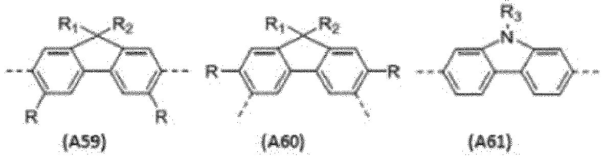


 R = H, R1, R2 ou R3 ;R1, R2 et R3 étant identiques ou choisis indépendamment l'un de l'autre parmi un groupe alkyle linéaire, ramifié ou cyclique comportant 1 à 15 atomes de carbone ; un groupe alcoxy comportant 1 à 15 atomes de carbone ; un groupe aryle comportant 6 à 20 atomes de carbone de cycle ; un groupe hétéroaryle comportant 6 à 20 atomes de cycle ; préférablement un groupe alkyle linéaire, ramifié ou cyclique comportant 1 à 10 atomes de carbone ; un groupe alcoxy comportant 1 à 10 atomes de carbone ; un groupe aryle comportant 6 à 15 atomes de carbone de cycle, un groupe hétéroaryle comportant 6 à 15 atomes de cycle ; en outre de manière préférée un groupe alkyle linéaire, ramifié ou cyclique comportant 1 à 6 atomes de carbone ; un groupe alcoxy comportant 1 à 5 atomes de carbone ; un groupe aryle comportant 6 à 14 atomes de carbone de cycle ; un groupe hétéroaryle comportant 6 à 14 atomes de cycle ; et de manière plus préférée un groupe alkyle linéaire, ramifié ou cyclique comportant 1 à 4 atomes de carbone ; un groupe alcoxy comportant 1 à 2 atomes de carbone ; un groupe aryle comportant 6 à 10 atomes de carbone ; un groupe hétéroaryle comportant 6 à 10 atomes de cycle.
 - OLED (100) selon l'une quelconque des revendications précédentes 1 à 9, ET des formules chimiques Ia, Ib et/ou Ic étant choisi dans un groupe comprenant :- un groupe aryle non substitué comportant 13 à 40 atomes de carbone de cycle ; ou un groupe hétéroaryle non substitué comportant 14 à 40 atomes de cycle, préférablement ET étant choisi dans un groupe comprenant anthracén-2-yle, anthracén-9-yle, pyrén-1-yle, pyrén-2-yle, phénanthrén-9-yle, pérylén-2-yle, pérylén-3-yle, triphénylén-1-yle, triphénylén-2-yle, benzo[f]tetraphén-4-yle, benzo[e]pyrén-4-yle, cyclopenta[cd]fluoranthén-6-yle, benzo[f]tetraphén-10-yle, benzo[e]pyrén-3-yle, chrysène-1-yle, rubicén-5-yle, rubicén-6-yle, fluoranthén-3-yle, dibenzo[j,l]fluoranthén-3-yle, dibenzo[j,l]fluoranthén-9-yle, dibenzo[j,l]fluoranthén-10-yle, benzo[k]tetraphén-1-yle, benzo[k]tetraphén-3-yle, benzo[k]tetraphén-4-yle, benzo[k]tetraphén-7-yle, coronén-1-yle, dibenzo[ghi,mno]fluoranthén-1-yle, dinaptho[2,1-b:1',2'-d]furan-6-yle, acridin-9-yle, dibenzo[c,h]acridin-7-yle ; ou- un groupe aryle substitué comportant 13 à 40 atomes de carbone de cycle ; ou un groupe hétéroaryle substitué comportant 14 à 40 atomes de cycle ; préférablement ET étant choisi dans un groupe comprenant anthracén-2-yle, anthracén-9yle, pyrén-1-yle, pyrén-2-yle, phénanthrén-9-yle, pérylén-2-yle, pérylén-3-yle, dinaptho[2,1-b:1',2'-d]furan-6-yle, acridin-9-yle, dibenzo[c,h]acridin-7-yle, fluorén-2-yle, fluorén-3-yle ;
le substituant du groupe aryle substitué ou du groupe hétéroaryle substitué étant choisi dans un groupe comprenant un groupe phényle, 1-naphtyle, 2-naphtyle, 2-biphényle, 3-biphényle, 4-biphényle, 1-pyrényle, 2-pyrényle, 2-phénanthrényle, 9,9'-fluorényle ou 9,9'-xanthényle. - OLED (100) selon l'une quelconque des revendications précédentes 1 à 10, ET des formules chimiques Ia, Ib et/ou Ic étant choisi dans le groupe de B1 à B32


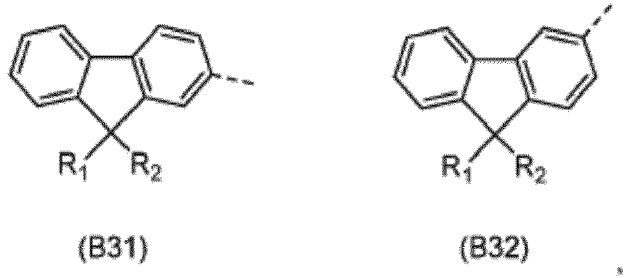
- OLED (100) selon la revendication 11, B1 à B32 étant substitués par un groupe phényle, 1-naphtyle, 2-naphtyle, 2-biphényle, 3-biphényle, 4-biphényle, 1-pyrényle, 2-pyrényle, 2-phénanthrényle, 9,9'-fluorényle ou 9,9'-xanthényle.
- OLED (100) selon l'une quelconque des revendications précédentes 1 à 12,- la deuxième couche de transport d'électrons (162) comprenant au moins un matériau de matrice choisi dans le groupe comprenant :


- OLED (100) selon l'une quelconque des revendications précédentes 1 ou 4 à 13,- la première couche de transport d'électrons (161) comprenant un matériau de matrice choisi dans le groupe comprenant oxyde de 3-(dibenzo[c,h]acridin-7-yl)phényl)diphénylphosphine, oxyde de phénylbis(3-(pyrén-1-yl)phényl)phosphine, 3-phényl-3H-benzo[b]dinaphto[2,1-d:1',2'-f]phosphépine-3-oxyde, oxyde de (3'-(dibenzo[c,h]acridin-7-yl)-[1,1'-biphényl]-4-yl)diphénylphosphine, oxyde de (3-(10-(naphtalén-2-yl)anthracén-9-yl)phényl)diphénylphosphine et/ou 2-(4-(9,10-di(naphtalén-2-yl)anthracén-2-yl)phényl)-1-phényl-1H-benzo[d]imidazole ;- la deuxième couche de transport d'électrons (162) comprenant un matériau de matrice de formule chimique Ia, Ib et/ou Ic ;- l'éventuelle troisième couche de transport d'électrons (163) comprenant un matériau de matrice choisi dans le groupe comprenant 2-(4-(9,10-di(naphtalén-2-yl)anthracén-2-yl)phényl)-1-phényl-1H-benzo[d]imidazole, oxyde de 3-(dibenzo[c,h]acridin-7-yl)phényl)diphénylphosphine, oxyde de phénylbis(3-(pyrén-1-yl)phényl)phosphine, oxyde de (3'-(dibenzo[c,h]acridin-7-yl)-[1,1'-biphényl]-4-yl)diphénylphosphine, oxyde de (3-(10-(naphtalén-2-yl)anthracén-9-yl)phényl)diphénylphosphine et/ou 3-phényl-3H-benzo[b]dinaphto[2,1-d:1',2'-f]phosphépine-3-oxyde ;le matériau de matrice de la deuxième couche de transport d'électrons (162) étant choisi de sorte qu'il soit différent du matériau de matrice de la première couche de transport d'électrons (161) et de l'éventuelle troisième couche de transport d'électrons (163).
- OLED (100) selon l'une quelconque des revendications précédentes 1 à 14, la couche d'injection d'électrons :- comprenant un composé de matrice d'un composé de type oxyde de phosphine substitué par un groupe aryle, hétéroaryle ou alkyle, préférablement 3-phényl-3H-benzo[b]dinaphto[2,1-d:1',2'-f]phosphépine-3-oxyde, et dopé par un halogénure de lithium ou dopé par un complexe organique du lithium préférablement tétra(1H-pyrazol-1-yl)borate de lithium ; ou- comprenant un composé de matrice d'un composé de type oxyde de phosphine substitué par un groupe aryle, hétéroaryle ou alkyle, préférablement oxyde de 3-(dibenzo[c,h]acridin-7-yl)phényl)diphénylphosphine ou 3-phényl-3H-benzo[b]dinaphto[2,1-d:1',2'-f]phosphépine-3-oxyde, et dopé avec un métal élémentaire choisi dans un groupe comprenant des métaux alcalins, alcalino-terreux ou des terres rares, préférablement Li, Cs, Mg, Ca, Yb ou Sm ; ou- étant constituée d'un halogénure métallique ou d'un complexe organométallique, préférablement LiQ, AlQ3, ZrQ4, KF ou LiF, Q étant 8-hydroxyquinoléate ; ou- étant constituée d'un métal alcalin, alcalino-terreux ou des terres rares, préférablement Li, Cs, Mg, Ca, Yb ou Sm.
- Dispositif comprenant au moins une diode luminescente organique (OLED) selon l'une quelconque des revendications précédentes 1 à 14.
Priority Applications (1)
| Application Number | Priority Date | Filing Date | Title |
|---|---|---|---|
| EP21164546.0A EP3872074A1 (fr) | 2015-05-12 | 2016-05-11 | Diode électroluminescente organique comprenant différents composés matriciels dans la première et la seconde couche de transport d'électrons |
Applications Claiming Priority (2)
| Application Number | Priority Date | Filing Date | Title |
|---|---|---|---|
| EP15162788.2A EP3093288A1 (fr) | 2015-05-12 | 2015-05-12 | Diode électroluminescente organique comprenant différents composés matriciels dans la première et la seconde couche de transport d'électrons |
| PCT/EP2016/060582 WO2016180891A1 (fr) | 2015-05-12 | 2016-05-11 | Diode électroluminescente organique comprenant des composés de matrice différents dans les première et deuxième couches de transport d'électrons |
Related Child Applications (2)
| Application Number | Title | Priority Date | Filing Date |
|---|---|---|---|
| EP21164546.0A Division EP3872074A1 (fr) | 2015-05-12 | 2016-05-11 | Diode électroluminescente organique comprenant différents composés matriciels dans la première et la seconde couche de transport d'électrons |
| EP21164546.0A Division-Into EP3872074A1 (fr) | 2015-05-12 | 2016-05-11 | Diode électroluminescente organique comprenant différents composés matriciels dans la première et la seconde couche de transport d'électrons |
Publications (2)
| Publication Number | Publication Date |
|---|---|
| EP3294727A1 EP3294727A1 (fr) | 2018-03-21 |
| EP3294727B1 true EP3294727B1 (fr) | 2021-08-04 |
Family
ID=52814889
Family Applications (3)
| Application Number | Title | Priority Date | Filing Date |
|---|---|---|---|
| EP15162788.2A Withdrawn EP3093288A1 (fr) | 2015-02-18 | 2015-05-12 | Diode électroluminescente organique comprenant différents composés matriciels dans la première et la seconde couche de transport d'électrons |
| EP16722873.3A Active EP3294727B1 (fr) | 2015-05-12 | 2016-05-11 | Diode électroluminescente organique comprenant différents composés matriciels dans la première et la seconde couche de transport d'électrons |
| EP21164546.0A Pending EP3872074A1 (fr) | 2015-05-12 | 2016-05-11 | Diode électroluminescente organique comprenant différents composés matriciels dans la première et la seconde couche de transport d'électrons |
Family Applications Before (1)
| Application Number | Title | Priority Date | Filing Date |
|---|---|---|---|
| EP15162788.2A Withdrawn EP3093288A1 (fr) | 2015-02-18 | 2015-05-12 | Diode électroluminescente organique comprenant différents composés matriciels dans la première et la seconde couche de transport d'électrons |
Family Applications After (1)
| Application Number | Title | Priority Date | Filing Date |
|---|---|---|---|
| EP21164546.0A Pending EP3872074A1 (fr) | 2015-05-12 | 2016-05-11 | Diode électroluminescente organique comprenant différents composés matriciels dans la première et la seconde couche de transport d'électrons |
Country Status (5)
| Country | Link |
|---|---|
| US (1) | US11081652B2 (fr) |
| EP (3) | EP3093288A1 (fr) |
| KR (1) | KR102652730B1 (fr) |
| CN (1) | CN107750404B (fr) |
| WO (1) | WO2016180891A1 (fr) |
Families Citing this family (9)
| Publication number | Priority date | Publication date | Assignee | Title |
|---|---|---|---|---|
| KR102364221B1 (ko) | 2015-03-23 | 2022-02-18 | 삼성디스플레이 주식회사 | 축합환 화합물 및 이를 포함한 유기 발광 소자 |
| KR102458684B1 (ko) * | 2015-10-08 | 2022-10-26 | 삼성디스플레이 주식회사 | 유기 발광 소자 |
| KR101944851B1 (ko) | 2016-09-29 | 2019-02-01 | 엘지디스플레이 주식회사 | 유기 화합물과 이를 포함하는 유기발광다이오드 및 유기발광 표시장치 |
| CN106784355B (zh) * | 2016-12-29 | 2019-10-18 | 深圳市华星光电技术有限公司 | 叠层有机电致发光器件 |
| CN108461638B (zh) * | 2018-02-27 | 2020-06-23 | 上海天马有机发光显示技术有限公司 | 一种有机电致发光器件、其制备方法及显示装置 |
| EP3653619A1 (fr) | 2018-11-16 | 2020-05-20 | Novaled GmbH | Composé, dispositif électronique organique le comprenant, dispositif d'affichage et dispositif d'éclairage le comprenant |
| US20220216428A1 (en) * | 2019-04-15 | 2022-07-07 | Novaled Gmbh | See addendum |
| EP4177978A1 (fr) * | 2021-11-05 | 2023-05-10 | Novaled GmbH | Diode électroluminescente organique, dispositif d'affichage la comprenant et dispositif d'éclairage la comprenant |
| KR20240078109A (ko) * | 2022-11-25 | 2024-06-03 | 엘지디스플레이 주식회사 | 유기발광다이오드 |
Family Cites Families (27)
| Publication number | Priority date | Publication date | Assignee | Title |
|---|---|---|---|---|
| US6800380B2 (en) | 1998-06-23 | 2004-10-05 | Nessdisplay Co., Ltd. | Organometallic luminescent materials and organic electroluminescent device containing same |
| US6225467B1 (en) | 2000-01-21 | 2001-05-01 | Xerox Corporation | Electroluminescent (EL) devices |
| JP3945123B2 (ja) | 2000-04-10 | 2007-07-18 | 三菱化学株式会社 | 有機電界発光素子 |
| JP4876333B2 (ja) | 2000-06-08 | 2012-02-15 | 東レ株式会社 | 発光素子 |
| KR100691543B1 (ko) | 2002-01-18 | 2007-03-09 | 주식회사 엘지화학 | 새로운 전자 수송용 물질 및 이를 이용한 유기 발광 소자 |
| EP2174932B1 (fr) * | 2003-03-13 | 2019-07-03 | Idemitsu Kosan Co., Ltd. | Dérivé hétérocyclique contenant de l'azote et élément électroluminescent organique utilisant ce dérivé |
| JP2007049055A (ja) * | 2005-08-12 | 2007-02-22 | Toyo Ink Mfg Co Ltd | 有機エレクトロルミネッセンス素子用材料および有機エレクトロルミネッセンス素子 |
| EP1786050B1 (fr) | 2005-11-10 | 2010-06-23 | Novaled AG | Matériau semiconducteur organique dopé |
| JP2008195623A (ja) | 2007-02-08 | 2008-08-28 | Chemiprokasei Kaisha Ltd | 新規な複素環含有ヒドロキシフェニル金属誘導体およびそれを用いた電子注入材料、電子輸送材料および有機エレクトロルミネッセンス素子 |
| JPWO2008102740A1 (ja) * | 2007-02-19 | 2010-05-27 | 出光興産株式会社 | 有機エレクトロルミネッセンス素子 |
| DE102007012794B3 (de) | 2007-03-16 | 2008-06-19 | Novaled Ag | Pyrido[3,2-h]chinazoline und/oder deren 5,6-Dihydroderivate, deren Herstellungsverfahren und diese enthaltendes dotiertes organisches Halbleitermaterial |
| EP2372803A4 (fr) * | 2008-12-26 | 2012-07-04 | Idemitsu Kosan Co | Matériau pour élément électroluminescent organique, et élément électroluminescent organique |
| EP2395571B1 (fr) | 2010-06-10 | 2013-12-04 | Novaled AG | Dispositif Électronique organique comprenant un matériau de semiconducteur organique |
| WO2013009095A1 (fr) * | 2011-07-11 | 2013-01-17 | 주식회사 두산 | Composé à base de triphénylène et diode électroluminescente organique l'utilisant |
| KR101474797B1 (ko) * | 2011-08-08 | 2014-12-19 | 제일모직 주식회사 | 유기광전자소자용 화합물 및 이를 포함하는 유기발광소자 |
| KR101914951B1 (ko) * | 2011-08-22 | 2018-11-05 | 메르크 파텐트 게엠베하 | 유기 전계발광 디바이스 |
| EP2750214B1 (fr) | 2011-10-05 | 2020-06-17 | LG Chem, Ltd. | Dispositif électroluminescent organique et son procédé de fabrication |
| WO2013079678A1 (fr) | 2011-11-30 | 2013-06-06 | Novaled Ag | Dispositif électronique organique |
| TWI584513B (zh) | 2011-11-30 | 2017-05-21 | 諾瓦發光二極體有限公司 | 顯示器 |
| CN104067400B (zh) | 2011-11-30 | 2018-02-27 | 诺瓦尔德股份有限公司 | 有机电子器件 |
| KR101908385B1 (ko) * | 2012-03-02 | 2018-10-17 | 삼성디스플레이 주식회사 | 유기 발광 소자 |
| KR102014168B1 (ko) * | 2012-10-12 | 2019-08-27 | 삼성디스플레이 주식회사 | 유기 발광 소자, 이의 제조 방법 및 물질층 형성 방법 |
| CN104884572B (zh) * | 2013-01-03 | 2017-09-19 | 默克专利有限公司 | 用于电子器件的材料 |
| EP2790236B1 (fr) * | 2013-04-10 | 2017-09-20 | Novaled GmbH | Matériau semi-conducteur comprenant une matrice d'oxyde de phosphine d'aza substitué et sel métallique |
| KR101676416B1 (ko) * | 2013-05-31 | 2016-11-15 | 제일모직 주식회사 | 유기 화합물, 유기 광전자 소자 및 표시 장치 |
| KR20140012920A (ko) * | 2013-12-20 | 2014-02-04 | 주식회사 엘지화학 | 신규한 안트라센 유도체 및 이를 이용한 유기전자소자 |
| EP3035400B1 (fr) * | 2014-12-17 | 2019-10-23 | Novaled GmbH | Diode électroluminescente organique comprenant des couches de transport d'électrons avec différents composés matriciels |
-
2015
- 2015-05-12 EP EP15162788.2A patent/EP3093288A1/fr not_active Withdrawn
-
2016
- 2016-05-11 WO PCT/EP2016/060582 patent/WO2016180891A1/fr not_active Ceased
- 2016-05-11 EP EP16722873.3A patent/EP3294727B1/fr active Active
- 2016-05-11 EP EP21164546.0A patent/EP3872074A1/fr active Pending
- 2016-05-11 KR KR1020177034535A patent/KR102652730B1/ko active Active
- 2016-05-11 CN CN201680027228.7A patent/CN107750404B/zh active Active
- 2016-05-11 US US15/572,336 patent/US11081652B2/en active Active
Non-Patent Citations (1)
| Title |
|---|
| None * |
Also Published As
| Publication number | Publication date |
|---|---|
| EP3294727A1 (fr) | 2018-03-21 |
| KR20180005199A (ko) | 2018-01-15 |
| KR102652730B1 (ko) | 2024-03-28 |
| CN107750404A (zh) | 2018-03-02 |
| US11081652B2 (en) | 2021-08-03 |
| US20180145263A1 (en) | 2018-05-24 |
| EP3872074A1 (fr) | 2021-09-01 |
| WO2016180891A1 (fr) | 2016-11-17 |
| CN107750404B (zh) | 2021-06-04 |
| EP3093288A1 (fr) | 2016-11-16 |
Similar Documents
| Publication | Publication Date | Title |
|---|---|---|
| US20240147841A1 (en) | Organic Semiconductive Layer Comprising Phosphine Oxide Compounds | |
| US12161044B2 (en) | Electron transport layer comprising a matrix compound mixture for an organic light-emitting diode (OLED) | |
| EP3294727B1 (fr) | Diode électroluminescente organique comprenant différents composés matriciels dans la première et la seconde couche de transport d'électrons | |
| US11795186B2 (en) | Organic electronic device comprising an organic semiconductor layer and a device | |
| EP3235019B1 (fr) | Diode électroluminescente organique comprenant des couches de transport d'électrons avec différents composés de matrice | |
| KR102826374B1 (ko) | 유기 전계발광 디바이스 | |
| EP3232490B1 (fr) | Diode électroluminescente organique comprenant une couche semi-conductrice organique | |
| KR20200071094A (ko) | 유기 반도체층을 포함하는 유기 전자 소자 | |
| KR102634897B1 (ko) | 트리아진 화합물 및 이를 포함하는 유기 반도전층 | |
| KR20200070309A (ko) | 유기 반도체층을 포함하는 유기 전자 소자 | |
| KR102685005B1 (ko) | 트리아진기, 플루오렌기 및 아릴기를 포함하는 화합물 |
Legal Events
| Date | Code | Title | Description |
|---|---|---|---|
| STAA | Information on the status of an ep patent application or granted ep patent |
Free format text: STATUS: THE INTERNATIONAL PUBLICATION HAS BEEN MADE |
|
| PUAI | Public reference made under article 153(3) epc to a published international application that has entered the european phase |
Free format text: ORIGINAL CODE: 0009012 |
|
| STAA | Information on the status of an ep patent application or granted ep patent |
Free format text: STATUS: REQUEST FOR EXAMINATION WAS MADE |
|
| 17P | Request for examination filed |
Effective date: 20171204 |
|
| AK | Designated contracting states |
Kind code of ref document: A1 Designated state(s): AL AT BE BG CH CY CZ DE DK EE ES FI FR GB GR HR HU IE IS IT LI LT LU LV MC MK MT NL NO PL PT RO RS SE SI SK SM TR |
|
| AX | Request for extension of the european patent |
Extension state: BA ME |
|
| RIN1 | Information on inventor provided before grant (corrected) |
Inventor name: FREY, JULIEN Inventor name: SCHOLZ, JOHANNES Inventor name: ZOELLNER, MIKE Inventor name: DENKER, ULRICH Inventor name: WALLIKEWITZ, BODO Inventor name: GRAEF, KATJA Inventor name: SENKOVSKYY, VOLODYMYR |
|
| DAV | Request for validation of the european patent (deleted) | ||
| DAX | Request for extension of the european patent (deleted) | ||
| STAA | Information on the status of an ep patent application or granted ep patent |
Free format text: STATUS: EXAMINATION IS IN PROGRESS |
|
| 17Q | First examination report despatched |
Effective date: 20190211 |
|
| RAP1 | Party data changed (applicant data changed or rights of an application transferred) |
Owner name: NOVALED GMBH |
|
| GRAP | Despatch of communication of intention to grant a patent |
Free format text: ORIGINAL CODE: EPIDOSNIGR1 |
|
| STAA | Information on the status of an ep patent application or granted ep patent |
Free format text: STATUS: GRANT OF PATENT IS INTENDED |
|
| INTG | Intention to grant announced |
Effective date: 20200731 |
|
| GRAJ | Information related to disapproval of communication of intention to grant by the applicant or resumption of examination proceedings by the epo deleted |
Free format text: ORIGINAL CODE: EPIDOSDIGR1 |
|
| STAA | Information on the status of an ep patent application or granted ep patent |
Free format text: STATUS: EXAMINATION IS IN PROGRESS |
|
| GRAS | Grant fee paid |
Free format text: ORIGINAL CODE: EPIDOSNIGR3 |
|
| STAA | Information on the status of an ep patent application or granted ep patent |
Free format text: STATUS: GRANT OF PATENT IS INTENDED |
|
| INTC | Intention to grant announced (deleted) | ||
| GRAP | Despatch of communication of intention to grant a patent |
Free format text: ORIGINAL CODE: EPIDOSNIGR1 |
|
| GRAJ | Information related to disapproval of communication of intention to grant by the applicant or resumption of examination proceedings by the epo deleted |
Free format text: ORIGINAL CODE: EPIDOSDIGR1 |
|
| GRAS | Grant fee paid |
Free format text: ORIGINAL CODE: EPIDOSNIGR3 |
|
| GRAS | Grant fee paid |
Free format text: ORIGINAL CODE: EPIDOSNIGR3 |
|
| GRAS | Grant fee paid |
Free format text: ORIGINAL CODE: EPIDOSNIGR3 |
|
| GRAJ | Information related to disapproval of communication of intention to grant by the applicant or resumption of examination proceedings by the epo deleted |
Free format text: ORIGINAL CODE: EPIDOSDIGR1 |
|
| GRAP | Despatch of communication of intention to grant a patent |
Free format text: ORIGINAL CODE: EPIDOSNIGR1 |
|
| INTG | Intention to grant announced |
Effective date: 20210112 |
|
| STAA | Information on the status of an ep patent application or granted ep patent |
Free format text: STATUS: EXAMINATION IS IN PROGRESS |
|
| INTC | Intention to grant announced (deleted) | ||
| GRAS | Grant fee paid |
Free format text: ORIGINAL CODE: EPIDOSNIGR3 |
|
| STAA | Information on the status of an ep patent application or granted ep patent |
Free format text: STATUS: GRANT OF PATENT IS INTENDED |
|
| GRAP | Despatch of communication of intention to grant a patent |
Free format text: ORIGINAL CODE: EPIDOSNIGR1 |
|
| INTG | Intention to grant announced |
Effective date: 20210304 |
|
| GRAA | (expected) grant |
Free format text: ORIGINAL CODE: 0009210 |
|
| STAA | Information on the status of an ep patent application or granted ep patent |
Free format text: STATUS: THE PATENT HAS BEEN GRANTED |
|
| AK | Designated contracting states |
Kind code of ref document: B1 Designated state(s): AL AT BE BG CH CY CZ DE DK EE ES FI FR GB GR HR HU IE IS IT LI LT LU LV MC MK MT NL NO PL PT RO RS SE SI SK SM TR |
|
| REG | Reference to a national code |
Ref country code: GB Ref legal event code: FG4D |
|
| REG | Reference to a national code |
Ref country code: AT Ref legal event code: REF Ref document number: 1416868 Country of ref document: AT Kind code of ref document: T Effective date: 20210815 |
|
| REG | Reference to a national code |
Ref country code: CH Ref legal event code: EP |
|
| REG | Reference to a national code |
Ref country code: DE Ref legal event code: R096 Ref document number: 602016061558 Country of ref document: DE |
|
| REG | Reference to a national code |
Ref country code: IE Ref legal event code: FG4D |
|
| REG | Reference to a national code |
Ref country code: DE Ref legal event code: R081 Ref document number: 602016061558 Country of ref document: DE Owner name: NOVALED GMBH, DE Free format text: FORMER OWNER: NOVALED GMBH, 01307 DRESDEN, DE |
|
| REG | Reference to a national code |
Ref country code: LT Ref legal event code: MG9D |
|
| REG | Reference to a national code |
Ref country code: NL Ref legal event code: MP Effective date: 20210804 |
|
| REG | Reference to a national code |
Ref country code: AT Ref legal event code: MK05 Ref document number: 1416868 Country of ref document: AT Kind code of ref document: T Effective date: 20210804 |
|
| PG25 | Lapsed in a contracting state [announced via postgrant information from national office to epo] |
Ref country code: RS Free format text: LAPSE BECAUSE OF FAILURE TO SUBMIT A TRANSLATION OF THE DESCRIPTION OR TO PAY THE FEE WITHIN THE PRESCRIBED TIME-LIMIT Effective date: 20210804 Ref country code: SE Free format text: LAPSE BECAUSE OF FAILURE TO SUBMIT A TRANSLATION OF THE DESCRIPTION OR TO PAY THE FEE WITHIN THE PRESCRIBED TIME-LIMIT Effective date: 20210804 Ref country code: NO Free format text: LAPSE BECAUSE OF FAILURE TO SUBMIT A TRANSLATION OF THE DESCRIPTION OR TO PAY THE FEE WITHIN THE PRESCRIBED TIME-LIMIT Effective date: 20211104 Ref country code: PT Free format text: LAPSE BECAUSE OF FAILURE TO SUBMIT A TRANSLATION OF THE DESCRIPTION OR TO PAY THE FEE WITHIN THE PRESCRIBED TIME-LIMIT Effective date: 20211206 Ref country code: HR Free format text: LAPSE BECAUSE OF FAILURE TO SUBMIT A TRANSLATION OF THE DESCRIPTION OR TO PAY THE FEE WITHIN THE PRESCRIBED TIME-LIMIT Effective date: 20210804 Ref country code: FI Free format text: LAPSE BECAUSE OF FAILURE TO SUBMIT A TRANSLATION OF THE DESCRIPTION OR TO PAY THE FEE WITHIN THE PRESCRIBED TIME-LIMIT Effective date: 20210804 Ref country code: ES Free format text: LAPSE BECAUSE OF FAILURE TO SUBMIT A TRANSLATION OF THE DESCRIPTION OR TO PAY THE FEE WITHIN THE PRESCRIBED TIME-LIMIT Effective date: 20210804 Ref country code: BG Free format text: LAPSE BECAUSE OF FAILURE TO SUBMIT A TRANSLATION OF THE DESCRIPTION OR TO PAY THE FEE WITHIN THE PRESCRIBED TIME-LIMIT Effective date: 20211104 Ref country code: AT Free format text: LAPSE BECAUSE OF FAILURE TO SUBMIT A TRANSLATION OF THE DESCRIPTION OR TO PAY THE FEE WITHIN THE PRESCRIBED TIME-LIMIT Effective date: 20210804 Ref country code: LT Free format text: LAPSE BECAUSE OF FAILURE TO SUBMIT A TRANSLATION OF THE DESCRIPTION OR TO PAY THE FEE WITHIN THE PRESCRIBED TIME-LIMIT Effective date: 20210804 |
|
| PG25 | Lapsed in a contracting state [announced via postgrant information from national office to epo] |
Ref country code: PL Free format text: LAPSE BECAUSE OF FAILURE TO SUBMIT A TRANSLATION OF THE DESCRIPTION OR TO PAY THE FEE WITHIN THE PRESCRIBED TIME-LIMIT Effective date: 20210804 Ref country code: LV Free format text: LAPSE BECAUSE OF FAILURE TO SUBMIT A TRANSLATION OF THE DESCRIPTION OR TO PAY THE FEE WITHIN THE PRESCRIBED TIME-LIMIT Effective date: 20210804 Ref country code: GR Free format text: LAPSE BECAUSE OF FAILURE TO SUBMIT A TRANSLATION OF THE DESCRIPTION OR TO PAY THE FEE WITHIN THE PRESCRIBED TIME-LIMIT Effective date: 20211105 |
|
| PG25 | Lapsed in a contracting state [announced via postgrant information from national office to epo] |
Ref country code: NL Free format text: LAPSE BECAUSE OF FAILURE TO SUBMIT A TRANSLATION OF THE DESCRIPTION OR TO PAY THE FEE WITHIN THE PRESCRIBED TIME-LIMIT Effective date: 20210804 |
|
| PG25 | Lapsed in a contracting state [announced via postgrant information from national office to epo] |
Ref country code: DK Free format text: LAPSE BECAUSE OF FAILURE TO SUBMIT A TRANSLATION OF THE DESCRIPTION OR TO PAY THE FEE WITHIN THE PRESCRIBED TIME-LIMIT Effective date: 20210804 |
|
| REG | Reference to a national code |
Ref country code: DE Ref legal event code: R097 Ref document number: 602016061558 Country of ref document: DE |
|
| PG25 | Lapsed in a contracting state [announced via postgrant information from national office to epo] |
Ref country code: SM Free format text: LAPSE BECAUSE OF FAILURE TO SUBMIT A TRANSLATION OF THE DESCRIPTION OR TO PAY THE FEE WITHIN THE PRESCRIBED TIME-LIMIT Effective date: 20210804 Ref country code: SK Free format text: LAPSE BECAUSE OF FAILURE TO SUBMIT A TRANSLATION OF THE DESCRIPTION OR TO PAY THE FEE WITHIN THE PRESCRIBED TIME-LIMIT Effective date: 20210804 Ref country code: RO Free format text: LAPSE BECAUSE OF FAILURE TO SUBMIT A TRANSLATION OF THE DESCRIPTION OR TO PAY THE FEE WITHIN THE PRESCRIBED TIME-LIMIT Effective date: 20210804 Ref country code: EE Free format text: LAPSE BECAUSE OF FAILURE TO SUBMIT A TRANSLATION OF THE DESCRIPTION OR TO PAY THE FEE WITHIN THE PRESCRIBED TIME-LIMIT Effective date: 20210804 Ref country code: CZ Free format text: LAPSE BECAUSE OF FAILURE TO SUBMIT A TRANSLATION OF THE DESCRIPTION OR TO PAY THE FEE WITHIN THE PRESCRIBED TIME-LIMIT Effective date: 20210804 Ref country code: AL Free format text: LAPSE BECAUSE OF FAILURE TO SUBMIT A TRANSLATION OF THE DESCRIPTION OR TO PAY THE FEE WITHIN THE PRESCRIBED TIME-LIMIT Effective date: 20210804 |
|
| PLBE | No opposition filed within time limit |
Free format text: ORIGINAL CODE: 0009261 |
|
| STAA | Information on the status of an ep patent application or granted ep patent |
Free format text: STATUS: NO OPPOSITION FILED WITHIN TIME LIMIT |
|
| 26N | No opposition filed |
Effective date: 20220506 |
|
| PG25 | Lapsed in a contracting state [announced via postgrant information from national office to epo] |
Ref country code: IT Free format text: LAPSE BECAUSE OF FAILURE TO SUBMIT A TRANSLATION OF THE DESCRIPTION OR TO PAY THE FEE WITHIN THE PRESCRIBED TIME-LIMIT Effective date: 20210804 |
|
| PG25 | Lapsed in a contracting state [announced via postgrant information from national office to epo] |
Ref country code: SI Free format text: LAPSE BECAUSE OF FAILURE TO SUBMIT A TRANSLATION OF THE DESCRIPTION OR TO PAY THE FEE WITHIN THE PRESCRIBED TIME-LIMIT Effective date: 20210804 |
|
| REG | Reference to a national code |
Ref country code: CH Ref legal event code: PL |
|
| REG | Reference to a national code |
Ref country code: BE Ref legal event code: MM Effective date: 20220531 |
|
| GBPC | Gb: european patent ceased through non-payment of renewal fee |
Effective date: 20220511 |
|
| PG25 | Lapsed in a contracting state [announced via postgrant information from national office to epo] |
Ref country code: MC Free format text: LAPSE BECAUSE OF FAILURE TO SUBMIT A TRANSLATION OF THE DESCRIPTION OR TO PAY THE FEE WITHIN THE PRESCRIBED TIME-LIMIT Effective date: 20210804 Ref country code: LU Free format text: LAPSE BECAUSE OF NON-PAYMENT OF DUE FEES Effective date: 20220511 Ref country code: LI Free format text: LAPSE BECAUSE OF NON-PAYMENT OF DUE FEES Effective date: 20220531 Ref country code: CH Free format text: LAPSE BECAUSE OF NON-PAYMENT OF DUE FEES Effective date: 20220531 |
|
| PG25 | Lapsed in a contracting state [announced via postgrant information from national office to epo] |
Ref country code: IE Free format text: LAPSE BECAUSE OF NON-PAYMENT OF DUE FEES Effective date: 20220511 Ref country code: FR Free format text: LAPSE BECAUSE OF NON-PAYMENT OF DUE FEES Effective date: 20220531 |
|
| PG25 | Lapsed in a contracting state [announced via postgrant information from national office to epo] |
Ref country code: GB Free format text: LAPSE BECAUSE OF NON-PAYMENT OF DUE FEES Effective date: 20220511 Ref country code: BE Free format text: LAPSE BECAUSE OF NON-PAYMENT OF DUE FEES Effective date: 20220531 |
|
| P01 | Opt-out of the competence of the unified patent court (upc) registered |
Effective date: 20230526 |
|
| PG25 | Lapsed in a contracting state [announced via postgrant information from national office to epo] |
Ref country code: HU Free format text: LAPSE BECAUSE OF FAILURE TO SUBMIT A TRANSLATION OF THE DESCRIPTION OR TO PAY THE FEE WITHIN THE PRESCRIBED TIME-LIMIT; INVALID AB INITIO Effective date: 20160511 |
|
| PG25 | Lapsed in a contracting state [announced via postgrant information from national office to epo] |
Ref country code: MK Free format text: LAPSE BECAUSE OF FAILURE TO SUBMIT A TRANSLATION OF THE DESCRIPTION OR TO PAY THE FEE WITHIN THE PRESCRIBED TIME-LIMIT Effective date: 20210804 Ref country code: CY Free format text: LAPSE BECAUSE OF FAILURE TO SUBMIT A TRANSLATION OF THE DESCRIPTION OR TO PAY THE FEE WITHIN THE PRESCRIBED TIME-LIMIT Effective date: 20210804 |
|
| PG25 | Lapsed in a contracting state [announced via postgrant information from national office to epo] |
Ref country code: MT Free format text: LAPSE BECAUSE OF FAILURE TO SUBMIT A TRANSLATION OF THE DESCRIPTION OR TO PAY THE FEE WITHIN THE PRESCRIBED TIME-LIMIT Effective date: 20210804 |
|
| PGFP | Annual fee paid to national office [announced via postgrant information from national office to epo] |
Ref country code: DE Payment date: 20250319 Year of fee payment: 10 |
|
| PG25 | Lapsed in a contracting state [announced via postgrant information from national office to epo] |
Ref country code: TR Free format text: LAPSE BECAUSE OF FAILURE TO SUBMIT A TRANSLATION OF THE DESCRIPTION OR TO PAY THE FEE WITHIN THE PRESCRIBED TIME-LIMIT Effective date: 20210804 |