EP3295530B1 - Garniture de câble haute tension et procédé de réalisation d'une garniture de câble haute tension - Google Patents
Garniture de câble haute tension et procédé de réalisation d'une garniture de câble haute tension Download PDFInfo
- Publication number
- EP3295530B1 EP3295530B1 EP16733276.6A EP16733276A EP3295530B1 EP 3295530 B1 EP3295530 B1 EP 3295530B1 EP 16733276 A EP16733276 A EP 16733276A EP 3295530 B1 EP3295530 B1 EP 3295530B1
- Authority
- EP
- European Patent Office
- Prior art keywords
- control part
- field
- fluorophores
- siloxane polymer
- voltage cable
- Prior art date
- Legal status (The legal status is an assumption and is not a legal conclusion. Google has not performed a legal analysis and makes no representation as to the accuracy of the status listed.)
- Active
Links
Images


Classifications
-
- H—ELECTRICITY
- H02—GENERATION; CONVERSION OR DISTRIBUTION OF ELECTRIC POWER
- H02G—INSTALLATION OF ELECTRIC CABLES OR LINES, OR OF COMBINED OPTICAL AND ELECTRIC CABLES OR LINES
- H02G15/00—Cable fittings
- H02G15/02—Cable terminations
- H02G15/04—Cable-end sealings
- H02G15/043—Cable-end sealings with end caps, e.g. sleeve closed at one end
- H02G15/046—Cable-end sealings with end caps, e.g. sleeve closed at one end with bores or protruding portions allowing passage of cable conductors
-
- G—PHYSICS
- G01—MEASURING; TESTING
- G01R—MEASURING ELECTRIC VARIABLES; MEASURING MAGNETIC VARIABLES
- G01R31/00—Arrangements for testing electric properties; Arrangements for locating electric faults; Arrangements for electrical testing characterised by what is being tested not provided for elsewhere
- G01R31/12—Testing dielectric strength or breakdown voltage ; Testing or monitoring effectiveness or level of insulation, e.g. of a cable or of an apparatus, for example using partial discharge measurements; Electrostatic testing
- G01R31/1227—Testing dielectric strength or breakdown voltage ; Testing or monitoring effectiveness or level of insulation, e.g. of a cable or of an apparatus, for example using partial discharge measurements; Electrostatic testing of components, parts or materials
- G01R31/1263—Testing dielectric strength or breakdown voltage ; Testing or monitoring effectiveness or level of insulation, e.g. of a cable or of an apparatus, for example using partial discharge measurements; Electrostatic testing of components, parts or materials of solid or fluid materials, e.g. insulation films, bulk material; of semiconductors or LV electronic components or parts; of cable, line or wire insulation
- G01R31/1272—Testing dielectric strength or breakdown voltage ; Testing or monitoring effectiveness or level of insulation, e.g. of a cable or of an apparatus, for example using partial discharge measurements; Electrostatic testing of components, parts or materials of solid or fluid materials, e.g. insulation films, bulk material; of semiconductors or LV electronic components or parts; of cable, line or wire insulation of cable, line or wire insulation, e.g. using partial discharge measurements
-
- H—ELECTRICITY
- H01—ELECTRIC ELEMENTS
- H01B—CABLES; CONDUCTORS; INSULATORS; SELECTION OF MATERIALS FOR THEIR CONDUCTIVE, INSULATING OR DIELECTRIC PROPERTIES
- H01B3/00—Insulators or insulating bodies characterised by the insulating materials; Selection of materials for their insulating or dielectric properties
- H01B3/18—Insulators or insulating bodies characterised by the insulating materials; Selection of materials for their insulating or dielectric properties mainly consisting of organic substances
- H01B3/30—Insulators or insulating bodies characterised by the insulating materials; Selection of materials for their insulating or dielectric properties mainly consisting of organic substances plastics; resins; waxes
- H01B3/46—Insulators or insulating bodies characterised by the insulating materials; Selection of materials for their insulating or dielectric properties mainly consisting of organic substances plastics; resins; waxes silicones
-
- H—ELECTRICITY
- H02—GENERATION; CONVERSION OR DISTRIBUTION OF ELECTRIC POWER
- H02G—INSTALLATION OF ELECTRIC CABLES OR LINES, OR OF COMBINED OPTICAL AND ELECTRIC CABLES OR LINES
- H02G1/00—Methods or apparatus specially adapted for installing, maintaining, repairing or dismantling electric cables or lines
- H02G1/14—Methods or apparatus specially adapted for installing, maintaining, repairing or dismantling electric cables or lines for joining or terminating cables
-
- H—ELECTRICITY
- H02—GENERATION; CONVERSION OR DISTRIBUTION OF ELECTRIC POWER
- H02G—INSTALLATION OF ELECTRIC CABLES OR LINES, OR OF COMBINED OPTICAL AND ELECTRIC CABLES OR LINES
- H02G15/00—Cable fittings
- H02G15/02—Cable terminations
-
- H—ELECTRICITY
- H02—GENERATION; CONVERSION OR DISTRIBUTION OF ELECTRIC POWER
- H02G—INSTALLATION OF ELECTRIC CABLES OR LINES, OR OF COMBINED OPTICAL AND ELECTRIC CABLES OR LINES
- H02G15/00—Cable fittings
- H02G15/02—Cable terminations
- H02G15/06—Cable terminating boxes, frames or other structures
- H02G15/064—Cable terminating boxes, frames or other structures with devices for relieving electrical stress
- H02G15/068—Cable terminating boxes, frames or other structures with devices for relieving electrical stress connected to the cable shield only
-
- H—ELECTRICITY
- H02—GENERATION; CONVERSION OR DISTRIBUTION OF ELECTRIC POWER
- H02G—INSTALLATION OF ELECTRIC CABLES OR LINES, OR OF COMBINED OPTICAL AND ELECTRIC CABLES OR LINES
- H02G15/00—Cable fittings
- H02G15/08—Cable junctions
- H02G15/18—Cable junctions protected by sleeves, e.g. for communication cable
- H02G15/184—Cable junctions protected by sleeves, e.g. for communication cable with devices for relieving electrical stress
-
- H—ELECTRICITY
- H01—ELECTRIC ELEMENTS
- H01B—CABLES; CONDUCTORS; INSULATORS; SELECTION OF MATERIALS FOR THEIR CONDUCTIVE, INSULATING OR DIELECTRIC PROPERTIES
- H01B9/00—Power cables
- H01B9/006—Constructional features relating to the conductors
-
- H—ELECTRICITY
- H02—GENERATION; CONVERSION OR DISTRIBUTION OF ELECTRIC POWER
- H02G—INSTALLATION OF ELECTRIC CABLES OR LINES, OR OF COMBINED OPTICAL AND ELECTRIC CABLES OR LINES
- H02G15/00—Cable fittings
- H02G15/003—Filling materials, e.g. solid or fluid insulation
Definitions
- the present invention relates to a high voltage cable assembly, in particular a cable sleeve and an end closure, and an associated manufacturing method.
- a polymeric insulating material changes in the high voltage alternating field in several stages.
- the processes that lead to partial discharges in dielectrics under DC voltage loading could be similar in the following but not described in detail.
- high voltage AC fields are based on a three-stage phenomenological aging model of polymeric insulations, which includes the partial discharge process as the third stage.
- charge carriers which, depending on the material and field distribution, are characterized by a characteristic critical field strength. This process can take place in insulating material wherever the critical field strength is exceeded due, for example, to production-related inhomogeneities. But it can also take place at the interface to the live conductor.
- the second model stage is characterized in that with the beginning of the charge carrier injection, an energy transfer from the electric field via the injected charge carriers to the polymer matrix takes place.
- Material-dependent and production-related inhomogeneities play a central role in this, since they serve as starting points for the irreversible damage mechanisms that are now beginning.
- the charge carrier injection in the respective vibrations of the high voltage alternating field leads to a space charge buildup in traps. This can lead to electroluminescence phenomena.
- the occurrence of electroluminescence in this phase can be caused by so-called "hot electron” processes, by excitation of molecules, and by charge carrier recombinations. Which of these processes may dominate depends on the material.
- the energy transfer via the injected charge carriers leads to irreversible chemical, mechanical and thermal changes of the polymer structure.
- the local field strength course is typically strongly influenced by space charge reactions. Subsequently, it may lead to the formation of micro-cavities, which may be associated with the emission of acoustic signals and ignite in which after exceeding a critical size partial discharges, whereby the third stage is reached. Electrochemical changes (reaction shrinkage) and / or during the partial discharges can also cause mechanical stresses to develop, as a result of which cracks and crevices form in the insulating material. As the process progresses, more and more partial discharges can occur, which can lead to growing partial discharge trees and finally to the unwanted electrical breakdown and the aforementioned serious consequential damage.
- Partial discharges can be detected by fiber optic methods. This is how the document describes US 7,668,412 B2 a method and a distributed detection system for detecting discharges and for monitoring electrical lines.
- an optical fiber with a silica core of less than 500 micrometers in diameter and a cladding, in which a luminescent material is integrated brought in the vicinity of objects to be examined.
- a photodetector is positioned at a second end of the optical fiber and receives and measures both a direct emission light from a partial electrical discharge event and the emission light reflected from a first reflective end of the optical fiber. The measured signals and their arrival times are used to determine the location and size of a partial electrical discharge.
- DE 10 2010 061 607 A1 a method for monitoring aging processes of insulation in a high voltage device.
- the method comprises measuring a light signal generated in the insulation with a first fiber optic sensor and measuring a mechanical size of the insulation with a second fiber optic sensor based on fluorophore-doped optical fibers, and estimating an aging state of the insulation.
- the describes DE 10 2010 061 607 A1 a high voltage device with a transparent or translucent insulation and a fiber optic sensor based on fluorophore-doped optical fibers and a second fiber optic sensor for detecting deformations.
- the present invention proposes a high voltage harness according to claim 1, a method according to claim 12 and a use according to claim 15.
- a high voltage harness for receiving a high voltage cable having a conductive electrical conductor and a cable insulation surrounding the conductor comprises insulation and a waveguide.
- the insulation comprises an at least partially transparent or translucent field control member comprising a siloxane polymer, typically a siloxane elastomer (elastomeric field control member), more typically a silicone elastomer.
- the siloxane polymer has fluorophores which are covalently coupled to the siloxane polymer and / or dielectric pigments embedded in the siloxane polymer and / or dielectric pigments at least in a subarea of the field control part.
- the field control part is set up to at least partially surround the cable insulation of the high-voltage cable.
- the waveguide is arranged so that at least one light signal caused by a partial discharge in the field control part can couple from the field control part into the waveguide.
- the high voltage harness is a cable gland or cable termination.
- high voltage is intended to include voltages above about 1 kV, in particular, the term high voltage is the usual average voltage ranges in the energy transfer medium voltage from about 3 kV to about 50 kV, the high voltage of about 50 kV to about 110 kV as well as maximum voltages up to now about 500 kV. In the event that the cable operating voltages are further increased, these voltage ranges should also be included. These can be DC voltages as well as AC voltages.
- high voltage cable is intended to describe a cable that is capable of handling high current, i. electric current of more than about one ampere at voltages above about 1 kV. In the following, the terms high voltage cable and power cable are used synonymously. Accordingly, the term “high voltage cord” or “high voltage harness” is intended to describe a device capable of interconnecting high voltage cables with high voltage equipment and / or high voltage cables with overhead power lines and / or high voltage cables
- the light signals coupled into the waveguide may be coupled to an optical detector, e.g. a photocell or a spectrometer in a control station forwarded.
- an optical detector e.g. a photocell or a spectrometer in a control station forwarded.
- a high-voltage device comprises a high-voltage cable set with a field control part based on a siloxane polymer which has fluorophores and / or dielectric pigments in at least one partial area, wherein the fluorophores can be covalently coupled to the siloxane polymer and / or to the dielectric pigments embedded in the siloxane polymer Waveguide arranged so that a light signal generated in the field control part from the field control part can couple into the waveguide and an optical detector coupled to the waveguide of the high voltage cable set.
- the high voltage device may comprise a plurality of such high voltage cable sets.
- the high-voltage device further comprises a control and evaluation unit coupled to the optical detector, which typically forms a monitoring device for high-voltage cable fittings, and / or a light source connected to the control and evaluation unit, which is located within a housing of the high-voltage cable set, typically in a low-electrical range Field strength during operation of one or two cables connected high-voltage cable set, is arranged.
- the light source eg an LED, can serve to check the functionality of the sensor formed by the waveguide and the optical detector for the light signals caused by damage processes in the insulation.
- the optical radiation (light signal) emitted and to be detected by the damage processes can result both from electroluminescence (in particular in areas of high electric field strength in the field control part) and photoluminescence processes, in particular wavelength ranges as well as from partial discharge processes in the developing discharge trees.
- partial discharge as used herein is intended to describe short term, relatively low energy and localized discharges in the insulation that do not immediately lead to electrical breakdown but irreversibly damage the material of the insulation.
- partial discharge is intended to cover in particular the term “partial internal discharge", i. an externally not necessarily visible discharge phenomena in non-gaseous insulating materials, in particular in solid insulating materials such as polymers include. Starting from imperfections, such as cavities and foreign inclusions or interfaces to other materials, especially to high-voltage conductors, partial discharges can lead to growing over time Crystalentladungsbäumchen in the insulating material, which can eventually lead to breakdown. Partial discharge trees typically have a size greater than about 1 micron (microns).
- the waveguide can be arranged in the field control part and / or on a surface of the field control part.
- the waveguide is an optical fiber, more typically a polymeric optical fiber (POF), which may be the siloxane polymer of the field control member or other siloxane polymer.
- PPF polymeric optical fiber
- the optical fiber can have a fluorescence-doped fiber core at least in a fiber section which is arranged on or in the field control part. This enables a particularly efficient coupling of light from the field control part into the optical fiber and a low-loss transmission of the coupled-in light.
- the waveguide may also be modified in its cladding and / or in its core with covalently bonded fluorophores.
- the field control part fluorophores are selected to convert the light signal caused by damage processes into radiation of a wavelength range in which the siloxane polymer has higher transparency than in the wavelength range of the original (primary) light signal.
- the fluorophores of the field control part may be in a wavelength range below 500 nm, e.g. in the UV range, and re-emit longer wavelength light according to their Stokes shift, which is less absorbed by the siloxane polymer.
- Naphtalimide dyes for example, which can be covalently bonded via corresponding reactive groups to the polymer network, typically a silicone elastomer network, can be used as fluorophores.
- Fluorophores can be covalently bound to monomeric siloxane units, but also to crosslinkable oligomeric siloxanes. However, other radicals such as fused aromatics, fluorinated hydrocarbons or aliphatic hydrocarbons are possible to which fluorophores can be covalently bonded.
- the mass fraction of the covalently linked fluorophores in the partial region of the field control part or the entire field control part based on the siloxane is a function of the absorption cross-sections, typically at least 5 ppmw and may be up to about 500 ppmw (ppmw of English "parts per million by weight", equivalent to 10 6 * Mass fluorophore / mass Siloxane). This allows a sufficiently good conversion and subsequent transmission of the light signal caused by damage processes in the field control part.
- the siloxane polymer may be modified with various covalently bonded fluorophores which are FRET pairs (Förster resonance energy transfer pairs). Act.
- a silicone polymer may be doped with naphthalene and dansyl, naphthalimide and diethylaminocoumarin, or fluorescein and rhodamine.
- two molecules of the FRET pair will be bound by covalent attachment to the siloxane network by appropriate synthesis steps to a common (optically and in terms of the electron systems of the fluorophore molecules passive) carrier molecule that their spatial distance permanently to a value within the FRET radius is limited from about 30 to 70 angstroms.
- the fluorophores are covalently coupled to the siloxane polymer or to dielectric particles embedded in the siloxane polymer, which in turn may be covalently bonded to the siloxane polymer.
- the dielectric particles may be functionalized particles, typically nanoparticles.
- hydridosiloxane surface functionalized silica particles or polyorganosiloxane particles having unsaturated functionalities eg, hydrido groups or unsaturated hydrocarbon groups such as allyl and vinyl groups
- unsaturated functionalities eg, hydrido groups or unsaturated hydrocarbon groups such as allyl and vinyl groups
- Covalent coupling of the fluorophores prevents diffusion of the fluorophores in the siloxane polymer. This allows the fluorophores to remain in the subdomain during the prospected life of up to several decades, e.g. in particularly vulnerable sub-areas or as sub-areas serving light-carrying areas.
- the field control part typically occupies that space in the high voltage trim in which the field strength in high voltage operation is too large for the remainder of the isolation.
- the field control part which is also referred to as a field control body, a conductive deflector for changing the electric field profile in the high-voltage fitting, which is contactable with a cable shielding of the high-voltage cable.
- the field control part can be designed, in particular, as a field control cone with an integrated conductive deflector.
- the field control part can lead the field lines in the high-voltage operation of the high-voltage cable set so that the field strength outside the field control part is sufficiently low.
- the conductive deflector can have a high absorption coefficient in the expected wavelength range of the electroluminescent appearance and / or partial discharge phenomenon due to intercalated graphite or soot particles and then represents a substantially non-transparent or strongly absorbing part of the field control part.
- the deflector may consist of the siloxane polymer of the remainder of the field control member or other siloxane polymer.
- the siloxane polymer of the deflector may also be modified with covalently bonded fluorophores and / or have dielectric pigments, for example in the edge region to the remaining part of the field control part. Thereby, a part of the light signal can be prevented from entering the more absorbing deflector.
- the field control part has a plurality of disjoint or even spaced-apart fluorophores and / or dielectric pigments having partial regions. In this way, a particularly high proportion of the light signal caused or accompanied by damage processes in the field control part can be coupled into the waveguide.
- the primary light signal caused or accompanied by damage processes in the field control part can be converted in a first subarea by its fluorophores into a longer wavelength secondary light signal that is reflected by the pigments of a second subarea and thereby at least partially prevented from penetrating into the absorbing deflector Leaving the field control part is prevented in the direction of a non-polymeric further insulating region and / or at least partially deflected in the direction of the waveguide.
- the field control part can have several subareas with fluorophores and / or several subareas with pigments, but also only one subarea with fluorophores or only one subarea with pigments.
- sub-region (s) are three-dimensional regions. If the concentration of the fluorophores or pigments in the sub-area (s) is very high, they may also be very thin, eg in comparison to the dimensions of the field control part practically a typically curved area (ie a thin layer with high surface / volume ratio) represent, which may be arranged near a surface of the field control part, and / or forms a part of the surface.
- the reflectivity of the dielectric pigments is greater than 0.8, more typically greater than 0.9, to reflect as much light as possible in desired directions. Therefore, the dielectric pigments are typically white.
- particles of TiO 2 , ZnO, SnO, or Al 2 O 3 or dielectric particles with coatings of these materials can serve as dielectric pigments.
- the concentration of the dielectric pigments in the sub-area is higher than 1% vol., More typically higher than 2% vol., And even more typically higher than 5% vol. As a result, a sufficiently high proportion of the light can be reflected.
- the shape and arrangement of the sub-region or the sub-regions and the waveguide or the waveguide are coordinated with each other in order to achieve a particularly good light transmission and thus high measurement sensitivity.
- the method is carried out in such a way that the siloxane polymer has fluorophores and / or dielectric pigments at least in a subarea of the field control part, and that at least one light signal caused by a partial discharge in the field control part can couple from the field control part into the waveguide.
- forming the field control part involves mixing the crosslinkable components of an often two-component siloxane system with those functionalized for crosslinking Fluorophores, fluorophors attached to dielectric particles, and / or the dielectric pigments to form a mixture, incorporating the mixture into the mold, and polymerizing the mixture in the mold.
- the field control part to be produced typically has regions which are free or at most slightly modified with covalently bonded fluorophores and dielectric pigments, siloxane without fluorophores and dielectric pigments is also typically introduced into the mold.
- the process may also be iterative.
- the field control part comprises several cycles of introducing the mixture or siloxane and then polymerizing the mixture in the mold.
- the dielectric pigments may alternatively or additionally be applied to a surface or surface portion of the mold prior to introduction of the mixture, or as a paint after removal of the polymerized siloxane from the mold, eg, by applying a white silicone resin paint, ie, a silicone resin based paint with white dielectric Particles, such as TiO 2 particles.
- a white silicone resin paint ie, a silicone resin based paint with white dielectric Particles, such as TiO 2 particles.
- a section of the waveguide can be introduced into the mold.
- the waveguide may also be applied only on a surface of the field control part after it has been formed in the mold, e.g. glued with and / or on the surface by means of a silicone adhesive.
- the deposited waveguide may then be provided with a siloxane-based reflective layer, e.g. by applying a corresponding silicone resin paint. As a result, light losses can be further reduced. These steps can also be done on site.
- a siloxane polymer having fluorophores and / or dielectric pigments is used as insulation of a high voltage device.
- Damage or aging processes of the insulation can be monitored in a highly sensitive and reliable manner via at least one waveguide optically coupled to the insulation and an optical detector coupled to the at least one waveguide.
- the high-voltage device is typically a high-voltage cable set, in particular a cable sleeve or a cable end closure, the field control part of which typically comprises subregions of the fluorophore and / or siloxane polymer having dielectric pigments.
- siloxane polymer modified with covalently bonded fluorophores and / or dielectric pigments can also be used as insulation in other high voltage devices such as voltage transformers (transformers) and switchgear.
- a high-voltage device comprises an at least partially transparent or translucent insulation based on a siloxane polymer, wherein the siloxane polymer at least in a part of the isolation fluorophores and / or dielectric pigments, and a waveguide, which is arranged so that at least one by a partial discharge in the insulation caused light signal from the insulation in the waveguide can couple.
- Fig. 1 shows a high-voltage fitting 100 for receiving a high-voltage cable 1 according to an embodiment in a schematic central cross-sectional view along the cylinder axis of the high voltage cable 1.
- the rotationally symmetrical high voltage cable 1 inside a conductor 11 for conducting high current, for example.
- An aluminum or copper conductor, of a Cable insulation 12, typically a VPE insulation (cross-linked polyethylene), and an outer cable shield 13, for example, an outer conductive layer or a semiconductive outer cable shield is surrounded.
- the high-voltage cable 1 may additionally comprise cushioning layers and a copper screen and an outer jacket for protection against environmental influences. This may be a polyethylene jacket or a jacket of another halogen-free material.
- the high voltage cable 1 may have an inner conductive layer between the conductor 11 and the XLPE insulation. This inner conductive layer is also not shown.
- the cable end closure 100 represents a cable end 100, as used for example in overhead lines.
- the cable end closure 100 has a housing 110, eg a ceramic housing, which seals off the inner parts of the high voltage fitting 100 from the environment.
- the housing 110 encloses (apart from openings, for example for the high-voltage cable 1) typically a cross-sectionally axially symmetrical, for example cylindrically symmetrical interior.
- an insulating region 3 is arranged in the interior (interior) of the housing 110.
- the insulating region 3 can be formed, for example, by a largely transparent insulating space filled with oil or gas.
- the outer layers are removed, which typically continues the semiconductive outer cable shielding 13 into the area of the field control part and then continued through the end cap through to the head fitting only the cable insulation 12 with the conductor 11 axially. Only the conductor 11 is completely passed through the cable end 100 to be in the right area of FIG. 1 after leaving the cable end 100 to be connected to the overhead line. Inside the cable end closure 100, the conductor 11 is surrounded directly by the insulating area 2 only in the area of the removed cable insulation.
- a rotationally symmetrical electrically insulating field control part 2 is inserted into the interior of the housing 110, which occupies that part of the interior in which the electric field strength would be too large for the insulating materials in the isolation area 3.
- the field control part 2 has an inner hollow cylinder, in which the high voltage cable 1 can be inserted.
- the field control part 2 can be designed as a field control cone.
- the field control part 2 is an elastomeric field control part which at least partially consists of a transparent or translucent elastomeric body, e.g. of a silicone elastomer body with sufficiently high transparency at one or more wavelengths from a range of about 300 nm to about 900 nm.
- the inner hollow cylinder is typically dimensioned such that there is a press fit between the cable insulation 12 of the inserted cable 1 and the field control part 2 Field control part 2 thus forms a stress cone.
- the non-polymeric insulating region 3 and the field control part 2 together form the insulation 2, 3 of the cable end closure 100.
- the field control part 2 and / or the high-voltage cable 1 can additionally be fixed, for example via springs, to the housing 110 or in a ground-level (at least almost field-free) cable-near region 5 of the isolation region 3, e.g. when the isolation region 3 is formed by a solid insulating body.
- Such fixation of field control part 2 and / or high voltage cable 1 is typically used in a construction of the cable end closure 100 in component construction.
- a cable sleeve (not shown) has two field control parts for receiving one of two cables to be connected with partially removed cable insulation and for the suitable guidance of the field lines in the high-voltage operation of the high-voltage cable set.
- an elastomeric field control part 2 is used, in which a suitably shaped conductive deflector 4 is integrated.
- the conductive deflector 4 is in electrical contact with the cable shield 13.
- the conductive deflector 4 also made of a silicone elastomer, but by doping, for example with carbon, has a suitable electrical conductivity.
- a waveguide 51 leads into the interior of the high-voltage fitting 100 into the field control part 2, in which it forms several turns 51w near the surface of the field control part 2.
- the waveguide 51 is thus partially embedded in the field control part 2. Since the waveguide 51 is disposed in a low field intensity region during operation (shielded from the region 8 by the deflector), any moderate differences in the effective dielectric constant of the waveguide 51 have only a small influence on the dielectric constant of the material of the field control part 2 (siloxane) the field course in high voltage operation.
- the probability of coupling a high-voltage-field-induced and charge-carrier-mediated change process (damage process) in the field control part 2 to the primary light signal into the waveguide 51 can be increased.
- the detection probability for the damage process can be increased by means of an optical detector coupled to the waveguide.
- the detection probability for the damage process can also be increased by the in the exemplary embodiment hollow frustum portion 2a of the field control part 2, since silicone elastomer of the field control part 2 is modified in the sub-area 2a with covalently bonded fluorophores, the most likely in area 8 resulting primary light signal in a longer-wave secondary Convert light signal that is less strongly absorbed.
- the non-directional emission of photons from the fluorophor leads to a reduction in the proportion of light that leaves the field control part 2 in the isolation region 3.
- the waveguide 51 is typically a fluorescent optical fiber (FOF), more typically a polymeric doped-core fluorescent polymer optical fiber.
- FOF fluorescent optical fiber
- the absorption wave spectrum is of the fluorophore matched to the expected spectrum of the light signals in the field control part 2. This can provide an extremely sensitive sensor for the light signals.
- the core of the FOF has both fluorophores with an absorption spectrum tuned to the primary light signal and fluorophores with an absorption spectrum tuned to an emission spectrum of the fluorophores of the subarea 2a (multiply doped core of the FOF).
- the fluorophores of subregion 2a can absorb light from a subregion of the wavelength range from 280 nm to 500 nm, more typically from 315 nm to 500 nm and more typically from 350 nm to 500 nm, and longer wavelength (secondary) light in the wavelength range above 500 nm, eg in the range of 500 nm to 800 nm, typically in a portion thereof where the fluorophores of the core absorb the FOF.
- the emission spectrum of the fluorophores of subregion 2a typically has a strong overlap with the absorption spectrum of the fluorophores of the core of the FOF. It is also possible to use multiple fluorophores and create an energy gradient.
- the use of suitably geometrically fixed fluorescent dye pairs is possible, which enable a radiationless and thus lossless energy transfer (FRET pairs).
- the effective dielectric constant of the optical fiber 51 deviates from that of the field control part 2, a change in the electric field distribution in the insulation may occur. Then it may additionally be provided that the shape and / or conductivity of the field control part 2, in particular of the deflector is modified so that the change in the electric field is compensated by the optical fiber 51. However, a change in the electric field distribution can also be largely avoided, at least if the optical fiber 51 is also based on a siloxane.
- the fluorescent optical fiber 51 typically forms, together with an unillustrated optical detector, a so-called "FOF sensor", i. that the detector is tuned to an emission wave spectrum of the fluorophore (or the fluorophore) of the doped core.
- FOF sensor a so-called “FOF sensor”
- Both cladding and core of the light-fiber may also be modified with covalently bonded fluorophores.
- At least one end of the fluorescent optical fiber 51 is connected to the optical detector (optically coupled). However, both ends of the fluorescent optical fiber 51 may be connected to the optical detector. This can be a special high sensitivity can be achieved.
- the optical detector is typically an opto-electrical converter, for example a photodiode, for example an avalanche photodiode, or else a photomultiplier or even a spectrometer.
- the optical detector and an evaluation unit connected to it are typically located in a field-free space 5 or outside of the end closure housing 110.
- the detector and evaluation unit can be largely protected against electromagnetic disturbances of the high-voltage field.
- the evaluation unit can even be a control and evaluation unit.
- the fluorescent optical fiber 51 can be guided directly to the evaluation unit. But it is also possible to connect the fluorescent optical fiber 51 via a transport optical fiber with lower attenuation to the evaluation unit.
- a fluorescent optical fiber 51 having a tuned absorption wavelength region but a plurality of different absorption wavelength regions in the field control part.
- a broader section of the emission spectrum of partial discharges and / or electroluminescence can be detected with high sensitivity.
- Each of these fluorescence optical fibers can be coupled to an individual detector, e.g. a matched to the respective fluorophore individual photodiode are connected. The signals of the individual photodiodes can then be simply added, for example, in order to determine an integral measure of the light output.
- the conductive deflector 4 may be intransparent due to its doping. In this case, the deflector shadows as if Fig. 1 As can be seen, the fluorescent optical fiber 51 optically at least partially from the area 8 with increased field strength. Due to the fluorescence-doped subarea 2a, primary light signals emanating from region 8 can still be detected via secondary light signals.
- the sub-area 2a may also be doped with pigments in place of the fluorophores, which reflect well the primary light signals, such as titanium oxide particles. Even so, the shading effect of an intransparent or strongly absorbing deflector 4 can at least partially be compensated.
- the subarea 2a has a fluorescence-doped inner part (inner ring, due to the axis symmetry, the subregion is typically substantially annular) and a pigmented outer part (outer ring). With this arrangement, a particularly large amount of light power from the field control part can be coupled into the optical fiber 51.
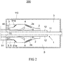
- Fig. 2 shows a high voltage fitting 200 for receiving a high voltage cable 1 according to an embodiment in a schematic central cross sectional view along the cylinder axis of the high voltage cable 1.
- the high voltage fitting 200 is similar to the reference to Fig. 1
- the optical fiber 51 of the cable end closure 200 is not embedded in the field control part 2, but arranged on its outer surface, for example glued to it. Even with this arrangement, high-voltage field-induced aging processes can be detected with high sensitivity.
- a light source 40 e.g. a LED, which is connected to the control and evaluation unit and can be used by this for checking and / or calibration of the fiber optic sensor.
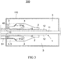
- Fig. 3 shows a high voltage 300 for receiving a high voltage cable 1 according to an embodiment in a schematic central cross sectional view along the cylinder axis of the high voltage cable 1.
- the high voltage 300 is similar to the reference to Fig. 1 High voltage fitting 100 and also represents a cable termination.
- the field control part 2 of the cable end closure 200 is, however, with the exception of the deflector 4 of a fluorophores doped siloxane elastomer, for example of a doped with fluorophores silicone elastomer.
- the field control part 2 of the cable end cap 200 can be made relatively easily, since apart from the deflector 4 only a fluorophore-added siloxane is needed.
- the region 8 with increased field strength doped with fluorophores. Therefore, the primary light signals occurring in the area 8 of the highest risk for field-induced aging processes can be efficiently converted into longer-wavelength secondary light signals and the measurement sensitivity can be increased due to the lower absorption losses of the secondary light signals.
- the field control part 2 has a hollow cone-shaped, doped with fluorophores subregion 2a, which includes the area 8 of the highest risk for field-induced aging processes for the most part.
- That the area 8 partially or completely sub-area 2a can alternatively to the in Fig. 4 geometry shown to be hollow cylindrical and extend, for example, to or close to the cable insulation 12.
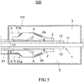
- Fig. 5 shows a high voltage 500 for receiving a high voltage cable 1 according to an embodiment in a schematic central cross-sectional view along the cylinder axis of the high voltage cable 1.
- the high voltage 500 is similar to the reference to Fig. 1 High voltage fitting 100 and also represents a cable termination.
- the sub-area 2a of the field control part 2 of the cable end cap 500 is not doped with fluorophores but with dielectric pigments. Due to the reflection of the primary light signals emanating in particular from the region 8 on the dielectric pigments of the subarea 2a, the proportion of the primary light signal coupled into the optical fiber 51 can be increased.
- the sub-area 2a forms a reflective layer.
- the optical fiber 51 is arranged only on the surface of the field control part 2. This makes it possible to install or retrofit the optical fiber 51 on site.
- the optical fiber 51 of the cable end cap 500 may also be as above with respect to Fig. 1 partially explained embedded in the field control part 2. Due to the defined production conditions, a smaller fluctuation of the sensitivity for the measurement of field-induced aging processes can be expected.
- the optical fiber 51 is partially embedded in the field control part 2, light losses can be further reduced by a (further) reflective layer portion of the field control part 2 with dielectric pigments disposed behind the turns 51w as viewed from the region 8.
- Fig. 6 shows a high-voltage fitting 600 for receiving a high-voltage cable 1 according to an embodiment in a schematic central cross-sectional view along the cylinder axis of the high voltage cable 1.
- the high voltage fitting 600 is similar to the high voltage 100 and also represents a cable termination Field control part 2 of the cable end closure 600, however, two optical fibers 51, 52 (or even more than two optical fibers) are embedded and arranged circumferentially.
- the optical fibers 51, 52 are guided to the part doped with fluorophores 2a, or at least to close to the sub-area 2a. With this arrangement, aging processes caused by high voltage fields can be detected particularly sensitively via the associated light signals.
- Fig. 7 shows a high voltage 700 for receiving a high voltage cable 1 according to an embodiment in a schematic central cross-sectional view along the cylinder axis of the high voltage cable 1.
- the high voltage 700 is similar to the reference to Fig. 6
- the optical fibers 51, 52 of the cable termination 700 do not lead to the sub-area 2a, but only up to a further sub-area 2b, which is also with fluorophores.
- the fluorophores of subregion 2a typically absorb light from a portion of the wavelength range of 280 nm to 500 nm, more typically from 315 nm to 500 nm, and even more typically from 350 nm to 500 nm, and longer wavelength (secondary) light in the wavelength range above 500 nm, eg emit in the range of 500 nm to 800 nm, typically in a partial area thereof, in which the fluorophores of the further sub-area 2a and possibly also the fluorophores of the core of the optical fibers 51, 52 absorb well.
- the emission spectrum of the fluorophores of the subarea 2a typically has a strong overlap at least with the absorption spectrum of the fluorophores of the subarea 2b.
- the sub-area 2a of the cable termination 700 may also be used as a reflective sub-area, i. be formed as doped with dielectric pigments sub-area.
- a plurality of fluorescent optical fibers are in each case embodied as a half loop and embedded in the field control part with a collecting fiber which acts as a "slip ring" doped with a further fluorophore.
- the collecting fiber on the side facing away from the half-loop side with a white, reflective layer; For example, a TiO 2 particles or ZnO particles containing layer coated.
- the Lichteinkoppeleffizienz can be further increased.
- the high-voltage devices described herein have an at least partially transparent or translucent insulation based on a siloxane polymer, typically based on a silicone elastomer, wherein the siloxane polymer has at least in a part of the isolation fluorophores and / or dielectric pigments, and a waveguide, typically an optical fiber with a fluorescence-doped fiber core, which is arranged so that a resulting in the insulation light signal from the insulation can couple into the waveguide.
- the light signal generated in the insulation may, for example, be a partial discharge flash or be caused by an electrically induced change process of the insulation preceding the partial discharge, e.g. an electroluminescent signal.
- the fiber-optic measurement enables a simpler and / or more sensitive and / or earlier detection of high-voltage field-induced aging processes in the insulation.
- the detection sensitivity of high voltage field induced aging processes in the insulation can be significantly increased.
Landscapes
- Physics & Mathematics (AREA)
- Spectroscopy & Molecular Physics (AREA)
- General Physics & Mathematics (AREA)
- Investigating, Analyzing Materials By Fluorescence Or Luminescence (AREA)
- Testing Relating To Insulation (AREA)
- Photo Coupler, Interrupter, Optical-To-Optical Conversion Devices (AREA)
Claims (16)
- Garniture de câble à haute tension (100-700) destinée à accueillir un câble à haute tension (1, 22) comprenant un conducteur (11, 112) conçu pour conduire du courant électrique et un isolant de câble (12, 122) qui entoure le conducteur (11, 112), comprenant :- un isolant (2-5) comprenant une partie de contrôle de champ (2, 4) transparente ou translucide au moins dans certaines zones et comportant un polymère de siloxane, la partie de contrôle de champ (2, 4) étant conçue pour entourer au moins partiellement l'isolant de câble (12, 122) du câble à haute tension (1, 22) et le polymère de siloxane possédant des fluorophores au moins dans une région partielle (2a, 2b) de la partie de contrôle de champ, les fluorophores étant couplés de manière covalente au polymère de siloxane et/ou à des pigments diélectriques enrobés dans le polymère de siloxane ; et- un guide d'ondes (51, 51W, 52) formant une partie de l'isolant (2-5), lequel est disposé de telle sorte qu'un signal lumineux causé par une décharge partielle dans la partie de contrôle de champ (2, 4) peut être injecté de la partie de contrôle de champ (2, 4) dans le guide d'ondes (50).
- Garniture de câble à haute tension (100) selon la revendication 1, le guide d'ondes (51, 51W) étant au moins partiellement disposé dans la partie de contrôle de champ (2, 4) et/ou au moins partiellement au niveau d'une surface de la partie de contrôle de champ (2, 4).
- Garniture de câble à haute tension (100) selon l'une des revendications précédentes, le guide d'ondes (51, 51W, 52) étant dopé en fluorescence ou modifié avec des fluorophore covalents dans l'âme et/ou l'enveloppe.
- Garniture de câble à haute tension (100) selon l'une des revendications précédentes, le guide d'ondes (51, 51W, 52) comprenant le polymère de siloxane ou un polymère de siloxane supplémentaire.
- Garniture de câble à haute tension (100) selon l'une des revendications précédentes, la partie de contrôle de champ possédant un déflecteur conducteur (4) qui peut être mis en contact avec un blindage de câble (13) du câble à haute tension (1, 22) et/ou le déflecteur comprenant le polymère de siloxane ou un polymère de siloxane supplémentaire.
- Garniture de câble à haute tension (100) selon l'une des revendications précédentes, le polymère de siloxane possédant différents fluorophores et/ou les fluorophores de la partie de contrôle de champ (2, 4) étant sélectionnés de telle sorte qu'ils peuvent convertir une part du signal lumineux en rayonnement dans une plage de longueurs d'ondes dans laquelle le polymère de siloxane présente une transparente plus élevée que dans une plage de longueurs d'ondes de la part du signal lumineux et/ou les fluorophores de la partie de contrôle de champ (2, 4) pouvant être excités dans une plage de longueurs d'ondes au-dessous de 500 nm et/ou les fluorophores de la partie de contrôle de champ (2, 4) étant sélectionnés et disposés de telle sorte que des paires de fluorophores différents dans la partie de contrôle de champ (2, 4) peuvent agir en tant que paires de FRET.
- Garniture de câble à haute tension (100) selon l'une des revendications précédentes, une réflectivité des pigments diélectriques étant supérieure à 0,8.
- Garniture de câble à haute tension (100) selon l'une des revendications précédentes, la part massique des fluorophores étant supérieure à 5 ppmw et/ou une concentration des pigments diélectriques étant supérieure à 1 %.
- Garniture de câble à haute tension (100) selon l'une des revendications précédentes, la garniture de câble à haute tension étant un manchon de câble ou une terminaison d'extrémité de câble.
- Dispositif à haute tension comprenant une garniture de câble à haute tension (100-700) selon l'une des revendications précédentes et un détecteur optique qui est couplé au guide d'ondes (51, 52).
- Dispositif à haute tension selon la revendication 10, comprenant en outre une unité de commande et d'interprétation couplée au détecteur optique et/ou une source de lumière (40) reliée à l'unité de commande et d'interprétation, laquelle est disposée à l'intérieur d'un boîtier (110) de la garniture de câble à haute tension (100).
- Procédé de fabrication d'une garniture de câble à haute tension (100-600) destinée à accueillir un câble à haute tension (1, 22) comprenant un conducteur (11, 112) conçu pour conduire du courant électrique et un isolant de câble (12, 122) qui entoure le conducteur (11, 112), comprenant :- formation d'une partie de contrôle de champ (2, 4) transparente ou translucide au moins dans certaines zones comportant un polymère de siloxane ;- disposition de la partie de contrôle de champ (2, 4) dans un boîtier (110) de la garniture de câble à haute tension (100) de telle sorte que la partie de contrôle de champ (2, 4) peut entourer au moins partiellement l'isolant de câble (12, 122) du câble à haute tension (1, 22) ; et- disposition d'un guide d'ondes (51, 52) dans le boîtier (110) de telle sorte que le polymère de siloxane possède des fluorophores au moins dans une région partielle (2a, 2b) de la partie de contrôle de champ, lesquels sont couplés de manière covalente au polymère de siloxane et/ou à des pigments diélectriques enrobés dans le polymère de siloxane, et/ou des pigments diélectriques, et qu'il peut injecter, de la partie de contrôle de champ (2, 4) dans le guide d'ondes (50), un signal lumineux causé par une décharge partielle dans la partie de contrôle de champ (2, 4).
- Procédé selon la revendication 12, la formation de la partie de contrôle de champ (2, 4) comprenant le mélange d'un système de siloxane avec les fluorophores et/ou des pigments diélectriques pour former un mélange ; l'incorporation du mélange et/ou d'une portion du guide d'ondes dans un moule ; et/ou la polymérisation du mélange dans le moule.
- Procédé selon la revendication 12 ou 13, comprenant la disposition du guide d'ondes (51, 51W, 52) et/ou des pigments diélectriques au niveau d'une surface de la partie de contrôle de champ (2, 4).
- Utilisation d'un fluorophore et/ou d'un polymère de siloxane possédant des pigments diélectriques en tant qu'isolant (2-5) d'un dispositif à haute tension (100-700), les fluorophores étant couplés de manière covalente au polymère de siloxane et/ou aux particules diélectriques enrobées dans le polymère de siloxane.
- Utilisation selon la revendication 15, l'isolant (2-5) possédant une partie de contrôle de champ (2, 4).
Priority Applications (1)
| Application Number | Priority Date | Filing Date | Title |
|---|---|---|---|
| PL16733276T PL3295530T3 (pl) | 2015-05-12 | 2016-05-10 | Osprzęt do kabli wysokiego napięcia i procedura produkcji osprzętu do kabli wysokiego napięcia |
Applications Claiming Priority (2)
| Application Number | Priority Date | Filing Date | Title |
|---|---|---|---|
| DE102015107479.6A DE102015107479A1 (de) | 2015-05-12 | 2015-05-12 | Hochspannungskabelgarnitur und Verfahren zum Herstellen einer Hochspannungskabelgarnitur |
| PCT/DE2016/000205 WO2016180396A1 (fr) | 2015-05-12 | 2016-05-10 | Garniture de câble haute tension et procédé de réalisation d'une garniture de câble haute tension |
Publications (3)
| Publication Number | Publication Date |
|---|---|
| EP3295530A1 EP3295530A1 (fr) | 2018-03-21 |
| EP3295530B1 true EP3295530B1 (fr) | 2019-05-15 |
| EP3295530B8 EP3295530B8 (fr) | 2019-07-17 |
Family
ID=56072298
Family Applications (1)
| Application Number | Title | Priority Date | Filing Date |
|---|---|---|---|
| EP16733276.6A Active EP3295530B8 (fr) | 2015-05-12 | 2016-05-10 | Garniture de câble haute tension et procédé de réalisation d'une garniture de câble haute tension |
Country Status (10)
| Country | Link |
|---|---|
| US (1) | US10476251B2 (fr) |
| EP (1) | EP3295530B8 (fr) |
| KR (1) | KR102108617B1 (fr) |
| CN (1) | CN107615608B (fr) |
| DE (2) | DE102015107479A1 (fr) |
| DK (1) | DK3295530T3 (fr) |
| ES (1) | ES2742205T3 (fr) |
| PL (1) | PL3295530T3 (fr) |
| RU (1) | RU2681207C1 (fr) |
| WO (2) | WO2016180396A1 (fr) |
Families Citing this family (22)
| Publication number | Priority date | Publication date | Assignee | Title |
|---|---|---|---|---|
| EP3109958A1 (fr) * | 2015-06-22 | 2016-12-28 | Tyco Electronics Raychem GmbH | Élement de commande de champ pour un accessoire de cable haute tension et procede de mesure optique de decharges partielles |
| CN108710066A (zh) * | 2018-05-18 | 2018-10-26 | 青岛科技大学 | 一种界面放电检测装置及其方法 |
| DE102018116416A1 (de) * | 2018-07-06 | 2020-01-09 | Nkt Gmbh & Co. Kg | Verbindungsmuffe |
| US20210373063A1 (en) * | 2018-09-10 | 2021-12-02 | 3M Innovative Properties Company | Method and system for monitoring a health of a power cable accessory based on machine learning |
| US11567146B2 (en) | 2018-09-10 | 2023-01-31 | 3M Innovative Properties Company | Electrical power cable monitoring device using low side electrode and earth ground separation |
| CN112840516B (zh) | 2018-09-10 | 2023-03-31 | 3M创新有限公司 | 用于电缆和电缆附件状况监测装置的支撑结构 |
| CN112867930B (zh) | 2018-09-10 | 2025-03-18 | 3M创新有限公司 | 包括局部放电传感器的电力电缆监测装置 |
| FR3087959B1 (fr) * | 2018-10-25 | 2020-11-20 | Nexans | Jonction de cable avec detecteur de charge d'espace integre |
| EP3644074B1 (fr) * | 2018-10-26 | 2026-04-08 | Tyco Electronics Raychem GmbH | Détecteur optique pour accessoire de câble haute tension et procédé de mesure optique de décharges électriques |
| EP3900134A1 (fr) | 2018-12-21 | 2021-10-27 | 3M Innovative Properties Company | Système de préparation des câbles d'alimentation électrique |
| CN113574755B (zh) | 2018-12-21 | 2023-06-13 | 3M创新有限公司 | 电缆制备系统 |
| CN110676798A (zh) * | 2019-09-17 | 2020-01-10 | 全球能源互联网欧洲研究院 | 一种导电锥、电缆终端和电缆中间接头 |
| EP3799239A1 (fr) | 2019-09-27 | 2021-03-31 | Siemens Aktiengesellschaft | Dispositif conducteur électrique |
| TWI817067B (zh) * | 2019-12-20 | 2023-10-01 | 美商Ctc全球公司 | 用於高架電纜之入埠硬體、用於端接高架電纜的方法及用於通過端接配置來查詢高架電纜的方法 |
| EP4081756B1 (fr) | 2019-12-26 | 2025-10-29 | 3M Innovative Properties Company | Outil de mesure pour système de préparation de câble |
| WO2021138569A1 (fr) | 2019-12-31 | 2021-07-08 | 3M Innovative Properties Company | Système de surveillance pour évaluer un état d'un réseau électrique |
| CN111341863B (zh) * | 2020-03-13 | 2021-11-26 | 广东工业大学 | 一种光波导异质结及其制备方法和光学元器件 |
| IT202000009172A1 (it) * | 2020-04-28 | 2021-10-28 | Prysmian Spa | Terminale di cavo ad alta tensione di tipo a secco |
| DE102020119012B4 (de) | 2020-07-17 | 2022-05-19 | Hochschule Für Technik Und Wirtschaft Berlin | Vorrichtung und Verfahren zum Bestimmen einer Ladungsstärke einer Teilentladung |
| JP2025502390A (ja) * | 2021-11-30 | 2025-01-24 | ハーエスペー ホッホシュパンヌングスゲレーテ ゲゼルシャフト ミット ベシュレンクテル ハフツング | ケーブルジョイント |
| CN120948334B (zh) * | 2025-08-07 | 2026-04-14 | 复旦大学 | 一种核电用软管损耗寿命预测方法 |
| CN121484776B (zh) * | 2026-01-06 | 2026-03-27 | 天铂电缆附件(常州)有限公司 | 一种防老化的电缆附件 |
Family Cites Families (13)
| Publication number | Priority date | Publication date | Assignee | Title |
|---|---|---|---|---|
| BE757659A (fr) * | 1969-10-17 | 1971-04-16 | Raychem Corp | Isolants haute tension |
| US4179619A (en) * | 1977-12-02 | 1979-12-18 | General Electric Company | Optocoupler having internal reflection and improved isolation capabilities |
| US5515656A (en) * | 1993-11-09 | 1996-05-14 | Mihalich; George M. | Portable anchorage and fastener |
| DE19904133B4 (de) * | 1999-02-03 | 2007-02-08 | Degussa Ag | Oberflächenmodifizierter Isolator und Verfahren zur Modifizierung der Oberfläche eines Isolators |
| US7154036B2 (en) * | 2000-01-25 | 2006-12-26 | Lynch Michael D | Method and apparatus for preventing undesired contact with electrical conductors |
| US6952025B2 (en) * | 2000-06-08 | 2005-10-04 | Showa Denko K.K. | Semiconductor light-emitting device |
| US7142291B2 (en) * | 2003-12-23 | 2006-11-28 | General Electric Company | Detection of partial discharge or arcing in wiring via fiber optics |
| US6810847B1 (en) * | 2004-01-09 | 2004-11-02 | Ernest T. Jefferson | Charge dissipative cover for spark plug, ignition wire and boot |
| US7668412B2 (en) * | 2007-10-22 | 2010-02-23 | Sensor Tran, Inc | Systems and methods for detecting electric discharge |
| US8225558B2 (en) * | 2009-02-27 | 2012-07-24 | Eco Electrical Systems | Wildlife flashover preventer for high voltage electrical transmission structures |
| DE102010061607A1 (de) * | 2010-12-28 | 2012-06-28 | Bundesanstalt für Materialforschung und -Prüfung (BAM) | Hochspannungseinrichtung und Verfahren zum Monitoring von Alterungsprozesen einer Isolierung in einer Hochspannungseinrichtung |
| DE102013104155B4 (de) * | 2013-04-24 | 2015-09-10 | Bundesrepublik Deutschland, Vertreten Durch Den Bundesminister Für Wirtschaft Und Energie, Dieser Vertreten Durch Den Präsidenten Der Bundesanstalt Für Materialforschung Und -Prüfung (Bam) | Hochspannungseinrichtung mit einem faseroptischen Sensor und Verfahren zum Prüfen einer Isolierung einer derartigen Hochspannungseinrichtung |
| JP6191667B2 (ja) * | 2015-08-31 | 2017-09-06 | 日亜化学工業株式会社 | 発光装置 |
-
2015
- 2015-05-12 DE DE102015107479.6A patent/DE102015107479A1/de not_active Withdrawn
-
2016
- 2016-05-10 DK DK16733276.6T patent/DK3295530T3/da active
- 2016-05-10 DE DE112016002127.5T patent/DE112016002127A5/de not_active Withdrawn
- 2016-05-10 RU RU2017138473A patent/RU2681207C1/ru active
- 2016-05-10 PL PL16733276T patent/PL3295530T3/pl unknown
- 2016-05-10 EP EP16733276.6A patent/EP3295530B8/fr active Active
- 2016-05-10 US US15/549,737 patent/US10476251B2/en not_active Expired - Fee Related
- 2016-05-10 WO PCT/DE2016/000205 patent/WO2016180396A1/fr not_active Ceased
- 2016-05-10 KR KR1020177035485A patent/KR102108617B1/ko active Active
- 2016-05-10 CN CN201680027149.6A patent/CN107615608B/zh active Active
- 2016-05-10 ES ES16733276T patent/ES2742205T3/es active Active
- 2016-05-12 WO PCT/EP2016/060733 patent/WO2016180936A1/fr not_active Ceased
Non-Patent Citations (1)
| Title |
|---|
| None * |
Also Published As
| Publication number | Publication date |
|---|---|
| EP3295530B8 (fr) | 2019-07-17 |
| EP3295530A1 (fr) | 2018-03-21 |
| KR102108617B1 (ko) | 2020-05-07 |
| WO2016180396A8 (fr) | 2017-10-26 |
| CN107615608B (zh) | 2020-11-27 |
| DK3295530T3 (da) | 2019-08-19 |
| US20180062370A1 (en) | 2018-03-01 |
| CN107615608A (zh) | 2018-01-19 |
| US10476251B2 (en) | 2019-11-12 |
| ES2742205T3 (es) | 2020-02-13 |
| DE112016002127A5 (de) | 2018-01-25 |
| DE102015107479A1 (de) | 2016-11-17 |
| WO2016180396A1 (fr) | 2016-11-17 |
| WO2016180936A1 (fr) | 2016-11-17 |
| RU2681207C1 (ru) | 2019-03-05 |
| PL3295530T3 (pl) | 2020-01-31 |
| KR20180004260A (ko) | 2018-01-10 |
Similar Documents
| Publication | Publication Date | Title |
|---|---|---|
| EP3295530B1 (fr) | Garniture de câble haute tension et procédé de réalisation d'une garniture de câble haute tension | |
| EP2472688B1 (fr) | Installation à haute tension et procédé de surveillance de processus de vieillissement d'un isolant dans une installation à haute tension | |
| EP3109958A1 (fr) | Élement de commande de champ pour un accessoire de cable haute tension et procede de mesure optique de decharges partielles | |
| DE102010061606B4 (de) | Hochspannungsgarnitur und Verfahren zur Detektion von Teilentladungen in Hochspannungsgarnituren | |
| US20050269127A1 (en) | Indicators for early detection of potential failures due to water exposure of polymer-clad fiberglass | |
| EP2472275A2 (fr) | Capteur à fibres optiques et dispositif de mesure doté d'un capteur à fibres optiques | |
| DE102013104155B4 (de) | Hochspannungseinrichtung mit einem faseroptischen Sensor und Verfahren zum Prüfen einer Isolierung einer derartigen Hochspannungseinrichtung | |
| Lothongkam | Dielectric strength behaviour and mechanical properties of transparent insulation materials suitable to optical monitoring of partial discharges | |
| DE10139760A1 (de) | Wickelanordnung mit einem Wickelkörper und durch- oder eingeführtem Lichtwellenleiter | |
| Amizhtan et al. | Molybdenum disulphide coated fluorescent fiber for detection of corona discharges in transformer oil | |
| Amizhtan et al. | Two-Dimensional Material-Based Fluorescent Optical Fiber for Early Detection of Partial Discharge | |
| Puhan et al. | Online Partial Discharge Monitoring of Medium Voltage Cable Termination by Fluorescent Optical Fiber | |
| IT202100009344A1 (it) | Cavo di potenza | |
| Nagaki et al. | Partial Discharge Progress and Breakdown Characteristics of Oil-Impregnated Paper Insulation System for Capacitor Voltage Transformers | |
| Hussain et al. | Review of third harmonic current characteristic based diagnostic methods of medium voltage power cable insulation | |
| Cariou-Saintemarie | Initiation of electrical degradation in high voltage polymeric cable insulation: electroluminescence detection | |
| EP3571515A1 (fr) | Contrôleur d'isolation optique et procédé d'utilisation et de fabrication dudit contrôleur | |
| Haller et al. | and Synthetic Esters at Inhomogeneous | |
| Mladenovic et al. | Empiric approach for criteria determination of remaining lifetime | |
| DE102021123810A1 (de) | Elektrische Maschine für ein elektrisch betreibbares Kraftfahrzeug sowie Verfahren zum Erstellen eines räumlich aufgelösten Thermalmodells einer elektrischen Maschine | |
| He et al. | Calibrating Method of Aging Degree of Silicone Rubber for Composite Insulator in the Power Grid Operation | |
| WO2023285017A1 (fr) | Appareil et procédé pour la vérification de composants actionnés électriquement | |
| EP1170615A2 (fr) | Câble optique ne comportant pas de métal et se supportant lui-même et méthode de montage de ce câble optique | |
| Gamil | Dielectric Behaviour of Natural and Synthetic Esters at Inhomogeneous Field Conditions | |
| WO2002025342A1 (fr) | Systeme de cable comportant un cable optique et un element de haubanage, dispositif et procede pour produire ce systeme de cable |
Legal Events
| Date | Code | Title | Description |
|---|---|---|---|
| STAA | Information on the status of an ep patent application or granted ep patent |
Free format text: STATUS: THE INTERNATIONAL PUBLICATION HAS BEEN MADE |
|
| PUAI | Public reference made under article 153(3) epc to a published international application that has entered the european phase |
Free format text: ORIGINAL CODE: 0009012 |
|
| STAA | Information on the status of an ep patent application or granted ep patent |
Free format text: STATUS: REQUEST FOR EXAMINATION WAS MADE |
|
| 17P | Request for examination filed |
Effective date: 20171026 |
|
| AK | Designated contracting states |
Kind code of ref document: A1 Designated state(s): AL AT BE BG CH CY CZ DE DK EE ES FI FR GB GR HR HU IE IS IT LI LT LU LV MC MK MT NL NO PL PT RO RS SE SI SK SM TR |
|
| AX | Request for extension of the european patent |
Extension state: BA ME |
|
| RIN1 | Information on inventor provided before grant (corrected) |
Inventor name: SIEBLER, DANIEL Inventor name: LEISTNER, ANIELA Inventor name: HEIDMANN, GERD Inventor name: ROHWETTER, PHILIPP Inventor name: HABEL, WOLFGANG Inventor name: PLATH, RONALD Inventor name: LEISTNER, ANDRE |
|
| DAV | Request for validation of the european patent (deleted) | ||
| DAX | Request for extension of the european patent (deleted) | ||
| GRAP | Despatch of communication of intention to grant a patent |
Free format text: ORIGINAL CODE: EPIDOSNIGR1 |
|
| STAA | Information on the status of an ep patent application or granted ep patent |
Free format text: STATUS: GRANT OF PATENT IS INTENDED |
|
| RIC1 | Information provided on ipc code assigned before grant |
Ipc: H02G 15/184 20060101ALI20181112BHEP Ipc: G01R 31/12 20060101ALI20181112BHEP Ipc: H02G 1/14 20060101ALI20181112BHEP Ipc: H01B 3/46 20060101ALI20181112BHEP Ipc: H02G 15/00 20060101ALI20181112BHEP Ipc: H02G 15/02 20060101AFI20181112BHEP Ipc: H02G 15/04 20060101ALI20181112BHEP Ipc: H02G 15/068 20060101ALI20181112BHEP Ipc: H01B 9/00 20060101ALI20181112BHEP Ipc: H02G 15/064 20060101ALI20181112BHEP |
|
| INTG | Intention to grant announced |
Effective date: 20181205 |
|
| GRAS | Grant fee paid |
Free format text: ORIGINAL CODE: EPIDOSNIGR3 |
|
| GRAA | (expected) grant |
Free format text: ORIGINAL CODE: 0009210 |
|
| STAA | Information on the status of an ep patent application or granted ep patent |
Free format text: STATUS: THE PATENT HAS BEEN GRANTED |
|
| AK | Designated contracting states |
Kind code of ref document: B1 Designated state(s): AL AT BE BG CH CY CZ DE DK EE ES FI FR GB GR HR HU IE IS IT LI LT LU LV MC MK MT NL NO PL PT RO RS SE SI SK SM TR |
|
| REG | Reference to a national code |
Ref country code: CH Ref legal event code: EP |
|
| REG | Reference to a national code |
Ref country code: IE Ref legal event code: FG4D Free format text: LANGUAGE OF EP DOCUMENT: GERMAN |
|
| REG | Reference to a national code |
Ref country code: DE Ref legal event code: R096 Ref document number: 502016004721 Country of ref document: DE |
|
| RAP2 | Party data changed (patent owner data changed or rights of a patent transferred) |
Owner name: HPS GMBH BERLIN HOCHSPANNUNGSPRUEFUNGEN & BERATUNG Owner name: IPH INSTITUT "PRUEFFELD FUER ELEKTRISCHE HOCHLEIST Owner name: POLYMERICS GMBH |
|
| REG | Reference to a national code |
Ref country code: CH Ref legal event code: PK Free format text: BERICHTIGUNG B8 |
|
| REG | Reference to a national code |
Ref country code: NL Ref legal event code: FP |
|
| REG | Reference to a national code |
Ref country code: DK Ref legal event code: T3 Effective date: 20190816 |
|
| REG | Reference to a national code |
Ref country code: SE Ref legal event code: TRGR |
|
| REG | Reference to a national code |
Ref country code: LT Ref legal event code: MG4D |
|
| REG | Reference to a national code |
Ref country code: NO Ref legal event code: T2 Effective date: 20190515 |
|
| PG25 | Lapsed in a contracting state [announced via postgrant information from national office to epo] |
Ref country code: AL Free format text: LAPSE BECAUSE OF FAILURE TO SUBMIT A TRANSLATION OF THE DESCRIPTION OR TO PAY THE FEE WITHIN THE PRESCRIBED TIME-LIMIT Effective date: 20190515 Ref country code: FI Free format text: LAPSE BECAUSE OF FAILURE TO SUBMIT A TRANSLATION OF THE DESCRIPTION OR TO PAY THE FEE WITHIN THE PRESCRIBED TIME-LIMIT Effective date: 20190515 Ref country code: LT Free format text: LAPSE BECAUSE OF FAILURE TO SUBMIT A TRANSLATION OF THE DESCRIPTION OR TO PAY THE FEE WITHIN THE PRESCRIBED TIME-LIMIT Effective date: 20190515 Ref country code: HR Free format text: LAPSE BECAUSE OF FAILURE TO SUBMIT A TRANSLATION OF THE DESCRIPTION OR TO PAY THE FEE WITHIN THE PRESCRIBED TIME-LIMIT Effective date: 20190515 Ref country code: PT Free format text: LAPSE BECAUSE OF FAILURE TO SUBMIT A TRANSLATION OF THE DESCRIPTION OR TO PAY THE FEE WITHIN THE PRESCRIBED TIME-LIMIT Effective date: 20190915 |
|
| PG25 | Lapsed in a contracting state [announced via postgrant information from national office to epo] |
Ref country code: RS Free format text: LAPSE BECAUSE OF FAILURE TO SUBMIT A TRANSLATION OF THE DESCRIPTION OR TO PAY THE FEE WITHIN THE PRESCRIBED TIME-LIMIT Effective date: 20190515 Ref country code: LV Free format text: LAPSE BECAUSE OF FAILURE TO SUBMIT A TRANSLATION OF THE DESCRIPTION OR TO PAY THE FEE WITHIN THE PRESCRIBED TIME-LIMIT Effective date: 20190515 Ref country code: GR Free format text: LAPSE BECAUSE OF FAILURE TO SUBMIT A TRANSLATION OF THE DESCRIPTION OR TO PAY THE FEE WITHIN THE PRESCRIBED TIME-LIMIT Effective date: 20190816 Ref country code: BG Free format text: LAPSE BECAUSE OF FAILURE TO SUBMIT A TRANSLATION OF THE DESCRIPTION OR TO PAY THE FEE WITHIN THE PRESCRIBED TIME-LIMIT Effective date: 20190815 |
|
| PG25 | Lapsed in a contracting state [announced via postgrant information from national office to epo] |
Ref country code: CZ Free format text: LAPSE BECAUSE OF FAILURE TO SUBMIT A TRANSLATION OF THE DESCRIPTION OR TO PAY THE FEE WITHIN THE PRESCRIBED TIME-LIMIT Effective date: 20190515 Ref country code: SK Free format text: LAPSE BECAUSE OF FAILURE TO SUBMIT A TRANSLATION OF THE DESCRIPTION OR TO PAY THE FEE WITHIN THE PRESCRIBED TIME-LIMIT Effective date: 20190515 Ref country code: EE Free format text: LAPSE BECAUSE OF FAILURE TO SUBMIT A TRANSLATION OF THE DESCRIPTION OR TO PAY THE FEE WITHIN THE PRESCRIBED TIME-LIMIT Effective date: 20190515 |
|
| REG | Reference to a national code |
Ref country code: ES Ref legal event code: FG2A Ref document number: 2742205 Country of ref document: ES Kind code of ref document: T3 Effective date: 20200213 |
|
| REG | Reference to a national code |
Ref country code: DE Ref legal event code: R097 Ref document number: 502016004721 Country of ref document: DE |
|
| PG25 | Lapsed in a contracting state [announced via postgrant information from national office to epo] |
Ref country code: SM Free format text: LAPSE BECAUSE OF FAILURE TO SUBMIT A TRANSLATION OF THE DESCRIPTION OR TO PAY THE FEE WITHIN THE PRESCRIBED TIME-LIMIT Effective date: 20190515 |
|
| PLBE | No opposition filed within time limit |
Free format text: ORIGINAL CODE: 0009261 |
|
| STAA | Information on the status of an ep patent application or granted ep patent |
Free format text: STATUS: NO OPPOSITION FILED WITHIN TIME LIMIT |
|
| 26N | No opposition filed |
Effective date: 20200218 |
|
| PG25 | Lapsed in a contracting state [announced via postgrant information from national office to epo] |
Ref country code: SI Free format text: LAPSE BECAUSE OF FAILURE TO SUBMIT A TRANSLATION OF THE DESCRIPTION OR TO PAY THE FEE WITHIN THE PRESCRIBED TIME-LIMIT Effective date: 20190515 |
|
| PG25 | Lapsed in a contracting state [announced via postgrant information from national office to epo] |
Ref country code: LI Free format text: LAPSE BECAUSE OF NON-PAYMENT OF DUE FEES Effective date: 20200531 Ref country code: MC Free format text: LAPSE BECAUSE OF FAILURE TO SUBMIT A TRANSLATION OF THE DESCRIPTION OR TO PAY THE FEE WITHIN THE PRESCRIBED TIME-LIMIT Effective date: 20190515 Ref country code: CH Free format text: LAPSE BECAUSE OF NON-PAYMENT OF DUE FEES Effective date: 20200531 |
|
| PG25 | Lapsed in a contracting state [announced via postgrant information from national office to epo] |
Ref country code: LU Free format text: LAPSE BECAUSE OF NON-PAYMENT OF DUE FEES Effective date: 20200510 |
|
| PG25 | Lapsed in a contracting state [announced via postgrant information from national office to epo] |
Ref country code: IE Free format text: LAPSE BECAUSE OF NON-PAYMENT OF DUE FEES Effective date: 20200510 |
|
| PG25 | Lapsed in a contracting state [announced via postgrant information from national office to epo] |
Ref country code: MT Free format text: LAPSE BECAUSE OF FAILURE TO SUBMIT A TRANSLATION OF THE DESCRIPTION OR TO PAY THE FEE WITHIN THE PRESCRIBED TIME-LIMIT Effective date: 20190515 Ref country code: CY Free format text: LAPSE BECAUSE OF FAILURE TO SUBMIT A TRANSLATION OF THE DESCRIPTION OR TO PAY THE FEE WITHIN THE PRESCRIBED TIME-LIMIT Effective date: 20190515 |
|
| PG25 | Lapsed in a contracting state [announced via postgrant information from national office to epo] |
Ref country code: RO Free format text: LAPSE BECAUSE OF FAILURE TO SUBMIT A TRANSLATION OF THE DESCRIPTION OR TO PAY THE FEE WITHIN THE PRESCRIBED TIME-LIMIT Effective date: 20190515 Ref country code: MK Free format text: LAPSE BECAUSE OF FAILURE TO SUBMIT A TRANSLATION OF THE DESCRIPTION OR TO PAY THE FEE WITHIN THE PRESCRIBED TIME-LIMIT Effective date: 20190515 Ref country code: IS Free format text: LAPSE BECAUSE OF FAILURE TO SUBMIT A TRANSLATION OF THE DESCRIPTION OR TO PAY THE FEE WITHIN THE PRESCRIBED TIME-LIMIT Effective date: 20190915 |
|
| PGFP | Annual fee paid to national office [announced via postgrant information from national office to epo] |
Ref country code: NL Payment date: 20220518 Year of fee payment: 7 |
|
| REG | Reference to a national code |
Ref country code: AT Ref legal event code: MM01 Ref document number: 1134543 Country of ref document: AT Kind code of ref document: T Effective date: 20210510 |
|
| PGFP | Annual fee paid to national office [announced via postgrant information from national office to epo] |
Ref country code: NO Payment date: 20220520 Year of fee payment: 7 Ref country code: DK Payment date: 20220523 Year of fee payment: 7 |
|
| PG25 | Lapsed in a contracting state [announced via postgrant information from national office to epo] |
Ref country code: AT Free format text: LAPSE BECAUSE OF NON-PAYMENT OF DUE FEES Effective date: 20210510 |
|
| PGFP | Annual fee paid to national office [announced via postgrant information from national office to epo] |
Ref country code: TR Payment date: 20220427 Year of fee payment: 7 Ref country code: BE Payment date: 20220518 Year of fee payment: 7 |
|
| P01 | Opt-out of the competence of the unified patent court (upc) registered |
Effective date: 20230526 |
|
| PGFP | Annual fee paid to national office [announced via postgrant information from national office to epo] |
Ref country code: ES Payment date: 20230621 Year of fee payment: 8 |
|
| REG | Reference to a national code |
Ref country code: NO Ref legal event code: MMEP |
|
| REG | Reference to a national code |
Ref country code: DK Ref legal event code: EBP Effective date: 20230531 |
|
| REG | Reference to a national code |
Ref country code: NL Ref legal event code: MM Effective date: 20230601 |
|
| REG | Reference to a national code |
Ref country code: BE Ref legal event code: MM Effective date: 20230531 |
|
| PG25 | Lapsed in a contracting state [announced via postgrant information from national office to epo] |
Ref country code: NO Free format text: LAPSE BECAUSE OF NON-PAYMENT OF DUE FEES Effective date: 20230531 |
|
| PG25 | Lapsed in a contracting state [announced via postgrant information from national office to epo] |
Ref country code: NL Free format text: LAPSE BECAUSE OF NON-PAYMENT OF DUE FEES Effective date: 20230601 |
|
| PG25 | Lapsed in a contracting state [announced via postgrant information from national office to epo] |
Ref country code: DK Free format text: LAPSE BECAUSE OF NON-PAYMENT OF DUE FEES Effective date: 20230531 |
|
| PG25 | Lapsed in a contracting state [announced via postgrant information from national office to epo] |
Ref country code: BE Free format text: LAPSE BECAUSE OF NON-PAYMENT OF DUE FEES Effective date: 20230531 |
|
| REG | Reference to a national code |
Ref country code: ES Ref legal event code: FD2A Effective date: 20250627 |
|
| PGFP | Annual fee paid to national office [announced via postgrant information from national office to epo] |
Ref country code: DE Payment date: 20250428 Year of fee payment: 10 Ref country code: PL Payment date: 20250512 Year of fee payment: 10 |
|
| PG25 | Lapsed in a contracting state [announced via postgrant information from national office to epo] |
Ref country code: ES Free format text: LAPSE BECAUSE OF NON-PAYMENT OF DUE FEES Effective date: 20240511 |
|
| PGFP | Annual fee paid to national office [announced via postgrant information from national office to epo] |
Ref country code: GB Payment date: 20250522 Year of fee payment: 10 |
|
| PGFP | Annual fee paid to national office [announced via postgrant information from national office to epo] |
Ref country code: IT Payment date: 20250530 Year of fee payment: 10 |
|
| PGFP | Annual fee paid to national office [announced via postgrant information from national office to epo] |
Ref country code: FR Payment date: 20250526 Year of fee payment: 10 |
|
| PGFP | Annual fee paid to national office [announced via postgrant information from national office to epo] |
Ref country code: SE Payment date: 20250522 Year of fee payment: 10 |