EP3297032B1 - Conducteurs préfabriqués sur un substrat pour faciliter des connexions d'angle pour un réseau de cellules solaires - Google Patents
Conducteurs préfabriqués sur un substrat pour faciliter des connexions d'angle pour un réseau de cellules solaires Download PDFInfo
- Publication number
- EP3297032B1 EP3297032B1 EP17191134.0A EP17191134A EP3297032B1 EP 3297032 B1 EP3297032 B1 EP 3297032B1 EP 17191134 A EP17191134 A EP 17191134A EP 3297032 B1 EP3297032 B1 EP 3297032B1
- Authority
- EP
- European Patent Office
- Prior art keywords
- substrate
- solar cell
- corner
- solar cells
- conductors
- Prior art date
- Legal status (The legal status is an assumption and is not a legal conclusion. Google has not performed a legal analysis and makes no representation as to the accuracy of the status listed.)
- Active
Links
Images


Classifications
-
- H—ELECTRICITY
- H10—SEMICONDUCTOR DEVICES; ELECTRIC SOLID-STATE DEVICES NOT OTHERWISE PROVIDED FOR
- H10F—INORGANIC SEMICONDUCTOR DEVICES SENSITIVE TO INFRARED RADIATION, LIGHT, ELECTROMAGNETIC RADIATION OF SHORTER WAVELENGTH OR CORPUSCULAR RADIATION
- H10F19/00—Integrated devices, or assemblies of multiple devices, comprising at least one photovoltaic cell covered by group H10F10/00, e.g. photovoltaic modules
- H10F19/90—Structures for connecting between photovoltaic cells, e.g. interconnections or insulating spacers
- H10F19/902—Structures for connecting between photovoltaic cells, e.g. interconnections or insulating spacers for series or parallel connection of photovoltaic cells
-
- H—ELECTRICITY
- H10—SEMICONDUCTOR DEVICES; ELECTRIC SOLID-STATE DEVICES NOT OTHERWISE PROVIDED FOR
- H10F—INORGANIC SEMICONDUCTOR DEVICES SENSITIVE TO INFRARED RADIATION, LIGHT, ELECTROMAGNETIC RADIATION OF SHORTER WAVELENGTH OR CORPUSCULAR RADIATION
- H10F10/00—Individual photovoltaic cells, e.g. solar cells
- H10F10/10—Individual photovoltaic cells, e.g. solar cells having potential barriers
- H10F10/14—Photovoltaic cells having only PN homojunction potential barriers
- H10F10/142—Photovoltaic cells having only PN homojunction potential barriers comprising multiple PN homojunctions, e.g. tandem cells
-
- H—ELECTRICITY
- H10—SEMICONDUCTOR DEVICES; ELECTRIC SOLID-STATE DEVICES NOT OTHERWISE PROVIDED FOR
- H10F—INORGANIC SEMICONDUCTOR DEVICES SENSITIVE TO INFRARED RADIATION, LIGHT, ELECTROMAGNETIC RADIATION OF SHORTER WAVELENGTH OR CORPUSCULAR RADIATION
- H10F19/00—Integrated devices, or assemblies of multiple devices, comprising at least one photovoltaic cell covered by group H10F10/00, e.g. photovoltaic modules
- H10F19/70—Integrated devices, or assemblies of multiple devices, comprising at least one photovoltaic cell covered by group H10F10/00, e.g. photovoltaic modules comprising bypass diodes
-
- H—ELECTRICITY
- H10—SEMICONDUCTOR DEVICES; ELECTRIC SOLID-STATE DEVICES NOT OTHERWISE PROVIDED FOR
- H10F—INORGANIC SEMICONDUCTOR DEVICES SENSITIVE TO INFRARED RADIATION, LIGHT, ELECTROMAGNETIC RADIATION OF SHORTER WAVELENGTH OR CORPUSCULAR RADIATION
- H10F77/00—Constructional details of devices covered by this subclass
- H10F77/80—Arrangements for preventing damage to photovoltaic cells caused by corpuscular radiation, e.g. for space applications
-
- Y—GENERAL TAGGING OF NEW TECHNOLOGICAL DEVELOPMENTS; GENERAL TAGGING OF CROSS-SECTIONAL TECHNOLOGIES SPANNING OVER SEVERAL SECTIONS OF THE IPC; TECHNICAL SUBJECTS COVERED BY FORMER USPC CROSS-REFERENCE ART COLLECTIONS [XRACs] AND DIGESTS
- Y02—TECHNOLOGIES OR APPLICATIONS FOR MITIGATION OR ADAPTATION AGAINST CLIMATE CHANGE
- Y02E—REDUCTION OF GREENHOUSE GAS [GHG] EMISSIONS, RELATED TO ENERGY GENERATION, TRANSMISSION OR DISTRIBUTION
- Y02E10/00—Energy generation through renewable energy sources
- Y02E10/50—Photovoltaic [PV] energy
- Y02E10/52—PV systems with concentrators
-
- Y—GENERAL TAGGING OF NEW TECHNOLOGICAL DEVELOPMENTS; GENERAL TAGGING OF CROSS-SECTIONAL TECHNOLOGIES SPANNING OVER SEVERAL SECTIONS OF THE IPC; TECHNICAL SUBJECTS COVERED BY FORMER USPC CROSS-REFERENCE ART COLLECTIONS [XRACs] AND DIGESTS
- Y02—TECHNOLOGIES OR APPLICATIONS FOR MITIGATION OR ADAPTATION AGAINST CLIMATE CHANGE
- Y02E—REDUCTION OF GREENHOUSE GAS [GHG] EMISSIONS, RELATED TO ENERGY GENERATION, TRANSMISSION OR DISTRIBUTION
- Y02E10/00—Energy generation through renewable energy sources
- Y02E10/50—Photovoltaic [PV] energy
- Y02E10/544—Solar cells from Group III-V materials
-
- Y—GENERAL TAGGING OF NEW TECHNOLOGICAL DEVELOPMENTS; GENERAL TAGGING OF CROSS-SECTIONAL TECHNOLOGIES SPANNING OVER SEVERAL SECTIONS OF THE IPC; TECHNICAL SUBJECTS COVERED BY FORMER USPC CROSS-REFERENCE ART COLLECTIONS [XRACs] AND DIGESTS
- Y02—TECHNOLOGIES OR APPLICATIONS FOR MITIGATION OR ADAPTATION AGAINST CLIMATE CHANGE
- Y02P—CLIMATE CHANGE MITIGATION TECHNOLOGIES IN THE PRODUCTION OR PROCESSING OF GOODS
- Y02P70/00—Climate change mitigation technologies in the production process for final industrial or consumer products
- Y02P70/50—Manufacturing or production processes characterised by the final manufactured product
Definitions
- the disclosure is related generally to solar cell panels, and more specifically to prefabricated conductors on a substrate to facilitate corner connections for a solar cell array.
- Typical spaceflight-capable solar cell panel assembly involves building long strings of solar cells. These strings are variable in length and can be very long, for example, up to and greater than 20 cells. Assembling such long, variable, and fragile materials is difficult, which has prevented automation of the assembly.
- CIC cell, interconnect and coverglass
- the CIC has metal foil interconnects connected to the front of the cell that extend in parallel from one side of the CIC.
- the CICs are located close to each other and the interconnects make connection to the bottom of an adjacent cell.
- the CICs are assembled into linear strings. These linear strings are built-up manually and then laid out to form a large solar cell array comprised of many strings of variable length.
- bypass diode is used to protect the cells from reverse bias when the cells become partially shadowed.
- the bypass diode generally connects the back contacts of two adjacent cells within the solar cell array.
- the solar cell array When used in a satellite, the solar cell array is typically packaged as a panel.
- the dimensions of the panel are dictated by the needs of the satellite, including such constraints as needed power, as well as the size and shape necessary to pack and store the satellite in a launch vehicle. Furthermore, the deployment of the panel often requires that some portions of the panel are used for the mechanical fixtures and the solar cell array must avoid these locations. In practice, the panel is generally rectangular, but its dimensions and aspect ratio vary greatly. The layout of the CICs and strings to fill this space must be highly customized for maximum power generation, which results in a fabrication process that is highly manual.
- EP 1 548 847 A2 discloses a panel that has a group of solar cells with triangular or rectangular surfaces and trimmed on their edges. An arrangement of the cells in form of grid provides reduced free spaces in gaps between the trimmings of neighboring cells. Two sets of openings of a collecting cable are formed in the spaces. A connection wire traversing the panel connects strings of cells together. An independent claim is also included for a satellite including a solar array panele.
- DE 101 364 42 A1 discloses a manufacture that provides contact grid, collector and connector contact surfaces, the latter extending along the sides of a straight-sided solar cell cut from a round wafer at which a space is left when solar cells are fitted together with a maximum packing density, e.g. along opposite angled sides of the non-rectangular solar cells.
- a substrate for solar cells a substrate for solar cells.
- Claims 2-12 define preferred embodiments of the substrate.
- Claim 13 defines a solar cell panel including: the substrate of any of claims 1-12, and an array of solar cells attached to the substrate.
- Claims 14 and 15 define preferred embodiments of the solar cell panel.
- a new approach to the design of solar cell arrays is based on electrical connections among the solar cells in the array.
- This new approach rearranges the components of a solar cell and the arrangements of the solar cells in the array. Instead of having solar cells connected into long linear strings and then assembled onto a substrate, the solar cells are attached individually to a substrate, such that corner regions of adjacent cells are aligned on the substrate, thereby exposing an area of the substrate. Electrical connections between cells are made by corner conductors formed on or in the substrate in these corner regions. Consequently, this approach presents a solar cell array design based on individual cells.
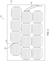
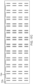
- FIGS. 1 and 2 illustrate conventional structures for solar cell panels 10, which include a substrate 12, a plurality of solar cells 14 arranged in an array, and electrical connectors 16 between the solar cells 14.
- Half size solar cells 14 are shown in FIG. 1 and full size solar cells 14 are shown in FIG. 2 .
- Space solar cells 14 are derived from a round Germanium (Ge) substrate starting material, which is later fabricated into semi-rectangular shapes to improve dense packing onto a solar panel 10. This wafer is often diced into one or two solar cells 14 herein described as half size or full size solar cells 14.
- the electrical connectors 16 providing electrical connections between solar cells 14 are made along the long parallel edge between solar cells 14. These series connections (cell-to-cell) are completed off-substrate, as strings of connected solar cells 14 are built having lengths of any number of solar cells 14. The completed strings of solar cells 14 are then applied and attached to the substrate 12.
- wiring 18 is attached at the end of a string of solar cells 14 to electrically connect the string to other strings, or to terminate the resulting circuit and bring the current off of the array of solar cells 14.
- String-to-string and circuit termination connections are typically done on the substrate 12, and typically using wiring 18.
- some solar cell panels 10 use a printed circuit board (PCB)-type material with embedded conductors.
- PCB printed circuit board
- Adjacent strings of connected solar cells 14 can run parallel or anti-parallel.
- strings of connected solar cells 14 can be aligned or misaligned. There are many competing influences to the solar cell 14 layout resulting in regions where solar cells 14 are parallel or anti-parallel, aligned or misaligned.
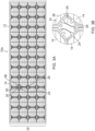
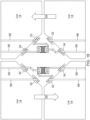
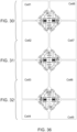
- FIGS. 3A-3B illustrate an improved structure for a solar cell panel 10a, according to one example, wherein FIG. 3B is an enlarged view of the details in the dashed circle in FIG. 3A .
- the various components of the solar cell panel 10a are shown and described in greater detail in FIGS. 5-13 .
- the solar cell panel 10a includes a substrate 12 for solar cells 14 having one or more corner conductors 20 thereon.
- the substrate 12 is a multi-layer substrate 12 comprised of one or more Kapton ® (polyimide) layers separating one or more patterned metal layers.
- Kapton ® polyimide
- the substrate 12 may be mounted on a large rigid panel 10a similar to conventional assembles. Alternatively, the substrate 12 can be mounted to a lighter more sparse frame or panel 10a for mounting or deployment.
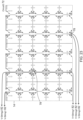
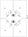
- a plurality of solar cells 14 are attached to the substrate 12 in a two-dimensional (2-D) grid of an array 22.
- the array 22 is comprised of ninety-six (96) solar cells 14 arranged in four (4) rows by twenty-four (24) columns, but it is recognized that any number of solar cells 14 may be used in different implementations.
- the solar cells 14 have cropped corners 24 that define corner regions 26, as indicated by the dashed circle.
- the substrate 12 is configured such that, when corner regions 26 of adjacent ones of the solar cells 14 are aligned, an area 28 of the substrate 12 remains exposed when at least one of the solar cells 14 having at least one cropped corner 24 is attached to the substrate 12.
- the area 28 of the substrate 12 that remains exposed includes one or more of the corner conductors 20, and one or more electrical connections between the solar cells 14 and the corner conductors 20 are made in the corner regions 26 resulting from the cropped corners 24 of the solar cells 14.
- the corner conductors 20 are conductive paths attached to, printed on, buried in, or deposited on the substrate 12, before and/or after the solar cells 14 are attached to the substrate 12, which facilitate connections between adjacent solar cells 14.
- the connections between the solar cells 14 and the corner conductors 20 are made after the solar cells 14 have been attached to the substrate 12.
- four adjacent solar cells 14 are aligned on the substrate 12, such that four cropped corners 24, one from each solar cell 14, are brought together at the corner regions 26.
- the solar cells 14 are then individually attached to the substrate 12, wherein the solar cells are placed on top of the corner conductors 20 to make the electrical connection between the solar cells 14 and the corner conductors 20.
- the solar cells 14 may be applied to the substrate 12 as CIC (cell, interconnect and coverglass) units.
- CIC cell, interconnect and coverglass
- bare solar cells 14 may be assembled on the substrate 12, and then interconnects applied to the solar cells 14, followed by the application of a single solar cell 14 coverglass, multiple solar cell 14 coverglass, multiple solar cell 14 polymer coversheet, or spray encapsulation. This assembly protects the solar cells 14 from damage that would limit performance.
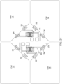
- FIGS. 4A and 4B illustrate an alternative structure for the solar cell panel 10a, according to one example, wherein FIG. 4B is an enlarged view of the details in the dashed circle in FIG. 4A .
- FIG. 4B is an enlarged view of the details in the dashed circle in FIG. 4A .
- PRM power routing module
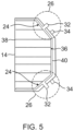
- FIG. 5 illustrates the front side of an exemplary solar cell 14 that may be used in the improved solar cell panel 10a of FIGS. 3A-3B and 4A-4B .
- the solar cell 14, which is a CIC unit, is a half-size solar cell 14. (Full-size solar cells 14 could also be used.)
- the solar cell 14 is fabricated having at least one cropped corner 24 that defines a corner region 26, as indicated by the dashed circle, such that the corner region 26 resulting from the cropped corner 24 includes at least one contact 32, 34 for making an electrical connection to the solar cell 14.
- the solar cell 14 has two cropped corners 24, each of which has both a front contact 32 on the front side of the solar cell 14 and a back contact 34 on a back side of the solar cell 14, where the contacts 32 and 34 extend into the corner region 26.
- Full-size solar cells 14 would have four cropped corners 24, each of which would have a front contact 32 and a back contact 34.
- the cropped corners 24 increase utilization of the round wafer starting materials for the solar cells 14. In conventional panels 10, these cropped corners 24 would result in unused space on the panel 10 after the solar cells 14 are attached to the substrate 12.
- the new approach described in this disclosure utilizes this unused space. Specifically, metal foil interconnects, comprising the corner conductors 20, front contacts 32 and back contacts 34, are moved to the corner regions 26.
- existing CICs have interconnects attached to the solar cell 14 front side, and connect to the back side (where connections occur) during stringing.
- the current generated by the solar cell 14 is collected on the front side of the solar cell 14 by a grid 36 of thin metal fingers 38 and wider metal bus bars 40 that are connected to both of the front contacts 32.
- the bus bar 40 is a low resistance conductor that carries high currents and also provides redundancy should a front contact 32 become disconnected. Optimization generally desires a short bus bar 40 running directly between the front contacts 32. Having the front contact 32 in the cropped corner 24 results in moving the bus bar 40 away from the perimeter of the solar cell 14. This is achieved while simultaneously minimizing the bus bar 40 length and light obscuration. Additionally, the finger 38 length is now shorter. This reduced parasitic resistances in the grid 36 because the length of the fingers 38 is shorter and the total current carried is less. This produces a design preference where the front contacts 32 and connecting bus bar 40 are moved to provide shorter fingers 38.
- FIG. 6 illustrates the back side of the exemplary solar cell 14 of FIG. 5 .
- the back side of the solar cell 14 has a metal back layer 42 that is connected to both of the back contacts 34.
- FIG. 7 illustrates solar cells 14 arranged into the 2D grid of the array 22, according to one example.
- the array 22 comprises a plurality of solar cells 14 attached to a substrate 12, such that corner regions 26 of adjacent ones of the solar cells 14 are aligned, thereby exposing an area 28 of the substrate 12. Electrical connections (not shown) between the solar cells 14 are made in the exposed area 28 of the substrate 12 using the front contacts 32 and back contacts 34 of the solar cells 14 and corner conductors 20 (not shown) formed on or in the exposed area 28 of the substrate 12.
- the solar cells 14 are individually attached to the substrate 12. This assembly can be done directly on a support surface, i.e., the substrate 12, which can be either rigid or flexible. Alternatively, the solar cells 14 could be assembled into the 2D grid of the array 22 on a temporary support surface and then transferred to a final support surface, i.e., the substrate 12.
- FIG. 8 illustrates an example of the array 22 where one or more bypass diodes 44 are added to the exposed area 28 of the substrate 12 in the corner regions 26, for use in one or more of the electrical connections.
- the bypass diodes 44 protect the solar cells 14 when the solar cells 14 become unable to generate current, which could be due to being partially shadowed, which drives the solar cells 14 into reverse bias.
- the bypass diodes 44 are attached to the substrate 12 in the corner regions 26 independent of the solar cells 14.
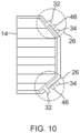
- FIG. 9 illustrates an example where the bypass diode 44 is applied to the back side of the solar cell 14, with interconnects or contacts 46 for the bypass diode 44 connected to the back layer 42 and also extending into the corner region 26 between the front and back contacts 32, 34.
- FIG. 10 illustrates a front side view of the example of FIG. 9 , with the interconnect or contact 46 for the bypass diode 44 (not shown) extending into the corner region 26 between the front and back contacts 32, 34.
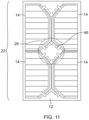
- FIG. 11 illustrates the solar cells 14 of FIGS. 9 and 10 arranged into the 2D grid of the array 22 and applied to the substrate 12, where the bypass diodes 44 (not shown) are applied to the back side of the solar cells 14, with the contacts 46 for the bypass diodes 44 extending into the corner regions 26 of the solar cells 14.
- FIGS. 7 , 8 and 11 are generalized layouts. Specifically, these layouts can be repeated across any panel 10a dimensions desired by a customer. This greatly simplifies assembly, rework, test, and inspection processes.
- Front and back contacts 32, 34 of the solar cells 14 are present in each corner region 26 for attachment to the corner conductors 20.
- Interconnects for the front and back contacts 32, 34 of each of the solar cells 14 are welded, soldered, or otherwise bonded onto the corner conductors 20 to provide a conductive path 20, 32, 34 for routing current out of the solar cells 14.
- Adjacent solar cells 14 can be electrically connected to flow current in up/down or left/right directions as desired by the specific design. Current flow can also be routed around stay-out zones as needed.
- the length or width of the solar cell array 22 can be set as desired. Also, the width can vary over the length of the array 22.
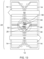
- the electrical connections are series connections that determine a flow of current through the plurality of solar cells 14. This may be accomplished by the connection schemes shown in FIGS. 12 and 13 , wherein FIG. 12 shows up/down series connections 48 between the solar cells 14 of the array 22, and FIG. 13 shows left/right series connections 50 between the solar cells 14 of the array 22.
- these series connections 48, 50 are electrical connections between the front contacts 32 and back contacts 34 of the solar cells 14, and the bypass diodes 44, are made using the corner conductors 20 formed on or in the exposed areas 28 of the substrate 12.
- These series connections 48, 50 determine the current (power) flow, as indicated by the arrows 52, through the solar cells 14, in contrast to the assembly of large strings off-substrate.
- the corner conductors 20 between solar cells 14 can be in many forms. They could be accomplished using wires that have electrical connections made on both ends, which could be from soldering, welding, conducting adhesive, or other process. In addition to wires, metal foil connectors, similar to the interconnects could be applied. Metal conductive paths or traces can also be integrated with the substrate 12.
- this new approach attaches the solar cells 14 individually to a substrate 12 such that the corner regions 26 of one, two, three or four adjacent solar cells 14 are aligned on the substrate 12.
- the solar cells 14 can be laid out so that the cropped corners 24 are aligned and the corner regions 26 are adjacent, thereby exposing an area 28 of the substrate 12.
- Electrical connections between solar cells 14 are made in these corner regions 26 between front contacts 32 and back contacts 34 on the solar cells 14, bypass diodes 44, and corner conductors 20 on or in the exposed area 28 of the substrate 12, wherein these conductive paths are used to create a string of solar cells 14 in a series connection 48, 50 comprising a circuit.
- the substrate 12 could be a PCB, which is rigid, or a flex sheet assembly, which is flexible.
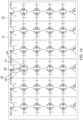
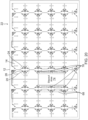
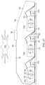
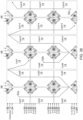
- FIG. 14 illustrates these various components integrated into a larger 2-D grid of an array 22 comprised of five (5) rows by twelve (12) columns of solar cells 14. This array 22 can be expanded as needed using these components.
- the continuous current follows a serpentine path starting from the top left corner, moving down the first column, and then turning to flow up the second column, and then repeating the serpentine path for the following columns to move from left to right, down then up, as indicated by the arrows on the figure.
- the connections for the current are modified to flow in opposite directions, e.g., right to left or left to right, and down then up or up then down, on the figure.
- More electrical connections available in more corner regions 26 simplifies the corner connections and can provide redundancy.
- This disclosure details how a set of corner conductors 20 can be used in fabricating the 2-D grid of the array 22 of solar cells 14.
- This 2-D array 22 can be easily resized to fit the customer's requirements.
- This is a highly structured layout of solar cells 14 and corner conductors 20, which is advantageous for automation of manufacturing, inspection, and testing.
- the corner conductors 20 could be made on any material.
- the corner conductors 20 could be printed directly on the substrate 12, which may comprise a conventional rigid panel, with screen printing or direct write printing (ink jet, aerosol jet, etc.).
- a flex (flexible) substrate 12 such as a flex sheet assembly.
- These substrates 12 are widely available commercially with a history in the space environment.
- a limited area of the substrate 12 could be fabricated comprised of the elements needed in the corner region 26 including the corner conductors 20.
- This limited area of the substrate 12 could be attached to a larger assembly, such as a rigid panel.
- the solar cells 14 could then be applied adjacent to the applied substrates 12 with the corner conductors 20.
- a large area substrate 12 that is a flex sheet assembly could be fabricated that encompasses the area of both solar cells 14 and the corner regions 26..
- This substrate 12 could be fabricated in such a way as to exist on its own. It could be supported by another structure, such as a rigid panel or by elements at the perimeter that support the flex circuit assembly..
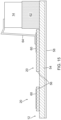
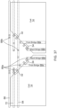
- FIG. 15 shows a side view of a substrate 12 that is flex sheet assembly, according to one example.
- the substrate 12 comprises a polyimide sheet 54 and the corner conductors 20 comprise a patterned Copper (Cu) layer 56 on top of the polyimide sheet 54.
- a conducting back sheet of polyimide 58 can be applied to the polyimide sheet 54, which is useful in a space environment in that it will reduce the accumulation of charge.
- Another capability is the addition of a plated Silver (Ag) or Gold (Au) layer 60 on the Cu layer 56 as part of the corner conductors 20, which is commonly available in a flex sheet assembly. These layers improve the ability to make connections.
- the solar cell 14 Shown on the right side is the solar cell 14 that is attached to the substrate 12 with adhesive 62. Also visible is the metal foil interconnect 64 attached to the solar cell 14 and the plated Ag or Au layer 60 of the corner conductors 20. This is a rather typical construction and assembly that could form the structures presented in earlier figures.
- FIG. 16 illustrates the addition of an insulating polyimide overlay 66 on the substrate 12.
- the polyimide overlay 66 includes holes or apertures that provide access for connections to the Cu layer 56 and/or plated Ag or Au layer 60 of the corner conductors 20.
- the polyimide overlay 66 otherwise encapsulates the flex sheet assembly, including at least portions of the corner conductors 20.
- Polyimide has a high breakdown strength, greater than air or vacuum, and the substrate 12 is covered by the polyimide overlay 66 for preventing ESD, which is an important concern in the space environment. Furthermore, this enables corner conductors 20 to pass under the solar cell 14.
- the adhesive 62 is non-conducting, but the continuous polyimide layer of the polyimide overlay 66 offers significant protection against shorting between buried corner conductors 20 and the solar cell 14.
- FIGS. 17A-17E illustrate the use of buried conductors 68 in the substrate 12, according to different examples.
- FIG. 17A illustrates a buried layer 70 embedded within the substrate 12, configured as shown in FIGS. 3 and 4 , that includes the buried conductors 68 beneath the solar cells 14 that are used for connections between the solar cells 14.
- a dotted outline of a solar cell 14 shows it placement with respect to buried conductors 68.
- a first one of these buried conductors 68 connects both front contacts 32 of the solar cell 14 and a second one of these buried conductors 68 connects both back contacts 34 of the solar cell 14.
- FIG. 17A there are buried conductors 72a across the top of FIG. 17A , which connect between solar cells 14 in adjacent columns of the array 22, where the current path passes between solar cells 14, but not at a cropped corner 24. In an alternative example, this could be accomplished with an extra conductor or wire positioned outside the perimeter of the array 22.
- This configuration also provides for corner-to-corner and column-to-column connections for the plurality of solar cells 14.
- the conductors 68 provide corner-to-corner connections for the plurality of solar cells 14, while the conductors 72a provide column-to-column connections for the plurality of solar cells 14
- FIGS. 17B-17E illustrate various configurations for buried conductors 72b, which are output lines used for circuit termination.
- FIG. 17B illustrates a configuration with one circuit on the substrate 12 with conductors 72b on both ends
- FIG. 17C illustrates a configuration with one circuit on the substrate 12 with conductors 72b coming to the same side (which requires the conductors 72b to extend outside the other conductors 68, 72a)
- FIG. 17D illustrates a configuration where the conductors 72b terminate multiple circuits on the substrate 12 and bring the current out to the edge of the substrate 12 (which can be accomplished with a single Cu layer 56a and an insulating overlay 66)
- FIG. 17E illustrates a configuration showing circuit termination by the conductors 72b for solar cells 14 at the top, middle, and bottom of a column.
- FIG. 18 provides greater detail of the buried conductors 68, which are shown as dashed lines to indicate that they are hidden underneath the solar cells 14.. These buried conductors 68 connect the front contacts 32 or the back contacts 34 of each solar cell 14, which provides significant value.
- the addition of the buried conductors 68 provides redundancy, so that if one interconnect fails, the current flow 52 is maintained. This redundancy is of great importance in a space environment.
- the buried conductors 68 also reduce series resistance. As shown in FIG. 5 , the current from the solar cell 14 is collected on the front side of the solar cell 14 by thin metal fingers 38 and bus bar 40 that stretch across the front of the solar cell 14. There is a balance between the addition of metal for the bus bar 40, which reduces the light entering the solar cell 14 and its output power, and the reduced resistance and redundancy of having more metal for the bus bar 40.
- the addition of the buried conductors 68 in FIG. 18 allows the use of less metal in the bus bar 40, which increases power.
- a similar structure could be used for the configuration at the top and/or bottom of each column of solar cells 14 in the array 22, as current passes between the solar cells 14.
- an additional buried conductor 72a as shown in FIG. 17A could extend horizontally, e.g., left to right, bridging solar cells 14 in adjacent columns of the array 22.
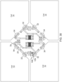
- FIG. 19 shows an example where there is a missing or omitted solar cell 14 in the bottom left portion labeled as a stayout area 74.
- Many panels 10a will have stayout areas 74 dedicated to the mechanical assembly of the panel 10a, wing, satellite or for other reasons dictated by the customer, and these stayout areas 74 cannot include solar cells 14. However, these stay-out areas 74 complicate the assembly of the solar cells 14 greatly.
- the buried conductors 68 shown provide for an ability to accommodate the stay-out area 74 where there is no solar cell 14.
- the current continues to flow through the buried conductors 68 bypassing the stay-out area 74 as indicated by arrow 52.
- the bypass diode 44 is replaced with a conductor 76. This combination allows the current flow 52 to continue redundantly using both conductors 68 in the absence of a solar cell 14 in the stay-out area 74.
- FIG. 20 shows the 2-D array 22 having a large stay-out area 74 in place of four omitted solar cells 14. Also shown are the conductors 76 replacing four bypass diodes 44.
- the design can be modified to accommodate the customization needs of the customer.
- This section addresses these problems by selecting current pathways for the solar cells 14 by adding conductive elements to a corner region 26 to bridge between conductive paths, or by removing conductive elements from a corner region 26 to isolate between conductive paths.
- the corner region 26 is otherwise wasted on the panel 10a, but now is utilized to aid in the panel 10a manufacturing.
- it is possible to select current pathways to direct current or power to a next solar cell 14 in a circuit or to terminate the string.
- current pathways can have two routes.
- One route is a series connection 48, 50 of solar cells 14, while another route is circuit termination.
- a simple step such as adding a conductive element or removing a conductive element, is used to select a current pathway and route. This enables a simple, uniform design and layout, while also achieving the ability to easily adjust the circuit length as needed.
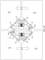
- FIG. 21 further illustrates a generic layout between a plurality of solar cells 14, according to one example.
- the connection scheme has not been determined yet, and each side could be either series or circuit termination.
- the generic layout includes electrical connections between the front contacts 32 and back contacts 34 of the solar cells 14, and the bypass diodes 44, made in the exposed areas 28 of the substrate 12, using the corner conductors 20.
- FIG. 22 illustrates an example where one or more conductor elements comprising a jumper 78 is added to the corner region 26 to select current pathways for the solar cells 14, wherein the jumper 78 bridges the electrical connections from at least one of the corner conductors 20 to one or more other conductive paths.
- the jumper 78 is welded or soldered between a corner conductor 20 and a pad 80, and may include stress relieving elements.
- the pad 80 terminates the circuit to a wire 82, wherein the wire 82 is connected to circuitry external to the solar cells 14.
- the jumper 78 may also channel current to another solar cell 14.
- the jumper 78 is a metal foil interconnect that is similar to existing metal interconnects used in solar cell panels 10.
- the jumper 78 has a shape comprised of two flange elements with parallel planes connected by a web element, which enables multiple connection points, although other shapes may be used as well.
- the solar cell 14 on the bottom right hand side has the jumper 78 moved slightly to the side, which connects the back contact 34 of the bottom, right solar cell 14 to the pad 80. Also shown is the bottom wire 82 attached to the pad 80, wherein the bottom wire 82 connects the string to external circuitry.
- the back contact 34 termination is a V+ terminal.
- the top right solar cell 14 has a top wire 82 applied to another pad 80, which forms a V- terminal.
- the top wire 82 connected to the V- terminal connects to the front contact 32 for standard operation and through the bypass diode 44 to the back contact 34.
- the jumper 78 may be applied to enable termination of a string of solar cells 14, wherein wires 82 are connected to two solar cells 14 via pads 80.
- the jumper 78 may also be applied at a top of a row of solar cells 14 in the array 22 to enable continuation of a string of solar cells 14.
- the jumper 78 may be applied at a top of a row of solar cells 14 in the array 22 to enable termination of a string of solar cells 14, wherein wires 82 are connected to the two solar cells 14 via pads 80.
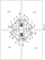
- FIG. 23 shows the combination of these structures into a 2-D grid of an array 22, wherein the solar cells 14 are half-size solar cells 14.
- Jumper 78 positions are adjusted in order to have series connections 48, 50 or string terminations.
- the top left-most solar cell 14 starts a new circuit with a terminal wire 82 labeled V- String 1.
- Solar cells 14 are series connected until the fourth column of solar cells 14 from left to right.
- the jumpers 78 terminate the wire 82 labeled V+ String 1 and start with the wire 82 labeled V- String 2 on the next solar cell 14. This continues until the bottom of the 7th and 8th columns of solar cells 14, where the next circuits are terminated, at the wire 82 labeled V+ String 2 and the wire 82 labeled V- String 3.
- the conductor 72 labeled as String 3 continues the circuit to later columns of solar cells that are not drawn.
- this structure is significant. Now, there is a single printed corner conductor 20 pattern, single layout of solar cells 14, and single layout of bypass diodes 44. This single configuration enables automation of manufacturing, testing, and inspection. The application of a jumper 78 provides for a simple way to control the number of solar cells 14 in a string.
- an electrical connection is made to enable choice of a current path. This is done by adding or removing conducting elements to select current pathways for the solar cells 14.
- the patterned corner conductors 20 could be fabricated, such that there is solid metal where the jumpers 78 are shown in the figures.
- the connection could be accomplished by printed metal, which could involve a variety of metal powder configurations held together with polymer, epoxy, adhesive matrices or that solidify into a solid metal matrix. The removal of metal from one of the current paths would accomplish the same final result, for example, using laser ablation equipment to perform this task.
- This section describes the incorporation of multilayer conductors embedded in the substrate 12 for electrically connecting to the corner conductors 20 and the solar cells 14.
- the multilayer conductors pass underneath, and parallel or orthogonal to, the corner conductors 20 and the solar cells 14.
- These multilayer conductors also carry power from any point on the 2-D grid of the array 22 of solar cells 14 to a perimeter of the substrate 12, without the need for external wiring 82, which simplifies the extraction of power from the circuits in the array 22.
- FIG. 24 illustrates another configuration for the buried metal layer 70 embedded within the substrate 12, configured as shown in FIGS. 3 and 4 .
- the buried metal layer 70 includes the conductors 68, 72 beneath the solar cells 14, which are bridge lines for electrically connecting between cropped corners 24 of the solar cells 14, wherein the buried conductors 68, 72 are configured in the same manner as shown in FIG. 17 .
- the buried metal layer 70 also include V+ lines 84 and V- lines 86 for distributing power among the solar cells 14, wherein the V+ lines 84 and V- lines 86 are configured horizontally in the buried metal layer 70 of the substrate 12, orthogonal to the conductors 68, passing underneath the solar cells 14 to the perimeter of the substrate 12.
- the conductors 68 as bridge lines can be configured in a number of different ways: the conductor 68 runs under the solar cells 14 to electrically connect a front contact 32 on one corner 24 of the solar cell 14 to a front contact 32 on another corner 24 of the same solar cell 14; the conductor 68 runs under the solar cell 14 to electrically connect a back contact 34 on one corner 24 of the solar cell 14 to a back contact 34 on another corner 24 of the same solar cell 14.
- the string termination lines V+ 84 and V- 86 can be configured in a number of different ways: the V+ lines 84 and V- lines 86 distribute current from the solar cells 14 to a perimeter of the substrate 12; the V+ line 84 and V-line 86 run at least a portion of a length of the array 22 in a perpendicular direction to the array 22; or there are a plurality of the V+ lines 84 and V- lines 86, and the solar cells 14 connect to the plurality of the V+ lines 84 and V- lines 86 for distributing power among the solar cells 14.
- each corner region 26 there may be one or more vias or vertical conduction paths (not shown) through the substrate 12 that vertically connect the conductors 68, 72, the V+ line 84 and the V- line 86 to the solar cells 14 and corner conductors 20.
- the conductors 68, 72, the V+ line 84 and the V- line 86 may be vertically connected to other conductors 68, 72, V+ line 84 and V- line 86, respectively.
- FIG. 25 shows a side view of an example wherein the substrate 12 is a flex sheet assembly including multilayer conductors.
- the substrate 12 includes a polyimide base layer 54 with Cu layer 56a above and Cu layer 56b below, wherein Cu layers 56a and 56b form a multilayer conductor.
- Cu layer 56a with plated Ag or Au layer 60 is patterned as the corner conductors 20 for one layer to the multilayer conductors, and Cu layer 56b is patterned as the conductors 68 and 72, as well as the V+ line 84 and V- line 86, for another layer to the multilayer conductors.
- the substrate 12 also includes insulating layers that separate at least one of the multilayer conductors from at least another one of the multilayer conductors.
- insulating layers that separate at least one of the multilayer conductors from at least another one of the multilayer conductors.
- a conducting polyimide layer 58 can be applied to the back surface of the substrate 12.
- the top polyimide overlay layer 66a can be omitted underneath the solar cell 14. This can be advantageous if the top polyimide overlay layer 66a is prone to bubbles or other defects.
- top polyimide overlay layer 66a There is an alignment between Cu layer 56a, Cu layer 56b and the top polyimide overlay layer 66a.
- the top polyimide overlay layer 66a almost fully encases the Cu layer 56a, polyimide layer 54, and Cu layer 56b, with only small access holes to the Cu layer 56a and Cu layer 56b. This requires the top polyimide overlay layer 66a to roll up and over the corners of the Cu layers 56a and 56b.
- the top polyimide overlay layer 66a provides valuable protection against ESD.
- the top polyimide overlay layer 66a has larger holes to avoid overlapping the edges of the Cu layers 56a and 56b. This top polyimide overlay layer 66a may be easier to fabricate with less defects than a full top polyimide overlay layer 66a.
- top polyimide overlay layer 66a may not be needed; in that case, there would be no hindrance of the top polyimide overlay layer 66a to any jumper 78 connection.
- a jumper 78 (not shown) can connect directly from the Cu layer 56a to the Cu layer 56b.
- the interconnect 64 may connect the solar cell 14 to either Cu layer 56a or Cu layer 56b. This eliminates the Cu-plated via 88 connections, which could be a reliability concern, especially in the flex sheet assembly.
- the thickness of the top polyimide overlay layer 66a is typically about ⁇ 0.1 mm, while the length of the jumper typically may be about ⁇ 4 mm. Having the metal of the jumper 78 surrounded by large amounts of polyimide from the top polyimide overlay layer 66a may impede the jumper 78, but will also impede ESD, which can be valuable.
- the traces of the Cu layer 56b that comprise the V+ line 84 and V- line 86 can be wide to maximize the Cu cross-sectional area and conductivity. This can be important for high currents and long conductors. These V+ line 84 and V- line 86 can have multiple vias 88 that connect to them, making for redundant reliable connections, as shown in FIG. 26 below. Alternatively, these V+ line 84 and V- line 86 can thin, so that there more of them. More lines 84, 86 may be important for arrays 22 with many circuits needing individual output lines 84, 86.
- FIG. 26 shows the corner-to-corner bridge lines 68a, 68b, as well as the V+ line 84 and V- line 86, which are in the Cu layer 56b and are connected by vias 88. While the bridge lines 68a, 68b could be in the Cu layer 56a with a top polyimide overlay 66a, the Cu layer 56b can be thinner or thicker than the Cu layer 56a, as needed. Another option is that these bridge lines 68a, 68b could exist in both Cu layer 56a and Cu layer 56b, providing bottom resistance and improved redundancy. This figure focuses on buried conductors, and a final structure will also have corner conductors 20.
- FIG. 27 shows a standard connection between three solar cells 14a, 14b, 14c arranged on a substrate 12 and connected in a series using corner conductors 20 with bypass diodes 44a, 44b, 44c.
- Each solar cell 14a, 14b, 14c is depicted as a diode 90 in parallel with a current source 92 in parallel with a shunt resistor 94.
- the current 52 flows clockwise around the figure. As current 52 returns from a load 96 at a low voltage (V-) 98, it connects to the front contact 32 of solar cell 14a and to bypass diode 44a. If solar cell 14a is illuminated by light source 100, the current source 92 operates and boosts the voltage 98 of the current 52 through the solar cell 14a.
- This series of solar cells 14a, 14b, 14c is known as a string, producing a desired current 52 and voltage 98.
- the number of solar cells 14a, 14b, 14c in the circuit determines the voltage 98, which is roughly 2V per triple junction solar cell 14a, 14b, 14c.
- a solar cell 14a, 14b, 14c does not produce current 52, due to shadowing, for example, the voltage 98 of the circuit will be applied across the shadowed solar cell 14a, 14b, 14c and likely damage it.
- the bypass diode 44a, 44b, 44c protects against this. If solar cell 14b is not producing current 52, then voltage 98 will develop across the solar cell 14b and bypass diode 44b, which will enable current 52 to flow through bypass diode 44b.
- Use of a Silicon (Si) bypass diode 44b will enable current 52 flow at roughly 0.5V, protecting the solar cell 14b.
- the connections described here need to be maintained in the configurations described in further figures. Furthermore, redundancy of conductors and connections is important to ensure operation over the lifetime of the solar cells 14a, 14b, 14c.
- FIG. 28 shows how the buried Cu layer 56b integrates with the Cu layer 56a, which comprise the corner conductors 20.
- Vias 88a are shown for connections between Cu layer 56a, which are corner conductors 20, and Cu layer 56b, which are bridge lines 68.
- Vias 88b are also shown for connections between Cu layer 56a, which are power distribution bars 102, and Cu layer 56b, which are V+ line 84 and V- line 86. Interconnects can connect these bars 102 to multiple solar cells 14 and to multiple V+ lines 84 and V- lines 86.
- Bypass diodes 44 are also shown.
- FIG. 29 shows a jumper 78a that connects the back contact 34 of the top left solar cell 14 to the front contact 32 of the bottom left solar cell 14.
- This jumper 78a also connects through the bypass diode 44 to the back contact 34 of the bottom left solar cell 14.
- This connection path provides for the current flow 52 from top to bottom shown on the left side of the figure.
- a similar configuration using jumper 78b provides for the current flow 52 from bottom to top shown on the right side of the figure.
- FIGS. 30 , 31 , 32 , 33 , 34 and 35 illustrate some of the advantages of this disclosure.
- the single design of the flex sheet assembly can have many electrical connection pathways. This is important for bottoming the cost to purchase material and simplifies the manufacturing and automation.
- FIG. 30 shows a connection between the solar cells 14 on the top left and bottom left of the figure.
- the solar cell 14 on the bottom left terminates the back contact 34 to the center power bars 102, which are connected to the V+ lines 84 (not shown) and V-lines 86 (not shown) through the interconnects 106 to the vias 88b.
- the power distribution bars 102 in the center have a bridging interconnect 104 allowing access to all of the V+ lines 84 and V- lines 86 through the interconnects 106 to the vias 88b.
- the solar cell 14 on the bottom right of the figure terminates the front contact 32 to the right side power bar 102, which is connected to the V- line 86 through the interconnects 106 to the vias 88b, and the back contact 34 is series connected to the solar cell 14 on the top right of the figure.
- the arrows 52 indicate the direction of current flow.
- FIG. 31 shows the back contact 34 of the solar cell 14 on the top left of the figure terminated to the top center power bar 102, which is connected to the V+ lines 84 (not shown) and V- lines 86 (not shown) through the interconnects 106 to the vias 88b, while the solar cell 14 on the bottom left of the figure terminates the front contact 32 to the left side power bar 102, which is connected to the V- line 86 through the interconnect 106 to the vias 88b.
- the back contact 34 of the solar cell 14 on the bottom right of the figure is terminated to the bottom center power bar 102, which is connected to the V+ lines 84 and V- lines 86 through the interconnects 106 to the vias 88b, while the solar cell 14 on the top left of the figure terminates the front contact 32 to the right side power bar 102, which is connected to the V- line 86 through the interconnect 106 to the vias 88b.
- FIG. 32 shows the front contact 32 of the solar cell 14 on the top left of the figure connected to the left side power distribution bar 102, which is connected to the V- line 86 (not shown) through the interconnects 106 to the vias 88b, with the back contact 34 series connected to the solar cell 14 on the bottom left of the figure.
- the back contact 34 of the solar cell 14 on the bottom right of the figure is connected to the solar cell 14 on the top right of the figure, while the back contact 34 of the solar cell 14 on the top right of the figure is terminated to the top center power distribution bar 102, which is connected to the V+ line 84 (not shown) through the interconnects 106 to the vias 88b.
- FIG. 33 shows the back contact 34 of the solar cell 14 on the top left of the figure is terminated to the top center power distribution bar 102, which is connected to the V+ line 84 line (not shown) through the interconnects 106 to the vias 88b, while the front contact 32 of the solar cell 14 on the top left of the figure is connected to the bridge line 68 (not shown) through the via 88a.
- the front contact 32 of the solar cell 14 on the bottom left of the figure is connected to the left side power distribution bar 102, which is connected to the V- line 86 (not shown) through the interconnect 106 to the vias 88b, as well as the bypass diode 44, while the back contact 34 of the solar cell 14 on the bottom left of the figure is also connected to the V- line 86 through the bypass diode 44.
- the back contact 34 of the solar cell 14 on the bottom right of the figure is series connected to the solar cell 14 on the top right of the figure.
- FIG. 34 shows the back contact 34 of the solar cell 14 on the top left of the figure is series connected to the solar cell 14 on the bottom left of the figure.
- the back contact 34 of the solar cell 14 on the bottom left of the figure is connected to the bottom center power distribution bar 102, which is connected by the interconnect 104 to the top center power distribution bar 102, which is terminated to the V+ line 84 (not shown) through the interconnects 106 to the vias 88b.
- the back contact 34 of the solar cell 14 on the bottom right of the figure is series connected to the solar cell 14 on the top right of the figure.
- FIG. 35 shows the front contact 32 of the solar cell 14 on the top left of the figure connected to the left side power distribution bar 102, which is connected to the V- 84 (not shown) through the interconnect 106 to the vias 88b, while the back contact 34 of the solar cell 14 on the top left of the figure is series connected to the solar cell 14 on the bottom left of the figure.
- the back contact 34 of the solar cell 14 on the bottom right of the figure is series connected to the solar cell 14 on the top right of the figure.
- FIG. 36 The description of FIG. 36 is made with reference to FIGS. 30 , 31 and 32 appended together.
- the solar cells 14 of FIGS. 30 , 31 and 32 are connected such that the current in the left side travels down the solar cells 14, which are series connected, terminated to the V+ line 84 and/or terminated to the V- line 86.
- the solar cells 14 of FIGS. 30 , 31 and 32 are connected such that the current in the right side travels up the solar cells 14, which are series connected, terminated to the V+ lines 84 and/or terminated to the V- lines 86.
- the cells of FIGS. 33 , 34 and 35 may be appended together in a similar but mirrored manner, with the current flow reversed.
- FIG. 37 shows the conductors 72, V+ lines 84 and V- lines 86 at the end of a column of solar cells 14, as well as the bridge lines 68a, 68b under the solar cells 14.
- an interconnect (not shown) may be applied for series connection.
- the solar cell 14 on the left side of the figure can be terminated to the V- line 86 through via 88b.
- the solar cell 14 on the right side of the figure can be terminated to the V+ line 84 through the via 88b.
- FIG. 38 shows a variation comprising an array 22 of solar cells 14 arranged as three (3) rows by six (6) columns.
- the figure indicates the bridges 68 and 72, as well as multiple V+ lines 84 and V- lines 86.
- the solar cell 14 in the top left corner (cell1 14) terminates on the V- 1,2,3 lines 86 using both corners for these connections.
- the current of the first circuit then flows through series connections to cell7 14, as indicated by the arrow 52a, wherein cell7 14 terminates onto V+ 1,2,3 lines 84.
- the current of the second circuit then starts with cell8 14 terminating on V- 3,5 lines 86, as indicated by the arrow 52b, wherein the circuit is series connected between cell8 14 and cell 15 14 and cell15 14 terminates on V+ 6,7,10 lines 84.
- the current of the third circuit starts with cell 16 14 connected to V- 5,6 lines 86, as indicated by the arrow 52c, and the circuit then continues with series connection through cell 18 14 and off the figure.
- This configuration shows the advantages of this disclosure.
- the strength of this disclosure is that a single design of this expensive part is needed.
- the expense can be reduced by fabricating in bulk.
- the long delivery time is eliminated as it becomes an off-the-shelf item that can be fabricated in advance for any variety of programs, customers, etc.
- Having such a structured layout also simplifies the layout automation, and as well as testing and inspection.
- the procurement of a multilayer substrate 12 and its assembly with solar cells 14 and bypass diodes 44 is generic. This is an assembly common for any rectangular solar cell array 22.
- Solar cell arrays 22 have different operating environments and voltage requirements which ultimately determine the number of solar cells 14 in a circuit.
- the string length often ranges from 20 to 55 solar cells 14. This is a critical customization.
- the addition of the conducting interconnect is equivalent to having these traces fabricated in place and then having the metal removed.
- the removal could easily be accomplished through a laser ablation process.
- a base level layout could be where all connections are made as the starting point. Then, metal could be removed, in order to have a desired connection pattern. Moreover, there may be electrical paths through the Cu layers via a plated via, or the removal of at least portions of the Cu layers. Some of the polyimide may also be removed in this process.
- Panel 10a fabrication often involves customer direction to not have any hardware in a certain location that may have a hole or serve other mounting needs of the panel 10a assembly.
- the corner-to-corner buried connections enable solar cells 14 to be left off of the assembly. Then, the bypass diode 44 is replaced with a solid conductor. This may result in severing V+ lines 84 or V- lines 86, which would need to remain unused.
- the center power distribution bar 102 can be solid, which provides access to more V+ lines 84.
- only one solar cell 14 could terminate on the V+ line 84 in a corner region 26.
- the structure has more hard wired connections and thus less choices and less interconnects.
- Hard wired electrical connections reduce failure risk, which is often desirable.
- V+ lines 84 and V- lines 86 This is balanced against a solar cell 14 being able to terminate to V+ lines 84 and V- lines 86 in both corner regions 26, which provides redundancy and design flexibility in case some V+ lines 84 and V- lines 86 are already in use. Also, this requires use of V+ lines 84 and V- lines 86 that are adjacent, eliminating the protection of using V+ lines 84 and V- lines 86 in different corner regions 26.
- FIG. 39 shows the connections made to match those of FIG. 33 , but with fewer corner conductors 20, jumpers 78, interconnects 104 and interconnects 106. Furthermore, there is more space between the corner conductors 20 and other conductive elements.
- corner conductors 20 can be more widely spaced for better ESD protection or to shrink the required corner region 26.
- a small corner region 26 results in more solar array area used to produce power.
- This section describes printing metal corner conductors 20 on the substrate 12 in the corner regions 26, before and/or after the solar cells 14 and/or diodes 44 are attached to the substrate 12, to provide the electrical connections between solar cells 14.
- the printing of corner conductors 20 can simplify manufacturing, while providing for customization.
- the electrical connections can be made in any desirable way using the printed corner conductors 20, with little effort to modify the design.
- FIG. 40 shows a corner connection layout similar to FIG. 22 discussed above. This figure illustrates how one or more conductor elements, such as a jumper 78, are added to the corner regions 26.
- the jumper 78 allows circuits to be terminated at the corner region 26 or to channel current 52 to the next solar cell 14.
- the jumper 78 is a metal foil element that is similar to existing metal interconnects. As described above, the jumper 78 has a shape comprised of two flange elements, which have parallel planes, connected by a web element, which enables multiple connection points, although other shapes may be used as well.
- the jumper 78 could be welded or soldered onto conducting paths and pads. Other types of conductor elements, such as wires 82, could also be employed.
- the jumper 78 allows selection between two possible current pathways.
- the layout of FIG. 40 provides a pathway of series connection of the solar cell 14 or circuit termination to the large pad 80 where a wire 82 could be attached.
- FIG. 41 shows how the jumper 78 could be replaced with a printed conductor 108 of similar shape.
- the printed conductor 108 may also require curing, but does not require a weld or solder process, which could be advantageous.
- FIG. 42 the corner regions 26 are shown having corner conductors 20 that are printed on the exposed area 28 of the substrate 12 before the solar cells 14 and bypass diodes 44 are applied to the substrate 12.
- the printing of the corner conductors 20 can connect these elements in virtually any manner or configuration.
- the primary constraint is to avoid crossing corner conductors 20.
- the layout of FIG. 42 is generic, and could be built in bulk and applied to any panel 10a configuration, which is an advantage for manufacturing cost and delivery times.
- FIGS. 43A and 43B the corner regions 26 are shown having corner conductors 20 that are printed on the exposed area 28 of the substrate 12. This printing could happen before or after solar cells 14 and bypass diodes 44 are attached. It is preferred to do this printing before the solar cells 14 and bypass diodes 44 are attached to facilitate curing or cleanup that may be needed.
- These figures show how printing the corner conductors 20 can direct the flow of current, as indicated by the arrows 52. The printing technique allows for customization, where FIG. 43A has the current 52 flowing vertically, while FIG. 43B has the current 52 flowing horizontally.
- FIG. 44 shows another configuration of printed corner conductors 20 where the circuits terminate at large pads 80, which are also printed, and to which a bulk wire 82 can be connected (not shown).
- the printing of corner conductors 20 and pads 80 can be extended to any number of different layouts and configurations to achieve left-right or top-bottom current paths, stayout zones, etc.
- the addition of buried or multilayer connections embedded in the substrate 12 can also be connected with the printed corner conductors 20 and pads 80, which can conform over the topographies.
- the printed conductors 20 could connect to vias at the surface to buried conductors. Similarly, a buried conductor may be exposed through an insulation layer. The printing can be made across the substrate 12 surface and extend down to the exposed, buried conductor.
- the corner conductors 20 are printed directly on the substrate 12, in order to simplify manufacturing, while enhancing customization.
- the printed corner conductors 20 can be designed for any configuration. Printed corner conductors 20 may require curing, but do not require welding or soldering processes. Instead, the printed corner conductors 20 directly connect the solar cells 14, via their front contacts 32 and back contacts 34, with other elements, such as bypass diodes 44.
- the printed corner conductors 20 need to be highly conductive, have ultra-low outgassing, and cure with a maximum temperature below 250°C.
- Some printable conductors include significant polymer content that may not satisfy these requirements.
- formulations based on nano-metal inks that are preferable, including nano-metal inks available in Au, Ag and Cu.
- Plasma spray of micro-metal particles has also shown the ability to print a polymer-free metal with high conductivity.
- nano-metal inks are comprised of powders that solidify into a solid metal in the temperature range of about 150-250°C. During curing, solvent and surfactants largely evaporate, leaving little polymer or organic content. The resulting metal corner conductors 20 have a conductivity near that of bulk metal. Furthermore, a variety of printing tools are available to print these nano-metals in ink form or as an aerosol process.
- the functionality of the printed corner conductors 20 is enhanced by the use of buried or multilayer conductors embedded in the substrate 12.
- the printed corner conductors 20 can be encapsulated in polymer insulators, which also can be printed, to reduce sensitivity to ESD.
- the printing of corner conductors 20 and pads 80 can also involve the printing of an insulator, which is a polymer or ceramic/oxide.
- the insulator is printed on the corner conductors 20 and pads 80, in order to encapsulate the printed corner conductors 20 and pads 80, and reduce sensitivity to ESD.
- another printed conductive layer could be deposited on the insulator to carry radiation-induced charges.
- this structure is significant. Now, there is a single printed corner conductor 20 pattern, single layout of solar cells 14, and single layout of bypass diodes 44. This single configuration has great advantages for automation of manufacturing, testing, and inspection.
- Printing of conducting pathways is an advantageous process to achieve the needed customization.
- a wide variety of pathways can be achieved using a single starting layout of FIG. 42 , where only needed current pathways exist. This allows the corner regions 26 to be more fully utilized. Tradeoffs and optimization can be changed. Since fewer corner conductors 20 are needed in the corner regions 26, the corner regions 26 can be shrunk, increasing the fraction of panel 10a area with power-producing solar cells 14. Alternatively, corner conductors 20 can be larger to reduce resistance and gain reliability. In another tradeoff, larger spaces between corner conductors 20 can be designed, which results in less risk of damage from ESD. These characteristics are of great value in a space-based panel 10a.
- Examples of the disclosure may be described in the context of a method 114 of fabricating a solar cell 14, solar cell panel 10a and/or satellite, comprising steps 116-128, as shown in FIG. 45 , wherein the resulting satellite 130 having a solar cell panel 10a comprised of solar cells 14 are shown in FIG. 46 .
- exemplary method 114 may include specification and design 116 of the solar cell 14, solar cell panel 10a and/or satellite 130, and material procurement 118 for same.
- component and subassembly manufacturing 120 and system integration 122 of the solar cell 14, solar cell panel 10a and/or satellite 130 takes place, which include fabricating the solar cell 14, solar cell panel 10a and/or satellite 130.
- the solar cell 14, solar cell panel 10a and/or satellite 130 may go through certification and delivery 124 in order to be placed in service 126.
- the solar cell 14, solar cell panel 10a and/or satellite 130 may also be scheduled for maintenance and service 128 (which includes modification, reconfiguration, refurbishment, and so on), before being launched.
- a system integrator may include without limitation any number of solar cell, solar cell panel, satellite or spacecraft manufacturers and major-system subcontractors;
- a third party may include without limitation any number of venders, subcontractors, and suppliers; and
- an operator may be a satellite company, military entity, service organization, and so on.
- a satellite 130 fabricated by exemplary method 114 may include systems 132, a body 134, solar cell panels 10a comprised of solar cells 14, and one or more antennae 136.
- the systems 132 included with the satellite 130 include, but are not limited to, one or more of a propulsion system 138, an electrical system 140, a communications system 142, and a power system 144. Any number of other systems 132 also may be included.
- FIG. 47 is an illustration of the solar cell panel 10a in the form of a functional block diagram, according to one example.
- the solar cell panel 10a is comprised of the solar cell array 22, which is comprised of one or more of the solar cells 14 individually attached to the substrate 12.
- Each of the solar cells 14 absorbs light 146 from a light source 148 and generates an electrical output 150 in response thereto.
- At least one of the solar cells 14 has at least one cropped corner 24 that defines a corner region 26, such that an area 28 of the substrate 12 remains exposed when the solar cell 14 is attached to the substrate 12.
- the corner regions 26 of adjacent ones of the solar cells 14 are aligned, thereby exposing the area 28 of the substrate 12.
- the area 28 of the substrate 12 that remains exposed includes one or more corner conductors 20 attached to, printed on, or integrated with the substrate 12, and one or more electrical connections between the solar cells 14 and the corner conductors 20 are made in a corner region 26 resulting from the cropped corner 24 of the at least one of the solar cells 14.
- the corner region 26 resulting from the cropped corner 24 includes at least one contact, for example, a front contact 32 on a front side of the solar cell 14 and/or a back contact 34 on a back side of the solar cell 14, for making the electrical connections between the corner conductors 20 and the solar cell 14.
- the electrical connections may comprise up/down or left/right series connections that determine a flow of power through the solar cells 14, and may include one or more bypass diodes 44.
Landscapes
- Photovoltaic Devices (AREA)
Claims (15)
- Substrat (12) pour des cellules solaires (14), le substrat (12) étant configuré de telle manière que :une zone (28) du substrat (12) reste à découvert lorsqu'au moins une cellule solaire (14), pourvue d'au moins un coin tronqué (24) qui définit une région en coin (26), est fixée au substrat (12) ;caractérisé en ce quela zone (28) du substrat (12) qui reste à découvert comporte un ou plusieurs conducteurs en coin (20) formant des chemins conducteurs fixés à, imprimés sur, noyés dans, ou déposés sur le substrat (12) ; etdes connexions électriques entre l'au moins une cellule solaire (14) et les un ou plusieurs conducteurs en coin (20) sont réalisées dans la région en coin (26).
- Substrat selon la revendication 1, dans lequel les conducteurs en coin (20) sont recouverts d'une couche isolante (66).
- Substrat selon l'une quelconque des revendications 1 à 2, dans lequel l'au moins une cellule solaire (14) est appelée à être placée au-dessus des conducteurs en coin (20).
- Substrat selon l'une quelconque des revendications 1 à 3, dans lequel les conducteurs en coin (20) passent sous l'au moins une cellule solaire (14) lorsqu'elle est fixée.
- Substrat selon l'une quelconque des revendications 1 à 4, dans lequel les conducteurs en coin (20) s'inscrivent en dehors d'un périmètre de l'au moins une cellule solaire (14) lorsqu'elle est fixée.
- Substrat selon l'une quelconque des revendications 1 à 5, dans lequel les conducteurs en coin (20) passent d'un coin tronqué (24) à un autre coin tronqué (24) de l'au moins une cellule solaire (14) lorsqu'elle est fixée.
- Substrat selon l'une quelconque des revendications 1 à 6, dans lequel l'au moins une cellule solaire (14) comprend une pluralité de cellules solaires (14) qui sont appelées à être fixées au substrat (12) dans une grille bidimensionnelle d'un réseau (22).
- Substrat selon la revendication 7, dans lequel les connexions électriques sont des connexions en série qui établissent une circulation de courant à travers la pluralité de cellules solaires (14) lorsqu'elles sont fixées.
- Substrat selon la revendication 7 ou 8, dans lequel les connexions électriques terminent une chaîne de la pluralité de cellules solaires (14) lorsqu'elles sont fixées.
- Substrat selon l'une quelconque des revendications 7 à 9, dans lequel les conducteurs en coin (20) passent d'un coin tronqué (24) de l'une de la pluralité de cellules solaires (14) à un coin tronqué (24) d'une autre de la pluralité de cellules solaires (14).
- Substrat selon l'une quelconque des revendications 1 à 10, dans lequel les conducteurs en coin (20) permettent aux connexions électriques de quitter le substrat (12).
- Substrat selon l'une quelconque des revendications 1 à 11, dans lequel une ou plusieurs diodes bypass (44) sont ajoutées à la zone (28) du substrat (12) qui reste à découvert en vue de leur utilisation dans une ou plusieurs des connexions électriques.
- Panneau (10a) de cellules solaires comprenant un substrat (12) selon l'une quelconque des revendications 1 à 12 et un réseau (22) de cellules solaires (14) fixées au substrat (12).
- Panneau de cellules solaires selon la revendication 13, dans lequel l'au moins une cellule solaire (14) comporte un contact avant (32) sur une face avant de l'au moins une cellule solaire (14), de préférence le contact avant (32) s'étendant jusque dans la région en coin (26).
- Panneau de cellules solaires selon la revendication 13 ou 14, dans lequel l'au moins une cellule solaire (14) comporte un contact arrière (34) sur une face arrière de l'au moins une cellule solaire (14), de préférence le contact arrière (34) s'étendant jusque dans la région en coin (26).
Priority Applications (1)
| Application Number | Priority Date | Filing Date | Title |
|---|---|---|---|
| EP23169034.8A EP4235815A3 (fr) | 2016-09-14 | 2017-09-14 | Conducteurs préfabriqués sur un substrat pour faciliter des connexions d'angle pour un réseau de cellules solaires |
Applications Claiming Priority (19)
| Application Number | Priority Date | Filing Date | Title |
|---|---|---|---|
| US201662394636P | 2016-09-14 | 2016-09-14 | |
| US201662394667P | 2016-09-14 | 2016-09-14 | |
| US201662394629P | 2016-09-14 | 2016-09-14 | |
| US201662394616P | 2016-09-14 | 2016-09-14 | |
| US201662394666P | 2016-09-14 | 2016-09-14 | |
| US201662394649P | 2016-09-14 | 2016-09-14 | |
| US201662394641P | 2016-09-14 | 2016-09-14 | |
| US201662394623P | 2016-09-14 | 2016-09-14 | |
| US201662394632P | 2016-09-14 | 2016-09-14 | |
| US201662394627P | 2016-09-14 | 2016-09-14 | |
| US201662394671P | 2016-09-14 | 2016-09-14 | |
| US201662394672P | 2016-09-14 | 2016-09-14 | |
| US15/643,279 US20180076348A1 (en) | 2016-09-14 | 2017-07-06 | Rework and repair of components in a solar cell array |
| US15/643,285 US20180076761A1 (en) | 2016-09-14 | 2017-07-06 | Power routing module with a switching matrix for a solar cell array |
| US15/643,287 US10763383B2 (en) | 2016-09-14 | 2017-07-06 | Nano-metal connections for a solar cell array |
| US15/643,274 US20180076346A1 (en) | 2016-09-14 | 2017-07-06 | Solar cell array connections using corner conductors |
| US15/643,277 US12615851B2 (en) | 2016-09-14 | 2017-07-06 | Prefabricated conductors on a substrate to facilitate corner connections for a solar cell array |
| US15/643,289 US11437533B2 (en) | 2016-09-14 | 2017-07-06 | Solar cells for a solar cell array |
| US15/643,282 US20180076349A1 (en) | 2016-09-14 | 2017-07-06 | Power routing module for a solar cell array |
Related Child Applications (1)
| Application Number | Title | Priority Date | Filing Date |
|---|---|---|---|
| EP23169034.8A Division EP4235815A3 (fr) | 2016-09-14 | 2017-09-14 | Conducteurs préfabriqués sur un substrat pour faciliter des connexions d'angle pour un réseau de cellules solaires |
Publications (2)
| Publication Number | Publication Date |
|---|---|
| EP3297032A1 EP3297032A1 (fr) | 2018-03-21 |
| EP3297032B1 true EP3297032B1 (fr) | 2023-05-10 |
Family
ID=59858998
Family Applications (7)
| Application Number | Title | Priority Date | Filing Date |
|---|---|---|---|
| EP17191166.2A Active EP3297034B1 (fr) | 2016-09-14 | 2017-09-14 | Connexions nano-métalliques pour réseau de cellules solaires |
| EP17191162.1A Active EP3297042B1 (fr) | 2016-09-14 | 2017-09-14 | Module d'acheminement de puissance avec une matrice de commutation pour un réseau de cellules solaires |
| EP17191168.8A Active EP3297035B1 (fr) | 2016-09-14 | 2017-09-14 | Connexions de réseau de cellules solaires au moyen de conducteurs d'angle |
| EP17191154.8A Active EP3297033B1 (fr) | 2016-09-14 | 2017-09-14 | Recyclage et réparation de composants dans un réseau de piles solaires |
| EP21174069.1A Pending EP3907766A1 (fr) | 2016-09-14 | 2017-09-14 | Connexions de réseau de cellules solaires au moyen de conducteurs d'angle |
| EP17191134.0A Active EP3297032B1 (fr) | 2016-09-14 | 2017-09-14 | Conducteurs préfabriqués sur un substrat pour faciliter des connexions d'angle pour un réseau de cellules solaires |
| EP17191159.7A Active EP3297041B1 (fr) | 2016-09-14 | 2017-09-14 | Module d'acheminement de puissance pour un réseau de cellules solaires |
Family Applications Before (5)
| Application Number | Title | Priority Date | Filing Date |
|---|---|---|---|
| EP17191166.2A Active EP3297034B1 (fr) | 2016-09-14 | 2017-09-14 | Connexions nano-métalliques pour réseau de cellules solaires |
| EP17191162.1A Active EP3297042B1 (fr) | 2016-09-14 | 2017-09-14 | Module d'acheminement de puissance avec une matrice de commutation pour un réseau de cellules solaires |
| EP17191168.8A Active EP3297035B1 (fr) | 2016-09-14 | 2017-09-14 | Connexions de réseau de cellules solaires au moyen de conducteurs d'angle |
| EP17191154.8A Active EP3297033B1 (fr) | 2016-09-14 | 2017-09-14 | Recyclage et réparation de composants dans un réseau de piles solaires |
| EP21174069.1A Pending EP3907766A1 (fr) | 2016-09-14 | 2017-09-14 | Connexions de réseau de cellules solaires au moyen de conducteurs d'angle |
Family Applications After (1)
| Application Number | Title | Priority Date | Filing Date |
|---|---|---|---|
| EP17191159.7A Active EP3297041B1 (fr) | 2016-09-14 | 2017-09-14 | Module d'acheminement de puissance pour un réseau de cellules solaires |
Country Status (1)
| Country | Link |
|---|---|
| EP (7) | EP3297034B1 (fr) |
Families Citing this family (10)
| Publication number | Priority date | Publication date | Assignee | Title |
|---|---|---|---|---|
| US20180076761A1 (en) | 2016-09-14 | 2018-03-15 | The Boeing Company | Power routing module with a switching matrix for a solar cell array |
| US10763383B2 (en) | 2016-09-14 | 2020-09-01 | The Boeing Company | Nano-metal connections for a solar cell array |
| US12490523B2 (en) * | 2017-06-12 | 2025-12-02 | The Boeing Company | Solar cell array with changeable string length |
| US20180358491A1 (en) * | 2017-06-12 | 2018-12-13 | The Boeing Company | Solar cell array with bypassed solar cells |
| US12244265B2 (en) | 2018-03-28 | 2025-03-04 | The Boeing Company | Wiring for a rigid panel solar array |
| US11967923B2 (en) | 2018-03-28 | 2024-04-23 | The Boeing Company | Single sheet foldout solar array |
| CN108598188B (zh) * | 2018-05-08 | 2020-02-07 | 英利能源(中国)有限公司 | N型背接触太阳能电池的制备方法及太阳能电池 |
| CN110265488B (zh) * | 2019-06-26 | 2021-03-30 | 重庆西南集成电路设计有限责任公司 | 内嵌光伏旁路开关的光伏电池组件 |
| US20220165899A1 (en) * | 2020-11-21 | 2022-05-26 | The Boeing Company | Space solar cell array with custom voltage |
| CN114373816B (zh) * | 2021-12-28 | 2022-07-26 | 北京博瑞原子空间能源科技有限公司 | 一种太阳阵及其制备方法与应用 |
Family Cites Families (20)
| Publication number | Priority date | Publication date | Assignee | Title |
|---|---|---|---|---|
| US5391235A (en) * | 1992-03-31 | 1995-02-21 | Canon Kabushiki Kaisha | Solar cell module and method of manufacturing the same |
| US5567248A (en) * | 1995-09-05 | 1996-10-22 | Chung; Darius | Modular solar cell contact arrangement |
| US6313396B1 (en) * | 2000-05-22 | 2001-11-06 | The Boeing Company | Lightweight solar module and method of fabrication |
| DE10136442A1 (de) * | 2001-07-26 | 2003-02-13 | Ralf Adelhelm | Kontakte und Verbinder von Solarzellen |
| FR2864347B1 (fr) * | 2003-12-23 | 2006-03-03 | Cit Alcatel | Panneau generateur solaire et satellite associe |
| US7245134B2 (en) * | 2005-01-31 | 2007-07-17 | Formfactor, Inc. | Probe card assembly including a programmable device to selectively route signals from channels of a test system controller to probes |
| KR100735395B1 (ko) * | 2005-05-10 | 2007-07-04 | 삼성전자주식회사 | 집적 회로를 이용한 인쇄회로기판의 라우팅 방법 |
| US20080142071A1 (en) * | 2006-12-15 | 2008-06-19 | Miasole | Protovoltaic module utilizing a flex circuit for reconfiguration |
| US20090025778A1 (en) * | 2007-07-23 | 2009-01-29 | Day4 Energy Inc. | Shading protection for solar cells and solar cell modules |
| US20100186795A1 (en) * | 2009-01-28 | 2010-07-29 | Stephen Joseph Gaul | Connection systems and methods for solar cells |
| US20110083716A1 (en) * | 2009-07-22 | 2011-04-14 | Applied Materials, Inc. | Monolithic module assembly using back contact solar cells and metal ribbon |
| JP2011071214A (ja) * | 2009-09-24 | 2011-04-07 | Kaneka Corp | 太陽電池モジュール |
| JP2011108969A (ja) * | 2009-11-20 | 2011-06-02 | Hitachi Cable Ltd | 太陽電池モジュールの製造方法、及び太陽電池用配線基板 |
| US20110139184A1 (en) * | 2009-12-16 | 2011-06-16 | Nagendra Srinivas Cherukupalli | Systems, Circuits, and Methods for an Intelligent Cleaning System for an Adaptive Solar Power System |
| US8604330B1 (en) * | 2010-12-06 | 2013-12-10 | 4Power, Llc | High-efficiency solar-cell arrays with integrated devices and methods for forming them |
| EP2833416B1 (fr) * | 2012-03-30 | 2021-11-10 | DSM Advanced Solar B.V. | Module de cellules solaires type à contact arrière |
| JP2015065395A (ja) * | 2013-08-28 | 2015-04-09 | 矢崎総業株式会社 | ジャンパモジュール搭載回路基板および回路基板組立体 |
| US9627565B2 (en) * | 2013-11-27 | 2017-04-18 | Space Systems/Loral, Llc | Integral corner bypass diode interconnecting configuration for multiple solar cells |
| FR3024591B1 (fr) * | 2014-07-29 | 2016-08-05 | Bubendorff | Procede de fabrication d’un panneau photovoltaique |
| US20160218665A1 (en) * | 2015-01-22 | 2016-07-28 | Solaero Technologies Corp. | Space solar cell panel with blocking diodes |
-
2017
- 2017-09-14 EP EP17191166.2A patent/EP3297034B1/fr active Active
- 2017-09-14 EP EP17191162.1A patent/EP3297042B1/fr active Active
- 2017-09-14 EP EP17191168.8A patent/EP3297035B1/fr active Active
- 2017-09-14 EP EP17191154.8A patent/EP3297033B1/fr active Active
- 2017-09-14 EP EP21174069.1A patent/EP3907766A1/fr active Pending
- 2017-09-14 EP EP17191134.0A patent/EP3297032B1/fr active Active
- 2017-09-14 EP EP17191159.7A patent/EP3297041B1/fr active Active
Also Published As
| Publication number | Publication date |
|---|---|
| EP3297033A1 (fr) | 2018-03-21 |
| EP3297042B1 (fr) | 2023-05-10 |
| EP3297033B1 (fr) | 2025-01-08 |
| EP3297041A1 (fr) | 2018-03-21 |
| EP3297034A1 (fr) | 2018-03-21 |
| EP3297035A1 (fr) | 2018-03-21 |
| EP3297034B1 (fr) | 2023-11-22 |
| EP3297041B1 (fr) | 2023-11-22 |
| EP3297042A1 (fr) | 2018-03-21 |
| EP3297035B1 (fr) | 2021-08-04 |
| EP3907766A1 (fr) | 2021-11-10 |
| EP3297032A1 (fr) | 2018-03-21 |
Similar Documents
| Publication | Publication Date | Title |
|---|---|---|
| EP3297032B1 (fr) | Conducteurs préfabriqués sur un substrat pour faciliter des connexions d'angle pour un réseau de cellules solaires | |
| US12615851B2 (en) | Prefabricated conductors on a substrate to facilitate corner connections for a solar cell array | |
| US12100774B2 (en) | Solar cells for a solar cell array | |
| JP7511328B2 (ja) | 剛性パネルソーラーアレイのための配線 | |
| EP3416198B1 (fr) | Réseau de cellules solaires à longueur de chaîne modifiable | |
| EP4002489B1 (fr) | Réseau de cellules solaires spatiales à tension personnalisé | |
| EP3297040B1 (fr) | Cellules solaires pour un réseau de cellules solaires | |
| EP4521885A2 (fr) | Cellules solaires pour un réseau de cellules solaires |
Legal Events
| Date | Code | Title | Description |
|---|---|---|---|
| PUAI | Public reference made under article 153(3) epc to a published international application that has entered the european phase |
Free format text: ORIGINAL CODE: 0009012 |
|
| STAA | Information on the status of an ep patent application or granted ep patent |
Free format text: STATUS: REQUEST FOR EXAMINATION WAS MADE |
|
| 17P | Request for examination filed |
Effective date: 20170914 |
|
| AK | Designated contracting states |
Kind code of ref document: A1 Designated state(s): AL AT BE BG CH CY CZ DE DK EE ES FI FR GB GR HR HU IE IS IT LI LT LU LV MC MK MT NL NO PL PT RO RS SE SI SK SM TR |
|
| AX | Request for extension of the european patent |
Extension state: BA ME |
|
| STAA | Information on the status of an ep patent application or granted ep patent |
Free format text: STATUS: EXAMINATION IS IN PROGRESS |
|
| 17Q | First examination report despatched |
Effective date: 20201202 |
|
| REG | Reference to a national code |
Ref country code: DE Ref legal event code: R079 Free format text: PREVIOUS MAIN CLASS: H01L0031020000 Ipc: H01L0031050000 Ref document number: 602017068530 Country of ref document: DE |
|
| RIC1 | Information provided on ipc code assigned before grant |
Ipc: H01L 31/042 20140101ALI20221013BHEP Ipc: H01L 31/0352 20060101ALI20221013BHEP Ipc: H01L 31/05 20140101AFI20221013BHEP |
|
| GRAP | Despatch of communication of intention to grant a patent |
Free format text: ORIGINAL CODE: EPIDOSNIGR1 |
|
| STAA | Information on the status of an ep patent application or granted ep patent |
Free format text: STATUS: GRANT OF PATENT IS INTENDED |
|
| INTG | Intention to grant announced |
Effective date: 20221122 |
|
| RAP3 | Party data changed (applicant data changed or rights of an application transferred) |
Owner name: THE BOEING COMPANY |
|
| GRAS | Grant fee paid |
Free format text: ORIGINAL CODE: EPIDOSNIGR3 |
|
| GRAA | (expected) grant |
Free format text: ORIGINAL CODE: 0009210 |
|
| STAA | Information on the status of an ep patent application or granted ep patent |
Free format text: STATUS: THE PATENT HAS BEEN GRANTED |
|
| AK | Designated contracting states |
Kind code of ref document: B1 Designated state(s): AL AT BE BG CH CY CZ DE DK EE ES FI FR GB GR HR HU IE IS IT LI LT LU LV MC MK MT NL NO PL PT RO RS SE SI SK SM TR |
|
| REG | Reference to a national code |
Ref country code: GB Ref legal event code: FG4D |
|
| REG | Reference to a national code |
Ref country code: AT Ref legal event code: REF Ref document number: 1567595 Country of ref document: AT Kind code of ref document: T Effective date: 20230515 Ref country code: CH Ref legal event code: EP |
|
| REG | Reference to a national code |
Ref country code: DE Ref legal event code: R096 Ref document number: 602017068530 Country of ref document: DE |
|
| REG | Reference to a national code |
Ref country code: IE Ref legal event code: FG4D |
|
| P01 | Opt-out of the competence of the unified patent court (upc) registered |
Effective date: 20230509 |
|
| REG | Reference to a national code |
Ref country code: NL Ref legal event code: FP |
|
| REG | Reference to a national code |
Ref country code: LT Ref legal event code: MG9D |
|
| REG | Reference to a national code |
Ref country code: AT Ref legal event code: MK05 Ref document number: 1567595 Country of ref document: AT Kind code of ref document: T Effective date: 20230510 |
|
| PG25 | Lapsed in a contracting state [announced via postgrant information from national office to epo] |
Ref country code: SE Free format text: LAPSE BECAUSE OF FAILURE TO SUBMIT A TRANSLATION OF THE DESCRIPTION OR TO PAY THE FEE WITHIN THE PRESCRIBED TIME-LIMIT Effective date: 20230510 Ref country code: PT Free format text: LAPSE BECAUSE OF FAILURE TO SUBMIT A TRANSLATION OF THE DESCRIPTION OR TO PAY THE FEE WITHIN THE PRESCRIBED TIME-LIMIT Effective date: 20230911 Ref country code: NO Free format text: LAPSE BECAUSE OF FAILURE TO SUBMIT A TRANSLATION OF THE DESCRIPTION OR TO PAY THE FEE WITHIN THE PRESCRIBED TIME-LIMIT Effective date: 20230810 Ref country code: ES Free format text: LAPSE BECAUSE OF FAILURE TO SUBMIT A TRANSLATION OF THE DESCRIPTION OR TO PAY THE FEE WITHIN THE PRESCRIBED TIME-LIMIT Effective date: 20230510 Ref country code: AT Free format text: LAPSE BECAUSE OF FAILURE TO SUBMIT A TRANSLATION OF THE DESCRIPTION OR TO PAY THE FEE WITHIN THE PRESCRIBED TIME-LIMIT Effective date: 20230510 |
|
| PG25 | Lapsed in a contracting state [announced via postgrant information from national office to epo] |
Ref country code: RS Free format text: LAPSE BECAUSE OF FAILURE TO SUBMIT A TRANSLATION OF THE DESCRIPTION OR TO PAY THE FEE WITHIN THE PRESCRIBED TIME-LIMIT Effective date: 20230510 Ref country code: PL Free format text: LAPSE BECAUSE OF FAILURE TO SUBMIT A TRANSLATION OF THE DESCRIPTION OR TO PAY THE FEE WITHIN THE PRESCRIBED TIME-LIMIT Effective date: 20230510 Ref country code: LV Free format text: LAPSE BECAUSE OF FAILURE TO SUBMIT A TRANSLATION OF THE DESCRIPTION OR TO PAY THE FEE WITHIN THE PRESCRIBED TIME-LIMIT Effective date: 20230510 Ref country code: LT Free format text: LAPSE BECAUSE OF FAILURE TO SUBMIT A TRANSLATION OF THE DESCRIPTION OR TO PAY THE FEE WITHIN THE PRESCRIBED TIME-LIMIT Effective date: 20230510 Ref country code: IS Free format text: LAPSE BECAUSE OF FAILURE TO SUBMIT A TRANSLATION OF THE DESCRIPTION OR TO PAY THE FEE WITHIN THE PRESCRIBED TIME-LIMIT Effective date: 20230910 Ref country code: HR Free format text: LAPSE BECAUSE OF FAILURE TO SUBMIT A TRANSLATION OF THE DESCRIPTION OR TO PAY THE FEE WITHIN THE PRESCRIBED TIME-LIMIT Effective date: 20230510 Ref country code: GR Free format text: LAPSE BECAUSE OF FAILURE TO SUBMIT A TRANSLATION OF THE DESCRIPTION OR TO PAY THE FEE WITHIN THE PRESCRIBED TIME-LIMIT Effective date: 20230811 |
|
| PG25 | Lapsed in a contracting state [announced via postgrant information from national office to epo] |
Ref country code: FI Free format text: LAPSE BECAUSE OF FAILURE TO SUBMIT A TRANSLATION OF THE DESCRIPTION OR TO PAY THE FEE WITHIN THE PRESCRIBED TIME-LIMIT Effective date: 20230510 |
|
| PG25 | Lapsed in a contracting state [announced via postgrant information from national office to epo] |
Ref country code: SK Free format text: LAPSE BECAUSE OF FAILURE TO SUBMIT A TRANSLATION OF THE DESCRIPTION OR TO PAY THE FEE WITHIN THE PRESCRIBED TIME-LIMIT Effective date: 20230510 |
|
| PG25 | Lapsed in a contracting state [announced via postgrant information from national office to epo] |
Ref country code: SM Free format text: LAPSE BECAUSE OF FAILURE TO SUBMIT A TRANSLATION OF THE DESCRIPTION OR TO PAY THE FEE WITHIN THE PRESCRIBED TIME-LIMIT Effective date: 20230510 Ref country code: SK Free format text: LAPSE BECAUSE OF FAILURE TO SUBMIT A TRANSLATION OF THE DESCRIPTION OR TO PAY THE FEE WITHIN THE PRESCRIBED TIME-LIMIT Effective date: 20230510 Ref country code: RO Free format text: LAPSE BECAUSE OF FAILURE TO SUBMIT A TRANSLATION OF THE DESCRIPTION OR TO PAY THE FEE WITHIN THE PRESCRIBED TIME-LIMIT Effective date: 20230510 Ref country code: EE Free format text: LAPSE BECAUSE OF FAILURE TO SUBMIT A TRANSLATION OF THE DESCRIPTION OR TO PAY THE FEE WITHIN THE PRESCRIBED TIME-LIMIT Effective date: 20230510 Ref country code: DK Free format text: LAPSE BECAUSE OF FAILURE TO SUBMIT A TRANSLATION OF THE DESCRIPTION OR TO PAY THE FEE WITHIN THE PRESCRIBED TIME-LIMIT Effective date: 20230510 Ref country code: CZ Free format text: LAPSE BECAUSE OF FAILURE TO SUBMIT A TRANSLATION OF THE DESCRIPTION OR TO PAY THE FEE WITHIN THE PRESCRIBED TIME-LIMIT Effective date: 20230510 |
|
| REG | Reference to a national code |
Ref country code: DE Ref legal event code: R097 Ref document number: 602017068530 Country of ref document: DE |
|
| PLBE | No opposition filed within time limit |
Free format text: ORIGINAL CODE: 0009261 |
|
| STAA | Information on the status of an ep patent application or granted ep patent |
Free format text: STATUS: NO OPPOSITION FILED WITHIN TIME LIMIT |
|
| 26N | No opposition filed |
Effective date: 20240213 |
|
| REG | Reference to a national code |
Ref country code: CH Ref legal event code: PL |
|
| PG25 | Lapsed in a contracting state [announced via postgrant information from national office to epo] |
Ref country code: SI Free format text: LAPSE BECAUSE OF FAILURE TO SUBMIT A TRANSLATION OF THE DESCRIPTION OR TO PAY THE FEE WITHIN THE PRESCRIBED TIME-LIMIT Effective date: 20230510 |
|
| PG25 | Lapsed in a contracting state [announced via postgrant information from national office to epo] |
Ref country code: LU Free format text: LAPSE BECAUSE OF NON-PAYMENT OF DUE FEES Effective date: 20230914 |
|
| PG25 | Lapsed in a contracting state [announced via postgrant information from national office to epo] |
Ref country code: SI Free format text: LAPSE BECAUSE OF FAILURE TO SUBMIT A TRANSLATION OF THE DESCRIPTION OR TO PAY THE FEE WITHIN THE PRESCRIBED TIME-LIMIT Effective date: 20230510 Ref country code: LU Free format text: LAPSE BECAUSE OF NON-PAYMENT OF DUE FEES Effective date: 20230914 Ref country code: MC Free format text: LAPSE BECAUSE OF FAILURE TO SUBMIT A TRANSLATION OF THE DESCRIPTION OR TO PAY THE FEE WITHIN THE PRESCRIBED TIME-LIMIT Effective date: 20230510 |
|
| REG | Reference to a national code |
Ref country code: IE Ref legal event code: MM4A |
|
| PG25 | Lapsed in a contracting state [announced via postgrant information from national office to epo] |
Ref country code: IE Free format text: LAPSE BECAUSE OF NON-PAYMENT OF DUE FEES Effective date: 20230914 |
|
| PG25 | Lapsed in a contracting state [announced via postgrant information from national office to epo] |
Ref country code: CH Free format text: LAPSE BECAUSE OF NON-PAYMENT OF DUE FEES Effective date: 20230930 |
|
| PG25 | Lapsed in a contracting state [announced via postgrant information from national office to epo] |
Ref country code: IE Free format text: LAPSE BECAUSE OF NON-PAYMENT OF DUE FEES Effective date: 20230914 Ref country code: CH Free format text: LAPSE BECAUSE OF NON-PAYMENT OF DUE FEES Effective date: 20230930 |
|
| PG25 | Lapsed in a contracting state [announced via postgrant information from national office to epo] |
Ref country code: BG Free format text: LAPSE BECAUSE OF FAILURE TO SUBMIT A TRANSLATION OF THE DESCRIPTION OR TO PAY THE FEE WITHIN THE PRESCRIBED TIME-LIMIT Effective date: 20230510 |
|
| REG | Reference to a national code |
Ref country code: DE Ref legal event code: R079 Ref document number: 602017068530 Country of ref document: DE Free format text: PREVIOUS MAIN CLASS: H01L0031050000 Ipc: H10F0019900000 |
|
| PG25 | Lapsed in a contracting state [announced via postgrant information from national office to epo] |
Ref country code: BG Free format text: LAPSE BECAUSE OF FAILURE TO SUBMIT A TRANSLATION OF THE DESCRIPTION OR TO PAY THE FEE WITHIN THE PRESCRIBED TIME-LIMIT Effective date: 20230510 |
|
| PG25 | Lapsed in a contracting state [announced via postgrant information from national office to epo] |
Ref country code: CY Free format text: LAPSE BECAUSE OF FAILURE TO SUBMIT A TRANSLATION OF THE DESCRIPTION OR TO PAY THE FEE WITHIN THE PRESCRIBED TIME-LIMIT; INVALID AB INITIO Effective date: 20170914 |
|
| PG25 | Lapsed in a contracting state [announced via postgrant information from national office to epo] |
Ref country code: HU Free format text: LAPSE BECAUSE OF FAILURE TO SUBMIT A TRANSLATION OF THE DESCRIPTION OR TO PAY THE FEE WITHIN THE PRESCRIBED TIME-LIMIT; INVALID AB INITIO Effective date: 20170914 |
|
| PGFP | Annual fee paid to national office [announced via postgrant information from national office to epo] |
Ref country code: DE Payment date: 20250929 Year of fee payment: 9 |
|
| PGFP | Annual fee paid to national office [announced via postgrant information from national office to epo] |
Ref country code: IT Payment date: 20250919 Year of fee payment: 9 Ref country code: NL Payment date: 20250926 Year of fee payment: 9 |
|
| PGFP | Annual fee paid to national office [announced via postgrant information from national office to epo] |
Ref country code: BE Payment date: 20250929 Year of fee payment: 9 Ref country code: GB Payment date: 20250929 Year of fee payment: 9 |
|
| PGFP | Annual fee paid to national office [announced via postgrant information from national office to epo] |
Ref country code: FR Payment date: 20250925 Year of fee payment: 9 |
|
| PG25 | Lapsed in a contracting state [announced via postgrant information from national office to epo] |
Ref country code: TR Free format text: LAPSE BECAUSE OF FAILURE TO SUBMIT A TRANSLATION OF THE DESCRIPTION OR TO PAY THE FEE WITHIN THE PRESCRIBED TIME-LIMIT Effective date: 20230510 |