EP3297033A1 - Recyclage et réparation de composants dans un réseau de piles solaires - Google Patents
Recyclage et réparation de composants dans un réseau de piles solaires Download PDFInfo
- Publication number
- EP3297033A1 EP3297033A1 EP17191154.8A EP17191154A EP3297033A1 EP 3297033 A1 EP3297033 A1 EP 3297033A1 EP 17191154 A EP17191154 A EP 17191154A EP 3297033 A1 EP3297033 A1 EP 3297033A1
- Authority
- EP
- European Patent Office
- Prior art keywords
- solar cell
- location
- substrate
- corner
- electrical connections
- Prior art date
- Legal status (The legal status is an assumption and is not a legal conclusion. Google has not performed a legal analysis and makes no representation as to the accuracy of the status listed.)
- Granted
Links
Images


Classifications
-
- H—ELECTRICITY
- H10—SEMICONDUCTOR DEVICES; ELECTRIC SOLID-STATE DEVICES NOT OTHERWISE PROVIDED FOR
- H10F—INORGANIC SEMICONDUCTOR DEVICES SENSITIVE TO INFRARED RADIATION, LIGHT, ELECTROMAGNETIC RADIATION OF SHORTER WAVELENGTH OR CORPUSCULAR RADIATION
- H10F19/00—Integrated devices, or assemblies of multiple devices, comprising at least one photovoltaic cell covered by group H10F10/00, e.g. photovoltaic modules
- H10F19/90—Structures for connecting between photovoltaic cells, e.g. interconnections or insulating spacers
- H10F19/902—Structures for connecting between photovoltaic cells, e.g. interconnections or insulating spacers for series or parallel connection of photovoltaic cells
-
- H—ELECTRICITY
- H10—SEMICONDUCTOR DEVICES; ELECTRIC SOLID-STATE DEVICES NOT OTHERWISE PROVIDED FOR
- H10F—INORGANIC SEMICONDUCTOR DEVICES SENSITIVE TO INFRARED RADIATION, LIGHT, ELECTROMAGNETIC RADIATION OF SHORTER WAVELENGTH OR CORPUSCULAR RADIATION
- H10F10/00—Individual photovoltaic cells, e.g. solar cells
- H10F10/10—Individual photovoltaic cells, e.g. solar cells having potential barriers
- H10F10/14—Photovoltaic cells having only PN homojunction potential barriers
- H10F10/142—Photovoltaic cells having only PN homojunction potential barriers comprising multiple PN homojunctions, e.g. tandem cells
-
- H—ELECTRICITY
- H10—SEMICONDUCTOR DEVICES; ELECTRIC SOLID-STATE DEVICES NOT OTHERWISE PROVIDED FOR
- H10F—INORGANIC SEMICONDUCTOR DEVICES SENSITIVE TO INFRARED RADIATION, LIGHT, ELECTROMAGNETIC RADIATION OF SHORTER WAVELENGTH OR CORPUSCULAR RADIATION
- H10F19/00—Integrated devices, or assemblies of multiple devices, comprising at least one photovoltaic cell covered by group H10F10/00, e.g. photovoltaic modules
- H10F19/70—Integrated devices, or assemblies of multiple devices, comprising at least one photovoltaic cell covered by group H10F10/00, e.g. photovoltaic modules comprising bypass diodes
-
- H—ELECTRICITY
- H10—SEMICONDUCTOR DEVICES; ELECTRIC SOLID-STATE DEVICES NOT OTHERWISE PROVIDED FOR
- H10F—INORGANIC SEMICONDUCTOR DEVICES SENSITIVE TO INFRARED RADIATION, LIGHT, ELECTROMAGNETIC RADIATION OF SHORTER WAVELENGTH OR CORPUSCULAR RADIATION
- H10F77/00—Constructional details of devices covered by this subclass
- H10F77/80—Arrangements for preventing damage to photovoltaic cells caused by corpuscular radiation, e.g. for space applications
-
- Y—GENERAL TAGGING OF NEW TECHNOLOGICAL DEVELOPMENTS; GENERAL TAGGING OF CROSS-SECTIONAL TECHNOLOGIES SPANNING OVER SEVERAL SECTIONS OF THE IPC; TECHNICAL SUBJECTS COVERED BY FORMER USPC CROSS-REFERENCE ART COLLECTIONS [XRACs] AND DIGESTS
- Y02—TECHNOLOGIES OR APPLICATIONS FOR MITIGATION OR ADAPTATION AGAINST CLIMATE CHANGE
- Y02E—REDUCTION OF GREENHOUSE GAS [GHG] EMISSIONS, RELATED TO ENERGY GENERATION, TRANSMISSION OR DISTRIBUTION
- Y02E10/00—Energy generation through renewable energy sources
- Y02E10/50—Photovoltaic [PV] energy
- Y02E10/52—PV systems with concentrators
-
- Y—GENERAL TAGGING OF NEW TECHNOLOGICAL DEVELOPMENTS; GENERAL TAGGING OF CROSS-SECTIONAL TECHNOLOGIES SPANNING OVER SEVERAL SECTIONS OF THE IPC; TECHNICAL SUBJECTS COVERED BY FORMER USPC CROSS-REFERENCE ART COLLECTIONS [XRACs] AND DIGESTS
- Y02—TECHNOLOGIES OR APPLICATIONS FOR MITIGATION OR ADAPTATION AGAINST CLIMATE CHANGE
- Y02E—REDUCTION OF GREENHOUSE GAS [GHG] EMISSIONS, RELATED TO ENERGY GENERATION, TRANSMISSION OR DISTRIBUTION
- Y02E10/00—Energy generation through renewable energy sources
- Y02E10/50—Photovoltaic [PV] energy
- Y02E10/544—Solar cells from Group III-V materials
-
- Y—GENERAL TAGGING OF NEW TECHNOLOGICAL DEVELOPMENTS; GENERAL TAGGING OF CROSS-SECTIONAL TECHNOLOGIES SPANNING OVER SEVERAL SECTIONS OF THE IPC; TECHNICAL SUBJECTS COVERED BY FORMER USPC CROSS-REFERENCE ART COLLECTIONS [XRACs] AND DIGESTS
- Y02—TECHNOLOGIES OR APPLICATIONS FOR MITIGATION OR ADAPTATION AGAINST CLIMATE CHANGE
- Y02P—CLIMATE CHANGE MITIGATION TECHNOLOGIES IN THE PRODUCTION OR PROCESSING OF GOODS
- Y02P70/00—Climate change mitigation technologies in the production process for final industrial or consumer products
- Y02P70/50—Manufacturing or production processes characterised by the final manufactured product
Definitions
- the disclosure is related generally to solar cell panels and, more specifically, to rework and repair of components in a solar cell array.
- Typical spaceflight-capable solar cell panel assembly involves building long strings of solar cells. These strings are variable in length and can be very long, for example, up to and greater than 20 cells. Assembling such long, variable, and fragile materials is difficult, which has prevented automation of the assembly.
- CIC cell, interconnect and coverglass
- the CIC has metal foil interconnects connected to the front of the cell that extend in parallel from one side of the CIC.
- the CICs are located close to each other and the interconnects make connection to the bottom of an adjacent cell.
- the CICs are assembled into linear strings. These linear strings are built-up manually and then laid out to form a large solar cell array comprised of many strings of variable length.
- bypass diode is used to protect the cells from reverse bias, when the cells become partially shadowed.
- the bypass diode generally connects the back contacts of two adjacent cells within the solar cell array.
- the solar cell array When used in a satellite, the solar cell array is typically packaged as a panel.
- the dimensions of the panel are dictated by the needs of the satellite, including such constraints as needed power, as well as the size and shape necessary to pack and store the satellite in a launch vehicle. Furthermore, the deployment of the panel often requires that some portions of the panel are used for the mechanical fixtures and the solar cell array must avoid these locations. In practice, the panel is generally rectangular, but its dimensions and aspect ratio vary greatly. The layout of the CICs and strings to fill this space must be highly customized for maximum power generation, which results in a solar panel fabrication process that is highly manual.
- the present disclosure describes a structure, method and solar cell panel, comprised of a substrate for solar cells, wherein the substrate is configured such that: an area of the substrate remains exposed when at least one solar cell having at least one cropped corner that defines a corner region is attached to the substrate; one or more electrical connections for the solar cell are made in the corner region resulting from the cropped corner of the solar cell; and at least one of the electrical connections, connecting a first interconnect in a first location, is repaired by connecting a second interconnect in a second location in the at least one of the electrical connections different from the first location.
- the second location is adjacent the first location.
- An area of the at least one of the electrical connections is large enough to encompass both the first and second locations.
- the area of the at least one of the electrical connections is large enough for electrical current to flow around the first location.
- the first interconnect in the first location is removed, wherein a joint remains when the first interconnect is removed.
- the area of the substrate that remains exposed includes one or more corner conductors.
- the at least one of the electrical connections is repaired by forming a third interconnect in a third location in the at least one of the electrical connections different from the first location.
- a new approach to the design of solar cell arrays is based on electrical connections among the solar cells in the array.
- This new approach rearranges the components of a solar cell and the arrangements of the solar cells in the array. Instead of having solar cells connected into long linear strings and then assembled onto a substrate, the solar cells are attached individually to a substrate, such that corner regions of adjacent cells are aligned on the substrate, thereby exposing an area of the substrate. Electrical connections between cells are made by corner conductors formed on or in the substrate in these corner regions. Consequently, this approach presents a solar cell array design based on individual cells.
- FIGS. 1 and 2 illustrate conventional structures for solar cell panels 10, which include a substrate 12, a plurality of solar cells 14 arranged in an array, and electrical connectors 16 between the solar cells 14.
- Half size solar cells 14 are shown in FIG. 1 and full size solar cells 14 are shown in FIG. 2 .
- Space solar cells 14 are derived from a round Germanium (Ge) substrate starting material, which is later fabricated into semi-rectangular shapes to improve dense packing onto the solar cell panel 10. This wafer is often diced into one or two solar cells 14 herein described as half size or full size solar cells 14.
- the electrical connectors 16 providing electrical connections between solar cells 14 are made along the long parallel edge between solar cells 14. These series connections (cell-to-cell) are completed off-substrate, as strings of connected solar cells 14 are built having lengths of any number of solar cells 14. The completed strings of solar cells 14 are then applied and attached to the substrate 12.
- wiring 18 is attached at the end of a string of solar cells 14 to electrically connect the string to other strings, or to terminate the resulting circuit and bring the current off of the array of solar cells 14.
- String-to-string and circuit termination connections are typically done on the substrate 12, and typically using wiring 18.
- some solar cell panels 10 use a printed circuit board (PCB)-type material with embedded conductors.
- PCB printed circuit board
- Adjacent strings of connected solar cells 14 can run parallel or anti-parallel.
- strings of connected solar cells 14 can be aligned or misaligned. There are many competing influences to the solar cell 14 layout resulting in regions where solar cells 14 are parallel or anti-parallel, aligned or misaligned.
- FIGS. 3A and 3B illustrate improved devices and structures for a solar cell panel 10a, according to one example, wherein FIG. 3B is an enlarged view of the details in the dashed circle in FIG. 3A .
- the various components of the solar cell panel 10a are shown and described in greater detail in FIGS. 5-13 .
- the solar cell panel 10a includes a substrate 12 for solar cells 14 having one or more corner conductors 20 thereon.
- the substrate 12 is a multi-layer substrate 12 comprised of one or more Kapton® (polyimide) layers separating one or more patterned metal layers.
- Kapton® polyimide
- the substrate 12 may be mounted on a large rigid panel 10a similar to conventional assembles. Alternatively, the substrate 12 can be mounted to a lighter more sparse frame or panel 10a for mounting or deployment.
- a plurality of solar cells 14 are attached to the substrate 12 in a two-dimensional (2-D) grid of an array 22.
- the array 22 is comprised of ninety-six (96) solar cells 14 arranged in four (4) rows by twenty-four (24) columns, but it is recognized that any number of solar cells 14 may be used in different implementations.
- the solar cells 14 have cropped corners 24 that define corner regions 26, as indicated by the dashed circle.
- the solar cells 14 are attached to the substrate 12, such that corner regions 26 of adjacent ones of the solar cells 14 are aligned, thereby exposing an area 28 of the substrate 12.
- the area 28 of the substrate 12 that is exposed includes one or more of the corner conductors 20, and one or more electrical connections between the solar cells 14 and the corner conductors 20 are made in the corner regions 26 resulting from the cropped corners 24 of the solar cells 14.
- the corner conductors 20 are conductive paths attached to, printed on, buried in, or deposited on the substrate 12, before and/or after the solar cells 14 are attached to the substrate 12, which facilitate connections between adjacent solar cells 14.
- the connections between the solar cells 14 and the corner conductors 20 are made after the solar cells 14 have been attached to the substrate 12.
- four adjacent solar cells 14 are aligned on the substrate 12, such that four cropped corners 24, one from each solar cell 14, are brought together at the corner regions 26.
- the solar cells 14 are then individually attached to the substrate 12, wherein the solar cells 14 are placed on top of the corner conductors 20 to make the electrical connection between the solar cells 14 and the corner conductors 20.
- the solar cells 14 may be applied to the substrate 12 as CIC (cell, interconnect and coverglass) units.
- CIC cell, interconnect and coverglass
- bare solar cells 14 may be assembled on the substrate 12, and then interconnects applied to the solar cells 14, followed by the application of a single solar cell 14 coverglass, multiple solar cell 14 coverglass, multiple cell polymer coversheet, or spray encapsulation. This assembly protects the solar cells 14 from damage that would limit performance.
- FIGS. 4A and 4B illustrate an alternative structure for the solar cell panel 10a, according to one example, wherein FIG. 4B is an enlarged view of the details in the dashed circle in FIG. 4A .
- FIG. 4B is an enlarged view of the details in the dashed circle in FIG. 4A .
- PRM power routing module
- FIG. 5 illustrates the front side of an exemplary solar cell 14 that may be used in the improved solar cell panel 10a of FIGS. 3A-3B and 4A-4B .
- the solar cell 14, which is a CIC unit, is a half-size solar cell 14. (Full-size solar cells 14 could also be used.)
- the solar cell 14 is fabricated having at least one cropped corner 24 that defines a corner region 26, as indicated by the dashed circle, such that the corner region 26 resulting from the cropped corner 24 includes at least one contact 32, 34 for making an electrical connection to the solar cell 14.
- the solar cell 14 has two cropped corners 24, each of which has both a front contact 32 on the front side of the solar cell 14 and a back contact 34 on a back side of the solar cell 14, where the contacts 32 and 34 extend into the corner region 26.
- Full-size solar cells 14 would have four cropped corners 24, each of which would have a front contact 32 and a back contact 34.
- the cropped corners 24 increase utilization of the round wafer starting materials for the solar cells 14. In conventional panels 10, these cropped corners 24 would result in unused space on the panel 10 after the solar cells 14 are attached to the substrate 12.
- the new approach described in this disclosure utilizes this unused space. Specifically, metal foil interconnects, comprising the corner conductors 20, front contacts 32 and back contacts 34, are moved to the corner regions 26.
- existing CICs have interconnects attached to the solar cell 14 front side, and connect to the back side (where connections occur) during stringing.
- the current generated by the solar cell 14 is collected on the front side of the solar cell 14 by a grid 36 of thin metal fingers 38 and wider metal bus bars 40 that are connected to both of the front contacts 32.
- the bus bar 40 is a low resistance conductor that carries high currents and also provides redundancy should a front contact 32 become disconnected. Optimization generally desires a short bus bar 40 running directly between the front contacts 32. Having the front contact 32 in the cropped corner 24 results in moving the bus bar 40 away from the perimeter of the solar cell 14. This is achieved while simultaneously minimizing the bus bar 40 length and light obscuration.
- the fingers 38 are now shorter. This reduces parasitic resistances in the grid 36, because the length of the fingers 38 is shorter and the total current carried is less. This produces a design preference where the front contacts 32 and connecting bus bar 40 is moved to provide shorter narrow fingers 38.
- FIG. 6 illustrates the back side of the exemplary solar cell 14 of FIG. 5 .
- the back side of the solar cell 14 has a metal back layer 42 that is connected to both of the back contacts 34.
- FIG. 7 illustrates solar cells 14 arranged into the 2D grid of the array 22, according to one example.
- the array 22 comprises a plurality of solar cells 14 attached to a substrate 12, such that corner regions 26 of adjacent ones of the solar cells 14 are aligned, thereby exposing an area 28 of the substrate 12. Electrical connections (not shown) between the solar cells 14 are made in the exposed area 28 of the substrate 12 using the front contacts 32 and back contacts 34 of the solar cells 14 and corner conductors 20 (not shown) formed on or in the exposed area 28 of the substrate 12.
- the solar cells 14 are individually attached to the substrate 12. This assembly can be done directly on a support surface, i.e., the substrate 12, which can be either rigid or flexible. Alternatively, the solar cells 14 could be assembled into the 2D grid of the array 22 on a temporary support surface and then transferred to a final support surface, i.e., the substrate 12.
- FIG. 8 illustrates an example of the array 22 where one or more bypass diodes 44 are added to the exposed area 28 of the substrate 12 in the corner regions 26, for use in one or more of the electrical connections.
- the bypass diodes 44 protect the solar cells 14 when the solar cells 14 become unable to generate current, which could be due to being partially shadowed, which drives the solar cells 14 into reverse bias.
- the bypass diodes 44 are attached to the substrate 12 in the corner regions 26 independent of the solar cells 14.
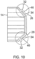
- FIG. 9 illustrates an example where the bypass diode 44 is applied to the back side of the solar cell 14, with interconnects or contacts 46 for the bypass diode 44 connected to the back layer 42 and also extending into the corner region 26 between the front and back contacts 32, 34.
- FIG. 10 illustrates a front side view of the example of FIG. 9 , with the interconnect or contact 46 for the bypass diode 44 (not shown) extending into the corner region 26 between the front and back contacts 32, 34.
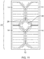
- FIG. 11 illustrates the solar cells 14 of FIGS. 9 and 10 arranged into the 2D grid of the array 22 and applied to the substrate 12, where the bypass diodes 44 (not shown) are applied to the back side of the solar cells 14, with the contacts 46 for the bypass diodes 44 extending into the corner regions 26 of the solar cells 14.
- FIGS. 7 , 8 and 11 are generalized layouts. Specifically, these layouts can be repeated across any panel 10a dimensions desired by a customer. This greatly simplifies assembly, rework, test, and inspection processes.
- the placement of the solar cell 14 and bypass diode 44 is generic
- the electrical connection of the solar cells 14 into series connections and string terminations is important customization for the end customer and is done independent of the layout.
- the front contacts 32 and back contacts 34 in the corner regions 26 of the solar cells 14 must be connected. This can be done in many combinations in order to route current through a desired path.
- Front and back contacts 32, 34 of the solar cells 14 are present in each corner region 26 for attachment to the corner conductors 20.
- Interconnects for the front and back contacts 32, 34 of each of the solar cells 14 are welded, soldered, or otherwise bonded onto the corner conductors 20 to provide a conductive path 20, 32, 34 for routing current out of the solar cells 14.
- Adjacent solar cells 14 can be electrically connected to flow current in up/down or left/right directions as desired by the specific design. Current flow can also be routed around stay-out zones as needed.
- the length or width of the solar cell array 22 can be set as desired. Also, the width can vary over the length of the array 22.
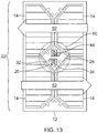
- the electrical connections are series connections that determine a flow of current through the plurality of solar cells 14. This may be accomplished by the connection schemes shown in FIGS. 12 and 13 , wherein FIG. 12 shows up/down series connections 48 between the solar cells 14 of the array 22, and FIG. 13 shows left/right series connections 50 between the solar cells 14 of the array 22. In both FIGS. 12 and 13 , these series connections 48, 50 are electrical connections between the front contacts 32 and back contacts 34 of the solar cells 14, and the bypass diodes 44, are made using the corner conductors 20 formed on or in the exposed areas 28 of the substrate 12. These series connections 48, 50 determine the current (power) flow, as indicated by the arrows 52, through the solar cells 14.
- the corner conductors 20 between solar cells 14 can be in many forms. They could be accomplished using wires that have electrical connections made on both ends, which could be from soldering, welding, conducting adhesive, or other process. In addition to wires, metal foil connectors, similar to the interconnects could be applied. Metal conductive paths or traces (not shown) can also be integrated with the substrate 12.
- this new approach attaches the solar cells 14 individually to a substrate 12 such that the corner regions 26 of two, three or four adjacent solar cells 14 are aligned on the substrate 12.
- the solar cells 14 can be laid out so that the cropped corners 24 are aligned and the corner regions 26 are adjacent, thereby exposing an area 28 of the substrate 12.
- Electrical connections between solar cells 14 are made in these corner regions 26 between front contacts 32 and back contacts 34 on the solar cells 14, bypass diodes 44, and corner conductors 20 on or in the exposed area 28 of the substrate 12, wherein these conductive paths are used to create a string of solar cells 14 in a series connection 48, 50 comprising a circuit.
- a rework and repair process is necessary for the 2D grid of the array 22, and it is not clear how that is achieved using existing techniques. For example, the extraction and replacement of components may result in a second electrical interconnect made in the same location as a first electrical interconnect, and such a repeated connection may not have sufficient strength.
- This disclosure describes a connector design that simplifies rework of these items, and facilitates repairs of the solar cell array 22. Specifically, an electrical connection is repaired by removing a first interconnect in a first location in the electrical connection and by forming a second interconnect in a second location in the electrical connection different from the first location.
- the second location may be adjacent the first location, for example, when an area used for the electrical connection is large enough to encompass both the first and second locations and to allow electrical current to flow around the first location.
- FIG. 14 further illustrates a connection scheme between a plurality of solar cells 14, according to one example.
- the connection scheme shown comprises up/down series connections 48 between the front contacts 32 and back contacts 34 of the solar cells 14, and the bypass diodes 44, made in the exposed areas 28 of the substrate 12, using the corner conductors 20. These series connections 48 determine the flow of current, as indicated by the arrows 52, through the solar cells 14.
- One or more conductor elements may be added to or removed from the corner region 26 to select current pathways for the solar cells 14.
- the conductor element comprises a jumper 54a, 54b that allows circuits to be terminated at the corner regions 26 or to direct current to the next solar cell 14.
- the jumpers 54a, 54b bridge the electrical connections from at least one of the corner conductors 20 to one or more other conductive paths.
- Each jumper 54a, 54b is a metal foil interconnect that is similar to existing metal interconnects used in solar cell panels 10.
- each jumper 54a, 54b has a shape comprised of two flange elements with parallel planes connected by a web element, which enables multiple connection points.
- the jumper 22 could be welded, soldered, or joined by other methods, onto the conducting paths and connection pads.
- Other types of conductive elements, such as wires, as well as other shapes, could also be employed.
- FIG. 14 shows a jumper 54a that connects the back contact 34 of the top left solar cell 14 to the front contact 32 of the bottom left solar cell 14.
- This jumper 54a also connects through the bypass diode 44 to the back contact 34 of the bottom left solar cell 14.
- This connection path provides for the current flow 52 from top to bottom shown on the left side of the figure.
- a similar configuration using jumper 54b provides for the current flow 52 from bottom to top shown on the right side of the figure.
- this structure is significant. Now, there is a single printed corner conductor 20 pattern, single layout of solar cells 14, and single layout of bypass diodes 44. This single configuration has great advantages for automation of manufacturing, testing, and inspection.
- the application of a jumper 54a, 54b provides for a simple way to control the number of solar cells 14 in a circuit.
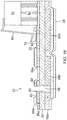
- FIG. 15 shows a side view of an example wherein the substrate 12 is a flex sheet assembly, according to one example.
- the substrate 12 includes a polyimide base layer 54 with Copper (Cu) layer 56a above and Cu layer 56b below, wherein Cu layers 56a and 56b form a multilayer conductor.
- a conducting back sheet of polyimide 58 can be applied to the substrate 12, which is useful in a space environment in that it will reduce the accumulation of charge.
- Another capability is the addition of a plated Silver (Ag) or Gold (Au) layer 60 on the Cu layer 56a, which improves the ability to make connections.
- the Cu layer 56a with plated Ag or Au layer 60 is patterned as the corner conductors 20, and the Cu layer 56b is patterned to form buried conductors within the substrate 12, including, for example, power and common lines.
- the solar cell 14 Shown on the right side is the solar cell 14 that is attached to the substrate 12 with adhesive 62. Also visible is the metal foil interconnect 64 attached to the solar cell 14 and the plated Ag or Au layer 60 of the corner conductors 20. This is a rather typical construction and assembly that could form the structures presented in earlier figures.
- the substrate 12 also includes insulating layers that separate at least one of the multilayer conductors 56a, 56b from at least another one of the multilayer conductors 56a, 56b.
- insulating layers that separate at least one of the multilayer conductors 56a, 56b from at least another one of the multilayer conductors 56a, 56b.
- Polyimide has a high breakdown strength, greater than air or vacuum, and the polyimide overlay layers 66a, 66b are useful for preventing electrostatic discharge (ESD), which is an important concern in the space environment. Furthermore, this enables corner conductors 20 to pass under the solar cell 14.
- the adhesive 62 is non-conducting, but the continuous polyimide layer of the polyimide overlay layers 66a, 66b offers significant protection against shorting between buried conductors in Cu layers 56a, 56b and the solar cell 14.
- the top polyimide overlay layer 66a may be omitted underneath the solar cell 14. This may be advantageous if the top polyimide overlay layer 66a is prone to bubbles or other defects.
- the top polyimide overlay layer 66a there is an alignment between Cu layer 56a, Cu layer 56b and the top polyimide overlay layer 66a.
- the top polyimide overlay layer 66a almost fully encases the Cu layer 56a, polyimide layer 54, and Cu layer 56b, with only small access holes to the Cu layer 56a and Cu layer 56b. This requires the top polyimide overlay layer 66a to roll up and over the corners of the Cu layers 56a and 56b.
- the top polyimide overlay layer 66a provides valuable protection against ESD.
- the top polyimide overlay layer 66a has larger holes to avoid overlapping the edges of the Cu layers 56a and 56b. This top polyimide overlay layer 66a may be easier to fabricate with less defects than a full top polyimide overlay layer 66a.
- top polyimide overlay layer 66a may not be needed; in that case, there would be no hindrance of the top polyimide overlay layer 66a to any jumper 54 connection.
- a jumper 54 may connect directly from the Cu layer 56a to the Cu layer 56b. This eliminates the Cu-plated via 68 connections, which could be a reliability concern, especially in the flex sheet assembly.
- the thickness of the top polyimide overlay layer 66a is typically about ⁇ 0.1 mm, while the length of the jumper 54 typically may be about ⁇ 4 mm. Having the metal of the jumper 54 surrounded by large amounts of polyimide from the top polyimide overlay layer 66a may impede the jumper 54, but will also impede ESD, which can be valuable.
- electrical access is provided to the buried Cu layer 56b. This could be accomplished with the via 68 connection between Cu layer 56a and Cu layer 56b, or with a direct connection between Cu layer 56a and Cu layer 56b. Also, there may be multiple connections between Cu layer 56a and Cu layer 56b. This redundancy is an important attribute and can be employed when possible.
- the traces of the Cu layers 56a, 56b can be broadened into wider conductors, power lines and common lines that do not have the insulating polyimide layers 66a, 66b between them.
- there is more Copper used for conduction which reduces resistance losses. This does reduce the number of discrete conductors; however, the connection redundancy is preserved.
- FIG. 16 illustrates an example where the metal foil interconnect 64 from the solar cell 14 has separated from the plated Ag or Au layer 60 and/or Cu layer 56a.
- This separation may be the defect causing the rework process.
- a cracked solar cell 14 would need to be removed including the interconnections to the substrate 12.
- the separation results in a change in the surface region of the plated Ag or Au layer 60 and/or Cu layer 56a, for example, resulting in some debris 70, such as solder residue, roughness, etc.
- FIG. 17 shows one proposed process for repairing the substrate 12 in the example of FIG. 16 , wherein an area of the plated Ag or Au layer 60 and/or Cu layer 56a used for the electrical connection is large enough that one or more additional connections can be made in the area
- the replacement solar cell 14 is attached to the flex sheet substrate 12 using adhesive 62, and the replacement interconnect 64 extends from the replacement solar cell 14 to make contact with the plated Ag or Au layer 60 and/or Cu layer 56a in an adjacent location that avoids the original connection region.
- the adjacent location in this example has enough conductor for electrical current to flow around the damaged region.
- an electrical connection is repaired by removing a first interconnect 64 in a first location in the electrical connection and by forming a second interconnect 64 in a second location in the electrical connection different from the first location.
- the second location may be adjacent the first location, for example, when the plated Ag or Au layer 60 and/or Cu layer 56a comprise a connection pad that is large enough to encompass both the first and second locations and to allow electrical current to flow around the first location.
- the first interconnect 64 in the first location is completely removed, while in another example, a joint remains when the first interconnect 64 is removed.
- a replacement solar cell 14 is attached to the flex sheet substrate 12 using adhesive 62, and a replacement interconnect 64 extends from the replacement solar cell 14 to make contact with the plated Ag or Au layer 60 and/or Cu layer 56a in an adjacent location that avoids the original connection region, wherein the adjacent location has enough conductor for electrical current to flow around the damaged region.
- a replacement interconnect 64 is attached to the plated Ag or Au layer 60 and/or Cu layer 56a in an adjacent location that avoids the original connection region, wherein the adjacent location has enough conductor for electrical current to flow around the joint of the interconnect 64. Maintaining the joint of the interconnect 64 may be preferred as this avoids damage to the plated Ag or Au layer 60 and/or Cu layer 56a, for example, by rupturing or divoting.
- a first type of repair components could be used in connecting a solar cell 14 or bypass diode 44 to the substrate 12, while a second type of repair components could be used to connect pairs of corner conductors 20 on the substrate 12.
- the first type of repair components would be the standard interconnects 64
- the second type of repair components would be variations of the standard interconnects 64 used for the repair process, i.e., replacement interconnects 64, which have a slightly different structure that moves the electrical connection to an adjacent location from the original connection. It is desirable to position the initial and rework connection points, such that debris 70, cut interconnect 64, or rupturing or divoting of the plated Ag or Au layer 60 and/or Cu layer 56a, does not impact repair assembly or current flow.
- Another variation is where the type of repair components is designed to allow initial and rework connections to be made using the same interconnect 64 structure. Thus, a single interconnect 64 is needed. This interconnect 64 is used for both the initial build and for rework. There would be initial and rework pairs of connection points on the plated Ag or Au layer 60 and/or Cu layer 56a for the initial and rework connections. Again, it is desirable to design these parts and the conducting path on the substrate 12, such that rupture of the conducting path on the substrate 12 does not impact conductivity after rework.
- this interconnect design enables an additional connection point to be used.
- the interconnect 64 can be left in place and an adjacent location of the plated Ag or Au layer 60 and/or Cu layer 56a can be used to provide greater reliability. This avoids the possibility of further damage during the rework process.
- FIG. 18 shows how repair components 72 are used, according to one example.
- the repair components 72 comprise replacement interconnects 64 connecting the front or back contacts 32, 34 to the corner conductors 20, or replacement interconnects 64 connecting the bypass diodes 44 to the corner conductors 20, or jumpers 54 connecting the corner conductors 20.
- the following steps are performed: separate interconnects 64 at a weld joint, clean out the solar cell 14 and/or bypass diode 44, replace the solar cell 14 and/or bypass diode 44 with a repair unit, and weld the interconnects 64 at adjacent locations to the corner conductors 20 or front and back contacts 32, 34, or connect a jumper 54 between corner conductors 20, wherein all work is performed on a top side of the assembly with no components sticking up.
- all the electrical connections in this assembly are made by overlapping metal layers. Then, a joint is formed by access from the top for solder or weld processes (laser, resistive, ultrasonic, etc.). This access is very straightforward, as there is no overlapping or folding of conductors. Also, the repair has no material sticking up higher than the original assembly, which is a concern for space solar panels 10a that are often folded tightly for stowage and launch.
- Examples of the disclosure may be described in the context of a method 74 of fabricating a solar cell 14, solar cell panel 10a and/or satellite, comprising steps 76-88, as shown in FIG. 19 , wherein the resulting satellite 90 having a solar cell panel 10a comprised of solar cells 14 are shown in FIG. 20 .
- exemplary method 74 may include specification and design 76 of the solar cell 14, solar cell panel 10a and/or satellite 90, and material procurement 78 for same.
- component and subassembly manufacturing 80 and system integration 82 of the solar cell 14, solar cell panel 10a and/or satellite 90 takes place, which include fabricating the solar cell 14, solar cell panel 10a and/or satellite 90.
- the solar cell 14, solar cell panel 10a and/or satellite 90 may go through certification and delivery 84 in order to be placed in service 86.
- the solar cell 14, solar cell panel 10a and/or satellite 90 may also be scheduled for maintenance and service 88 (which includes modification, reconfiguration, refurbishment, and so on), before being launched.
- Each of the processes of method 74 may be performed or carried out by a system integrator, a third party, and/or an operator (e.g., a customer).
- a system integrator may include without limitation any number of solar cell, solar cell panel, satellite or spacecraft manufacturers and major-system subcontractors;
- a third party may include without limitation any number of venders, subcontractors, and suppliers; and
- an operator may be a satellite company, military entity, service organization, and so on.
- a satellite 90 fabricated by exemplary method 74 may include systems 92, a body 94, solar cell panels 10a comprised of solar cells 14, and one or more antennae 96.
- the systems 92 included with the satellite 90 include, but are not limited to, one or more of a propulsion system 98, an electrical system 100, a communications system 102, and a power system 104. Any number of other systems 92 also may be included.
- FIG. 21 is an illustration of the solar cell panel 10a in the form of a functional block diagram, according to one example.
- the solar cell panel 10a is comprised of the solar cell array 22, which is comprised of one or more of the solar cells 14 individually attached to the substrate 12.
- Each of the solar cells 14 absorbs light 106 from a light source 108 and generates an electrical output 110 in response thereto.
- At least one of the solar cells 14 has at least one cropped corner 24 that defines a corner region 26, such that an area 28 of the substrate 12 remains exposed when the solar cell 14 is attached to the substrate 12.
- the corner regions 26 of adjacent ones of the solar cells 14 are aligned, thereby exposing the area 28 of the substrate 12.
- the area 28 of the substrate 12 that remains exposed includes one or more corner conductors 20 attached to, printed on, or integrated with the substrate 12, and one or more electrical connections between the solar cells 14 and the corner conductors 20 are made in a corner region 26 resulting from the cropped corner 24 of the at least one of the solar cells 14.
- the corner region 26 resulting from the cropped corner 24 includes at least one contact, for example, a front contact 32 on a front side of the solar cell 14 and/or a back contact 34 on a back side of the solar cell 14, for making the electrical connections between the corner conductors 20 and the solar cell 14.
- the electrical connections may comprise up/down or left/right series connections that determine a flow of power through the solar cells 14, and may include one or more bypass diodes 44.
Landscapes
- Photovoltaic Devices (AREA)
Priority Applications (1)
| Application Number | Priority Date | Filing Date | Title |
|---|---|---|---|
| EP23178386.1A EP4235810A3 (fr) | 2016-09-14 | 2017-09-14 | Recyclage et réparation de composants dans un réseau de piles solaires |
Applications Claiming Priority (19)
| Application Number | Priority Date | Filing Date | Title |
|---|---|---|---|
| US201662394636P | 2016-09-14 | 2016-09-14 | |
| US201662394667P | 2016-09-14 | 2016-09-14 | |
| US201662394629P | 2016-09-14 | 2016-09-14 | |
| US201662394616P | 2016-09-14 | 2016-09-14 | |
| US201662394666P | 2016-09-14 | 2016-09-14 | |
| US201662394649P | 2016-09-14 | 2016-09-14 | |
| US201662394641P | 2016-09-14 | 2016-09-14 | |
| US201662394623P | 2016-09-14 | 2016-09-14 | |
| US201662394632P | 2016-09-14 | 2016-09-14 | |
| US201662394627P | 2016-09-14 | 2016-09-14 | |
| US201662394671P | 2016-09-14 | 2016-09-14 | |
| US201662394672P | 2016-09-14 | 2016-09-14 | |
| US15/643,279 US20180076348A1 (en) | 2016-09-14 | 2017-07-06 | Rework and repair of components in a solar cell array |
| US15/643,285 US20180076761A1 (en) | 2016-09-14 | 2017-07-06 | Power routing module with a switching matrix for a solar cell array |
| US15/643,287 US10763383B2 (en) | 2016-09-14 | 2017-07-06 | Nano-metal connections for a solar cell array |
| US15/643,274 US20180076346A1 (en) | 2016-09-14 | 2017-07-06 | Solar cell array connections using corner conductors |
| US15/643,277 US12615851B2 (en) | 2016-09-14 | 2017-07-06 | Prefabricated conductors on a substrate to facilitate corner connections for a solar cell array |
| US15/643,289 US11437533B2 (en) | 2016-09-14 | 2017-07-06 | Solar cells for a solar cell array |
| US15/643,282 US20180076349A1 (en) | 2016-09-14 | 2017-07-06 | Power routing module for a solar cell array |
Related Child Applications (2)
| Application Number | Title | Priority Date | Filing Date |
|---|---|---|---|
| EP23178386.1A Division-Into EP4235810A3 (fr) | 2016-09-14 | 2017-09-14 | Recyclage et réparation de composants dans un réseau de piles solaires |
| EP23178386.1A Division EP4235810A3 (fr) | 2016-09-14 | 2017-09-14 | Recyclage et réparation de composants dans un réseau de piles solaires |
Publications (2)
| Publication Number | Publication Date |
|---|---|
| EP3297033A1 true EP3297033A1 (fr) | 2018-03-21 |
| EP3297033B1 EP3297033B1 (fr) | 2025-01-08 |
Family
ID=59858998
Family Applications (7)
| Application Number | Title | Priority Date | Filing Date |
|---|---|---|---|
| EP17191166.2A Active EP3297034B1 (fr) | 2016-09-14 | 2017-09-14 | Connexions nano-métalliques pour réseau de cellules solaires |
| EP17191162.1A Active EP3297042B1 (fr) | 2016-09-14 | 2017-09-14 | Module d'acheminement de puissance avec une matrice de commutation pour un réseau de cellules solaires |
| EP17191168.8A Active EP3297035B1 (fr) | 2016-09-14 | 2017-09-14 | Connexions de réseau de cellules solaires au moyen de conducteurs d'angle |
| EP17191154.8A Active EP3297033B1 (fr) | 2016-09-14 | 2017-09-14 | Recyclage et réparation de composants dans un réseau de piles solaires |
| EP21174069.1A Pending EP3907766A1 (fr) | 2016-09-14 | 2017-09-14 | Connexions de réseau de cellules solaires au moyen de conducteurs d'angle |
| EP17191134.0A Active EP3297032B1 (fr) | 2016-09-14 | 2017-09-14 | Conducteurs préfabriqués sur un substrat pour faciliter des connexions d'angle pour un réseau de cellules solaires |
| EP17191159.7A Active EP3297041B1 (fr) | 2016-09-14 | 2017-09-14 | Module d'acheminement de puissance pour un réseau de cellules solaires |
Family Applications Before (3)
| Application Number | Title | Priority Date | Filing Date |
|---|---|---|---|
| EP17191166.2A Active EP3297034B1 (fr) | 2016-09-14 | 2017-09-14 | Connexions nano-métalliques pour réseau de cellules solaires |
| EP17191162.1A Active EP3297042B1 (fr) | 2016-09-14 | 2017-09-14 | Module d'acheminement de puissance avec une matrice de commutation pour un réseau de cellules solaires |
| EP17191168.8A Active EP3297035B1 (fr) | 2016-09-14 | 2017-09-14 | Connexions de réseau de cellules solaires au moyen de conducteurs d'angle |
Family Applications After (3)
| Application Number | Title | Priority Date | Filing Date |
|---|---|---|---|
| EP21174069.1A Pending EP3907766A1 (fr) | 2016-09-14 | 2017-09-14 | Connexions de réseau de cellules solaires au moyen de conducteurs d'angle |
| EP17191134.0A Active EP3297032B1 (fr) | 2016-09-14 | 2017-09-14 | Conducteurs préfabriqués sur un substrat pour faciliter des connexions d'angle pour un réseau de cellules solaires |
| EP17191159.7A Active EP3297041B1 (fr) | 2016-09-14 | 2017-09-14 | Module d'acheminement de puissance pour un réseau de cellules solaires |
Country Status (1)
| Country | Link |
|---|---|
| EP (7) | EP3297034B1 (fr) |
Families Citing this family (10)
| Publication number | Priority date | Publication date | Assignee | Title |
|---|---|---|---|---|
| US20180076761A1 (en) | 2016-09-14 | 2018-03-15 | The Boeing Company | Power routing module with a switching matrix for a solar cell array |
| US10763383B2 (en) | 2016-09-14 | 2020-09-01 | The Boeing Company | Nano-metal connections for a solar cell array |
| US12490523B2 (en) * | 2017-06-12 | 2025-12-02 | The Boeing Company | Solar cell array with changeable string length |
| US20180358491A1 (en) * | 2017-06-12 | 2018-12-13 | The Boeing Company | Solar cell array with bypassed solar cells |
| US12244265B2 (en) | 2018-03-28 | 2025-03-04 | The Boeing Company | Wiring for a rigid panel solar array |
| US11967923B2 (en) | 2018-03-28 | 2024-04-23 | The Boeing Company | Single sheet foldout solar array |
| CN108598188B (zh) * | 2018-05-08 | 2020-02-07 | 英利能源(中国)有限公司 | N型背接触太阳能电池的制备方法及太阳能电池 |
| CN110265488B (zh) * | 2019-06-26 | 2021-03-30 | 重庆西南集成电路设计有限责任公司 | 内嵌光伏旁路开关的光伏电池组件 |
| US20220165899A1 (en) * | 2020-11-21 | 2022-05-26 | The Boeing Company | Space solar cell array with custom voltage |
| CN114373816B (zh) * | 2021-12-28 | 2022-07-26 | 北京博瑞原子空间能源科技有限公司 | 一种太阳阵及其制备方法与应用 |
Citations (3)
| Publication number | Priority date | Publication date | Assignee | Title |
|---|---|---|---|---|
| US5567248A (en) * | 1995-09-05 | 1996-10-22 | Chung; Darius | Modular solar cell contact arrangement |
| EP1548847A2 (fr) * | 2003-12-23 | 2005-06-29 | Alcatel | Panneau de générateur solaire et satellite associé |
| US20150144173A1 (en) * | 2013-11-27 | 2015-05-28 | Space Systems/Loral, Llc | Integral corner bypass diode interconnecting configuration for multiple solar cells |
Family Cites Families (17)
| Publication number | Priority date | Publication date | Assignee | Title |
|---|---|---|---|---|
| US5391235A (en) * | 1992-03-31 | 1995-02-21 | Canon Kabushiki Kaisha | Solar cell module and method of manufacturing the same |
| US6313396B1 (en) * | 2000-05-22 | 2001-11-06 | The Boeing Company | Lightweight solar module and method of fabrication |
| DE10136442A1 (de) * | 2001-07-26 | 2003-02-13 | Ralf Adelhelm | Kontakte und Verbinder von Solarzellen |
| US7245134B2 (en) * | 2005-01-31 | 2007-07-17 | Formfactor, Inc. | Probe card assembly including a programmable device to selectively route signals from channels of a test system controller to probes |
| KR100735395B1 (ko) * | 2005-05-10 | 2007-07-04 | 삼성전자주식회사 | 집적 회로를 이용한 인쇄회로기판의 라우팅 방법 |
| US20080142071A1 (en) * | 2006-12-15 | 2008-06-19 | Miasole | Protovoltaic module utilizing a flex circuit for reconfiguration |
| US20090025778A1 (en) * | 2007-07-23 | 2009-01-29 | Day4 Energy Inc. | Shading protection for solar cells and solar cell modules |
| US20100186795A1 (en) * | 2009-01-28 | 2010-07-29 | Stephen Joseph Gaul | Connection systems and methods for solar cells |
| US20110083716A1 (en) * | 2009-07-22 | 2011-04-14 | Applied Materials, Inc. | Monolithic module assembly using back contact solar cells and metal ribbon |
| JP2011071214A (ja) * | 2009-09-24 | 2011-04-07 | Kaneka Corp | 太陽電池モジュール |
| JP2011108969A (ja) * | 2009-11-20 | 2011-06-02 | Hitachi Cable Ltd | 太陽電池モジュールの製造方法、及び太陽電池用配線基板 |
| US20110139184A1 (en) * | 2009-12-16 | 2011-06-16 | Nagendra Srinivas Cherukupalli | Systems, Circuits, and Methods for an Intelligent Cleaning System for an Adaptive Solar Power System |
| US8604330B1 (en) * | 2010-12-06 | 2013-12-10 | 4Power, Llc | High-efficiency solar-cell arrays with integrated devices and methods for forming them |
| EP2833416B1 (fr) * | 2012-03-30 | 2021-11-10 | DSM Advanced Solar B.V. | Module de cellules solaires type à contact arrière |
| JP2015065395A (ja) * | 2013-08-28 | 2015-04-09 | 矢崎総業株式会社 | ジャンパモジュール搭載回路基板および回路基板組立体 |
| FR3024591B1 (fr) * | 2014-07-29 | 2016-08-05 | Bubendorff | Procede de fabrication d’un panneau photovoltaique |
| US20160218665A1 (en) * | 2015-01-22 | 2016-07-28 | Solaero Technologies Corp. | Space solar cell panel with blocking diodes |
-
2017
- 2017-09-14 EP EP17191166.2A patent/EP3297034B1/fr active Active
- 2017-09-14 EP EP17191162.1A patent/EP3297042B1/fr active Active
- 2017-09-14 EP EP17191168.8A patent/EP3297035B1/fr active Active
- 2017-09-14 EP EP17191154.8A patent/EP3297033B1/fr active Active
- 2017-09-14 EP EP21174069.1A patent/EP3907766A1/fr active Pending
- 2017-09-14 EP EP17191134.0A patent/EP3297032B1/fr active Active
- 2017-09-14 EP EP17191159.7A patent/EP3297041B1/fr active Active
Patent Citations (3)
| Publication number | Priority date | Publication date | Assignee | Title |
|---|---|---|---|---|
| US5567248A (en) * | 1995-09-05 | 1996-10-22 | Chung; Darius | Modular solar cell contact arrangement |
| EP1548847A2 (fr) * | 2003-12-23 | 2005-06-29 | Alcatel | Panneau de générateur solaire et satellite associé |
| US20150144173A1 (en) * | 2013-11-27 | 2015-05-28 | Space Systems/Loral, Llc | Integral corner bypass diode interconnecting configuration for multiple solar cells |
Also Published As
| Publication number | Publication date |
|---|---|
| EP3297042B1 (fr) | 2023-05-10 |
| EP3297033B1 (fr) | 2025-01-08 |
| EP3297041A1 (fr) | 2018-03-21 |
| EP3297034A1 (fr) | 2018-03-21 |
| EP3297035A1 (fr) | 2018-03-21 |
| EP3297034B1 (fr) | 2023-11-22 |
| EP3297032B1 (fr) | 2023-05-10 |
| EP3297041B1 (fr) | 2023-11-22 |
| EP3297042A1 (fr) | 2018-03-21 |
| EP3297035B1 (fr) | 2021-08-04 |
| EP3907766A1 (fr) | 2021-11-10 |
| EP3297032A1 (fr) | 2018-03-21 |
Similar Documents
| Publication | Publication Date | Title |
|---|---|---|
| JP7624423B2 (ja) | ソーラーセルアレイ内の構成要素の改修及び修理 | |
| EP3297033B1 (fr) | Recyclage et réparation de composants dans un réseau de piles solaires | |
| US20180076348A1 (en) | Rework and repair of components in a solar cell array | |
| EP3297040B1 (fr) | Cellules solaires pour un réseau de cellules solaires | |
| EP4521885A2 (fr) | Cellules solaires pour un réseau de cellules solaires | |
| US20220165899A1 (en) | Space solar cell array with custom voltage |
Legal Events
| Date | Code | Title | Description |
|---|---|---|---|
| PUAI | Public reference made under article 153(3) epc to a published international application that has entered the european phase |
Free format text: ORIGINAL CODE: 0009012 |
|
| STAA | Information on the status of an ep patent application or granted ep patent |
Free format text: STATUS: REQUEST FOR EXAMINATION WAS MADE |
|
| 17P | Request for examination filed |
Effective date: 20170914 |
|
| AK | Designated contracting states |
Kind code of ref document: A1 Designated state(s): AL AT BE BG CH CY CZ DE DK EE ES FI FR GB GR HR HU IE IS IT LI LT LU LV MC MK MT NL NO PL PT RO RS SE SI SK SM TR |
|
| AX | Request for extension of the european patent |
Extension state: BA ME |
|
| STAA | Information on the status of an ep patent application or granted ep patent |
Free format text: STATUS: EXAMINATION IS IN PROGRESS |
|
| 17Q | First examination report despatched |
Effective date: 20201201 |
|
| REG | Reference to a national code |
Ref country code: DE Ref legal event code: R079 Free format text: PREVIOUS MAIN CLASS: H01L0031020000 Ipc: H01L0031050000 Ref country code: DE Ref legal event code: R079 Ref document number: 602017087216 Country of ref document: DE Free format text: PREVIOUS MAIN CLASS: H01L0031020000 Ipc: H01L0031050000 |
|
| GRAP | Despatch of communication of intention to grant a patent |
Free format text: ORIGINAL CODE: EPIDOSNIGR1 |
|
| STAA | Information on the status of an ep patent application or granted ep patent |
Free format text: STATUS: GRANT OF PATENT IS INTENDED |
|
| RIC1 | Information provided on ipc code assigned before grant |
Ipc: H01L 31/042 20140101ALI20221015BHEP Ipc: H01L 31/0687 20120101ALI20221015BHEP Ipc: H01L 31/0352 20060101ALI20221015BHEP Ipc: H01L 31/05 20140101AFI20221015BHEP |
|
| INTG | Intention to grant announced |
Effective date: 20221122 |
|
| GRAJ | Information related to disapproval of communication of intention to grant by the applicant or resumption of examination proceedings by the epo deleted |
Free format text: ORIGINAL CODE: EPIDOSDIGR1 |
|
| STAA | Information on the status of an ep patent application or granted ep patent |
Free format text: STATUS: EXAMINATION IS IN PROGRESS |
|
| GRAP | Despatch of communication of intention to grant a patent |
Free format text: ORIGINAL CODE: EPIDOSNIGR1 |
|
| STAA | Information on the status of an ep patent application or granted ep patent |
Free format text: STATUS: GRANT OF PATENT IS INTENDED |
|
| INTC | Intention to grant announced (deleted) | ||
| INTG | Intention to grant announced |
Effective date: 20230131 |
|
| RAP3 | Party data changed (applicant data changed or rights of an application transferred) |
Owner name: THE BOEING COMPANY |
|
| GRAJ | Information related to disapproval of communication of intention to grant by the applicant or resumption of examination proceedings by the epo deleted |
Free format text: ORIGINAL CODE: EPIDOSDIGR1 |
|
| STAA | Information on the status of an ep patent application or granted ep patent |
Free format text: STATUS: EXAMINATION IS IN PROGRESS |
|
| P01 | Opt-out of the competence of the unified patent court (upc) registered |
Effective date: 20230509 |
|
| INTC | Intention to grant announced (deleted) | ||
| GRAP | Despatch of communication of intention to grant a patent |
Free format text: ORIGINAL CODE: EPIDOSNIGR1 |
|
| STAA | Information on the status of an ep patent application or granted ep patent |
Free format text: STATUS: GRANT OF PATENT IS INTENDED |
|
| INTG | Intention to grant announced |
Effective date: 20240117 |
|
| GRAJ | Information related to disapproval of communication of intention to grant by the applicant or resumption of examination proceedings by the epo deleted |
Free format text: ORIGINAL CODE: EPIDOSDIGR1 |
|
| STAA | Information on the status of an ep patent application or granted ep patent |
Free format text: STATUS: EXAMINATION IS IN PROGRESS |
|
| INTC | Intention to grant announced (deleted) | ||
| GRAP | Despatch of communication of intention to grant a patent |
Free format text: ORIGINAL CODE: EPIDOSNIGR1 |
|
| STAA | Information on the status of an ep patent application or granted ep patent |
Free format text: STATUS: GRANT OF PATENT IS INTENDED |
|
| RIC1 | Information provided on ipc code assigned before grant |
Ipc: H01L 31/0687 20120101ALI20240819BHEP Ipc: H01L 31/044 20140101ALI20240819BHEP Ipc: H01L 31/042 20140101ALI20240819BHEP Ipc: H01L 31/041 20140101ALI20240819BHEP Ipc: H01L 31/0352 20060101ALI20240819BHEP Ipc: H01L 31/05 20140101AFI20240819BHEP |
|
| INTG | Intention to grant announced |
Effective date: 20240910 |
|
| GRAS | Grant fee paid |
Free format text: ORIGINAL CODE: EPIDOSNIGR3 |
|
| GRAA | (expected) grant |
Free format text: ORIGINAL CODE: 0009210 |
|
| STAA | Information on the status of an ep patent application or granted ep patent |
Free format text: STATUS: THE PATENT HAS BEEN GRANTED |
|
| AK | Designated contracting states |
Kind code of ref document: B1 Designated state(s): AL AT BE BG CH CY CZ DE DK EE ES FI FR GB GR HR HU IE IS IT LI LT LU LV MC MK MT NL NO PL PT RO RS SE SI SK SM TR |
|
| REG | Reference to a national code |
Ref country code: GB Ref legal event code: FG4D |
|
| REG | Reference to a national code |
Ref country code: CH Ref legal event code: EP |
|
| REG | Reference to a national code |
Ref country code: DE Ref legal event code: R096 Ref document number: 602017087216 Country of ref document: DE |
|
| REG | Reference to a national code |
Ref country code: IE Ref legal event code: FG4D Ref country code: NL Ref legal event code: FP |
|
| REG | Reference to a national code |
Ref country code: LT Ref legal event code: MG9D |
|
| REG | Reference to a national code |
Ref country code: AT Ref legal event code: MK05 Ref document number: 1758922 Country of ref document: AT Kind code of ref document: T Effective date: 20250108 |
|
| PG25 | Lapsed in a contracting state [announced via postgrant information from national office to epo] |
Ref country code: RS Free format text: LAPSE BECAUSE OF FAILURE TO SUBMIT A TRANSLATION OF THE DESCRIPTION OR TO PAY THE FEE WITHIN THE PRESCRIBED TIME-LIMIT Effective date: 20250408 |
|
| PG25 | Lapsed in a contracting state [announced via postgrant information from national office to epo] |
Ref country code: FI Free format text: LAPSE BECAUSE OF FAILURE TO SUBMIT A TRANSLATION OF THE DESCRIPTION OR TO PAY THE FEE WITHIN THE PRESCRIBED TIME-LIMIT Effective date: 20250108 |
|
| PG25 | Lapsed in a contracting state [announced via postgrant information from national office to epo] |
Ref country code: PL Free format text: LAPSE BECAUSE OF FAILURE TO SUBMIT A TRANSLATION OF THE DESCRIPTION OR TO PAY THE FEE WITHIN THE PRESCRIBED TIME-LIMIT Effective date: 20250108 |
|
| PG25 | Lapsed in a contracting state [announced via postgrant information from national office to epo] |
Ref country code: NO Free format text: LAPSE BECAUSE OF FAILURE TO SUBMIT A TRANSLATION OF THE DESCRIPTION OR TO PAY THE FEE WITHIN THE PRESCRIBED TIME-LIMIT Effective date: 20250408 Ref country code: IS Free format text: LAPSE BECAUSE OF FAILURE TO SUBMIT A TRANSLATION OF THE DESCRIPTION OR TO PAY THE FEE WITHIN THE PRESCRIBED TIME-LIMIT Effective date: 20250508 |
|
| PG25 | Lapsed in a contracting state [announced via postgrant information from national office to epo] |
Ref country code: HR Free format text: LAPSE BECAUSE OF FAILURE TO SUBMIT A TRANSLATION OF THE DESCRIPTION OR TO PAY THE FEE WITHIN THE PRESCRIBED TIME-LIMIT Effective date: 20250108 |
|
| PG25 | Lapsed in a contracting state [announced via postgrant information from national office to epo] |
Ref country code: LV Free format text: LAPSE BECAUSE OF FAILURE TO SUBMIT A TRANSLATION OF THE DESCRIPTION OR TO PAY THE FEE WITHIN THE PRESCRIBED TIME-LIMIT Effective date: 20250108 Ref country code: PT Free format text: LAPSE BECAUSE OF FAILURE TO SUBMIT A TRANSLATION OF THE DESCRIPTION OR TO PAY THE FEE WITHIN THE PRESCRIBED TIME-LIMIT Effective date: 20250508 |
|
| PG25 | Lapsed in a contracting state [announced via postgrant information from national office to epo] |
Ref country code: BG Free format text: LAPSE BECAUSE OF FAILURE TO SUBMIT A TRANSLATION OF THE DESCRIPTION OR TO PAY THE FEE WITHIN THE PRESCRIBED TIME-LIMIT Effective date: 20250108 Ref country code: GR Free format text: LAPSE BECAUSE OF FAILURE TO SUBMIT A TRANSLATION OF THE DESCRIPTION OR TO PAY THE FEE WITHIN THE PRESCRIBED TIME-LIMIT Effective date: 20250409 |
|
| PG25 | Lapsed in a contracting state [announced via postgrant information from national office to epo] |
Ref country code: AT Free format text: LAPSE BECAUSE OF FAILURE TO SUBMIT A TRANSLATION OF THE DESCRIPTION OR TO PAY THE FEE WITHIN THE PRESCRIBED TIME-LIMIT Effective date: 20250108 |
|
| PG25 | Lapsed in a contracting state [announced via postgrant information from national office to epo] |
Ref country code: SE Free format text: LAPSE BECAUSE OF FAILURE TO SUBMIT A TRANSLATION OF THE DESCRIPTION OR TO PAY THE FEE WITHIN THE PRESCRIBED TIME-LIMIT Effective date: 20250108 |
|
| PG25 | Lapsed in a contracting state [announced via postgrant information from national office to epo] |
Ref country code: SM Free format text: LAPSE BECAUSE OF FAILURE TO SUBMIT A TRANSLATION OF THE DESCRIPTION OR TO PAY THE FEE WITHIN THE PRESCRIBED TIME-LIMIT Effective date: 20250108 |
|
| REG | Reference to a national code |
Ref country code: DE Ref legal event code: R097 Ref document number: 602017087216 Country of ref document: DE |
|
| PG25 | Lapsed in a contracting state [announced via postgrant information from national office to epo] |
Ref country code: DK Free format text: LAPSE BECAUSE OF FAILURE TO SUBMIT A TRANSLATION OF THE DESCRIPTION OR TO PAY THE FEE WITHIN THE PRESCRIBED TIME-LIMIT Effective date: 20250108 |
|
| PGFP | Annual fee paid to national office [announced via postgrant information from national office to epo] |
Ref country code: DE Payment date: 20250929 Year of fee payment: 9 |
|
| PGFP | Annual fee paid to national office [announced via postgrant information from national office to epo] |
Ref country code: NL Payment date: 20250926 Year of fee payment: 9 |
|
| PGFP | Annual fee paid to national office [announced via postgrant information from national office to epo] |
Ref country code: BE Payment date: 20250929 Year of fee payment: 9 Ref country code: GB Payment date: 20250929 Year of fee payment: 9 |
|
| PGFP | Annual fee paid to national office [announced via postgrant information from national office to epo] |
Ref country code: FR Payment date: 20250925 Year of fee payment: 9 |
|
| PG25 | Lapsed in a contracting state [announced via postgrant information from national office to epo] |
Ref country code: EE Free format text: LAPSE BECAUSE OF FAILURE TO SUBMIT A TRANSLATION OF THE DESCRIPTION OR TO PAY THE FEE WITHIN THE PRESCRIBED TIME-LIMIT Effective date: 20250108 Ref country code: CZ Free format text: LAPSE BECAUSE OF FAILURE TO SUBMIT A TRANSLATION OF THE DESCRIPTION OR TO PAY THE FEE WITHIN THE PRESCRIBED TIME-LIMIT Effective date: 20250108 |
|
| PG25 | Lapsed in a contracting state [announced via postgrant information from national office to epo] |
Ref country code: RO Free format text: LAPSE BECAUSE OF FAILURE TO SUBMIT A TRANSLATION OF THE DESCRIPTION OR TO PAY THE FEE WITHIN THE PRESCRIBED TIME-LIMIT Effective date: 20250108 |
|
| PG25 | Lapsed in a contracting state [announced via postgrant information from national office to epo] |
Ref country code: SK Free format text: LAPSE BECAUSE OF FAILURE TO SUBMIT A TRANSLATION OF THE DESCRIPTION OR TO PAY THE FEE WITHIN THE PRESCRIBED TIME-LIMIT Effective date: 20250108 |
|
| PLBE | No opposition filed within time limit |
Free format text: ORIGINAL CODE: 0009261 |
|
| STAA | Information on the status of an ep patent application or granted ep patent |
Free format text: STATUS: NO OPPOSITION FILED WITHIN TIME LIMIT |
|
| REG | Reference to a national code |
Ref country code: CH Ref legal event code: L10 Free format text: ST27 STATUS EVENT CODE: U-0-0-L10-L00 (AS PROVIDED BY THE NATIONAL OFFICE) Effective date: 20251119 |
|
| 26N | No opposition filed |
Effective date: 20251009 |
|
| PGFP | Annual fee paid to national office [announced via postgrant information from national office to epo] |
Ref country code: ES Payment date: 20251001 Year of fee payment: 9 |
|
| REG | Reference to a national code |
Ref country code: CH Ref legal event code: H13 Free format text: ST27 STATUS EVENT CODE: U-0-0-H10-H13 (AS PROVIDED BY THE NATIONAL OFFICE) Effective date: 20260425 |