EP3297105B1 - Treiberschlatung für eine laserdiode - Google Patents
Treiberschlatung für eine laserdiode Download PDFInfo
- Publication number
- EP3297105B1 EP3297105B1 EP16189306.0A EP16189306A EP3297105B1 EP 3297105 B1 EP3297105 B1 EP 3297105B1 EP 16189306 A EP16189306 A EP 16189306A EP 3297105 B1 EP3297105 B1 EP 3297105B1
- Authority
- EP
- European Patent Office
- Prior art keywords
- laser diode
- current
- input
- transistor
- voltage
- Prior art date
- Legal status (The legal status is an assumption and is not a legal conclusion. Google has not performed a legal analysis and makes no representation as to the accuracy of the status listed.)
- Active
Links
Images



Classifications
-
- H—ELECTRICITY
- H01—ELECTRIC ELEMENTS
- H01S—DEVICES USING THE PROCESS OF LIGHT AMPLIFICATION BY STIMULATED EMISSION OF RADIATION [LASER] TO AMPLIFY OR GENERATE LIGHT; DEVICES USING STIMULATED EMISSION OF ELECTROMAGNETIC RADIATION IN WAVE RANGES OTHER THAN OPTICAL
- H01S5/00—Semiconductor lasers
- H01S5/04—Processes or apparatus for excitation, e.g. pumping, e.g. by electron beams
- H01S5/042—Electrical excitation ; Circuits therefor
-
- H—ELECTRICITY
- H01—ELECTRIC ELEMENTS
- H01S—DEVICES USING THE PROCESS OF LIGHT AMPLIFICATION BY STIMULATED EMISSION OF RADIATION [LASER] TO AMPLIFY OR GENERATE LIGHT; DEVICES USING STIMULATED EMISSION OF ELECTROMAGNETIC RADIATION IN WAVE RANGES OTHER THAN OPTICAL
- H01S5/00—Semiconductor lasers
- H01S5/04—Processes or apparatus for excitation, e.g. pumping, e.g. by electron beams
- H01S5/042—Electrical excitation ; Circuits therefor
- H01S5/0428—Electrical excitation ; Circuits therefor for applying pulses to the laser
-
- H—ELECTRICITY
- H01—ELECTRIC ELEMENTS
- H01S—DEVICES USING THE PROCESS OF LIGHT AMPLIFICATION BY STIMULATED EMISSION OF RADIATION [LASER] TO AMPLIFY OR GENERATE LIGHT; DEVICES USING STIMULATED EMISSION OF ELECTROMAGNETIC RADIATION IN WAVE RANGES OTHER THAN OPTICAL
- H01S5/00—Semiconductor lasers
- H01S5/02—Structural details or components not essential to laser action
- H01S5/026—Monolithically integrated components, e.g. waveguides, monitoring photo-detectors, drivers
- H01S5/0261—Non-optical elements, e.g. laser driver components, heaters
-
- H—ELECTRICITY
- H01—ELECTRIC ELEMENTS
- H01S—DEVICES USING THE PROCESS OF LIGHT AMPLIFICATION BY STIMULATED EMISSION OF RADIATION [LASER] TO AMPLIFY OR GENERATE LIGHT; DEVICES USING STIMULATED EMISSION OF ELECTROMAGNETIC RADIATION IN WAVE RANGES OTHER THAN OPTICAL
- H01S5/00—Semiconductor lasers
- H01S5/10—Construction or shape of the optical resonator, e.g. extended or external cavity, coupled cavities, bent-guide, varying width, thickness or composition of the active region
- H01S5/18—Surface-emitting [SE] lasers, e.g. having both horizontal and vertical cavities
- H01S5/183—Surface-emitting [SE] lasers, e.g. having both horizontal and vertical cavities having only vertical cavities, e.g. vertical cavity surface-emitting lasers [VCSEL]
-
- H—ELECTRICITY
- H05—ELECTRIC TECHNIQUES NOT OTHERWISE PROVIDED FOR
- H05B—ELECTRIC HEATING; ELECTRIC LIGHT SOURCES NOT OTHERWISE PROVIDED FOR; CIRCUIT ARRANGEMENTS FOR ELECTRIC LIGHT SOURCES, IN GENERAL
- H05B45/00—Circuit arrangements for operating light-emitting diodes [LED]
- H05B45/40—Details of LED load circuits
- H05B45/44—Details of LED load circuits with an active control inside an LED matrix
- H05B45/48—Details of LED load circuits with an active control inside an LED matrix having LEDs organised in strings and incorporating parallel shunting devices
-
- H—ELECTRICITY
- H01—ELECTRIC ELEMENTS
- H01S—DEVICES USING THE PROCESS OF LIGHT AMPLIFICATION BY STIMULATED EMISSION OF RADIATION [LASER] TO AMPLIFY OR GENERATE LIGHT; DEVICES USING STIMULATED EMISSION OF ELECTROMAGNETIC RADIATION IN WAVE RANGES OTHER THAN OPTICAL
- H01S5/00—Semiconductor lasers
- H01S5/06—Arrangements for controlling the laser output parameters, e.g. by operating on the active medium
- H01S5/062—Arrangements for controlling the laser output parameters, e.g. by operating on the active medium by varying the potential of the electrodes
- H01S5/06209—Arrangements for controlling the laser output parameters, e.g. by operating on the active medium by varying the potential of the electrodes in single-section lasers
- H01S5/06216—Pulse modulation or generation
-
- H—ELECTRICITY
- H01—ELECTRIC ELEMENTS
- H01S—DEVICES USING THE PROCESS OF LIGHT AMPLIFICATION BY STIMULATED EMISSION OF RADIATION [LASER] TO AMPLIFY OR GENERATE LIGHT; DEVICES USING STIMULATED EMISSION OF ELECTROMAGNETIC RADIATION IN WAVE RANGES OTHER THAN OPTICAL
- H01S5/00—Semiconductor lasers
- H01S5/06—Arrangements for controlling the laser output parameters, e.g. by operating on the active medium
- H01S5/062—Arrangements for controlling the laser output parameters, e.g. by operating on the active medium by varying the potential of the electrodes
- H01S5/06226—Modulation at ultra-high frequencies
-
- H—ELECTRICITY
- H01—ELECTRIC ELEMENTS
- H01S—DEVICES USING THE PROCESS OF LIGHT AMPLIFICATION BY STIMULATED EMISSION OF RADIATION [LASER] TO AMPLIFY OR GENERATE LIGHT; DEVICES USING STIMULATED EMISSION OF ELECTROMAGNETIC RADIATION IN WAVE RANGES OTHER THAN OPTICAL
- H01S5/00—Semiconductor lasers
- H01S5/06—Arrangements for controlling the laser output parameters, e.g. by operating on the active medium
- H01S5/068—Stabilisation of laser output parameters
- H01S5/0683—Stabilisation of laser output parameters by monitoring the optical output parameters
Definitions
- Some embodiments relate to an apparatus and in particular but not exclusively to an apparatus for supplying current for laser diodes.
- LD Laser Diodes
- VCSEL vertical cavity surface emitting laser
- the ability to drive the laser diode to generate a suitable continuous wave light intensity output has many applications. For example by generating a continuous wave light intensity output enables the laser diode to encode information for transmission within the optical output signal as well as enabling timed event detection.
- Laser diode current supplies or current drivers produce an output which produces a signal or pulse shape having a defined rise time (Tr) and fall time (Tf). This rise and fall time defines a limit for pulse width and similarly for bandwidth of signaling.
- the rise and fall times of conventional laser diode current drivers is defined by the parasitic transistor capacitances within the circuits and the ability for the capacitances to charge/discharge based on the circuit arrangement.
- a further issue with conventional current drivers is one of driving current to the laser diode within the diode's linear range and furthermore being able to do so within the limitation of the driver circuit topology and supply voltage headroom.
- US 6711189 B1 provides a circuit for providing automatic power control for a laser diode.
- the automatic power control (APC) circuit provides a reference voltage and a feedback voltage to the inputs of an op-amp.
- the feedback voltage is received from a photodiode which is configured to detect the optical output of the laser diode.
- the output of the op-amp is input to the gate of a transistor which controls the current flowing through the laser diode.
- US 6026104 A provides an apparatus for controlling a laser diode.
- a feedback circuit is used to control the current flowing through a photodiode.
- the feedback circuit comprises a first and second op-amp.
- the first op-amp receives an input from a photodiode and another input from a reference voltage.
- the photodiode detects the optical output of the laser diode.
- the output of the first op-amp is input into an input of the second op-amp, along with the reference voltage which is input into another input of the second op-amp.
- the output of the second op-amp is then output into a voltage to current conversion circuit, which controls the current flowing through the laser diode.
- US 2006/0072867 A1 provides an optical transmitter which compensates for thermal tracking errors.
- the transmitter comprises a temperature feedback loop which controls the operating temperature of the laser diode to coincide with a reference temperature, where the reference temperature is dependent on the ambient temperature and a target temperature of the laser diode.
- the current passing through the laser diode is controlled by a power monitor.
- US 5123023 A provides a system for controlling the output of a laser diode, the system featuring a signal combiner, which receives inputs from an optical feedback circuit, laser current feedback, and a digital input circuit, and outputs a drive signal to control the laser diode.
- the optical feedback circuit utilises a photodetector to measure a portion of the light emitted by the laser diode, which is used to control the voltage applied to the gate of a transistor in the signal combiner.
- the laser current feedback and optical feedback act to control the performance of a differential amplifier, which is then used to generate a drive signal, which controls the current flowing through the laser diode.
- a driver circuit for a laser diode as claimed in claim 1.
- circuit implementations shown herein are able to operate with headroom lower than conventional architecture and yet achieving matching tolerance of unary elements that are components of the digital-to-analogue (D/A) conversion circuitry featured herein.
- D/A digital-to-analogue
- the gate terminal of the switching transistors may be closed loop feedback controlled.
- the closed loop feedback firstly enables the reduction of output impedance of the common gate drive and secondly enables the maintenance of the set point of a programmed peak lasing current.
- the closed loop control also enables the gate drive to be over-driven (Overdrive Mode). As the MOSFET device is operated between saturation and linear regions, the overdriving capability allows an extension of operating headroom, whilst maintaining the set point. In the overdrive mode, the laser diode driving operation transitions from 'switched current' to 'switched resistor' and is enabled to produce the pulsed train.
- the aspect which is represented in the following embodiments it that of tracking a MOSFET device region of operation mimicking a likeness of an I/V transfer curve for the laser diode.
- the laser diode may be a vertical-cavity surface emitting laser (VCESL).
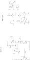
- Figure 1a shows an example of a known pulsed mode laser diode driver circuit (from the perspective of one half of a steered current unary pair, in other words the other half of the differential pair is not shown for simplicity).
- the laser diode 100 is coupled with its anode to the positive supply and the cathode to the current driver circuit.
- the circuit is provided with a clamp switch 113 in parallel with the laser diode 100.
- the driver circuit shown in Figure 1a shows a cascode arrangement with a cascode transistor 103 coupled to the laser diode and which is coupled to a current switch 111 for current steering and which is coupled to a current sink transistor 107 which is then coupled to the negative supply rail.
- the cascode transistor 103 is coupled by its gate to a mirrored cascode transistor 101, which is configured to mirror the current from the mirrored cascode transistor 101 to the cascode transistor 103 on a 1:N ratio.
- the current sink transistor 107 is also coupled by its gate to a mirrored current sink transistor 105, which is configured to mirror the current from the mirrored current sink transistor 105 to the current sink transistor 107 on a 1:N ratio also.
- a pulse of current defined by the current sink transistor 107 can be provided to the laser diode.
- FIG. 1b a further known pulse mode laser diode driver circuit is shown.
- the cascode transistors shown in Figure 1a are replaced with a pre-bias transistor pair 121, 123.
- the laser diode 120 is coupled with its anode to the pre-bias transistor pair 121, 123 and the cathode to the current sink transistor 129 which is mirrored by the mirrored current sink transistor 131.
- the circuit is provided with a clamp switch 127 in parallel with the laser diode 120.
- the driver circuit shown in Figure 1b shows the pre-bias transistor pair arrangement with a first pre-bias transistor 121 coupled to the laser diode and the positive supply rail and which is in parallel with a current switch 125.
- the first pre-bias transistor 121 is coupled by its gate to a mirrored pre-bias transistor 123 which mirrors the current from on defined ratio.
- the circuit is configured to be operated by sequentially closing the current switch 125 and then the clamp switch 127 to provide the laser diode with a pulse of current in order to produce the required output light intensity.
- Figure 1c shows a unary branch of a known sine wave mode circuit.
- the laser diode 140 is shown with an associated clamp switch 143 in parallel with the laser diode 140.
- the laser diode 140 is further coupled to the positive supply rail via an operational switch 141 which is configured to be closed while the circuit is operational.
- the driver circuit shown in Figure 1c further shows an arrangement similar to Figure 1a (but furthermore shows both switch paths for the unary DAC configuration) with a cascode transistor 147 coupled to the laser diode 140 and a current switch 153.
- the circuit further shows a current sink transistor 155 which is coupled to the current switch 153 and the negative supply rail.
- a further cascode transistor 145 and a further current switch 151 configured to provide the switch current path when the switch current path though the diode is not active.
- the cascode transistor 147 is common gate coupled to the further cascode transistor 145 and to a mirrored cascode transistor 149.
- the mirrored cascode transistor 149 is configured to mirror the current from the mirrored cascode transistor 149 to the cascode transistor 147 (and to the further cascode transistor 151) on a 1:N ratio.
- the current sink transistor 155 is also common gate coupled to a mirrored current sink transistor 157 which mirrors the current from the mirrored current sink transistor 157 to the current sink transistor 155 on a 1:N ratio.
- An arbitrary wave may be generated by combining several of the driver circuits in parallel and by operating the switches 151 and 153 to selectively change the sink current experienced by the diode 140.
- the circuits such as shown in Figure 1a and 1c by implementing a cascode arrangement in order to control Vdrain bias variation, have a switch rise and fall time which is defined by a parasitic gate capacitor C g and the bias current I bias of the current sink transistor. Furthermore the operating headroom of the cascode arrangement requires an operating voltage of Vov for both the cascode transistor. Vov, is the excess voltage of a MOSFET device (its Drain Source voltage) for which its mode of operation is in Saturation region.
- the concept as implemented in embodiments shown herein is to provide a laser diode driver implementation which displaces the cascode transistors but enables matching to be performed using a suitable closed loop feedback circuit and which controls the current sink transistors via a suitable low impedance output.
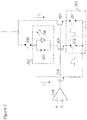
- Figure 2 shows an example implementation for a driver circuit which shows Z a part the laser diode driver according to the present invention.
- Figure 2 shows a modified version of the prior art laser diode driver circuit shown in Figure 1c .
- the operational switch 203 is coupled to the parallel arrangement of the laser diode 200 and clamp switch 201.
- the laser diode 200 may be coupled to a current sink transistor 209 which in turn is coupled to a first current steering switch 211 and which is in turn coupled to the negative supply rail.
- a current switch or shunt path shown by the arrow Is and which is arranged in parallel with the operating switch 203, laser diode 200 and current sink transistor 209 comprises a further current sink transistor 205 which is coupled to the positive supply rail and a second current steering switch 207, which is in turn coupled to the negative supply rail.
- the current sink transistor 209 and further current sink transistor 205 are gate coupled to a feedback transistor 213 which is configured to pass a feedback current If.
- the feedback transistor 213, the current sink transistor 209 and the further current sink transistor 205 are furthermore driven or coupled to the low impedance output of an operational amplifier 215.
- the operational amplifier 215 is configured to receive at a positive input a feedback voltage V f and further configured to receive at the negative input a reference voltage Vr.
- Such a MOSFET may present both reduction in switching gate capacitance and can be driven at native logic level (e.g. 1.1V, hence the ease of using standard logic cells as pre-drivers), also doing away with the need for level shifting, which impedes frequency of switching.
- native logic level e.g. 1.1V
- An additional advantage of such a circuit is that the switching can be filtered via a separate supply voltage (coupled to the feedback current supply) which can reduce fluctuations on the positive supply rail for the laser diode.
- the removal of the cascode transistor improves the operating headroom for the circuit.
- the transistors should be operated in saturation modes.
- the feedback loop attempts to simulate the operation of the laser diode for the current value driving the laser diode.
- GaAs Gallium Arsenide
- Vf forward biased voltage
- Si silicon diode drop
- the laser diode e.g. a VCSEL
- the laser diode is to be operated within the linear region of operation. This occurs when the diode is operated in the linear optical power output region above the pre-bias knee region at Ith, where it bounds the extinction of optical output power.
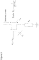
- the optical power against current curve is intrinsic to the device structure , it may be modelled by the mesa resistance R s which comprises the resistances from the P and N-Type distributed Bragg Reflector Mirrors, the sheet resistance from the n-contact layer and the P- and N- contacts and aperture of lasing window.
- the feedback loop may model the current required for the laser diode to generate a light intensity value by using a resistor value Rs.
- Figure 4a shows circuitry 400 comprising a modelled voltage forward based voltage generator 430 comprising a pair of forward biased diodes 405 and 407 in series between the positive supply rail and the regulator input.
- the circuity may additionally include resistors 415 and 417 between the positive supply rail and diodes 430.
- Figure 4a shows the anode of the diode 407 which is driven by an output voltage from a digital-to-analogue (DAC) converter 420.
- the DAC 420 can receive a digital input value which then outputs a suitable current output I DAC which impacts on the reference voltage input to the negative input of the operational amplifier 215.
- the feedback voltage generator part of the circuitry 400 comprises a further modelled voltage forward based voltage generator comprising a further pair of forward biased diodes 401 and 403 in series between the positive supply rail and the feedback input (the positive input of the operational amplifier 215).
- the feedback input is further coupled to a 'golden' resistor 409 which is configured to simulate the voltage drop caused by the linear response of the laser diode (R s ).
- the 'golden' resistor 409 is then coupled to the drain of the feedback transistor 213.
- the output of the operational amplifier 215 is coupled to the negative supply rail by a decoupling capacitor 413.
- a scaled equivalent to the peak DC level of the lasing current can be generated or 'programmed' by using a current DAC.
- This circuit thus generates a set point voltage using the two forward biased Si diodes, for which the Operational Amplifier then generates the regulate voltage (V REG ) and which is output and common gated to the elements such as shown in Figure 2 and furthermore with then used by the feedback loop by a referencing or 'golden unit' element.
- the 'golden' unit, which in Figure 4a is shown as the resistor 409 generates a model drain-source current (I DS ) and which is a ratio of the desired (or programmed) current (e.g. in this example a ratio of 1:1).
- the peak lasing current (or Full Scale, FS) is amplified by gains obtained by the open-loop current mirroring ratio of the golden unit to the summed unit elements that make up the unary DAC.
- the use of the feedback/tracking mechanism may in some embodiments be configured to be adjustable, for example by trimming the 'golden' resistor value for correction.
- FIG. 4b Another example, not falling under the scope of the present invention, of a circuit 450 for the generation of the reference and feedback voltage values which may be input to the operational amplifier 215 are shown in Figure 4b .
- This example circuit is similar to the circuit shown in figure 4a and like reference numerals refer to like circuit components.
- the circuit additionally includes a pair of resistors 415, 417. Resistor 415 is connected in series between the positive supply rail and the diodes 401, 403. Resistor 417 is connected between the positive supply rail and the regulator input. Resistor 417 may also be connected to the IDAC.
- the laser diode circuit in this example comprises the regulation voltage generator 400 which comprises a modelled voltage forward based voltage generator 430 comprising a pair of forward biased diodes 405 and 407 in series between the positive supply rail and the regulator input, the anode of the diode 407 which is driven by an output voltage from a digital-to-analogue (DAC) converter 420, a further modelled voltage forward based voltage generator comprising a further pair of forward biased diodes 401 and 403 in series between the positive supply rail and the feedback input (the positive input of the operational amplifier 215).
- DAC digital-to-analogue
- the feedback input is further coupled to a 'golden' element in the form of resistor 409 which is configured to simulate the voltage drop caused by the linear response of the laser diode (Rs) and the transistor 547 in parallel with the resistor which may simulate the non-linear voltage drop of the laser diode when not in the linear response region.
- the 'golden' element resistor 409 is then coupled to the drain of the feedback transistor 213.
- the circuit is shown further comprising a further transistor 534 coupled between the source of the feedback transistor 213 and the negative supply rail which simulates the effect of the current steering switches.
- the current driver is further shown with the current steering switches 211 and 207 as shown in Figure 2 implemented as transistors 521 and 523 which are driven via pre-drivers and which receive inputs from a decoder 535 which receives the digital to analogue converter input and switches between the diode and shunt current switch paths.
- a pre-bias module which comprises transistors 525, 527 and 529.
- the clamp switch 201 is shown implemented as a switch input which is coupled to the gate of an nmos transistor 511 and to the input of an inverter 513, the output of which is further coupled to the gate of a pmos transistor 515, where the nmos and pmos transistors are coupled in parallel with the laser diode 200.
- the operational switch 203 is shown implemented as a transistor 507 coupled between the positive supply rail and the laser diode 200.
- a current monitor in the form of a voltage to current converter 509 is shown coupled to the laser diode and furthermore a current measurement may be provided by a transistor 541 gate coupled to the output of the operational amplifier and further enabled by a measurement selector transistor 537.
- circuit is shown with a clock/pulse snubber comprising complementary transistors 501 and 503 and capacitor 505.
Landscapes
- Physics & Mathematics (AREA)
- Condensed Matter Physics & Semiconductors (AREA)
- General Physics & Mathematics (AREA)
- Electromagnetism (AREA)
- Optics & Photonics (AREA)
- Semiconductor Lasers (AREA)
Claims (12)
- Treiberschaltung (400, 600) für eine Laserdiode (200), ausgelegt zum Durchleiten eines Stroms, wobei die Schaltung Folgendes umfasst:einen ersten Transistor (209), in Serie mit der Laserdiode geschaltet und ausgelegt zum Regeln des Stroms; undeinen Spannungsregler (215), ausgelegt zum Liefern einer Eingabe an ein Gate des ersten Transistors, um somit den Strom in Abhängigkeit von einem ersten Eingang und einem zweiten Eingang des Spannungsreglers zu regeln,dadurch gekennzeichnet, dass der zweite Eingang des Spannungsreglers durch einen Modellspannung-Vorwärtsvorspannung-Erzeuger (430) gespeist wird, wobei der Modellspannung-Vorwärtsvorspannung-Erzeuger (430) ein erstes Paar von vorwärts vorgespannten Dioden (401, 403), die in Serie zwischen eine positive Speisung (VDD) und den zweiten Eingang des Spannungsreglers geschaltet sind, umfasst,wobei das erste Paar von vorwärts vorgespannten Dioden (401, 403) ausgelegt ist zum Modellieren einer Stromantwort der Laserdiode, wobei der erste Transistor (209) an einen Rückkopplungstransistor (213) Gate-gekoppelt ist, undein Widerstand (409) zwischen den zweiten Eingang des Spannungsreglers und die Drain des Rückkopplungstransistors (213) geschaltet ist.
- Treiberschaltung nach Anspruch 1, wobei der Spannungsregler einen Operationsverstärker umfasst.
- Treiberschaltung nach Anspruch 2, wobei der erste Eingang des Operationsverstärkers ein invertierender Eingang ist und der zweite Eingang des Operationsverstärkers ein nicht-invertierender Eingang ist.
- Treiberschaltung nach einem vorhergehenden Anspruch, ferner umfassend:
einen Digital-Analog-Wandler (420), ausgelegt zum Ausgeben eines Analogsignals an den ersten Eingang des Spannungsreglers, wobei das Analogsignal auf einer digitalen Repräsentation eines Laserdiodenausgabepegels basiert. - Treiberschaltung nach einem vorhergehenden Anspruch, wobei die digitale Repräsentation eines Laserdiodenausgabepegels eine digitale Repräsentation umfasst von:einer Dauerstrich-Laserausgabe; undeiner Pulsmodus-Laserausgabe.
- Treiberschaltung nach einem vorhergehenden Anspruch, ferner umfassend:einen Nebenschlusspfad, parallel zu der Laserdiode angeordnet, wobei der Nebenschlusspfad einen zweiten Transistor (205) umfasst, der ausgelegt ist zum Regeln eines Stroms in dem Nebenschlusspfad in Abhängigkeit von einer durch den Spannungsregler gelieferten Eingabe; undeinen oder mehrere Schalter (207, 211), ausgelegt zum Umschalten eines Stromflusses zwischen der Laserdiode und dem Nebenschlusspfad.
- Treiberschaltung nach Anspruch 1, wobei der Modellspannung-Vorwärtsvorspannung-Erzeuger ein zweites Paar von vorwärts vorgespannten Dioden (405, 407), die in Serie zwischen die positive Speisung und den ersten Eingang des Spannungsreglers geschaltet sind, umfasst.
- Treiberschaltung nach einem vorhergehenden Anspruch, ferner umfassend:
einen Klemmschalter (201), zu der Laserdiode parallelgeschaltet. - Treiberschaltung nach einem vorhergehenden Anspruch, wobei die Laserdiode ausgelegt ist zum Betrieb innerhalb eines linearen Betriebsbereichs.
- Treiberschaltung nach einem vorhergehenden Anspruch, wobei die Laserdiode eine oberflächenemittierende Laserdiode mit vertikaler Kavität bzw. "vertical cavity surface emitting laser diode" ist.
- Treiberschaltung nach einem vorhergehenden Anspruch, ferner umfassend:eine positive Speiseleitung (VDD), verbunden mit der Anode der Laserdiode; undeine negative Speiseleitung, verbunden mit der Kathode der Laserdiode,wobei die positive Speiseleitung und der negative Speiseanschluss zum Liefern des Stroms ausgelegt sind.
- Verfahren zum Betreiben einer Treiberschaltung (400, 600) für eine Laserdiode (200), ausgelegt zum Durchleiten eines Stroms, wobei das Verfahren Folgendes umfasst:Regeln des Stroms durch einen ersten Transistor (209), der in Serie mit der Laserdiode geschaltet ist; undLiefern einer Eingabe an ein Gate des ersten Transistors durch einen Spannungsregler (215), um somit den Strom in Abhängigkeit von einer ersten Eingabe und einer zweiten Eingabe an dem Spannungsregler zu regeln, dadurch gekennzeichnet, dass der zweite Eingang des Spannungsreglers durch einen Modellspannung-Vorwärtsvorspannung-Erzeuger (430) gespeist wird, wobei der Modellspannung-Vorwärtsvorspannung-Erzeuger (430) ein erstes Paar von vorwärts vorgespannten Dioden (401, 403), die in Serie zwischen eine positive Speisung (VDD) und den zweiten Eingang des Spannungsreglers geschaltet sind, umfasst,wobei das erste Paar von vorwärts vorgespannten Dioden (401, 403) ausgelegt ist zum Modellieren einer Stromantwort der Laserdiode und zum Simulieren des Spannungsabfalls, der durch die lineare Antwort der Laserdiode verursacht wird, durch einen Widerstand (409), der zwischen den zweiten Eingang des Spannungsreglers und die Drain eines Rückkopplungstransistors (213) geschaltet ist,wobei der Rückkopplungstransistor (213) an den ersten Transistor (209) Gate-gekoppelt ist.
Priority Applications (2)
| Application Number | Priority Date | Filing Date | Title |
|---|---|---|---|
| EP16189306.0A EP3297105B1 (de) | 2016-09-16 | 2016-09-16 | Treiberschlatung für eine laserdiode |
| US15/476,108 US10074961B2 (en) | 2016-09-16 | 2017-03-31 | Laser driver circuit and method of operating thereof |
Applications Claiming Priority (1)
| Application Number | Priority Date | Filing Date | Title |
|---|---|---|---|
| EP16189306.0A EP3297105B1 (de) | 2016-09-16 | 2016-09-16 | Treiberschlatung für eine laserdiode |
Publications (2)
| Publication Number | Publication Date |
|---|---|
| EP3297105A1 EP3297105A1 (de) | 2018-03-21 |
| EP3297105B1 true EP3297105B1 (de) | 2021-05-12 |
Family
ID=56979382
Family Applications (1)
| Application Number | Title | Priority Date | Filing Date |
|---|---|---|---|
| EP16189306.0A Active EP3297105B1 (de) | 2016-09-16 | 2016-09-16 | Treiberschlatung für eine laserdiode |
Country Status (2)
| Country | Link |
|---|---|
| US (1) | US10074961B2 (de) |
| EP (1) | EP3297105B1 (de) |
Families Citing this family (9)
| Publication number | Priority date | Publication date | Assignee | Title |
|---|---|---|---|---|
| JP7063651B2 (ja) * | 2018-02-19 | 2022-05-09 | エイブリック株式会社 | 信号検出回路及び信号検出方法 |
| EP3588703A1 (de) * | 2018-06-21 | 2020-01-01 | STMicroelectronics (Research & Development) Limited | Stromansteuerungsvorrichtung für eine laserdiode |
| US11996675B2 (en) | 2018-07-10 | 2024-05-28 | Sony Semiconductor Solutions Corporation | Laser drive circuit and sensor apparatus |
| CN111065187B (zh) * | 2018-10-17 | 2022-04-26 | 戴洛格半导体(英国)有限公司 | 电流调节器 |
| JP2020088020A (ja) * | 2018-11-16 | 2020-06-04 | ソニーセミコンダクタソリューションズ株式会社 | 検出回路、駆動回路および発光装置 |
| CN115443588B (zh) * | 2020-04-24 | 2025-03-07 | 华为技术有限公司 | 激光驱动器 |
| FR3119250A1 (fr) * | 2021-01-22 | 2022-07-29 | Stmicroelectronics (Grenoble 2) Sas | Pilote côté bas pour diode laser |
| CN114024604A (zh) * | 2021-12-07 | 2022-02-08 | 罗森伯格技术有限公司 | 光模块 |
| US20230318711A1 (en) * | 2022-04-05 | 2023-10-05 | Fathom Radiant, PBC | Optical Transceiver Methods and Apparatus for Integrated Optical Links |
Family Cites Families (12)
| Publication number | Priority date | Publication date | Assignee | Title |
|---|---|---|---|---|
| US5123023A (en) * | 1990-11-21 | 1992-06-16 | Polaroid Corporation | Laser driver with plural feedback loops |
| US5936986A (en) | 1996-07-30 | 1999-08-10 | Bayer Corporation | Methods and apparatus for driving a laser diode |
| JP3315892B2 (ja) * | 1997-04-24 | 2002-08-19 | 沖電気工業株式会社 | レーザーモジュールの制御回路 |
| WO2001003350A1 (en) * | 1999-07-01 | 2001-01-11 | Fujitsu Limited | Wdm optical transmitter |
| DE69942843D1 (de) * | 1999-08-03 | 2010-11-18 | Fujitsu Ltd | Schaltung zum steuern eines halbleiterlasers und steuerungsverfahren |
| US6711189B1 (en) * | 2000-02-04 | 2004-03-23 | Stratos Lightwave, Inc. | Automatic power control and laser slope efficiency normalizing circuit |
| US6917639B2 (en) | 2001-08-09 | 2005-07-12 | Ricoh Company, Ltd. | Laser driver circuit |
| JP2006100414A (ja) * | 2004-09-28 | 2006-04-13 | Sumitomo Electric Ind Ltd | 光送信器 |
| US7792166B2 (en) | 2005-06-24 | 2010-09-07 | Lockheed Martin Corporation | Apparatus and method for driving laser diodes |
| JP5092318B2 (ja) * | 2006-08-30 | 2012-12-05 | 日本電気株式会社 | 光送信器、その動作制御方法及びプログラム |
| US8401404B2 (en) | 2009-06-22 | 2013-03-19 | Stmicroelectronics S.R.L. | Optical receiver |
| US9972969B2 (en) * | 2013-02-28 | 2018-05-15 | Lawrence Livermore National Security, Llc | Compact high current, high efficiency laser diode driver |
-
2016
- 2016-09-16 EP EP16189306.0A patent/EP3297105B1/de active Active
-
2017
- 2017-03-31 US US15/476,108 patent/US10074961B2/en active Active
Non-Patent Citations (1)
| Title |
|---|
| None * |
Also Published As
| Publication number | Publication date |
|---|---|
| US10074961B2 (en) | 2018-09-11 |
| EP3297105A1 (de) | 2018-03-21 |
| US20180083419A1 (en) | 2018-03-22 |
Similar Documents
| Publication | Publication Date | Title |
|---|---|---|
| US10074961B2 (en) | Laser driver circuit and method of operating thereof | |
| EP0525819A1 (de) | Impulsverstärker für eine Halbleiterlasersteuerungsvorrichtung | |
| CN101326692B (zh) | 光发送电路 | |
| CN108711735B (zh) | 用于直调激光驱动器的温度补偿电路 | |
| JP2001326569A (ja) | Led駆動回路及び光送信モジュール | |
| JP6576306B2 (ja) | 電圧電流変換回路および負荷駆動回路 | |
| US9030263B2 (en) | Transimpedance amplifier (TIA) circuit and method | |
| DK0511354T3 (da) | Drivkredsløb til lasere | |
| JP4566692B2 (ja) | 発光ダイオード駆動装置及びそれを備えた光伝送装置 | |
| US8125273B2 (en) | Apparatus and method for driving an LED | |
| JP2004328640A (ja) | バイアス電流生成回路、レーザダイオード駆動回路及び光通信用送信器 | |
| CN114185052B (zh) | 激光发射驱动电路及激光雷达 | |
| US20170012406A1 (en) | Laser driver with maintaining average optical power constant | |
| KR20230166898A (ko) | 전류-제어식 세분화된 레이저 구동기 | |
| JP7283063B2 (ja) | 増幅回路 | |
| US20070153849A1 (en) | Adaptive laser diode driver and method | |
| JP5003586B2 (ja) | 半導体レーザ駆動回路 | |
| US7141936B2 (en) | Driving circuit for light emitting diode | |
| US9570917B2 (en) | Light emitting element drive circuit | |
| CN110120627B (zh) | 发光元件驱动电路 | |
| US9641170B2 (en) | Pass device with boost voltage regulation and current gain for VCSEL driving applications | |
| US7280574B1 (en) | Circuit for driving a laser diode and method | |
| JP6922505B2 (ja) | 半導体レーザ駆動回路 | |
| JP3593623B2 (ja) | 発光素子駆動回路 | |
| KR20100021648A (ko) | 광 송신기 |
Legal Events
| Date | Code | Title | Description |
|---|---|---|---|
| PUAI | Public reference made under article 153(3) epc to a published international application that has entered the european phase |
Free format text: ORIGINAL CODE: 0009012 |
|
| STAA | Information on the status of an ep patent application or granted ep patent |
Free format text: STATUS: THE APPLICATION HAS BEEN PUBLISHED |
|
| AK | Designated contracting states |
Kind code of ref document: A1 Designated state(s): AL AT BE BG CH CY CZ DE DK EE ES FI FR GB GR HR HU IE IS IT LI LT LU LV MC MK MT NL NO PL PT RO RS SE SI SK SM TR |
|
| AX | Request for extension of the european patent |
Extension state: BA ME |
|
| STAA | Information on the status of an ep patent application or granted ep patent |
Free format text: STATUS: REQUEST FOR EXAMINATION WAS MADE |
|
| 17P | Request for examination filed |
Effective date: 20180328 |
|
| RBV | Designated contracting states (corrected) |
Designated state(s): AL AT BE BG CH CY CZ DE DK EE ES FI FR GB GR HR HU IE IS IT LI LT LU LV MC MK MT NL NO PL PT RO RS SE SI SK SM TR |
|
| STAA | Information on the status of an ep patent application or granted ep patent |
Free format text: STATUS: EXAMINATION IS IN PROGRESS |
|
| 17Q | First examination report despatched |
Effective date: 20190909 |
|
| GRAP | Despatch of communication of intention to grant a patent |
Free format text: ORIGINAL CODE: EPIDOSNIGR1 |
|
| STAA | Information on the status of an ep patent application or granted ep patent |
Free format text: STATUS: GRANT OF PATENT IS INTENDED |
|
| RIC1 | Information provided on ipc code assigned before grant |
Ipc: H01S 5/062 20060101ALI20201103BHEP Ipc: H01S 5/042 20060101AFI20201103BHEP Ipc: H05B 33/08 20200101ALI20201103BHEP Ipc: H05B 45/48 20200101ALI20201103BHEP Ipc: H01S 5/0683 20060101ALN20201103BHEP |
|
| INTG | Intention to grant announced |
Effective date: 20201127 |
|
| RIC1 | Information provided on ipc code assigned before grant |
Ipc: H01S 5/042 20060101AFI20201117BHEP Ipc: H05B 33/08 20200101ALI20201117BHEP Ipc: H01S 5/062 20060101ALI20201117BHEP Ipc: H05B 45/48 20200101ALI20201117BHEP Ipc: H01S 5/0683 20060101ALN20201117BHEP |
|
| GRAS | Grant fee paid |
Free format text: ORIGINAL CODE: EPIDOSNIGR3 |
|
| GRAA | (expected) grant |
Free format text: ORIGINAL CODE: 0009210 |
|
| STAA | Information on the status of an ep patent application or granted ep patent |
Free format text: STATUS: THE PATENT HAS BEEN GRANTED |
|
| AK | Designated contracting states |
Kind code of ref document: B1 Designated state(s): AL AT BE BG CH CY CZ DE DK EE ES FI FR GB GR HR HU IE IS IT LI LT LU LV MC MK MT NL NO PL PT RO RS SE SI SK SM TR |
|
| REG | Reference to a national code |
Ref country code: GB Ref legal event code: FG4D |
|
| REG | Reference to a national code |
Ref country code: CH Ref legal event code: EP |
|
| REG | Reference to a national code |
Ref country code: DE Ref legal event code: R096 Ref document number: 602016057693 Country of ref document: DE |
|
| REG | Reference to a national code |
Ref country code: IE Ref legal event code: FG4D |
|
| REG | Reference to a national code |
Ref country code: AT Ref legal event code: REF Ref document number: 1392811 Country of ref document: AT Kind code of ref document: T Effective date: 20210615 |
|
| REG | Reference to a national code |
Ref country code: LT Ref legal event code: MG9D |
|
| REG | Reference to a national code |
Ref country code: AT Ref legal event code: MK05 Ref document number: 1392811 Country of ref document: AT Kind code of ref document: T Effective date: 20210512 |
|
| REG | Reference to a national code |
Ref country code: NL Ref legal event code: MP Effective date: 20210512 |
|
| PG25 | Lapsed in a contracting state [announced via postgrant information from national office to epo] |
Ref country code: FI Free format text: LAPSE BECAUSE OF FAILURE TO SUBMIT A TRANSLATION OF THE DESCRIPTION OR TO PAY THE FEE WITHIN THE PRESCRIBED TIME-LIMIT Effective date: 20210512 Ref country code: LT Free format text: LAPSE BECAUSE OF FAILURE TO SUBMIT A TRANSLATION OF THE DESCRIPTION OR TO PAY THE FEE WITHIN THE PRESCRIBED TIME-LIMIT Effective date: 20210512 Ref country code: HR Free format text: LAPSE BECAUSE OF FAILURE TO SUBMIT A TRANSLATION OF THE DESCRIPTION OR TO PAY THE FEE WITHIN THE PRESCRIBED TIME-LIMIT Effective date: 20210512 Ref country code: AT Free format text: LAPSE BECAUSE OF FAILURE TO SUBMIT A TRANSLATION OF THE DESCRIPTION OR TO PAY THE FEE WITHIN THE PRESCRIBED TIME-LIMIT Effective date: 20210512 Ref country code: BG Free format text: LAPSE BECAUSE OF FAILURE TO SUBMIT A TRANSLATION OF THE DESCRIPTION OR TO PAY THE FEE WITHIN THE PRESCRIBED TIME-LIMIT Effective date: 20210812 |
|
| PG25 | Lapsed in a contracting state [announced via postgrant information from national office to epo] |
Ref country code: GR Free format text: LAPSE BECAUSE OF FAILURE TO SUBMIT A TRANSLATION OF THE DESCRIPTION OR TO PAY THE FEE WITHIN THE PRESCRIBED TIME-LIMIT Effective date: 20210813 Ref country code: LV Free format text: LAPSE BECAUSE OF FAILURE TO SUBMIT A TRANSLATION OF THE DESCRIPTION OR TO PAY THE FEE WITHIN THE PRESCRIBED TIME-LIMIT Effective date: 20210512 Ref country code: IS Free format text: LAPSE BECAUSE OF FAILURE TO SUBMIT A TRANSLATION OF THE DESCRIPTION OR TO PAY THE FEE WITHIN THE PRESCRIBED TIME-LIMIT Effective date: 20210912 Ref country code: PL Free format text: LAPSE BECAUSE OF FAILURE TO SUBMIT A TRANSLATION OF THE DESCRIPTION OR TO PAY THE FEE WITHIN THE PRESCRIBED TIME-LIMIT Effective date: 20210512 Ref country code: NO Free format text: LAPSE BECAUSE OF FAILURE TO SUBMIT A TRANSLATION OF THE DESCRIPTION OR TO PAY THE FEE WITHIN THE PRESCRIBED TIME-LIMIT Effective date: 20210812 Ref country code: PT Free format text: LAPSE BECAUSE OF FAILURE TO SUBMIT A TRANSLATION OF THE DESCRIPTION OR TO PAY THE FEE WITHIN THE PRESCRIBED TIME-LIMIT Effective date: 20210913 Ref country code: SE Free format text: LAPSE BECAUSE OF FAILURE TO SUBMIT A TRANSLATION OF THE DESCRIPTION OR TO PAY THE FEE WITHIN THE PRESCRIBED TIME-LIMIT Effective date: 20210512 Ref country code: RS Free format text: LAPSE BECAUSE OF FAILURE TO SUBMIT A TRANSLATION OF THE DESCRIPTION OR TO PAY THE FEE WITHIN THE PRESCRIBED TIME-LIMIT Effective date: 20210512 |
|
| PG25 | Lapsed in a contracting state [announced via postgrant information from national office to epo] |
Ref country code: NL Free format text: LAPSE BECAUSE OF FAILURE TO SUBMIT A TRANSLATION OF THE DESCRIPTION OR TO PAY THE FEE WITHIN THE PRESCRIBED TIME-LIMIT Effective date: 20210512 |
|
| PG25 | Lapsed in a contracting state [announced via postgrant information from national office to epo] |
Ref country code: SM Free format text: LAPSE BECAUSE OF FAILURE TO SUBMIT A TRANSLATION OF THE DESCRIPTION OR TO PAY THE FEE WITHIN THE PRESCRIBED TIME-LIMIT Effective date: 20210512 Ref country code: SK Free format text: LAPSE BECAUSE OF FAILURE TO SUBMIT A TRANSLATION OF THE DESCRIPTION OR TO PAY THE FEE WITHIN THE PRESCRIBED TIME-LIMIT Effective date: 20210512 Ref country code: DK Free format text: LAPSE BECAUSE OF FAILURE TO SUBMIT A TRANSLATION OF THE DESCRIPTION OR TO PAY THE FEE WITHIN THE PRESCRIBED TIME-LIMIT Effective date: 20210512 Ref country code: EE Free format text: LAPSE BECAUSE OF FAILURE TO SUBMIT A TRANSLATION OF THE DESCRIPTION OR TO PAY THE FEE WITHIN THE PRESCRIBED TIME-LIMIT Effective date: 20210512 Ref country code: CZ Free format text: LAPSE BECAUSE OF FAILURE TO SUBMIT A TRANSLATION OF THE DESCRIPTION OR TO PAY THE FEE WITHIN THE PRESCRIBED TIME-LIMIT Effective date: 20210512 Ref country code: RO Free format text: LAPSE BECAUSE OF FAILURE TO SUBMIT A TRANSLATION OF THE DESCRIPTION OR TO PAY THE FEE WITHIN THE PRESCRIBED TIME-LIMIT Effective date: 20210512 Ref country code: ES Free format text: LAPSE BECAUSE OF FAILURE TO SUBMIT A TRANSLATION OF THE DESCRIPTION OR TO PAY THE FEE WITHIN THE PRESCRIBED TIME-LIMIT Effective date: 20210512 |
|
| REG | Reference to a national code |
Ref country code: DE Ref legal event code: R097 Ref document number: 602016057693 Country of ref document: DE |
|
| PLBE | No opposition filed within time limit |
Free format text: ORIGINAL CODE: 0009261 |
|
| STAA | Information on the status of an ep patent application or granted ep patent |
Free format text: STATUS: NO OPPOSITION FILED WITHIN TIME LIMIT |
|
| 26N | No opposition filed |
Effective date: 20220215 |
|
| REG | Reference to a national code |
Ref country code: CH Ref legal event code: PL |
|
| REG | Reference to a national code |
Ref country code: BE Ref legal event code: MM Effective date: 20210930 |
|
| GBPC | Gb: european patent ceased through non-payment of renewal fee |
Effective date: 20210916 |
|
| PG25 | Lapsed in a contracting state [announced via postgrant information from national office to epo] |
Ref country code: IS Free format text: LAPSE BECAUSE OF FAILURE TO SUBMIT A TRANSLATION OF THE DESCRIPTION OR TO PAY THE FEE WITHIN THE PRESCRIBED TIME-LIMIT Effective date: 20210912 Ref country code: MC Free format text: LAPSE BECAUSE OF FAILURE TO SUBMIT A TRANSLATION OF THE DESCRIPTION OR TO PAY THE FEE WITHIN THE PRESCRIBED TIME-LIMIT Effective date: 20210512 Ref country code: AL Free format text: LAPSE BECAUSE OF FAILURE TO SUBMIT A TRANSLATION OF THE DESCRIPTION OR TO PAY THE FEE WITHIN THE PRESCRIBED TIME-LIMIT Effective date: 20210512 |
|
| PG25 | Lapsed in a contracting state [announced via postgrant information from national office to epo] |
Ref country code: LU Free format text: LAPSE BECAUSE OF NON-PAYMENT OF DUE FEES Effective date: 20210916 Ref country code: IT Free format text: LAPSE BECAUSE OF FAILURE TO SUBMIT A TRANSLATION OF THE DESCRIPTION OR TO PAY THE FEE WITHIN THE PRESCRIBED TIME-LIMIT Effective date: 20210512 Ref country code: IE Free format text: LAPSE BECAUSE OF NON-PAYMENT OF DUE FEES Effective date: 20210916 Ref country code: GB Free format text: LAPSE BECAUSE OF NON-PAYMENT OF DUE FEES Effective date: 20210916 Ref country code: FR Free format text: LAPSE BECAUSE OF NON-PAYMENT OF DUE FEES Effective date: 20210930 Ref country code: BE Free format text: LAPSE BECAUSE OF NON-PAYMENT OF DUE FEES Effective date: 20210930 |
|
| PG25 | Lapsed in a contracting state [announced via postgrant information from national office to epo] |
Ref country code: LI Free format text: LAPSE BECAUSE OF NON-PAYMENT OF DUE FEES Effective date: 20210930 Ref country code: CH Free format text: LAPSE BECAUSE OF NON-PAYMENT OF DUE FEES Effective date: 20210930 |
|
| PG25 | Lapsed in a contracting state [announced via postgrant information from national office to epo] |
Ref country code: HU Free format text: LAPSE BECAUSE OF FAILURE TO SUBMIT A TRANSLATION OF THE DESCRIPTION OR TO PAY THE FEE WITHIN THE PRESCRIBED TIME-LIMIT; INVALID AB INITIO Effective date: 20160916 |
|
| PG25 | Lapsed in a contracting state [announced via postgrant information from national office to epo] |
Ref country code: CY Free format text: LAPSE BECAUSE OF FAILURE TO SUBMIT A TRANSLATION OF THE DESCRIPTION OR TO PAY THE FEE WITHIN THE PRESCRIBED TIME-LIMIT Effective date: 20210512 |
|
| PG25 | Lapsed in a contracting state [announced via postgrant information from national office to epo] |
Ref country code: MK Free format text: LAPSE BECAUSE OF FAILURE TO SUBMIT A TRANSLATION OF THE DESCRIPTION OR TO PAY THE FEE WITHIN THE PRESCRIBED TIME-LIMIT Effective date: 20210512 |
|
| PG25 | Lapsed in a contracting state [announced via postgrant information from national office to epo] |
Ref country code: MT Free format text: LAPSE BECAUSE OF FAILURE TO SUBMIT A TRANSLATION OF THE DESCRIPTION OR TO PAY THE FEE WITHIN THE PRESCRIBED TIME-LIMIT Effective date: 20210512 |
|
| PGFP | Annual fee paid to national office [announced via postgrant information from national office to epo] |
Ref country code: DE Payment date: 20250820 Year of fee payment: 10 |
|
| PG25 | Lapsed in a contracting state [announced via postgrant information from national office to epo] |
Ref country code: TR Free format text: LAPSE BECAUSE OF FAILURE TO SUBMIT A TRANSLATION OF THE DESCRIPTION OR TO PAY THE FEE WITHIN THE PRESCRIBED TIME-LIMIT Effective date: 20210512 |
|
| REG | Reference to a national code |
Ref country code: DE Ref legal event code: R082 Ref document number: 602016057693 Country of ref document: DE Representative=s name: WESTPHAL, MUSSGNUG & PARTNER PATENTANWAELTE MI, DE |