EP0525819A1 - Impulsverstärker für eine Halbleiterlasersteuerungsvorrichtung - Google Patents
Impulsverstärker für eine Halbleiterlasersteuerungsvorrichtung Download PDFInfo
- Publication number
- EP0525819A1 EP0525819A1 EP92113686A EP92113686A EP0525819A1 EP 0525819 A1 EP0525819 A1 EP 0525819A1 EP 92113686 A EP92113686 A EP 92113686A EP 92113686 A EP92113686 A EP 92113686A EP 0525819 A1 EP0525819 A1 EP 0525819A1
- Authority
- EP
- European Patent Office
- Prior art keywords
- pulse
- fet
- input
- voltage
- gate
- Prior art date
- Legal status (The legal status is an assumption and is not a legal conclusion. Google has not performed a legal analysis and makes no representation as to the accuracy of the status listed.)
- Pending
Links
Images


Classifications
-
- H—ELECTRICITY
- H01—ELECTRIC ELEMENTS
- H01S—DEVICES USING THE PROCESS OF LIGHT AMPLIFICATION BY STIMULATED EMISSION OF RADIATION [LASER] TO AMPLIFY OR GENERATE LIGHT; DEVICES USING STIMULATED EMISSION OF ELECTROMAGNETIC RADIATION IN WAVE RANGES OTHER THAN OPTICAL
- H01S5/00—Semiconductor lasers
- H01S5/06—Arrangements for controlling the laser output parameters, e.g. by operating on the active medium
- H01S5/062—Arrangements for controlling the laser output parameters, e.g. by operating on the active medium by varying the potential of the electrodes
- H01S5/06209—Arrangements for controlling the laser output parameters, e.g. by operating on the active medium by varying the potential of the electrodes in single-section lasers
- H01S5/06216—Pulse modulation or generation
-
- H—ELECTRICITY
- H01—ELECTRIC ELEMENTS
- H01S—DEVICES USING THE PROCESS OF LIGHT AMPLIFICATION BY STIMULATED EMISSION OF RADIATION [LASER] TO AMPLIFY OR GENERATE LIGHT; DEVICES USING STIMULATED EMISSION OF ELECTROMAGNETIC RADIATION IN WAVE RANGES OTHER THAN OPTICAL
- H01S5/00—Semiconductor lasers
- H01S5/06—Arrangements for controlling the laser output parameters, e.g. by operating on the active medium
- H01S5/068—Stabilisation of laser output parameters
- H01S5/0683—Stabilisation of laser output parameters by monitoring the optical output parameters
- H01S5/06835—Stabilising during pulse modulation or generation
-
- H—ELECTRICITY
- H03—ELECTRONIC CIRCUITRY
- H03K—PULSE TECHNIQUE
- H03K5/00—Manipulating of pulses not covered by one of the other main groups of this subclass
- H03K5/01—Shaping pulses
- H03K5/02—Shaping pulses by amplifying
- H03K5/023—Shaping pulses by amplifying using field effect transistors
-
- H—ELECTRICITY
- H03—ELECTRONIC CIRCUITRY
- H03K—PULSE TECHNIQUE
- H03K5/00—Manipulating of pulses not covered by one of the other main groups of this subclass
- H03K5/01—Shaping pulses
- H03K5/08—Shaping pulses by limiting; by thresholding; by slicing, i.e. combined limiting and thresholding
- H03K5/082—Shaping pulses by limiting; by thresholding; by slicing, i.e. combined limiting and thresholding with an adaptive threshold
- H03K5/086—Shaping pulses by limiting; by thresholding; by slicing, i.e. combined limiting and thresholding with an adaptive threshold generated by feedback
-
- H—ELECTRICITY
- H01—ELECTRIC ELEMENTS
- H01S—DEVICES USING THE PROCESS OF LIGHT AMPLIFICATION BY STIMULATED EMISSION OF RADIATION [LASER] TO AMPLIFY OR GENERATE LIGHT; DEVICES USING STIMULATED EMISSION OF ELECTROMAGNETIC RADIATION IN WAVE RANGES OTHER THAN OPTICAL
- H01S5/00—Semiconductor lasers
- H01S5/04—Processes or apparatus for excitation, e.g. pumping, e.g. by electron beams
- H01S5/042—Electrical excitation ; Circuits therefor
- H01S5/0428—Electrical excitation ; Circuits therefor for applying pulses to the laser
Definitions
- the present invention relates to a semiconductor laser driving device and a pulse amplifier suitable for use as a pulse current supply circuit in the semiconductor laser driving device.
- This pulse amplifier varies a pulse amplitude of an output pulse in response to a control signal.
- the semiconductor laser driving device is used for controlling an excitation of the semiconductor laser, such as a laser diode, used as a light source in an optical communication system.
- the optical communication system is suitable for a large capacity data transmission, in which the laser diode must be driven at an ultra high transmission rate (G bit/s order). Accordingly, the semiconductor laser driving device and the pulse amplifier used therein, which can operate at the ultra high transmission rate, are required.
- the semiconductor laser driving device in the prior art comprises a bias current supply circuit for supplying a bias current to the laser diode, a pulse current supply circuit for supplying a pulse current to the laser diode for exciting the laser diode to emit a light, and an automatic power control loop for controlling the magnitude of the base current and the pulse amplitude of the pulse current to maintain the output light of the laser diode at a constant power.
- the bias current and pulse current supply circuits are constituted by using, as active elements, bipolar transistors having almost the same characteristic.
- the transmission rate of the semiconductor laser driving device has an upper limit on the order of about 100s M bit/s and, therefore, the bipolar transistor can not be used for a semiconductor laser driving device operated at 1 G bit/s, which will become more necessary in the future.
- This limitation to the transmission rate is due to a physical characteristic of the bipolar transistor, and therefore, the transmission rate cannot be increased merely by changing a circuit constitution of the driving device.
- an FET Field Effect Transistor
- GaAs FET Field Effect Transistor
- a pulse amplifier for varying a pulse amplitude of an input pulse in response to a control signal, comprising first and second FET's connected in cascade, wherein: the first FET is constituted so that the input pulse is input to a gate electrode thereof and a gate-source voltage variable in response to the control signal is biased so that one of top side portion and base side portion of the input pulse is cut off at a pinchoff voltage thereof; and the second FET is constituted so that the input pulse output from the first FET is input to a gate electrode thereof and a gate-source voltage is biased so that the side portion of the input pulse which is not cut off is cut off at a pinchoff voltage thereof.
- FIG. 1 is a view showing an example of the semiconductor laser driving device of the prior art.
- a laser diode module comprising a laser diode LD which outputs a forward laser light into a optical fiber (not shown), and at the same time, a backward laser light as a monitoring light to be monitored, and an avalanche photodiode APD which receives the monitoring light and converts it into a monitoring; current l m ;
- 2 is a bias current supply circuit for supplying a DC bias current for the laser diode LD, which circuit comprises a bipolar transistor Q1 and a resistor R1;
- 3 is a pulse current supply circuit for supplying a pulse current for the laser diode LD in such a manner that the pulse current is superimposed on the bias current, which circuit comprises bipolar transistors Q2 to Q4 and a resistor R2;
- 4 is a low pass filter for extracting a low frequency component of data input pulse DT(in); 5 is a low pass filter for
- the pulse current supply circuit 3 receives the data input pulses DT(in) at the base of the transistor Q2 to supply a pulse current Ip correspondingto the input pulse DT(in) to the laser diode LD.
- a reversed input pulse DT(in) is input to a base of the transistor Q3.
- Figure 2 is a graph showing an operating characteristic of the laser diode, in which the abscissa denotes a driving current I d flowing through the laser diode LD and the ordinate denotes an output power L of the laser light emitted from the laser diode.
- the characteristic curves A, B, and C correspond to operating temperatures of 5 ° C, 25 °C, and 50 °C, respectively.
- the bias current I b is a DC current slightly lower than a threshold current l th of the laser diode LD.
- the pulse current Ip is superimposed on the bias current I b , whereby the pulselike laser light corresponding to the pulse current Ip is output from the laser diode LD.
- the automatic power control loop is provided for compensating this variation, by comparing the average value of the input pulses DT(in) output from the low pass filter 4 with the average value of the monitoring current l m output from the low pass filter 5 at the control circuit 6, then outputting the control voltage V a p c to make these average values coincide and thus control the bias current I b and the pulse current lp , thereby maintaining the output light at a constant value.
- the bias value I b is proportional to
- the feedback control is performed on the basis of the average values of the pulse train output from the low pass filters 4 and 5, because a feedback control by which a peak value of the light output pulse is maintained at a constant value by following up each of the input pulses DT(in) is difficult, due to the high transmission rate thereof.
- the monitoring light from the laser diode LD is detected by the photodiode APD, and a pulse amplitude of the pulse current supplied from the pulse current supply circuit 3 and the value of the DC bias current supplied from the bias current supply circuit are fedback in response to the detected value of the monitoring light, and thus an automatic power control of the output light is carried out to maintain a constant average value of the output light.
- the semiconductor laser driving device shown in Fig. 1 uses bipolar transistors as active elements in the bias current and pulse current supply circuits 2 and 3.
- the bipolar transistors are used because the differences between the base voltage and collector current characteristics of each device are small, and accordingly, in the automatic power control loop, the output of the control circuit 6 may be directly fedback to the transistors Q1 and Q4.
- the transmission rate is limited to, for example, an upper order of 100s Mb/S, which can not cope with a demand for a 1 Gb/s transmission rate, which demand will become greater in the future.
- Figure 3 is a view showing the semiconductor laser driving device as a relevant art of the present invention, in which high speed FET's capable of operating at a transmission rate of 1 to 2 Gb/s order, such as Gallium Arsenide FET's, are used as active elements in the bias current and pulse current supply circuits.
- This driving device is intended to further increase the transmission rate.
- parts bearing the same reference numerals as shown in Fig. 1 denote the same parts having the same function.
- a bias current supply circuit 7 comprises an FET Q5 with a gate to which the control voltage V a p c is input.
- a pulse current supply circuit 8 comprises a capacitor C2, an FET Q6 with a gate to which the input pulse DT(in) is input, and a low level clamping diode D1 through which the control voltage V a p c is applied to the gate of the FET Q6.
- gate-source voltages of the FET's Q5 and Q6 are varied according to the control voltage V a p c , and accordingly, the magnitude of the bias current I b and the pulse amplitude of the pulse current Ip are varied to perform an automatic power control.
- the supply circuit 8 supplies a pulse current Ip corresponding to an input pulse DT(in), the pulse current amplitute of which is varied in response to the control voltage V a p c , to the laser diode LD.
- Figure 4 is a graph showing a V GS -l D characteristic of the FET Q6, in which Vp o denotes a pinchoff voltage of the FET Q6.
- the gate-source voltage V GS of the FET Q6 is biased at V GS2 , which is higher than V GS1 , the portion of the input pulse DT(in) 2 cut off at the pinchoff voltage Vp o becomes greater than the cut off portion of the input pulse DT(in)i , and the residual part thereof is output as the pulse current Ip 2 having a pulse amplitude PA 2 greater than the pulse amplitude PA 1 . That is, PA 1 ⁇ PA 2 .
- the pulse amplitude of the pulse current Ip is varied in response to the control voltage V a p c , which varies the gate-source voltage V Gs of the FET Q6.
- the pulse width is defined as a width between mesial points of the pulse amplitude of the pulse.
- the pulse DT(in) has the trapezoidal waveform shown in Fig. 4 instead of a rectangular waveform, since a rise time and a fall time of the pulse cannot be ignored with respect to the pulse width.
- the pulse width of the pulse current Ip is varied according to the position at which the input pulse DT(in) is sliced by the pinchoff voltage Vp o , i.e., the magnitude of the control voltage V a p c .
- the pulse width of the pulse current Ip 1 becomes PW
- the pulse width of the pulse current Ip 2 becomes PW 2 , where PW 1 ⁇ PW 2 .
- the pulse width of the pulse current supplied to the laser diode LD may be varied, which will cause variations in a duty factor defined as a ratio of the pulse width to the pulse repetition frequency.
- a duty factor defined as a ratio of the pulse width to the pulse repetition frequency.
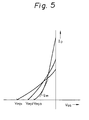
- FIG. 5 is a graph showing differences of the V GS -l D characteristics of the FET's.
- the V GS -l D characteristics of three FET's each having a different characteristic are denoted, respectively.
- the three FET's have pinchoff voltages Vp oi , Vp o2 , and Vp o3 , respectively.
- each slope of the characteristic curves i.e., mutual conductance gm, is different not only for each FET but also in accordance with the magnitude of the gate-source voltage V Gs .
- FIG. 6 is a view of an embodiment of the semiconductor laser driving device according to the present invention.
- a pulse current supply circuit 9 comprises two FET's Q7 and Q8 connected in cascade, and the control voltage V apc output from the power control circuit 6 is input to the bias current supply circuit 7 and the pulse current supply circuit 9 via compensating circuits 10 and 11 respectively.
- the compensating circuit 10 comprises an operational amplifier OP1, resistors R5 to R7, and a variable resistor VR1 for adjusting a gain.
- the circuit 10 is constituted so that an offset adjusting voltage V of1 can be applied to an inverting terminal of the operational amplifier OP1.
- the compensating circuit 11 comprises an operational amplifier OP2, resistors R8 to R10, and a variable resistor VR2, and is constituted so that an offset adjusting voltage V of2 can be applied to an inverting terminal of the operational amplifier OP2.
- the pulse current supply circuit 9 is constituted by two stage FET's Q7 and Q8 connected in cascade.
- the first stage FET Q7 receives at the gate thereof the data input pulse DT(in) through a capacitor C2, and at the same time, receives the control voltage V apc from the control circuit 6 through the compensating circuit 11 and a diode D2.
- a constant voltage power supply (-V) is connected to the source of the FET Q7. Therefore, the gate-source voltage V GS1 of the FET Q7 can be varied in response to the control voltage V a p c , which causes the variations of the pulse amplitude of the pulse current Ip.
- the diode D2 is a high level side clamping diode for the input pulse DT(in).
- the FET Q7 outputs an output pulse signal from the drain thereof grounded through the resistor R4 to the gate of the next stage FET Q8 through a capacitor C3.
- the gate of the FET Q8 is connected to the constant voltage power source (-V c ) through a low level side clamping diode D3, and the source thereof is connected to the constant voltage power source (-V). Accordingly, the gate-source voltage V GS2 of the FET Q8 is constant.
- the drain of the FET Q8 is connected to the laser diode LD, and thus the output pulse current Ip is supplied to the laser diode LD.
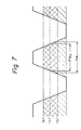
- Figure 7 is a drawing for explaining a principle of the operation of the circuit 9.
- a principle of the operation of the pulse current supply circuit 9 will be explained with reference to Fig. 7.
- Figure 7 shows pulse waveform having a pulse width PW o corresponding to the width between mesial points between the pulse top and pulse base, the duty factor of which is 50%.
- the pulse waveform is cut off along the broken line (a) by the pinch-off voltage Vp o1 of the first stage FET Q7 to obtain the waveform portion below the broken line (a) (the portion shown by oblique lines).
- the pulse width PW 1 of the obtained pulse waveform i.e., the width between mesial points between the pulse top and the pulse base, becomes greater than the pulse width PWo. Accordingly, the duty factor thereof becomes greater than 50%.
- the obtained pulse waveform (the portion shown by oblique lines) is then cut off along one-dot chain line (b) by the pinch-off voltage Vp o2 of the FET Q8 to obtain the portion above the one-dot chain line (b) (the portion of shown cross-hatching lines).
- the obtained pulse waveform has a pulse width very close to the pulse width PWo , and a duty factor of almost 50%.
- the original pulse waveform is sliced at the upper side portion and lower side portion with respect to the mesial point thereof, so that the pulse width and duty factor may be kept almost constant.
- Figure 8 is a graph of the l D -V GS characteristic of the FET Q7, in which input and output waveforms are denoted.
- Figure 9 is a graph of the l D -V GS characteristic of the FET Q8, in which input and output waveforms are also denoted.
- the input pulse DT(in) input to the FET Q7 is a negative logic level pulse and has a constant pulse width.
- the input pulse DT(in) 3 having a pulse base level of -V GS11 is cut off at the pinch-off voltage V PO1 to eliminate the pulse top side portion, i.e. logic "1" side portion, so that the output pulse current lp 3 has a pulse amplitude PA 3 and a pulse width PW 3 .
- the output pulse current Ip 4 has a pulse amplitude PA 4 and a pulse width PW 4 , where PA 3 ⁇ PA 4 and PW 3 > PW 4 .
- the output pulse current lp 3 or Ip 4 of the FET Q7 is then converted into the output pulse voltage P 3 or P 4 to be input to the second stage FET Q8 respectively.
- the pulse base of the input pulse i.e., "0" level of the input pulse, is arranged at a constant voltage V Gsc .
- the input pulse P 3 or P 4 corresponding to the pulse current lp 3 or Ip 4 respectively is cut off at the same position of the pulse base side, to cut off the pulse base side portion thereof with respect to the mesial point of the original input data pulse DT(in) respectively, and then output as the output pulse current lp 3 or Ip 4 having the pulse amplitude PA 5 or PA 6 and pulse width PW 5 or PW 6 , respectively.
- the output pulse currents lp 3 or Ip 4 have almost the same pulse width PW 5 or PW 6 , but have a different pulse amplitude PA 5 or PA 6 varied according to the variation of the gate-source voltage V GS1 of the first stage FET Q7, respectively.
- the control for varying the pulse amplitude without varying the pulse width is realized.
- the gate-source voltage V GS1 of the first stage FET Q7 is variable, but the gate-source voltage V GS2 of the second stage FET Q8 is fixed. Nevertheless, to absorb a variation of the pinch-off voltage of the FET, it may be desirable to vary the gate-source voltage V GS2 of the FET Q8.
- each FET is compensated by adjusting the gains of the operational amplifiers OP1 and OP2 by means of the variable resistors VR1 and VR2, to vary the magnitudes of the control voltage V a p c supplied from the control circuit 6 to the pulse current and bias current supply circuits 7 and 9 respectively.
- compensation is made only for a deviation of the characteristic of the FET.
- the gains of the operational amplifiers OP1 and OP2 may be compensated by adjusting the gains of the operational amplifiers OP1 and OP2 by means of the variable resistors VR1 and VR2 and offset voltages V of1 and Vp f2 .
- the input pulse DT(in) input to the pulse current supply circuit 9 has a negative logic, but a positive logic input pulse also may be utilized.
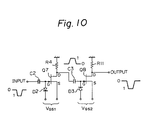
- Figure 10 shown a circuit diagram of a pulse amplifier, according to the present invention, which has a general configuration.
- the pulse amplifier used as the pulse current supply circuit 9 shown in Fig. 6 is used for another purpose, in general, the drain of the FET Q8 is grounded through the load resistor R11 instead of the laser diode LD.
Landscapes
- Physics & Mathematics (AREA)
- Condensed Matter Physics & Semiconductors (AREA)
- General Physics & Mathematics (AREA)
- Electromagnetism (AREA)
- Optics & Photonics (AREA)
- Nonlinear Science (AREA)
- Semiconductor Lasers (AREA)
Applications Claiming Priority (4)
| Application Number | Priority Date | Filing Date | Title |
|---|---|---|---|
| JP23463485A JPS6294994A (ja) | 1985-10-22 | 1985-10-22 | レ−ザダイオ−ド駆動回路 |
| JP234634/85 | 1985-10-22 | ||
| JP5946486A JPS62217712A (ja) | 1986-03-19 | 1986-03-19 | パルス増幅器 |
| JP59464/86 | 1986-03-19 |
Related Parent Applications (1)
| Application Number | Title | Priority Date | Filing Date |
|---|---|---|---|
| EP86114613.2 Division | 1986-10-22 |
Publications (1)
| Publication Number | Publication Date |
|---|---|
| EP0525819A1 true EP0525819A1 (de) | 1993-02-03 |
Family
ID=26400512
Family Applications (3)
| Application Number | Title | Priority Date | Filing Date |
|---|---|---|---|
| EP19920107690 Withdrawn EP0499293A3 (en) | 1985-10-22 | 1986-10-22 | A pulse amplifier suitable for use in a semiconductor laser driving device |
| EP92113686A Pending EP0525819A1 (de) | 1985-10-22 | 1986-10-22 | Impulsverstärker für eine Halbleiterlasersteuerungsvorrichtung |
| EP86114613A Withdrawn EP0220669A3 (de) | 1985-10-22 | 1986-10-22 | Halbleiterlaser-Steuerungsvorrichtung |
Family Applications Before (1)
| Application Number | Title | Priority Date | Filing Date |
|---|---|---|---|
| EP19920107690 Withdrawn EP0499293A3 (en) | 1985-10-22 | 1986-10-22 | A pulse amplifier suitable for use in a semiconductor laser driving device |
Family Applications After (1)
| Application Number | Title | Priority Date | Filing Date |
|---|---|---|---|
| EP86114613A Withdrawn EP0220669A3 (de) | 1985-10-22 | 1986-10-22 | Halbleiterlaser-Steuerungsvorrichtung |
Country Status (4)
| Country | Link |
|---|---|
| US (2) | US4803384A (de) |
| EP (3) | EP0499293A3 (de) |
| AU (2) | AU574587B2 (de) |
| NZ (1) | NZ218022A (de) |
Cited By (2)
| Publication number | Priority date | Publication date | Assignee | Title |
|---|---|---|---|---|
| FR3059439A1 (fr) * | 2016-11-30 | 2018-06-01 | Stmicroelectronics Sa | Generateur de signal d'horloge |
| US10312889B2 (en) | 2016-11-30 | 2019-06-04 | Stmicroelectronics Sa | Clock signal generator |
Families Citing this family (41)
| Publication number | Priority date | Publication date | Assignee | Title |
|---|---|---|---|---|
| DE3608930A1 (de) * | 1986-03-18 | 1987-09-24 | Standard Elektrik Lorenz Ag | Verfahren zur regelung der optischen leistung eines lasers und schaltung zur ausuebung des verfahrens |
| NL8602303A (nl) * | 1986-09-12 | 1988-04-05 | Philips Nv | Werkwijze voor het in pulsmode aansturen van een halfgeleiderlaser, aanstuurinrichting voor een halfgeleiderlaser en laserschrijfapparaat voorzien van een dergelijke aanstuurinrichting. |
| GB2208962B (en) * | 1987-08-19 | 1991-05-08 | Plessey Co Plc | Power supply |
| JPH07114349B2 (ja) * | 1988-12-28 | 1995-12-06 | 株式会社東芝 | デューティ制御回路装置 |
| JPH02228084A (ja) * | 1989-03-01 | 1990-09-11 | Fujitsu Ltd | 半導体レーザの駆動回路 |
| US5128950A (en) * | 1989-08-02 | 1992-07-07 | Hamamatsu Photonics K.K. | Low noise pulsed light source using laser diode |
| US5111065A (en) * | 1990-03-23 | 1992-05-05 | Massachusetts Institute Of Technology | Diode driver circuit utilizing discrete-value DC current source |
| US5121401A (en) * | 1990-05-03 | 1992-06-09 | Motorola, Inc. | Pulsed modulators utilizing transmission lines |
| US5316795A (en) * | 1990-05-24 | 1994-05-31 | Houston Advanced Research Center | Halogen-assisted chemical vapor deposition of diamond |
| US5071677A (en) * | 1990-05-24 | 1991-12-10 | Houston Advanced Research Center | Halogen-assisted chemical vapor deposition of diamond |
| US5179565A (en) * | 1990-06-07 | 1993-01-12 | Hamamatsu Photonics, K.K. | Low noise pulsed light source utilizing laser diode and voltage detector device utilizing same low noise pulsed light source |
| JP2525943B2 (ja) * | 1990-08-02 | 1996-08-21 | 富士通株式会社 | 光学記録再生装置のレ―ザダイオ―ド制御方式 |
| JPH04117834A (ja) * | 1990-09-07 | 1992-04-17 | Mitsubishi Electric Corp | デジタル伝送回路 |
| US5305338A (en) * | 1990-09-25 | 1994-04-19 | Mitsubishi Denki Kabushiki Kaisha | Switch device for laser |
| JPH04132428A (ja) * | 1990-09-25 | 1992-05-06 | Canon Inc | 光通信方式及びそこに用いられる受信装置 |
| JPH04206583A (ja) * | 1990-11-30 | 1992-07-28 | Fujitsu Ltd | 波長可変レーザの駆動装置 |
| US5309269A (en) * | 1991-04-04 | 1994-05-03 | Mitsubishi Denki Kabushiki Kaisha | Light transmitter |
| GB2258753B (en) * | 1991-08-15 | 1995-02-15 | Northern Telecom Ltd | Injection laser modulation |
| JPH0582876A (ja) * | 1991-09-18 | 1993-04-02 | Minolta Camera Co Ltd | レーザダイオードユニツトの駆動方法 |
| US5687001A (en) * | 1992-01-22 | 1997-11-11 | Dai Nippon Printing Co., Ltd. | Halftone image ion printer |
| JP3226624B2 (ja) * | 1992-09-24 | 2001-11-05 | 日本オプネクスト株式会社 | レーザダイオード駆動回路及び光伝送装置 |
| JPH0851318A (ja) * | 1994-08-08 | 1996-02-20 | Oki Electric Ind Co Ltd | 利得可変回路とその集積回路 |
| US5455837A (en) * | 1994-09-22 | 1995-10-03 | Coherent, Inc. | Flashlamp energy control circuit |
| JP2655508B2 (ja) * | 1995-03-07 | 1997-09-24 | 日本電気株式会社 | 光送信回路 |
| JPH0964441A (ja) * | 1995-08-23 | 1997-03-07 | Fujitsu Ltd | 発光素子駆動装置 |
| JP3784485B2 (ja) * | 1997-02-12 | 2006-06-14 | 富士通株式会社 | 出力パルス幅制御システム |
| US5987045A (en) * | 1997-04-02 | 1999-11-16 | The United States Of America As Represented By The Secretary Of The Navy | High power narrow pulse laser diode circuit |
| US20020097468A1 (en) * | 2001-01-24 | 2002-07-25 | Fsona Communications Corporation | Laser communication system |
| US6587490B2 (en) * | 2001-10-02 | 2003-07-01 | Analog Modules, Inc | Low-noise current source driver for laser diodes |
| EP1611572A1 (de) * | 2003-03-27 | 2006-01-04 | Koninklijke Philips Electronics N.V. | Strahlungsquellenansteuereinrichtung und verfahren zum ansteuern einer strahlungsquelle |
| JP4570862B2 (ja) * | 2003-10-27 | 2010-10-27 | 株式会社リコー | 半導体レーザ駆動回路 |
| US7019565B2 (en) * | 2003-11-04 | 2006-03-28 | Broadcom Corporation | Methods and systems for fully differential frequency doubling |
| JP2005317666A (ja) * | 2004-04-27 | 2005-11-10 | Sumitomo Electric Ind Ltd | レーザ駆動回路 |
| DE102004058595B4 (de) * | 2004-11-26 | 2009-04-02 | Atmel Germany Gmbh | Treiberschaltung und Verfahren zur Kompensation von Offsetströmen in einer Treiberschaltung |
| TWI314328B (en) * | 2005-02-25 | 2009-09-01 | Delta Electronics Inc | System of adjusting optical character by trimmable resistor and adjusting method thereof |
| US7839906B1 (en) * | 2006-06-07 | 2010-11-23 | Marvell International Ltd. | Laser power control in an optical disc drive |
| JP5027680B2 (ja) * | 2008-01-18 | 2012-09-19 | パナソニック株式会社 | 半導体リレーモジュール |
| US9300405B2 (en) * | 2011-12-02 | 2016-03-29 | Semtech Corporation | Closed loop optical modulation amplitude control |
| US8548336B2 (en) * | 2011-12-02 | 2013-10-01 | Semtech Corporation | Closed loop optical modulation amplitude control |
| JP5337886B2 (ja) * | 2012-01-25 | 2013-11-06 | 株式会社フジクラ | Dc結合型レーザ駆動回路、及び、半導体レーザ素子の駆動方法 |
| CN112600069B (zh) * | 2021-03-03 | 2021-11-23 | 中科慧远视觉技术(北京)有限公司 | 多阶梯激光器恒流驱动电路和控制方法 |
Citations (4)
| Publication number | Priority date | Publication date | Assignee | Title |
|---|---|---|---|---|
| US3398298A (en) * | 1965-03-18 | 1968-08-20 | Rca Corp | Transistorized sync stripper |
| US4162412A (en) * | 1977-10-03 | 1979-07-24 | Rca Corporation | Microwave power limiter comprising a single-gate FET |
| JPS6080317A (ja) * | 1983-10-08 | 1985-05-08 | Fujitsu Ltd | マ−ク率変動補償回路 |
| WO1987004027A1 (en) * | 1985-12-20 | 1987-07-02 | Fujitsu Limited | A slice amplifier using fet's |
Family Cites Families (8)
| Publication number | Priority date | Publication date | Assignee | Title |
|---|---|---|---|---|
| JPS5942492B2 (ja) * | 1976-11-18 | 1984-10-15 | ソニー株式会社 | プツシユプルパルス増巾回路 |
| DE2847182C3 (de) * | 1978-10-30 | 1986-07-10 | Siemens Ag, 1000 Berlin Und 8000 Muenchen | Verfahren zur Modulationsstromregelung von Laserdioden |
| GB2040052B (en) * | 1978-12-09 | 1983-01-26 | Racal Dana Instr Ltd | Edectrical signal processing |
| FR2476945A1 (fr) * | 1980-02-22 | 1981-08-28 | Lignes Telegraph Telephon | Dispositif de regulation automatique de puissance de sortie d'un module emetteur pour systeme de transmission sur fibre optique |
| JPS58102345A (ja) * | 1981-12-15 | 1983-06-17 | Olympus Optical Co Ltd | 半導体レ−ザのドライバ回路 |
| US4639924A (en) * | 1982-09-03 | 1987-01-27 | Canon Kabushiki Kaisha | Drive system for a semiconductor laser |
| JPS59186383A (ja) * | 1983-04-07 | 1984-10-23 | Canon Inc | レ−ザ−の駆動装置 |
| DE3608930A1 (de) * | 1986-03-18 | 1987-09-24 | Standard Elektrik Lorenz Ag | Verfahren zur regelung der optischen leistung eines lasers und schaltung zur ausuebung des verfahrens |
-
1986
- 1986-10-21 US US06/921,110 patent/US4803384A/en not_active Expired - Fee Related
- 1986-10-21 NZ NZ218022A patent/NZ218022A/xx unknown
- 1986-10-22 AU AU64350/86A patent/AU574587B2/en not_active Ceased
- 1986-10-22 EP EP19920107690 patent/EP0499293A3/en not_active Withdrawn
- 1986-10-22 EP EP92113686A patent/EP0525819A1/de active Pending
- 1986-10-22 EP EP86114613A patent/EP0220669A3/de not_active Withdrawn
-
1988
- 1988-05-03 AU AU15544/88A patent/AU596297B2/en not_active Ceased
- 1988-05-23 US US07/197,214 patent/US4813048A/en not_active Expired - Fee Related
Patent Citations (4)
| Publication number | Priority date | Publication date | Assignee | Title |
|---|---|---|---|---|
| US3398298A (en) * | 1965-03-18 | 1968-08-20 | Rca Corp | Transistorized sync stripper |
| US4162412A (en) * | 1977-10-03 | 1979-07-24 | Rca Corporation | Microwave power limiter comprising a single-gate FET |
| JPS6080317A (ja) * | 1983-10-08 | 1985-05-08 | Fujitsu Ltd | マ−ク率変動補償回路 |
| WO1987004027A1 (en) * | 1985-12-20 | 1987-07-02 | Fujitsu Limited | A slice amplifier using fet's |
Non-Patent Citations (1)
| Title |
|---|
| PATENT ABSTRACTS OF JAPAN, vol. 9, no. 220 (E-341)(1943), 6th September 1985; & JP-A-60 080 317 (FUJITSU K.K.) 08-05-1985 * |
Cited By (5)
| Publication number | Priority date | Publication date | Assignee | Title |
|---|---|---|---|---|
| FR3059439A1 (fr) * | 2016-11-30 | 2018-06-01 | Stmicroelectronics Sa | Generateur de signal d'horloge |
| CN108123701A (zh) * | 2016-11-30 | 2018-06-05 | 意法半导体有限公司 | 时钟信号发生器 |
| US10305456B2 (en) | 2016-11-30 | 2019-05-28 | Stmicroelectronics Sa | Clock signal generator |
| US10312889B2 (en) | 2016-11-30 | 2019-06-04 | Stmicroelectronics Sa | Clock signal generator |
| CN108123701B (zh) * | 2016-11-30 | 2021-10-29 | 意法半导体有限公司 | 时钟信号发生器 |
Also Published As
| Publication number | Publication date |
|---|---|
| AU1554488A (en) | 1988-07-21 |
| EP0220669A3 (de) | 1989-12-13 |
| EP0220669A2 (de) | 1987-05-06 |
| AU6435086A (en) | 1987-05-14 |
| EP0499293A3 (en) | 1992-09-30 |
| US4813048A (en) | 1989-03-14 |
| AU596297B2 (en) | 1990-04-26 |
| US4803384A (en) | 1989-02-07 |
| AU574587B2 (en) | 1988-07-07 |
| NZ218022A (en) | 1991-01-29 |
| EP0499293A2 (de) | 1992-08-19 |
Similar Documents
| Publication | Publication Date | Title |
|---|---|---|
| US4813048A (en) | Semiconductor laser driving device | |
| JP3260263B2 (ja) | レーザー・ダイオード駆動装置 | |
| EP0982880B1 (de) | Optischer Sender mit Temperaturkompensierungsfunktion | |
| US6044095A (en) | Light emitting device drive circuit | |
| EP0617859B1 (de) | Transimpedanzverstärker | |
| EP3297105B1 (de) | Treiberschlatung für eine laserdiode | |
| JPH0529688A (ja) | 半導体レーザアレイ装置 | |
| US5499258A (en) | Automatic temperature control circuit of laser diode and electric/optical signal converting unit using the same | |
| EP0577896B1 (de) | Vorverstärker | |
| US5398008A (en) | Circuit arrangement for amplitude-modulating the drive signal of a laser | |
| US5682119A (en) | Variable gain circuit | |
| US20030086455A1 (en) | High speed semiconductor vertical cavity surface emitting laser driver circuit | |
| EP0058724A1 (de) | Leistungsverstärker | |
| CA1319397C (en) | Semiconductor laser driving device and a pulse amplifier suitable for use in the semiconductor laser driving device | |
| US4142110A (en) | Circuit to eliminate DC bias | |
| KR100649467B1 (ko) | 레이저 다이오드의 구동 회로 | |
| US6683896B2 (en) | Method of controlling the turn off characteristics of a VCSEL diode | |
| CA1275149A (en) | Pulse amplifier suitable for use in the semiconductor laser driving device | |
| GB2036491A (en) | Method and device for driving nonlinear threshold devices | |
| JPH07212158A (ja) | 関数発生回路 | |
| JPH077204A (ja) | 半導体レーザ素子駆動回路 | |
| JPH0149026B2 (de) | ||
| JPH0445269Y2 (de) | ||
| SU915233A1 (ru) | Импульсный усилитель 1 | |
| JPH0541554A (ja) | レーザダイオード駆動回路 |
Legal Events
| Date | Code | Title | Description |
|---|---|---|---|
| PUAI | Public reference made under article 153(3) epc to a published international application that has entered the european phase |
Free format text: ORIGINAL CODE: 0009012 |
|
| AC | Divisional application: reference to earlier application |
Ref document number: 220669 Country of ref document: EP |
|
| AK | Designated contracting states |
Kind code of ref document: A1 Designated state(s): DE FR GB SE |