EP3299940B1 - Panneau d'affichage électroluminescent organique et afficheur électroluminescent organique intégrant un écran tactile - Google Patents
Panneau d'affichage électroluminescent organique et afficheur électroluminescent organique intégrant un écran tactile Download PDFInfo
- Publication number
- EP3299940B1 EP3299940B1 EP16207505.5A EP16207505A EP3299940B1 EP 3299940 B1 EP3299940 B1 EP 3299940B1 EP 16207505 A EP16207505 A EP 16207505A EP 3299940 B1 EP3299940 B1 EP 3299940B1
- Authority
- EP
- European Patent Office
- Prior art keywords
- touch
- organic light
- emitting display
- display panel
- layer
- Prior art date
- Legal status (The legal status is an assumption and is not a legal conclusion. Google has not performed a legal analysis and makes no representation as to the accuracy of the status listed.)
- Active
Links
Images





Classifications
-
- H—ELECTRICITY
- H10—SEMICONDUCTOR DEVICES; ELECTRIC SOLID-STATE DEVICES NOT OTHERWISE PROVIDED FOR
- H10K—ORGANIC ELECTRIC SOLID-STATE DEVICES
- H10K59/00—Integrated devices, or assemblies of multiple devices, comprising at least one organic light-emitting element covered by group H10K50/00
- H10K59/40—OLEDs integrated with touch screens
-
- G—PHYSICS
- G06—COMPUTING OR CALCULATING; COUNTING
- G06F—ELECTRIC DIGITAL DATA PROCESSING
- G06F3/00—Input arrangements for transferring data to be processed into a form capable of being handled by the computer; Output arrangements for transferring data from processing unit to output unit, e.g. interface arrangements
- G06F3/01—Input arrangements or combined input and output arrangements for interaction between user and computer
- G06F3/03—Arrangements for converting the position or the displacement of a member into a coded form
- G06F3/041—Digitisers, e.g. for touch screens or touch pads, characterised by the transducing means
- G06F3/0416—Control or interface arrangements specially adapted for digitisers
- G06F3/04164—Connections between sensors and controllers, e.g. routing lines between electrodes and connection pads
-
- G—PHYSICS
- G06—COMPUTING OR CALCULATING; COUNTING
- G06F—ELECTRIC DIGITAL DATA PROCESSING
- G06F3/00—Input arrangements for transferring data to be processed into a form capable of being handled by the computer; Output arrangements for transferring data from processing unit to output unit, e.g. interface arrangements
- G06F3/01—Input arrangements or combined input and output arrangements for interaction between user and computer
- G06F3/03—Arrangements for converting the position or the displacement of a member into a coded form
- G06F3/041—Digitisers, e.g. for touch screens or touch pads, characterised by the transducing means
-
- G—PHYSICS
- G06—COMPUTING OR CALCULATING; COUNTING
- G06F—ELECTRIC DIGITAL DATA PROCESSING
- G06F3/00—Input arrangements for transferring data to be processed into a form capable of being handled by the computer; Output arrangements for transferring data from processing unit to output unit, e.g. interface arrangements
- G06F3/01—Input arrangements or combined input and output arrangements for interaction between user and computer
- G06F3/03—Arrangements for converting the position or the displacement of a member into a coded form
- G06F3/041—Digitisers, e.g. for touch screens or touch pads, characterised by the transducing means
- G06F3/0412—Digitisers structurally integrated in a display
-
- G—PHYSICS
- G06—COMPUTING OR CALCULATING; COUNTING
- G06F—ELECTRIC DIGITAL DATA PROCESSING
- G06F3/00—Input arrangements for transferring data to be processed into a form capable of being handled by the computer; Output arrangements for transferring data from processing unit to output unit, e.g. interface arrangements
- G06F3/01—Input arrangements or combined input and output arrangements for interaction between user and computer
- G06F3/03—Arrangements for converting the position or the displacement of a member into a coded form
- G06F3/041—Digitisers, e.g. for touch screens or touch pads, characterised by the transducing means
- G06F3/044—Digitisers, e.g. for touch screens or touch pads, characterised by the transducing means by capacitive means
-
- G—PHYSICS
- G06—COMPUTING OR CALCULATING; COUNTING
- G06F—ELECTRIC DIGITAL DATA PROCESSING
- G06F3/00—Input arrangements for transferring data to be processed into a form capable of being handled by the computer; Output arrangements for transferring data from processing unit to output unit, e.g. interface arrangements
- G06F3/01—Input arrangements or combined input and output arrangements for interaction between user and computer
- G06F3/03—Arrangements for converting the position or the displacement of a member into a coded form
- G06F3/041—Digitisers, e.g. for touch screens or touch pads, characterised by the transducing means
- G06F3/044—Digitisers, e.g. for touch screens or touch pads, characterised by the transducing means by capacitive means
- G06F3/0443—Digitisers, e.g. for touch screens or touch pads, characterised by the transducing means by capacitive means using a single layer of sensing electrodes
-
- H—ELECTRICITY
- H10—SEMICONDUCTOR DEVICES; ELECTRIC SOLID-STATE DEVICES NOT OTHERWISE PROVIDED FOR
- H10K—ORGANIC ELECTRIC SOLID-STATE DEVICES
- H10K50/00—Organic light-emitting devices
- H10K50/80—Constructional details
- H10K50/805—Electrodes
- H10K50/82—Cathodes
- H10K50/828—Transparent cathodes, e.g. comprising thin metal layers
-
- H—ELECTRICITY
- H10—SEMICONDUCTOR DEVICES; ELECTRIC SOLID-STATE DEVICES NOT OTHERWISE PROVIDED FOR
- H10K—ORGANIC ELECTRIC SOLID-STATE DEVICES
- H10K50/00—Organic light-emitting devices
- H10K50/80—Constructional details
- H10K50/84—Passivation; Containers; Encapsulations
-
- H—ELECTRICITY
- H10—SEMICONDUCTOR DEVICES; ELECTRIC SOLID-STATE DEVICES NOT OTHERWISE PROVIDED FOR
- H10K—ORGANIC ELECTRIC SOLID-STATE DEVICES
- H10K50/00—Organic light-emitting devices
- H10K50/80—Constructional details
- H10K50/84—Passivation; Containers; Encapsulations
- H10K50/844—Encapsulations
-
- H—ELECTRICITY
- H10—SEMICONDUCTOR DEVICES; ELECTRIC SOLID-STATE DEVICES NOT OTHERWISE PROVIDED FOR
- H10K—ORGANIC ELECTRIC SOLID-STATE DEVICES
- H10K50/00—Organic light-emitting devices
- H10K50/80—Constructional details
- H10K50/86—Arrangements for improving contrast, e.g. preventing reflection of ambient light
- H10K50/865—Arrangements for improving contrast, e.g. preventing reflection of ambient light comprising light absorbing layers, e.g. light-blocking layers
-
- H—ELECTRICITY
- H10—SEMICONDUCTOR DEVICES; ELECTRIC SOLID-STATE DEVICES NOT OTHERWISE PROVIDED FOR
- H10K—ORGANIC ELECTRIC SOLID-STATE DEVICES
- H10K59/00—Integrated devices, or assemblies of multiple devices, comprising at least one organic light-emitting element covered by group H10K50/00
- H10K59/30—Devices specially adapted for multicolour light emission
- H10K59/38—Devices specially adapted for multicolour light emission comprising colour filters or colour changing media [CCM]
-
- G—PHYSICS
- G06—COMPUTING OR CALCULATING; COUNTING
- G06F—ELECTRIC DIGITAL DATA PROCESSING
- G06F2203/00—Indexing scheme relating to G06F3/00 - G06F3/048
- G06F2203/041—Indexing scheme relating to G06F3/041 - G06F3/045
- G06F2203/04111—Cross over in capacitive digitiser, i.e. details of structures for connecting electrodes of the sensing pattern where the connections cross each other, e.g. bridge structures comprising an insulating layer, or vias through substrate
-
- G—PHYSICS
- G06—COMPUTING OR CALCULATING; COUNTING
- G06F—ELECTRIC DIGITAL DATA PROCESSING
- G06F2203/00—Indexing scheme relating to G06F3/00 - G06F3/048
- G06F2203/041—Indexing scheme relating to G06F3/041 - G06F3/045
- G06F2203/04112—Electrode mesh in capacitive digitiser: electrode for touch sensing is formed of a mesh of very fine, normally metallic, interconnected lines that are almost invisible to see. This provides a quite large but transparent electrode surface, without need for ITO or similar transparent conductive material
-
- H—ELECTRICITY
- H10—SEMICONDUCTOR DEVICES; ELECTRIC SOLID-STATE DEVICES NOT OTHERWISE PROVIDED FOR
- H10K—ORGANIC ELECTRIC SOLID-STATE DEVICES
- H10K59/00—Integrated devices, or assemblies of multiple devices, comprising at least one organic light-emitting element covered by group H10K50/00
- H10K59/80—Constructional details
- H10K59/87—Passivation; Containers; Encapsulations
- H10K59/873—Encapsulations
-
- H—ELECTRICITY
- H10—SEMICONDUCTOR DEVICES; ELECTRIC SOLID-STATE DEVICES NOT OTHERWISE PROVIDED FOR
- H10K—ORGANIC ELECTRIC SOLID-STATE DEVICES
- H10K59/00—Integrated devices, or assemblies of multiple devices, comprising at least one organic light-emitting element covered by group H10K50/00
- H10K59/80—Constructional details
- H10K59/8791—Arrangements for improving contrast, e.g. preventing reflection of ambient light
- H10K59/8792—Arrangements for improving contrast, e.g. preventing reflection of ambient light comprising light absorbing layers, e.g. black layers
Definitions
- the present disclosure relates to an organic light-emitting display panel and an organic light-emitting display device having a built-in touchscreen.
- LCD liquid crystal display
- PDP plasma display panels
- organic light-emitting display devices have recently come into widespread use.
- Many display devices provide touch-based user interfaces enabling users to intuitively and conveniently input data or instructions directly to devices, rather than using conventional data input systems, such as buttons, a keyboard, or a mouse.
- the ability to sense a touch made by a user and accurately detect touch coordinates is required.
- the related art enables touch sensing using a touch sensing method selected from among a variety of touch sensing methods, such as touch sensing using a resistive film, capacitive touch sensing, electromagnetic induction touch sensing, infrared (IR) touch sensing, and ultrasonic touch sensing.
- touch sensing using a resistive film capacitive touch sensing, electromagnetic induction touch sensing, infrared (IR) touch sensing, and ultrasonic touch sensing.
- capacitance touch sensing is commonly used to sense a touch and touch coordinates using a plurality of touch electrodes disposed on a touch panel as touch sensors, based on a change in capacitance between touch electrodes or between a touch electrode and a pointer, such as a finger.
- a range of attempts at disposing a touchscreen panel including electrodes in a display panel have been made in order to facilitate the fabrication of display devices and reduce the sizes of display devices.
- organic light-emitting display devices can be fabricated to be relatively light and thin, since organic electroluminescent (EL) devices or organic light-emitting diodes (OLEDs) able to emit light themselves are used therein and a separate light source is not required.
- EL organic electroluminescent
- OLED organic light-emitting diodes
- an OLED display panel includes a first substrate, on which a first electrode of the OLED is formed on a transistor formation layer for each pixel region.
- An organic layer is formed on the first electrode.
- a second electrode is formed on the organic layer.
- An encapsulation layer is formed on the second electrode.
- a plurality of touch electrodes is formed on the encapsulation layer.
- a color conversion layer in which a plurality of color filter is formed, is located above a resin layer being located above the plurality of touch electrodes.
- a second substrate is located above the color filter, an adhesive layer is formed on the second substrate and a cover is disposed on the adhesive layer.
- a self-capacitive touch sensor panel is configured to have a portion of both the touch and display functionality integrated into a common layer.
- the touch sensor panel includes a layer with circuit elements that can switchably provided.
- the touch sensor panel includes a layer with circuit elements that can switchably operate as both touch circuitry and display circuitry such that during a touch mode of the device the circuit elements operate as touch circuitry and during a display mode of the device the circuit elements operate as display circuitry.
- the touch mode and display mode can be time multiplexed.
- an organic light emitting display device and a fabrication method are disclosed.
- the OLED device comprises a touch electrode layer including touch electrodes and touch lines on an upper substrate, which are directly formed on the upper substrate to secure a large distance between the touch electrodes and cathode as well as minimize a distance between the upper and lower substrates, thereby widening the viewing angle of an image while reducing a parasitic capacitance.
- a method for fabricating a display device includes preparing a flexible display panel including a plurality of pixels and a thin film transistor connected to at least one of the plurality of pixels, forming a thin film encapsulation layer over the flexible display panel, and forming a touch screen panel over the thin film encapsulation layer.
- the touch screen panel is formed at least partly by a transfer process.
- an in-cell touch liquid crystal panel and an array substrate thereof are disclosed.
- the array substrate includes a glass substrate and three metal layers, and a common electrode layer that are sequentially formed on the glass substrate and are insulated with each other.
- a plurality of scan lines is disposed in the second metal layer, a plurality of connection wirings is disposed in the third metal layer, and a common electrode layer is divided into a plurality of touch control inductive electrodes that are electrically connected to a touch control detection chip through the connection wirings.
- a plurality of metal lines is disposed in the second metal layer, the metal lines and the scan lines are insulated with each other, and two ends of each metal line are electrically connected to the connection wiring.
- organic light-emitting display devices are not only advantageous in terms of power consumption, since they are driven at low voltages, but also have desirable qualities, such as the ability to implement a range of colors of light, rapid response rates, wide viewing angles, and high contrast ratios.
- organic light-emitting display devices for next-generation displays have been actively researched.
- organic light-emitting display devices are significantly advantageous in terms of display, there are significant difficulties and a range of limitations regarding touchscreen panels to be disposed within organic light-emitting display devices.
- an encapsulation layer or the like for protecting the organic light-emitting display panel from moisture, air, physical impacts, or impurities that would be created during fabrication processing must be provided on the front surface of the organic light-emitting display panel to make the organic light-emitting display panel reliable.
- the encapsulation layer makes it difficult to determine the positions of touch sensors, with which touch sensing can be normally performed, without lowering display performance.
- organic materials limit the degree of freedom of high temperature processing by which touch sensors formed of a metal material are manufactured within the organic light-emitting display panel.
- a touch structure has been realized by attaching a touchscreen panel to an organic light-emitting display panel rather than disposing the touchscreen panel within the organic light-emitting display panel.
- the touchscreen panel must be fabricated separately from the organic light-emitting display panel before being attached to the organic light-emitting display panel, thereby leading to fabrication processing being relatively complicated and increasing the thickness of a resultant organic light-emitting display device, both of which are problematic.
- touch sensor metals i.e. touch electrodes and touch lines
- an organic light-emitting display panel having a built-in touchscreen.
- the organic light-emitting display panel includes: a plurality of subpixels defined therein by a plurality of data lines and a plurality of gate lines; and a touch sensor (such as touch electrodes) built therein.
- the organic light-emitting display panel comprises a plurality of touch lines located on the encapsulation layer to electrically connect the plurality of touch electrodes to the touch sensing circuit.
- the plurality of touch electrodes and the plurality of touch lines are disposed in different layers between which an insulation layer is sandwiched.
- each of the plurality of touch lines electrically connected to a corresponding touch electrode of the plurality of touch electrodes through a contact hole.
- each of the plurality of touch lines electrically isolated from the remaining touch electrodes.
- the organic light-emitting display device having a built-in touchscreen includes the organic light-emitting display panel having a built-in touchscreen.
- the organic light-emitting display device further includes a touch sensing circuit supplying a touch driving signal to at least one touch electrode among the plurality of touch electrodes and sensing at least one of a touch and a touched position based on a signal detected using each of the plurality of touch electrodes to which the touch driving signal is applied.
- the organic light-emitting display panel further includes an encapsulation layer and a color filter layer located on the encapsulation layer.
- the plurality of touch electrodes are located on the encapsulation layer.
- a plurality of touch lines are located on the encapsulation layer to electrically connect the plurality of touch electrodes to the touch sensing circuit, the plurality of touch lines acting as the touch sensor metals.
- the plurality of touch electrodes and the plurality of touch lines are disposed in different layers between which an insulation layer is sandwiched.
- each of the plurality of touch lines is electrically connected to a corresponding touch electrode of the plurality of touch electrodes through a contact hole and is electrically isolated from the remaining touch electrodes.
- each of the plurality of touch lines may overlap at least one touch electrode of the plurality of touch electrodes.
- the plurality of touch electrodes may be disposed between the encapsulation layer and the color filter layer.
- an overcoat layer may be disposed between the encapsulation layer and the color filter layer.
- the plurality of touch electrodes may be disposed between the encapsulation layer and the overcoat layer.
- the plurality of touch electrodes may be disposed on the color filter layer.
- an overcoat layer may be disposed on the color filter layer.
- the plurality of touch electrodes may be disposed on the overcoat layer.
- the organic light-emitting display panel having a built-in touchscreen includes: a plurality of subpixels defined therein by a plurality of data lines and a plurality of gate lines; and a touch sensor built therein.
- each of the plurality of subpixels may include: an organic light-emitting diode including a first electrode, an organic light-emitting layer, and a second electrode; a driving transistor driving the organic light-emitting diode; a first transistor electrically connected between a first node of the driving transistor and a data line among the plurality of data lines corresponding thereto; and a storage capacitor electrically connected between the first node and a second node of the driving transistor.
- the organic light-emitting display panel further includes: an encapsulation layer located on the second electrode of the organic light-emitting diode; and a color filter layer located on the encapsulation layer.
- a plurality of touch electrodes are located on the encapsulation layer.
- the touch driving signal is supplied to at least one touch electrode among the plurality of touch electrodes.
- the touch electrode to which the touch driving signal is applied may form capacitance together with a pointer corresponding to a touch operation means of a user.
- a distance between the plurality of touch electrodes and a bottom surface of the encapsulation layer is equal to or greater than 5 ⁇ m.
- a black matrix disposed between two adjacent color filters in the color filter layer, a resistance of the black matrix having being equal to or higher than a predetermined level of resistance.
- the organic light-emitting display panel having a built-in touchscreen and the organic light-emitting display device having a built-in touchscreen are provided with a structure enabling a touchscreen panel to be disposed therewithin.
- the organic light-emitting display panel having a built-in touchscreen and the organic light-emitting display device having a built-in touchscreen can improve touch sensing performance.
- the organic light-emitting display panel having a built-in touchscreen and the organic light-emitting display device having a built-in touchscreen are provided with a structure enabling an ultrathin profile to be designed.
- the organic light-emitting display panel having a built-in touchscreen and the organic light-emitting display device having a built-in touchscreen are provided with a touchscreen panel disposed therewithin without display performance being influenced.
- the organic light-emitting display panel having a built-in touchscreen and the organic light-emitting display device having a built-in touchscreen are provided with a structure in which two types of touch sensor metals (i.e. touch electrodes and touch lines) enabling self-capacitance based touch sensing are disposed in different layers.
- FIG. 1 is a schematic view illustrating the configuration of an organic light-emitting display device 100 having a built-in touchscreen according to exemplary embodiments.
- the organic light-emitting display device 100 having a built-in touchscreen can perform a display function to display images and a touch sensing function to sense a touch made using a pointer, such as a finger or a stylus.
- the organic light-emitting display device 100 having a built-in touchscreen may operate in a display mode to perform the display function in a display mode section while operating in a touch mode to perform the touch sensing function in a touch mode section.
- the display mode section and the touch mode section may be divided on a temporal basis, may be simultaneous within the same period of time, or may overlap on a temporal basis.
- the display mode operation for displaying images and the touch mode operation for performing touch sensing can be performed separately or simultaneously.
- the organic light-emitting display device 100 having a built-in touchscreen includes an organic light-emitting display panel 110 having a built-in touchscreen, a display driving circuit, and a touch sensing circuit TSC.
- a plurality of subpixels SP defined by a plurality of data lines DL and a plurality of gate lines GL are arranged and a plurality of touch electrodes TE are disposed on the organic light-emitting display panel 110 having a built-in touchscreen.
- the display driving circuit drives the organic light-emitting display panel 110 having a built-in touchscreen to perform the display function.
- the touch sensing circuit TSC drives the organic light-emitting display panel 110 having a built-in touchscreen to perform the touch sensing function.
- the display driving circuit includes a data driving circuit DDC to drive the plurality of data lines DL and a gate driving circuit GDC to drive the plurality of gate lines GL in the display mode section.
- the display driving circuit may further include at least one controller to control the operation timing of the data driving circuit DDC and the gate driving circuit GDC, the supply of power to the data driving circuit DDC and the gate driving circuit GDS, and the like.
- a touch sensing circuit TSC can supply a touch driving signal TDS to at least one touch electrode among the plurality of touch electrodes TE and determine the occurrence of a touch and/or a touched position based on a touch sensing signal TSS detected by the touch electrode TE to which the touch driving signal TDS is applied.
- the touch sensing circuit TSC includes a touch driving circuit TDC, a touch processor TP, and the like.
- the touch driving circuit TDC drives the plurality of touch electrodes TE, while the touch processor TP determines the occurrence of a touch and/or a touched position based on signals received from the touch electrodes TE to which the touch driving signals TDS are applied.
- the touch driving circuit TDC can supply the touch driving signals TDS to the plurality of touch electrodes TE to drive the plurality of touch electrodes TE.
- the touch driving circuit TDC can receive touch sensing signals TSS from the touch electrodes TE to which the touch driving signals TDS are supplied.
- the touch driving circuit TDC supplies the received touch sensing signals TSS, or sensing data obtained by processing the received touch sensing signals TSS, to the touch processor TP.
- the touch processor TP can execute a touch algorithm using the touch sensing signals TSS or the sensing data and determine the occurrence of a touch and/or the touched position by executing the touch algorithm.
- the organic light-emitting display device 100 having a built-in touchscreen uses a self-capacitance based touch sensing method that determines the occurrence of a touch and/or the touched position by detecting a change in self-capacitance between each of the touch electrodes TE and the pointer.
- the touch driving signals TDS are applied to the touch electrodes TE and the touch sensing signals TSS are detected using the touch electrodes TE.
- the organic light-emitting display device 100 having a built-in touchscreen senses a touch using the self-capacitance based touch sensing method as described above, the organic light-emitting display panel 110 having a built-in touchscreen is only required to have a self-capacitance based touch sensing structure.
- the data driving circuit DDC, the gate driving circuit GDC, the touch driving circuit TDC, and the touch processor TP as described above are categorized according to function.
- the source driving circuit SDC, the gate driving circuit GDC, the touch driving circuit TDC, and the touch processor TP may be provided separately from each other, or alternatively, two or more thereof may be integrated with each other.
- FIG. 2 is a schematic circuit diagram illustrating a subpixel structure of the organic light-emitting display panel 110 having a built-in touchscreen according to exemplary embodiments
- FIG. 3 is a schematic circuit diagram illustrating another subpixel structure of the organic light-emitting display panel 110 having a built-in touchscreen according to exemplary embodiments.
- each of the subpixels SP basically includes an organic light-emitting diode OLED; a driving transistor DRT driving the OLED; a first transistor T1 delivering data to a first node N1 of the driving transistor DRT corresponding to a gate node; and a storage capacitor C1 maintaining a data voltage VDATA corresponding to an image signal voltage or a voltage corresponding to the data voltage for a period of a single frame.
- the OLED includes a first electrode (i.e. an anode or a cathode) E1, an organic light-emitting layer EL, and a second electrode (i.e. a cathode or an anode) E2.
- a first electrode i.e. an anode or a cathode
- EL organic light-emitting layer
- a second electrode i.e. a cathode or an anode
- a base voltage EVSS is applied to the second electrode E2 of the OLED.
- the driving transistor DRT drives the OLED by supplying driving current to the OLED.
- the driving transistor DRT has a first node N1, a second node N2, and a third node N3.
- the first node N1 of the driving transistor DRT corresponding to the gate node, is electrically connected to a source node or a drain node of the first transistor T1.
- the second node N2 of the driving transistor DRT is electrically connected to the first electrode E1 of the OLED, and is a source node or a drain node.
- the third node N3 of the driving transistor DRT is a node to which a driving voltage EVDD is applied, is electrically connected to a driving voltage line DVL through which the driving voltage EVDD is supplied, and is a drain node or a source node.
- the driving transistor DRT and the first transistor T1 may be embodied as n-type transistors or p-type transistors.
- the first transistor T1 is electrically connected between a data line DL and the first node N1 of the driving transistor DRT, and is controlled by a scanning signal SCAN applied to the gate node thereof through a gate line.
- the first transistor T1 is turned on by the scanning signal SCAN to deliver the data voltage VDATA, supplied through the data line DL, to the first node of the driving transistor.
- the storage capacitor C1 is electrically connected between the first node N1 and the second node N2 of the driving transistor DRT.
- the storage capacitor C1 is an external capacitor intentionally designed to be disposed outside of the driving transistor DRT, instead of being a parasitic capacitor Cgs or Cgd, i.e. an internal capacitor present between the first node N1 and the second node N2 of the driving transistor DRT.
- each of the subpixels SP disposed on the organic light-emitting display panel further includes a second transistor T2, in addition to the OLED, the driving transistor DRT, the first transistor T1, and the storage capacitor C1.
- the second transistor T2 is electrically connected between the second node N2 of the driving transistor DRT and a reference voltage line RVL through which a reference voltage VREF is supplied, and is controlled by a sensing signal SENSE, a type of scanning signal, supplied to the gate node thereof.
- the second transistor T2 is further provided, it is possible to more effectively control the status of the voltage of the second node N2 of the driving transistor DRT of the subpixel SP.
- the second transistor T2 is turned on by the sensing signal SENSE to apply the reference voltage VREF, supplied through the reference voltage line RVL, to the second node N2 of the driving transistor DRT.
- the subpixel structure illustrated in FIG. 3 is advantageous for accurately initializing the voltage of the second node N2 of the driving transistor DRT and sensing the unique characteristics (e.g. the threshold voltage or the degree of mobility) of the driving transistor DRT and the unique characteristics (e.g. the threshold voltage) of the OLED.
- the scanning signal SCAN and the sensing signal SENSE may be separate gate signals.
- the scanning signal SCAN and the sensing signal SENSE may be applied to the gate node of the first transistor T1 and the gate node of the second transistor T2, respectively, through different gate lines.
- the scanning signal SCAN and the sensing signal SENSE may be identical signals.
- the scanning signal SCAN and the sensing signal SENSE may be commonly applied to the gate node of the first transistor T1 and the gate node of the second transistor T2.
- a touchscreen building-in structure allowing a touchscreen to be built in an organic light-emitting display panel that can have the above-described subpixel structure, as well as an integrated driving method, an integrated driving circuit, and a signal connecting structure associated with the touchscreen building-in structure, will be described.
- an encapsulation layer may be disposed on the second electrode E2 to prevent moisture, air, or the like from infiltrating thereinto.
- FIG. 4 is a schematic view illustrating display driving patterns in the organic light-emitting display panel 110 having a built-in touchscreen according to exemplary embodiments.
- each of the subpixels SP may have the subpixel structure illustrated in FIG. 2 or FIG. 3 , and in a display mode section, may be driven by a single data line DL and one or more gate lines GL.
- Data pads DP are connected to ends of the data lines DL to electrically connect the data lines DL to the data driving circuit DDC.
- the size of a single touch electrode TE may be the same as the size of a single subpixel SP, the size of the single touch electrode TE may be greater than the size of a single subpixel SP in regard of the degrees of efficiency of touch driving and touch sensing.
- FIG. 5 is a schematic view illustrating touch sensing patterns in the organic light-emitting display panel 110 having a built-in touchscreen according to exemplary embodiments.
- touch sensing patterns including a plurality of touch electrodes TE, a plurality of touch lines TL, and a plurality of touch pads TP, are disposed on the organic light-emitting display panel 110 having a built-in touchscreen according to exemplary embodiments.
- each of the touch electrodes TE acts as both a driving electrode and a receiving electrode (i.e. a sensing electrode).
- the plurality of touch electrodes TE are respectively electrically isolated from each other.
- the plurality of touch electrodes TE do not overlap each other.
- the plurality of touch lines TL are signal lines electrically connecting the plurality of touch electrodes TE to the touch sensing circuit TSC.
- the plurality of touch pads TP are disposed on predetermined ends of the plurality of touch lines TL and are electrically connected to the touch sensing circuit TSC.
- FIG. 6 is a schematic view illustrating a single touch electrode among the plurality of touch electrodes TE in the organic light-emitting display panel 110 having a built-in touchscreen according to exemplary embodiments.
- the single touch electrode TE has a touch driving signal TDS supplied through a single touch line TL.
- a single subpixel SP operates using a data voltage VDATA supplied through a single data line DL, as well as scanning signals supplied through one or more gate lines GL depending on the structure of the subpixel.
- the size of each of the plurality of touch electrodes TE is greater than the size of each of the plurality of subpixels SP.
- the size of a single touch electrode TE may be greater than the size of two subpixels SP.
- two or more gate lines GL or two or more data lines DL may be disposed in an area occupied by each of the touch electrodes TE.
- the plurality of the touch electrodes may be reduced. Accordingly, the number of instances of touch driving in which touch driving signals TDS are supplied to the touch electrodes TE may be reduced or sensing data may be reduced, whereby the efficiency of touch sensing may be improved.
- the efficiency of touch sensing may be improved due to reduced sensing data, but the accuracy of touch sensing may be reduced.
- the number and size of the touch electrodes must be accurately set in consideration of the efficiency and accuracy of touch sensing.
- touch driving signals TDS supplied to one or more touch electrodes among the touch electrodes TE or the entirety of the touch electrodes TE may be pulse-type signals.
- the touch driving signals TDS may be pulse-type signals having a waveform, for example, a spherical wave, a sine wave, or a triangular wave.
- the touch driving signals TDS may have a predetermined wavelength, phase, amplitude, or the like.
- FIG. 7 is a schematic view illustrating a bulk-type touch electrode TE in the organic light-emitting display panel 110 having a built-in touchscreen according to exemplary embodiments.
- each of the plurality of touch electrodes TE may be a bulk-type touch electrode without an open area (OA in FIG. 8 ).
- the touch electrodes TE are bulk-type touch electrodes
- the touch electrodes TE may be transparent electrodes.
- the touch electrodes TE are formed as bulk-type electrodes without an open area OA as described above, the touch electrodes TE can be easily patterned.
- the touch electrodes TE are embodied as transparent electrodes, the touch electrodes TE without an influence on luminescent performance in subpixel areas can be formed on the organic light-emitting display panel 110 having a built-in touchscreen.
- FIG. 8 and FIG. 9 are schematic views illustrating a mesh-type touch electrode TE in the organic light-emitting display panel 110 having a built-in touchscreen according to exemplary embodiments.
- each of the plurality of touch electrodes TE may be a mesh-type touch electrode having open areas OA.
- the touch electrodes TE may be transparent or opaque electrodes.
- each of the open areas OA corresponds to a light-emitting area of each subpixel. That is, the first electrode E1 of each subpixel is located in each open area OA.
- the mesh-type touch electrodes TE or the open areas OA thereof may be diamond shaped, depending on the shape of the arrangement of the subpixels.
- the mesh-type touch electrodes TE or the open areas OA thereof may be rectangular, depending on the shape of the arrangement of the subpixels.
- the mesh-type touch electrodes TE or the open areas OA thereof may have a variety of shapes depending on the shape of the subpixels, rather than being diamond shaped or rectangular.
- the touch electrodes TE that are suitable for the structure and shape of the subpixels without reducing the luminescent efficiency of the subpixels can be formed on the organic light-emitting display panel 110 having a built-in touchscreen.
- FIG. 10 is a cross-sectional view illustrating the organic light-emitting display panel 110 having a built-in touchscreen according to exemplary embodiments.
- the cross-sectional structure of the organic light-emitting display panel 110 having a built-in touchscreen will be described with reference to FIG. 10 .
- a polyimide (PI) layer L02 is located on a substrate or a back plate L01.
- a buffer layer L03 is located on the polyimide layer L02, and an interlayer insulating film L04 is located on the buffer layer L03.
- a gate layer L05 is located on the interlayer insulating film L04, and gate electrodes or the like may be formed in desired positions on the gate layer L05.
- a gate insulating film L06 is located on the gate layer L05.
- a source/drain layer L07 is located on the gate insulating film L06.
- Signal lines such as data lines DL and link lines GL, and the source/drain electrodes of a variety of transistors may be formed on the source/drain layer L07.
- a protective layer L08 is located on the source/drain layer L07.
- a planarization layer L09 is located on the protective layer L08, and a first electrode layer L10 is located on the planarization layer L09.
- the first electrode layer L10 has first electrodes E1 formed in light-emitting positions of subpixels.
- a bank layer L11 is located on the first electrode layer L10, and an organic light-emitting layer L12 is located on the bank layer L11.
- a second electrode layer L13 is located on the organic light-emitting layer L12.
- the second electrode layer L13 is formed commonly in the entirety of subpixel areas.
- An encapsulation layer L14 for preventing the infiltration of moisture, air, and the like is located on the second electrode layer L13.
- a dam stacked to be higher than surrounding portions to prevent the encapsulation layer L14 from collapsing may be provided on the peripheral portions of the panel.
- the encapsulation layer L14 may be a single layer or may be comprised of two or more layers stacked on each other.
- the encapsulation layer L14 may be a metal layer or may have a multilayer structure in which two or more layers comprised of organic and inorganic layers are stacked on each other.
- the encapsulation layer L14 is a multilayer structure comprised of a first encapsulation layer L14a, a second encapsulation layer L14b, and a third encapsulation layer L14c.
- Each of the first encapsulation layer L14a, the second encapsulation layer L14b, and the third encapsulation layer L14c may be an organic layer and/or an inorganic layer.
- the thickness of the encapsulation layer L14 may be determined in consideration of encapsulation performance.
- the thickness of the encapsulation layer L14 may have an effect on resistor-capacitor (RC) delay and touch sensing performance (touch sensitivity) with regard to touch driving and touch sensing.
- RC resistor-capacitor
- the thickness of the encapsulation layer L14 must be determined in consideration of RC delay and touch sensing performance (touch sensitivity).
- the organic light-emitting display panel 110 having a built-in touchscreen has a color filter-on-encapsulation layer (COE) structure in which a color filter layer is located on the encapsulation layer L14 and a touch sensor-on-encapsulation layer (TOE) structure in which touch sensor metals, such as touch electrodes TE and touch lines TL, are located on the encapsulation layer L14.
- COE color filter-on-encapsulation layer
- TOE touch sensor-on-encapsulation layer
- FIG. 11 is a schematic view illustrating a COE structure of the organic light-emitting display panel 110 having a built-in touchscreen according to exemplary embodiments.
- the organic light-emitting display panel 110 having a built-in touchscreen has an encapsulation layer L14 to prevent the organic materials of OLEDs from being exposed to oxygen, moisture, or the like.
- the encapsulation layer L14 may be located on second electrodes E2 of the OLEDs commonly disposed in the area in which the entirety of subpixels SP are arranged.
- the organic light-emitting display panel 110 having a built-in touchscreen further includes a color filter layer CFL located to correspond to the first electrode E1 of the OLED.
- the color filter layer CFL converts white light generated by the organic light-emitting layer EL into light having a different color.
- a red color filter, a green color filter, and a blue color filter may be formed.
- the color filter layer CFL is located on the encapsulation layer L14.
- This structure is referred to as the COE structure.
- FIG. 12 is a schematic view illustrating a TOE structure of the organic light-emitting display panel 110 having a built-in touchscreen according to exemplary embodiments.
- a touch driving signal TDS is supplied to at least one touch electrode TE among the plurality of touch electrodes TE corresponding to touch sensors disposed in the organic light-emitting display panel 110 having a built-in touchscreen according to exemplary embodiments.
- the touch electrode TE to which the touch driving signal TDS is applied can form capacitance (self-capacitance) together with a pointer corresponding to a touch operation means of a user.
- the plurality of touch electrodes TE of the touch sensor metals are located on the encapsulation layer L14.
- This structure is referred to as the TOE structure.
- the organic light-emitting display panel 110 having a built-in touchscreen is designed to have the COE structure as described above, it is possible to improve luminescent efficiency, and in some cases, omit a circular polarizer.
- the use of the TOE structure can realize the organic light-emitting display panel 110 having a built-in touchscreen able to provide a touch sensing function without a problem in a display function.
- the touchscreen can be built in the organic light-emitting display panel 110 without making panel fabrication processing complicated.
- the touch sensor metals further include the plurality of touch lines TL through which the plurality of touch electrodes TE are electrically connected to the touch sensing circuit TSC, in addition to the plurality of touch electrodes TE.
- the plurality of touch lines TL are also located on the encapsulation layer L14.
- the touch lines TL through which the plurality of touch electrodes TE are electrically connected to the touch sensing circuit TSC, are disposed on the encapsulation layer L14 as described above, signal transmission for touch driving and touch sensing can be efficiently performed.
- FIG. 13 is a schematic view illustrating a multiple touch sensor metal layer-on-encapsulation layer (M-TOE) structure of the organic light-emitting display panel 110 having a built-in touchscreen according to exemplary embodiments.
- M-TOE metal layer-on-encapsulation layer
- touch sensor metals include a number of touch electrodes TE, a plurality of touch lines TL, and the like.
- the number of touch electrodes TE and the plurality of touch lines TL are disposed in different layers.
- the plurality of touch lines TL are disposed in a first touch sensor metal layer (TSML1), while the number of touch electrodes TE are disposed in a second touch sensor metal layer (TSML2).
- TSML1 first touch sensor metal layer
- TSML2 second touch sensor metal layer
- the plurality of touch lines TL may be disposed in the second touch sensor metal layer (TSML2), while the number of touch electrodes TE may be disposed in the first touch sensor metal layer (TSML1).
- the plurality of touch lines TL are electrically connected to the number of touch electrodes TE such that there is one-to-one correspondence between the touch lines TL and the touch electrodes TE.
- each of the touch lines TL is electrically connected to a respective touch electrode TE corresponding thereto through a contact hole extending through an insulation layer, but is electrically isolated from the other touch electrodes through the insulation layer.
- the TOE structure in which the number of touch electrodes TE and the plurality of touch lines TL are disposed in different touch sensor metal layers TSML1 and TSML2 on the same encapsulation layer L14 is referred to as the M-TOE structure.
- the organic light-emitting display panel 110 having a built-in touchscreen is designed to have the M-TOE structure as described above, the touch electrodes TE and the touch lines TL that must be electrically isolated from each other can be accurately disconncctcd.
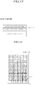
- FIG. 14 and FIG. 15 are plan views illustrating the organic light-emitting display panels 110 having a built-in touchscreen according to exemplary embodiments in which the M-TOE structure is used.
- FIG. 14 illustrates a case in which the touch electrodes TE are mesh-type touch electrodes having open areas.
- Two or more subpixels SP may be disposed below each of the touch electrodes TE.
- each of the touch electrodes TE must not block light emitted from two or more underlying subpixels SP.
- each of the open areas corresponds to each light-emitting area of the subpixels SP.
- the touch electrodes TE When the touch electrodes TE are mesh-type touch electrodes having open areas, the touch electrodes TE may be transparent electrodes or opaque electrodes.
- FIG. 15 illustrates a case in which the touch electrodes TE are bulk-type touch electrodes without open areas.
- Two or more subpixels SP may be disposed below each touch electrode TE.
- the touch electrode TE must not block light emitted from the two or more underlying subpixels SP.
- the touch electrodes TE when the touch electrodes TE are bulk-type touch electrodes without open areas, the touch electrodes TE may be transparent electrodes.
- each of the plurality of touch lines TL is electrically connected to one touch electrode TE among the number of touch electrodes TE.
- Each of the plurality of touch lines TL must be electrically connected to a specific touch electrode and must not be electrically connected to the other touch electrodes.
- the first touch sensor metal layer TSML1 in which the plurality of touch lines TL are disposed, overlap the second touch sensor metal layer TSML2, in which the plurality of touch electrodes TE are disposed.
- Each of the plurality of touch lines TL overlaps at least one touch electrode among the plurality of touch electrodes TE.
- the different types of touch sensor metals TE and TL disposed to overlap as described above can reduce peripheral areas (i.e. bezel areas) in which the touch sensor metals TE and TL are not disposed.
- each of the touch lines TL extends to a touch electrode TE electrically connected thereto.
- the touch lines TL may extend to the periphery of the display panel.
- each of the plurality of touch lines TL overlaps at least one touch electrode among the plurality of touch electrodes TE in the top-bottom direction
- the plurality of touch lines TL and the plurality of touch electrodes TE corresponding to the touch sensor metals are disposed in different touch sensor metal layers TSML1 and TSML2, whereby each touch line TL can be electrically isolated from non-corresponding touch electrodes TE.
- each of the plurality of touch lines TL overlaps at least one touch electrode among the plurality of touch electrodes TE
- the plurality of touch lines TL are located in a different layer from the plurality of touch electrodes TE, whereby each touch line TL can be electrically connected to a touch electrode among the plurality of touch electrodes TE corresponding thereto without being electrically isolated from the non-corresponding touch electrodes TE.
- the touch sensor metals can operate ordinarily, whereby touch sensing can be performed ordinarily.
- the plurality of touch lines TL corresponding to the touch sensor metals are electrically isolated from each other. Furthermore, the plurality of touch lines TL do not overlap each other.
- the plurality of touch electrodes TE corresponding to the touch sensor metals are electrically isolated from each other. Furthermore, the plurality of touch electrodes TE do not overlap each other.
- each touch electrode TE is connected to a corresponding touch line TL through a contract hole.
- a bridge a portion in which each touch electrode TE is connected to a corresponding touch line TL through a contract hole.
- FIG. 16 is a schematic view illustrating a first COE and M-TOE combination structure in the organic light-emitting display panel 110 having a built-in touchscreen according to exemplary embodiments.
- the first touch sensor metal layer TSML1 in which first touch sensor metals that may be the plurality of touch lines TL are located, is separated from the second touch sensor metal layer TSML2, in which second touch sensor metals that may be the plurality of touch electrodes TE are located, by an insulation layer IL.
- Each of the touch lines TL is electrically connected to a respective touch electrode TE corresponding thereto, through a contact hole (located in a bridge) extending through the insulation layer IL.
- the first touch sensor metal layer TSML1, insulation layer IL, and the second touch sensor metal layer TSML2 form a built-in touchscreen panel.
- the first touch sensor metal layer TSML1, insulation layer IL, and the second touch sensor metal layer TSML2 are disposed between the encapsulation layer L14 and the color filter layer CFL.
- the encapsulation layer L14, the built-in touchscreen panel TSML1, IL, and TSML2, and the color filter layer CFL are sequentially layered.
- the color filter layer CFL is located outward of the built-in touchscreen panel TSML1, IL, and TSML2 as described above, light that has been color-converted in the color filter layer CFL can be prevented from being distorted in the built-in touchscreen TSML1, IL, and TSML2. It is therefore possible to reduce the influence of the touch sensing structure on display performance.
- FIG. 17 is a cross-sectional view illustrating the first COE and M-TOE combination structure in the organic light-emitting display panel 110 having a built-in touchscreen according to exemplary embodiments.
- an overcoat layer OCL is disposed between the encapsulation layer L14 and the color filter layer CFL comprised of a plurality of patterned color filters CF.
- each of the subpixels SP may have a color filter CF disposed therein, the color of the color filter CF corresponding to the color of the subpixel.
- red color filters CF_R red color filters CF_R
- green color filters CF G green color filters CF G
- blue color filters CF_B are disposed in the color filter layer CFL.
- Black matrices BM may be respectively located between two adjacent subpixels SP.
- the plurality of touch electrodes TE and the plurality of touch lines TL are disposed between the encapsulation layer L14 and the overcoat layer OCL.
- FIG. 17 illustrates a single touch electrode among the plurality of mesh-type touch electrodes TE illustrated in FIG. 14 , the single touch electrode TE being closest to a touch pad TP, and a single touch line TL electrically connected to the single mesh-type touch electrode TE through a contact hole in the bridge.
- the positions of the open areas of the mesh-type touch electrodes TE illustrated in FIG. 17 correspond to the positions of the light-emitting areas of the subpixels.
- the positions of the light-emitting areas of the subpixels correspond to the positions of the first electrodes E1 of the subpixels, as well as the positions of the color filters CF corresponding to the subpixels.
- the first touch sensor metal layer TSML1 in which the plurality of touch lines TL are disposed, the insulation layer IL, and the second touch sensor metal layer TSML2 in which the plurality of touch electrodes TE are disposed, are disposed between the encapsulation layer L14 and the overcoat layer OCL.
- the built-in touchscreen panel including the first touch sensor metal layer TSML1, the insulation layer IL, and second touch sensor metal layer TSML2, is disposed between the encapsulation layer L14 and the overcoat layer OCL.
- the plurality of touch lines TL are disposed in the first touch sensor metal layer TSML1 on the encapsulation layer L14.
- the insulation layer IL is disposed on the first touch sensor metal layer TSML1.
- the plurality of touch electrodes TE are disposed in the second touch sensor metal layer TSML2 on the insulation layer IL.
- the overcoat layer OCL is disposed on the second touch sensor metal layer TSML2.
- the touch pads TP are located on the outer ends of the plurality of touch lines TL, respectively, in the first touch sensor metal layer TSML1, and are electrically connected to the touch sensing circuit TSC.
- FIG. 18 is a schematic view illustrating the process steps of fabricating the first COE and M-TOE combination structure in the organic light-emitting display panel 110 having a built-in touchscreen according to exemplary embodiments.
- a built-in touchscreen panel is fabricated on the encapsulation layer L14.
- the touch lines TL are disposed on the first touch sensor metal layer TSML1 on the encapsulation layer L14.
- the outer ends of the touch lines TL may act as the touch pads TP electrically connected to the touch sensing circuit TSC.
- An insulation layer IL is formed on the first touch sensor metal layer TSML1, and the plurality of touch electrodes TE are formed on the insulation layer IL to be located in the second touch sensor metal layer TSML2.
- the encapsulation layer L14 on which the built-in touchscreen panel is fabricated is covered with an overcoat layer OCL.
- black matrices BM are formed on the overcoat layer OCL, in positions corresponding to the boundaries of the subpixels
- the color filters CF corresponding to the light-emitting areas of the subpixels are patterned.
- the overcoat layer OCL is formed on the touch sensor metals, such as the touch lines TL, and the touch pads TP, and the touch electrodes TE, as described above, it is possible to protect the touch sensor metals TE and TL using the overcoat layer OCL.
- FIG. 19 is a schematic view illustrating a second COE and M-TOE combination structure in the organic light-emitting display panel 110 having a built-in touchscreen according to exemplary embodiments.
- the touch sensor metals including the plurality of touch electrodes TE and the plurality of touch lines TL, are disposed on the color filter layer CFL.
- the encapsulation layer L14, the color filter layer CFL, and the touch sensor metals TE, TL, and TP are sequentially layered.
- the first touch sensor metal layer TSML1 in which the plurality of touch lines TL are disposed is located on the color filter layer CFL, which is disposed on the encapsulation layer L14.
- the insulation layer IL is located on the first touch sensor metal layer TSML1 in which the plurality of touch lines TL are disposed, and the second touch sensor metal layer TSML2 in which the plurality of touch electrodes TE are disposed is located on the insulation layer IL.
- the first touch sensor metal layer TSML1 in which the plurality of touch lines TL are disposed, the insulation layer IL, the second touch sensor metal layer TSML2 in which the plurality of touch electrodes TE are disposed correspond to the built-in touchscreen panel disposed within the organic light-emitting display panel 110.
- the touch sensor metals e.g. the touch electrodes TE
- the distance between the touch pointer of the user to a touch electrode TE corresponding thereto may be reduced, thereby increasing the level of capacitance between the pointer and the corresponding touch electrode TE. Consequently, the accuracy of the operation of sensing a touch and a touched position can be improved.
- FIG. 20 is a cross-sectional view illustrating a second COE and M-TOE combination structure in the organic light-emitting display panel having a built-in touchscreen according to exemplary embodiments.
- the overcoat layer OCL is further disposed on the color filter layer CFL formed by patterning a plurality of color filters CF on the encapsulation layer L14.
- each of the subpixels SP may have a color filter CF disposed therein, the color of the color filter CF corresponding to the color of the subpixel.
- red color filters CF_R red color filters CF_R
- green color filters CF G green color filters CF G
- blue color filters CF_B are disposed in the color filter layer CFL.
- Black matrices BM may be respectively located between two adjacent subpixels SP.
- the overcoat layer OCL is disposed on the color filters CF.
- the touch sensor metals including the plurality of touch electrodes TE, the plurality of touch lines TL, and the plurality of touch pads TP, are disposed on the overcoat layer OCL.
- the first touch sensor metal layer TSML1 in which the plurality of touch lines TL are disposed, the insulation layer IL, and the second touch sensor metal layer TSML2 in which the plurality of touch electrodes TE are disposed are disposed on the overcoat layer OCL.
- the touch pads TP that may be connected to the touch lines TL or may be portions of the touch lines TL are located in the first touch sensor metal layer TSML1.
- the touch electrodes TE located in the second touch sensor metal layer TSML2 are electrically connected to the touch lines TL, located in the first touch sensor metal layer TSML1, through contact holes in the bridge area.
- FIG. 20 illustrates a single mesh-type touch electrode among the plurality of mesh-type touch electrodes TE illustrated in FIG. 14 , the single touch electrode TE being closest to a touch pad TP, and a single touch line TL electrically connected to the single mesh-type touch electrode TE through a contact hole in the bridge.
- the positions of the mesh-type touch electrodes TE illustrated in FIG. 20 correspond to the positions of the light-emitting areas of the subpixels.
- the positions of the light-emitting areas of the subpixels correspond to the positions of the first electrodes E1 of the subpixels, as well as the positions of the color filters CF corresponding to the subpixels.
- FIG. 21 is a schematic view illustrating the process steps of fabricating the second COE and M-TOE combination structure in the organic light-emitting display panel 110 having a built-in touchscreen according to exemplary embodiments.
- the black matrices BM are formed on boundaries of the subpixels.
- the color filters CF corresponding to the light-emitting areas of the subpixels are patterned.
- a built-in touchscreen panel is formed on the overcoat layer OCL.
- the touch electrodes TE, the touch lines TL, and the touch pads TP corresponding to the touch sensor metals forming the built-in touchscreen panel are formed on the overcoat layer OCL.
- the touch lines TL are located in the first touch sensor metal layer TSML1 on the overcoat layer OCL, the insulation layer IL is located on the first touch sensor metal layer TSML1, and the touch electrodes TE are located in the second touch sensor metal layer TSML2 on the insulation layer IL.
- the touch electrodes TE located in the second touch sensor metal layer TSML2 are electrically connected to the touch lines TL, located in the first touch sensor metal layer TSML1, through the contact holes in the bridge area.
- the touch pads TP connected to the touch lines TL or the touch pads TP corresponding to portions of the touch lines TL are located in the first touch sensor metal layer TSML1.
- the overcoat layer OCL is formed on the color filter layer CFL, and the touch sensor metals TE, TL, and TP are formed on the overcoat layer OCL. It is thereby possible to protect the color filter layer CFL and the patterns below the color filter layer CFL using the overcoat layer OCL.
- the overcoat layer OCL can prevent the touch electrodes TE, the touch lines TL, and the like from electrically interfering with electrodes, voltage lines, or signal lines located below the overcoat layer OCL.
- FIG. 22 is a schematic view illustrating the distance T defined between the touch electrode TE and the second electrode E2 and a parasitic capacitance component formed between the touch electrode TE and the second electrode E2 in the organic light-emitting display panel 110 having a built-in touchscreen according to exemplary embodiments.
- a touch driving signal TDS is applied to the touch electrode TE.
- a base voltage EVSS is applied to the second electrode E2 (e.g. cathode) of the OLED.
- the base voltage EVSS may be a DC voltage having a ground voltage value or a specific voltage value.
- the encapsulation layer L14 is disposed between the touch electrode TE and the second electrode E2 of the OLED.
- the encapsulation layer L14 is disposed between the touch electrode TE and the second electrode E2 of the OLED.
- the encapsulation layer L14 and the overcoat layer OCL are disposed between the touch electrode TE and the second electrode E2 of the OLED.
- parasitic capacitance Cpara may be formed between the touch electrode TE to which the touch driving signal TDS is applied and the second electrode E2 to which the base voltage EVSS is applied.
- the parasitic capacitance Cpara acts as a load increasing RC delay regarding the touch electrode TE and the touch line TL.
- the parasitic capacitance Cpara may change sensing data obtained from a signal received from the touch electrode TE to which the touch driving signal TDS is applied, thereby forming a touch sensing error.
- the organic light-emitting display panel 110 having a built-in touchscreen may have a structural feature able to prevent the parasitic capacitance Cpara. This feature will be described with reference to FIG. 23, FIG. 24 , and FIG. 25 .
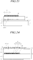
- FIG. 23 is a schematic view illustrating the distance T1 between the touch electrode TE and the second electrode E2 in the organic light-emitting display panel 110 having a built-in touchscreen and a first COE and M-TOE combination structure
- FIG. 24 is a schematic view illustrating the distance T2 between the touch electrode TE and the second electrode E2 in the organic light-emitting display panel 110 having a built-in touchscreen and a second COE and M-TOE combination structure
- FIG. 25 is a graph illustrating RC delay and touch sensing performance according to the distance T between the touch electrode TE and the second electrode E2 in the organic light-emitting display panel 110 having a built-in touchscreen according to exemplary embodiments.
- the distance T1 between the touch electrode TE and the second electrode E2 corresponds to the thickness of the encapsulation layer L14.
- the distance T2 between the touch electrode TE and the second electrode E2 corresponds to a total of the thickness of the encapsulation layer L14 and the thickness of the overcoat layer OCL.
- a decrease in the distance T between the touch electrode TE and the second electrode E2 increases the parasitic capacitance Cpara between the second electrode E2 and the touch electrode TE, thereby increasing RC delay and lowering touch sensing performance (touch sensitivity).
- an increase in the distance T between the touch electrode TE and the second electrode E2 reduces the parasitic capacitance Cpara between the second electrode E2 and the touch electrode TE, thereby decreasing RC delay and improving touch sensing performance (touch sensitivity).
- the distance T between the touch electrode TE and the second electrode E2 must be equal to or greater than a threshold thickness T_TH corresponding to maximum allowable RC delay KD and minimum touch sensing performance KP.
- the encapsulation layer L14 must be formed to be relatively thick, such that the distance T1 between the touch electrode TE and the second electrode E2 is equal to or greater than the threshold thickness T_TH.
- the encapsulation layer L14 and the overcoat layer OCL must be formed to be relatively thick such that the distance T2 between the touch electrode TE and the second electrode E2 is equal to or greater than the threshold thickness T_TH.
- the distance T1 between the touch electrode TE and the second electrode E2 in the organic light-emitting display panel 110 having a built-in touchscreen in which the first COE and M-TOE combination structure illustrated in FIG. 23 is provided or the distance T2 between the touch electrode TE and the second electrode E2 in the organic light-emitting display panel 110 having a built-in touchscreen in which the second COE and M-TOE combination structure illustrated in FIG. 24 is provided may be equal to the distance between the plurality of touch electrodes TE and the bottom surface of the encapsulation layer L14 (i.e. the top surface of the second electrode E2).
- the threshold thickness T_TH may be 5 ⁇ m.
- the distance between the plurality of touch electrodes TE and the bottom surface of the encapsulation layer L14 may be designed to be equal to or greater than 5 ⁇ m.
- each of the high-resistance black matrices BM is disposed between two adjacent color filters among the color filters CF in the color filter layer CFL.
- the resistance of the high-resistance black matrices BM is equal to or higher than a predetermined level of resistance.
- the touch sensor metals can be reliably disposed within the organic light-emitting display panel 110 including an organic material.
- the distance between the second electrode E2 and the touch electrode TE (i.e. the distance between the bottom surface of the encapsulation layer L14 and the touch electrode TE) is designed to be equal to or greater than a predetermined value T_TH of, for example, 5 ⁇ m, whereby the parasitic capacitance Cpara can be prevented from being formed between the second electrode E2 and the touch electrode TE.
- the structural design change (e.g. the changed thickness) can prevent the parasitic capacitance Cpara from being formed between the second electrode E2 and the touch electrode TE.
- load-free driving performed during the touch mode section can prevent the parasitic capacitance Cpara from being formed between the second electrode E2 and the touch electrode TE.
- FIG. 26 is a schematic view illustrating load-free driving for removing a parasitic capacitance component from the organic light-emitting display device 100 having a built-in touchscreen according to exemplary embodiments.
- the organic light-emitting display device 100 having a built-in touchscreen performs load-free driving of applying a load-free driving signal LFDS to the second electrode E2 to reduce the potential difference between the second electrode E2 and the touch electrode TE, thereby being able to prevent parasitic capacitance Cpara from being formed between the second electrode E2 and the touch electrode TE.
- the load-free driving signal LFDS may be a signal identical to the touch driving signal TDS or a signal corresponding to the touch driving signal TDS.
- At least one of the frequency, phase, and amplitude of the load-free driving signal TDS may be identical to a corresponding one of the frequency, phase, and amplitude of the touch driving signal TDS.
- the signal output characteristics of the organic light-emitting display device 100 having a built-in touchscreen can be controlled such that at least one of the frequency, phase, and amplitude of the load-free driving signal TDS becomes identical to a corresponding one of the frequency, phase, and amplitude of the touch driving signal TDS at a point at which the load-free driving signal TDS is actually applied to the second electrode E2 and a point at which the touch driving signal TDS is actually applied to the touch electrode TE.
- the signal output characteristics of the load-free driving signal TDS and the touch driving signal TDS are controlled by a signal output configuration such that at least one of the frequency, phase, and amplitude of the load-free driving signal TDS becomes identical to a corresponding one of the frequency, phase, and amplitude of the touch driving signal TDS at the point at which the load-free driving signal TDS is actually applied to the second electrode E2 and the point at which the touch driving signal TDS is actually applied to the touch electrode TE, at least one of the frequency, phase, and amplitude of the load-free driving signal TDS may differ from a corresponding one of the frequency, phase, and amplitude of the touch driving signal TDS at a point at which the load-free driving signal TDS and the touch driving signal TDS are output.
- the organic light-emitting display panel 110 having a built-in touchscreen and the organic light-emitting display device 100 having a built-in touchscreen are provided with a structure enabling a touchscreen panel (i.e. touch sensor metals) to be disposed therewithin.
- a touchscreen panel i.e. touch sensor metals
- the organic light-emitting display panel 110 having a built-in touchscreen and the organic light-emitting display device 100 having a built-in touchscreen can improve touch sensing performance.
- the organic light-emitting display panel 110 having a built-in touchscreen and the organic light-emitting display device 100 having a built-in touchscreen are provided with a structure enabling an ultrathin profile to be designed.
- the organic light-emitting display panel 110 having a built-in touchscreen and the organic light-emitting display device 100 having a built-in touchscreen are provided with a touchscreen panel (i.e. touch sensor metals) disposed therewithin without display performance being influenced.
- a touchscreen panel i.e. touch sensor metals
- the organic light-emitting display panel 110 having a built-in touchscreen and the organic light-emitting display device 100 having a built-in touchscreen are provided with an M-TOE structure in which two touch sensor metals (touch electrodes and touch lines) are disposed in different layers, the touch sensor metals enabling self-capacitance based touch sensing.
Landscapes
- Engineering & Computer Science (AREA)
- General Engineering & Computer Science (AREA)
- Theoretical Computer Science (AREA)
- Physics & Mathematics (AREA)
- Human Computer Interaction (AREA)
- General Physics & Mathematics (AREA)
- Optics & Photonics (AREA)
- Computer Networks & Wireless Communication (AREA)
- Electroluminescent Light Sources (AREA)
- Devices For Indicating Variable Information By Combining Individual Elements (AREA)
- Optical Filters (AREA)
- Geometry (AREA)
- Microelectronics & Electronic Packaging (AREA)
Claims (15)
- Panneau d'affichage électroluminescent organique (110) ayant un écran tactile intégré avec un motif de détection tactile incluant une pluralité d'électrodes tactiles (TE), une pluralité de lignes tactiles (TL) et une pluralité de micropavés tactiles (TP), le panneau d'affichage (110) comportant une pluralité de sous-pixels (SP) définis dans celui-ci par une pluralité de lignes de données (DL) et une pluralité de lignes de grille (GL) et la pluralité d'électrodes tactiles (TE) disposées sur celles-ci ; etun circuit de détection tactile (TSC) fournissant un signal de commande tactile (TDS) à au moins une électrode tactile (TE) parmi la pluralité d'électrodes tactiles (TE) et détectant au moins un élément parmi un toucher et une position touchée sur la base d'un signal détecté en utilisant chaque électrode de la pluralité d'électrodes tactiles (TE) auxquelles le signal de commande tactile (TDS) est appliqué,dans lequel le panneau d'affichage électroluminescent organique (110) comporte en outre une couche d'encapsulation (L14) et une couche de filtres à couleur (CFL) située sur la couche d'encapsulation (L14),dans lequel la pluralité d'électrodes tactiles (TE) est située sur la couche d'encapsulation (L14),dans lequel la pluralité de lignes tactiles (TL) est située sur la couche d'encapsulation (L14) pour connecter électriquement la pluralité d'électrodes tactiles (TE) au circuit de détection tactile (TSC), dans lequel sur chaque ligne de la pluralité de lignes tactiles (TL) est disposé un micropavé de la pluralité de micropavés tactiles (TP), la pluralité de micropavés tactiles (TP) étant électriquement connectée au circuit de détection tactile (TSC),dans lequel la pluralité d'électrodes tactiles (TE) et la pluralité de lignes tactiles (TL) sont disposées dans différentes couches entre lesquelles une couche d'isolation (IL) est prise en sandwich,dans lequel chaque ligne de la pluralité de lignes tactiles (TL) est électriquement connectée à une électrode tactile (TE) correspondante de la pluralité d'électrodes tactiles (TE) à travers un trou de contact,dans lequel chaque ligne de la pluralité de lignes tactiles (TL) est électriquement isolée des électrodes tactiles (TE) restantes,dans lequel la pluralité de micropavés tactiles (TP) est située sur la même couche que la pluralité de lignes tactiles (TL) et une partie de chacun des micropavés tactiles (TP) ne recouvre pas la couche d'isolation (IL).
- Panneau d'affichage électroluminescent organique (110) selon la revendication 1, dans lequel chaque ligne de la pluralité de lignes tactiles recouvre au moins une électrode tactile (TE) de la pluralité d'électrodes tactiles (TE).
- Panneau d'affichage électroluminescent organique (110) selon l'une des revendications 1 ou 2,dans lequel la pluralité de lignes tactiles (TL) est disposée dans une première couche métallique de capteur tactile sur la couche d'encapsulation (L14), la couche d'isolation étant disposée sur la première couche métallique de capteur tactile,dans lequel la pluralité d'électrodes tactiles (TE) est disposée dans une seconde couche métallique de capteur tactile sur la couche d'isolation, etdans lequel un micropavé tactile est prévu sur chaque extrémité extérieure de la pluralité de lignes tactiles (TL), le micropavé tactile étant électriquement connecté au circuit de détection tactile (TSC) et situé dans la première couche métallique de capteur tactile.
- Panneau d'affichage électroluminescent organique (110) selon l'une des revendications précédentes, dans lequel la pluralité d'électrodes tactiles (TE) est disposée entre la couche d'encapsulation (L14) et la couche de filtres à couleur (CFL).
- Panneau d'affichage électroluminescent organique (110) selon la revendication 4, dans lequel le panneau d'affichage électroluminescent organique (110) comporte en outre :une couche de revêtement de finition (OCL) disposée entre la couche d'encapsulation (L14) et la couche de filtres à couleur (CFL), etla pluralité d'électrodes tactiles (TE) est disposée entre la couche d'encapsulation (L14) et la couche de revêtement de finition (OCL).
- Panneau d'affichage électroluminescent organique (110) selon les revendications 1 à 3, dans lequel la pluralité d'électrodes tactiles (TE) est disposée sur la couche de filtres à couleur (CFL).
- Panneau d'affichage électroluminescent organique (110) selon la revendication 6, dans lequel le panneau d'affichage électroluminescent organique (110) comporte en outre une couche de revêtement de finition (OCL) disposée sur la couche de filtres à couleur (CFL), et les électrodes de la pluralité d'électrodes tactiles (TE) sont disposées sur la couche de revêtement de finition (OCL).
- Panneau d'affichage électroluminescent organique selon l'une des revendications précédentes, dans lequel chaque électrode de la pluralité d'électrodes tactiles (TE) comporte une électrode transparente de type massif avec une zone ouverte (OA).
- Panneau d'affichage électroluminescent organique selon l'une des revendications précédentes, dans lequel chaque électrode de la pluralité d'électrodes tactiles (TE) comporte une électrode transparente ou opaque de type à mailles ayant une zone ouverte (OA).
- Panneau d'affichage électroluminescent organique selon l'une des revendications précédentes, dans lequel une taille de chaque électrode de la pluralité d'électrodes tactiles (TE) est supérieure à une taille de chaque sous-pixel de la pluralité de sous-pixels (SP) ; et/ou
dans lequel une distance entre la pluralité d'électrodes tactiles (TE) et une surface inférieure de la couche d'encapsulation (L14) est égale ou supérieure à 5 µm. - Panneau d'affichage électroluminescent organique selon l'une des revendications précédentes, dans lequel deux lignes de grille (GL) ou plus parmi la pluralité de lignes de grille (GL) ou deux lignes de données (DL) ou plus parmi la pluralité de lignes de données (DL) sont disposées dans une zone occupée par chaque électrode de la pluralité d'électrodes tactiles (TE).
- Panneau d'affichage électroluminescent organique (110) selon l'une des revendications précédentes, dans lequel chaque sous-pixel de la pluralité de sous-pixels (SP) comporte :une diode électroluminescente organique (OLED) comportant une première électrode (E1), une couche électroluminescente organique (EL) et une seconde électrode (E2) ;un transistor d'attaque (DRT) attaquant la diode électroluminescente organique (OLED) ;un premier transistor (T1) électriquement connecté entre un premier nœud (N1) du transistor d'attaque (DRT) et une ligne de données (DL) parmi la pluralité de lignes de données (DL) correspondant à celui-ci ; etun condensateur de stockage (C1) électriquement connecté entre le premier nœud (N1) et un second nœud (N2) du transistor d'attaque (DRT) ;dans lequel la couche d'encapsulation (L14) est située sur la seconde électrode (E2) de la diode électroluminescente organique (OLED) ;dans lequel la couche de filtres à couleur (CFL) est située sur la couche d'encapsulation (L14) ; etdans lequel la pluralité d'électrodes tactiles (TE) correspond au capteur tactile et est située sur la couche d'encapsulation (L14),dans lequel un signal de commande tactile (TDS) est fourni à au moins une électrode tactile (TE) parmi la pluralité d'électrodes tactiles (TE), etdans lequel l'électrode tactile (TE) à laquelle le signal de commande tactile (TDS) est appliqué forme une capacité en association avec un pointeur correspondant à un moyen d'opération de toucher d'un utilisateur.
- Panneau d'affichage électroluminescent organique (110) selon l'une des revendications précédentes, comportant en outre une matrice noire (BM) disposée entre deux filtres à couleur (CF) adjacents dans la couche de filtres à couleur (CFL), une résistance de la matrice noire (BM) étant égale ou supérieure à un niveau de résistance prédéterminé.
- Panneau d'affichage électroluminescent organique (110) selon les revendications 12 ou 13, dans lequel un signal de commande sans charge (LFDS) étant identique ou correspondant au signal de commande tactile (TDS) est appliqué aux secondes électrodes (E2), dans lequel de préférence au moins un élément parmi la fréquence, la phase et l'amplitude du signal de commande sans charge (LFDS) est identique à une fréquence, une phase et une amplitude correspondantes du signal de commande tactile (TDS).
- Dispositif d'affichage électroluminescent organique (100) comportant un panneau d'affichage électroluminescent organique (110) selon l'une des revendications précédentes.
Applications Claiming Priority (1)
| Application Number | Priority Date | Filing Date | Title |
|---|---|---|---|
| KR1020160122352A KR102679093B1 (ko) | 2016-09-23 | 2016-09-23 | 터치스크린 내장형 유기발광표시패널 및 유기발광표시장치 |
Publications (2)
| Publication Number | Publication Date |
|---|---|
| EP3299940A1 EP3299940A1 (fr) | 2018-03-28 |
| EP3299940B1 true EP3299940B1 (fr) | 2022-11-30 |
Family
ID=57629506
Family Applications (1)
| Application Number | Title | Priority Date | Filing Date |
|---|---|---|---|
| EP16207505.5A Active EP3299940B1 (fr) | 2016-09-23 | 2016-12-30 | Panneau d'affichage électroluminescent organique et afficheur électroluminescent organique intégrant un écran tactile |
Country Status (6)
| Country | Link |
|---|---|
| US (1) | US10386956B2 (fr) |
| EP (1) | EP3299940B1 (fr) |
| JP (2) | JP6466394B2 (fr) |
| KR (2) | KR102679093B1 (fr) |
| CN (1) | CN107871760B (fr) |
| TW (1) | TWI627570B (fr) |
Families Citing this family (25)
| Publication number | Priority date | Publication date | Assignee | Title |
|---|---|---|---|---|
| KR102561120B1 (ko) | 2016-09-23 | 2023-07-28 | 엘지디스플레이 주식회사 | 터치스크린 내장형 유기발광표시패널 및 유기발광표시장치 |
| KR101974086B1 (ko) * | 2016-09-30 | 2019-05-02 | 삼성디스플레이 주식회사 | 표시모듈 |
| KR102608954B1 (ko) * | 2016-09-30 | 2023-12-05 | 삼성디스플레이 주식회사 | 표시 장치 |
| JP6885134B2 (ja) * | 2017-03-24 | 2021-06-09 | セイコーエプソン株式会社 | 電気光学装置、電気光学装置の製造方法、電子機器 |
| CN107180852B (zh) * | 2017-05-18 | 2019-11-15 | 上海天马有机发光显示技术有限公司 | 一种触控显示面板及显示装置 |
| CN107275512A (zh) * | 2017-05-25 | 2017-10-20 | 厦门天马微电子有限公司 | 一种有机电致发光显示面板、其制作方法及显示装置 |
| KR102325262B1 (ko) * | 2017-06-01 | 2021-11-10 | 엘지디스플레이 주식회사 | 터치 디스플레이 장치, 터치 디스플레이 패널 및 터치 디스플레이 패널의 제조 방법 |
| CN108470753B (zh) * | 2018-03-28 | 2021-02-26 | 京东方科技集团股份有限公司 | 一种电致发光显示面板、其制作方法及显示装置 |
| KR101918146B1 (ko) * | 2018-04-27 | 2018-11-13 | 셀로코아이엔티 주식회사 | 인셀 터치표시장치 및 그 제조방법 |
| KR102534689B1 (ko) * | 2018-06-14 | 2023-05-19 | 엘지디스플레이 주식회사 | 터치표시장치, 데이터구동회로 및 구동방법 |
| KR102575506B1 (ko) * | 2018-07-19 | 2023-09-05 | 엘지디스플레이 주식회사 | 터치 센서를 구비하는 표시장치 |
| KR102536348B1 (ko) * | 2018-07-19 | 2023-05-24 | 엘지디스플레이 주식회사 | 터치 센서를 가지는 표시 장치 |
| WO2020149139A1 (fr) * | 2019-01-16 | 2020-07-23 | 株式会社小糸製作所 | Appareil d'imagerie, dispositif de traitement informatique associé, appareil d'éclairage pour véhicule, véhicule et procédé de détection |
| KR102792468B1 (ko) | 2019-07-24 | 2025-04-08 | 엘지디스플레이 주식회사 | 터치 전극들을 포함하는 디스플레이 장치 |
| US20210065627A1 (en) * | 2019-08-27 | 2021-03-04 | Novatek Microelectronics Corp. | Control method for OLED touch panel and related touch and OLED driver |
| CN112631450A (zh) * | 2019-10-09 | 2021-04-09 | 群创光电股份有限公司 | 电子装置 |
| KR102384388B1 (ko) * | 2019-12-18 | 2022-04-07 | 엘지디스플레이 주식회사 | 터치 디스플레이 장치 |
| KR102914155B1 (ko) * | 2019-12-30 | 2026-01-16 | 엘지디스플레이 주식회사 | 유기 발광 표시 장치 |
| US10908752B1 (en) * | 2020-02-14 | 2021-02-02 | Novatek Microelectronics Corp. | Display panel with touch sensor |
| CN111509141B (zh) * | 2020-05-06 | 2023-08-01 | 上海天马微电子有限公司 | 一种显示面板及其制备方法、显示装置 |
| KR102915438B1 (ko) * | 2020-10-30 | 2026-01-20 | 엘지디스플레이 주식회사 | 터치 디스플레이 장치 |
| US12127460B2 (en) * | 2020-12-30 | 2024-10-22 | Lg Display Co., Ltd. | Display panel and display device |
| JP2023106247A (ja) * | 2022-01-20 | 2023-08-01 | シャープディスプレイテクノロジー株式会社 | タッチパネル付き表示装置及びタッチパネル |
| KR20240068460A (ko) * | 2022-11-10 | 2024-05-17 | 엘지디스플레이 주식회사 | 터치 표시 장치 및 터치 센싱 방법 |
| KR102593283B1 (ko) * | 2023-04-27 | 2023-10-25 | (주)파인디어칩 | Led 매트릭스의 이상발광현상 제거기능을 구비한 led 제어장치 |
Citations (1)
| Publication number | Priority date | Publication date | Assignee | Title |
|---|---|---|---|---|
| US20180113364A1 (en) * | 2016-05-04 | 2018-04-26 | Wuhan China Star Optoelectronics Technology Co., Ltd. | In-cell touch liquid crystal panel and array substrate thereof |
Family Cites Families (50)
| Publication number | Priority date | Publication date | Assignee | Title |
|---|---|---|---|---|
| JP2705652B2 (ja) * | 1995-07-28 | 1998-01-28 | 日本電気株式会社 | 透過型液晶表示装置 |
| KR100669773B1 (ko) * | 2004-11-18 | 2007-01-16 | 삼성에스디아이 주식회사 | 유기전계 발광표시장치 및 그의 제조방법 |
| US8928597B2 (en) | 2008-07-11 | 2015-01-06 | Samsung Display Co., Ltd. | Organic light emitting display device |
| KR101634791B1 (ko) | 2008-11-28 | 2016-06-30 | 삼성디스플레이 주식회사 | 접촉 감지 기능이 있는 유기 발광 표시 장치 |
| JP2010181747A (ja) * | 2009-02-06 | 2010-08-19 | Seiko Instruments Inc | タッチセンサ機能付液晶表示装置 |
| JP5306059B2 (ja) | 2009-05-29 | 2013-10-02 | 株式会社ジャパンディスプレイウェスト | タッチパネル、表示パネル、タッチパネル用基板、表示パネル用基板および表示装置 |
| JP2011023558A (ja) * | 2009-07-16 | 2011-02-03 | Sharp Corp | 有機el表示装置 |
| KR101071162B1 (ko) * | 2010-05-17 | 2011-10-10 | 이성호 | 충전식 터치스크린 패널 |
| KR101085088B1 (ko) * | 2010-09-01 | 2011-11-18 | 이성호 | 레벨시프트를 이용한 정전식 터치 검출수단, 검출방법 및 터치스크린패널과, 그러한 정전식 터치스크린패널을 내장한 표시장치 |
| JP5789113B2 (ja) * | 2011-03-31 | 2015-10-07 | 株式会社Joled | 表示装置および電子機器 |
| WO2013018591A1 (fr) * | 2011-07-29 | 2013-02-07 | シャープ株式会社 | Substrat d'écran tactile et dispositif électro-optique |
| US8994673B2 (en) | 2011-12-09 | 2015-03-31 | Lg Display Co., Ltd. | Display device with integrated touch screen having electrical connections provided in inactive regions of display panel |
| US9910301B2 (en) * | 2012-02-23 | 2018-03-06 | Switch Materials, Inc. | Switchable optical filter apparatus with light |
| JP2015111318A (ja) * | 2012-03-22 | 2015-06-18 | シャープ株式会社 | カラーフィルター一体型タッチパネル |
| US9214507B2 (en) * | 2012-08-17 | 2015-12-15 | Apple Inc. | Narrow border organic light-emitting diode display |
| KR102245511B1 (ko) | 2012-12-27 | 2021-04-28 | 엘지디스플레이 주식회사 | 플렉서블 유기 발광 표시 장치 및 플렉서블 유기 발광 표시 장치 제조 방법 |
| JP5827972B2 (ja) * | 2013-04-17 | 2015-12-02 | ジオマテック株式会社 | タッチセンサ一体型表示装置 |
| CN110045886B (zh) * | 2013-07-08 | 2022-09-27 | 益逻触控系统公司 | 触摸传感方法、触摸传感系统及计算机可读设备 |
| JP6253923B2 (ja) | 2013-08-30 | 2017-12-27 | 株式会社ジャパンディスプレイ | タッチセンサ内蔵有機エレクトロルミネッセンス装置 |
| JP6097663B2 (ja) * | 2013-09-12 | 2017-03-15 | 株式会社ジャパンディスプレイ | タッチパネル機能内蔵表示装置 |
| JP2015072663A (ja) * | 2013-10-04 | 2015-04-16 | 株式会社ジャパンディスプレイ | 表示装置 |
| KR101984443B1 (ko) | 2013-12-13 | 2019-05-30 | 애플 인크. | 자기-정전용량성 터치 센서를 위한 통합된 터치 및 디스플레이 아키텍처 |
| TWM480722U (zh) | 2014-01-06 | 2014-06-21 | Superc Touch Corp | 高準確度之窄邊框內嵌式平面顯示觸控結構 |
| JP2015143933A (ja) | 2014-01-31 | 2015-08-06 | 株式会社ジャパンディスプレイ | 静電容量型センサ付き表示装置及びその駆動方法 |
| KR102193915B1 (ko) * | 2014-02-10 | 2020-12-23 | 삼성디스플레이 주식회사 | 터치 센서 기판 및 이를 포함하는 표시 장치 |
| TWM491878U (zh) | 2014-05-29 | 2014-12-11 | Superc Touch Corp | 以透明感應電極連接金屬走線的觸控顯示結構 |
| JP2016004280A (ja) * | 2014-06-13 | 2016-01-12 | 株式会社ジャパンディスプレイ | タッチ検出装置及びタッチ検出機能付き表示装置 |
| KR101648571B1 (ko) * | 2014-07-16 | 2016-08-18 | 엘지디스플레이 주식회사 | 인 셀 터치 타입의 표시장치 |
| KR102173545B1 (ko) * | 2014-08-05 | 2020-11-04 | 엘지디스플레이 주식회사 | 인 셀 타입의 터치 구조를 갖는 유기발광표시장치 |
| KR101671578B1 (ko) * | 2014-08-11 | 2016-11-02 | 엘지디스플레이 주식회사 | 터치센서 일체형 표시장치 |
| JP6255107B2 (ja) * | 2014-08-28 | 2017-12-27 | 富士フイルム株式会社 | 加飾材付き基材、加飾層形成用転写材料、タッチパネル、及び、情報表示装置 |
| KR102326807B1 (ko) * | 2014-11-26 | 2021-11-15 | 엘지디스플레이 주식회사 | 유기발광표시장치 및 이의 제조방법 |
| CN105843433B (zh) * | 2015-01-30 | 2019-01-18 | 乐金显示有限公司 | 触摸显示设备 |
| KR102283002B1 (ko) | 2015-02-16 | 2021-07-30 | 삼성디스플레이 주식회사 | 표시장치 |
| KR102352406B1 (ko) * | 2015-03-02 | 2022-01-19 | 삼성디스플레이 주식회사 | 표시 장치의 제조 방법 및 표시 장치 |
| US10133426B2 (en) * | 2015-06-18 | 2018-11-20 | X-Celeprint Limited | Display with micro-LED front light |
| US10168844B2 (en) * | 2015-06-26 | 2019-01-01 | Samsung Display Co., Ltd. | Flexible display device |
| KR102369933B1 (ko) * | 2015-08-03 | 2022-03-04 | 삼성전자주식회사 | 반도체 발광소자 및 그 제조 방법 |
| KR102390448B1 (ko) * | 2015-08-25 | 2022-04-26 | 삼성디스플레이 주식회사 | 커브드 디스플레이 장치 |
| KR102438247B1 (ko) * | 2015-09-07 | 2022-08-30 | 엘지디스플레이 주식회사 | 유기 발광 표시 장치 및 이의 제조 방법 |
| KR101750428B1 (ko) * | 2015-09-24 | 2017-06-23 | 엘지디스플레이 주식회사 | 터치 스크린 일체형 표시장치 |
| CN106783909A (zh) * | 2015-11-19 | 2017-05-31 | 京东方科技集团股份有限公司 | 一种触摸屏、其制作方法及显示装置 |
| KR102421871B1 (ko) * | 2015-11-30 | 2022-07-19 | 엘지디스플레이 주식회사 | 터치스크린 내장형 표시장치 |
| KR102536250B1 (ko) * | 2016-03-17 | 2023-05-25 | 삼성디스플레이 주식회사 | 디스플레이 장치 |
| US10283574B2 (en) * | 2016-03-25 | 2019-05-07 | Samsung Display Co., Ltd. | Display apparatus with bending area capable of minimizing manufacturing defects |
| KR102514411B1 (ko) * | 2016-03-31 | 2023-03-28 | 삼성디스플레이 주식회사 | 디스플레이 장치 및 그 제조방법 |
| KR102572720B1 (ko) * | 2016-05-03 | 2023-08-31 | 삼성디스플레이 주식회사 | 디스플레이 장치 및 그 제조방법 |
| KR20180006519A (ko) * | 2016-07-07 | 2018-01-18 | 삼성디스플레이 주식회사 | 터치 센서 및 이를 포함하는 표시 장치 |
| KR102668184B1 (ko) * | 2016-07-25 | 2024-05-24 | 삼성디스플레이 주식회사 | 표시 장치 |
| KR102557892B1 (ko) * | 2016-08-19 | 2023-07-21 | 삼성디스플레이 주식회사 | 디스플레이 장치 |
-
2016
- 2016-09-23 KR KR1020160122352A patent/KR102679093B1/ko active Active
- 2016-12-27 JP JP2016253761A patent/JP6466394B2/ja active Active
- 2016-12-27 US US15/391,625 patent/US10386956B2/en active Active
- 2016-12-28 CN CN201611233480.1A patent/CN107871760B/zh active Active
- 2016-12-28 TW TW105143710A patent/TWI627570B/zh active
- 2016-12-30 EP EP16207505.5A patent/EP3299940B1/fr active Active
-
2019
- 2019-01-08 JP JP2019001234A patent/JP6767522B2/ja active Active
-
2024
- 2024-06-24 KR KR1020240081816A patent/KR102861579B1/ko active Active
Patent Citations (1)
| Publication number | Priority date | Publication date | Assignee | Title |
|---|---|---|---|---|
| US20180113364A1 (en) * | 2016-05-04 | 2018-04-26 | Wuhan China Star Optoelectronics Technology Co., Ltd. | In-cell touch liquid crystal panel and array substrate thereof |
Also Published As
| Publication number | Publication date |
|---|---|
| JP6767522B2 (ja) | 2020-10-14 |
| TW201814460A (zh) | 2018-04-16 |
| KR102679093B1 (ko) | 2024-06-28 |
| KR102861579B1 (ko) | 2025-09-19 |
| CN107871760B (zh) | 2021-08-31 |
| JP2018049253A (ja) | 2018-03-29 |
| KR20240100337A (ko) | 2024-07-01 |
| KR20180033360A (ko) | 2018-04-03 |
| US10386956B2 (en) | 2019-08-20 |
| CN107871760A (zh) | 2018-04-03 |
| TWI627570B (zh) | 2018-06-21 |
| EP3299940A1 (fr) | 2018-03-28 |
| JP6466394B2 (ja) | 2019-02-06 |
| US20180088726A1 (en) | 2018-03-29 |
| JP2019110127A (ja) | 2019-07-04 |
Similar Documents
| Publication | Publication Date | Title |
|---|---|---|
| EP3299940B1 (fr) | Panneau d'affichage électroluminescent organique et afficheur électroluminescent organique intégrant un écran tactile | |
| US10949038B2 (en) | Organic light-emitting display panel and organic light-emitting display device having built-in touchscreen | |
| US10955952B2 (en) | Display panel having built-in touchscreen, display device having built-in touch screen, integrated driving circuit, and driving method | |
| US10908721B2 (en) | Touch display panel and touch display device for removing display noise from a touch sensing signal | |
| US10739889B2 (en) | Touch display device and touch display panel | |
| CN109696998B (zh) | 触摸显示设备和面板 | |
| EP3767445B1 (fr) | Panneau d'affichage et dispositif d'affichage tactile | |
| KR20190055940A (ko) | 터치표시장치 및 패널 | |
| US12069916B2 (en) | Touch display device with short circuit prevention electrode | |
| KR20180049326A (ko) | 터치 스크린 내장형 유기발광표시패널 및 유기발광표시장치 | |
| KR102802246B1 (ko) | 터치 회로, 터치 디스플레이 장치 및 구동 방법 |
Legal Events
| Date | Code | Title | Description |
|---|---|---|---|
| PUAI | Public reference made under article 153(3) epc to a published international application that has entered the european phase |
Free format text: ORIGINAL CODE: 0009012 |
|
| STAA | Information on the status of an ep patent application or granted ep patent |
Free format text: STATUS: REQUEST FOR EXAMINATION WAS MADE |
|
| 17P | Request for examination filed |
Effective date: 20161230 |
|
| AK | Designated contracting states |
Kind code of ref document: A1 Designated state(s): AL AT BE BG CH CY CZ DE DK EE ES FI FR GB GR HR HU IE IS IT LI LT LU LV MC MK MT NL NO PL PT RO RS SE SI SK SM TR |
|
| AX | Request for extension of the european patent |
Extension state: BA ME |
|
| RBV | Designated contracting states (corrected) |
Designated state(s): AL AT BE BG CH CY CZ DE DK EE ES FI FR GB GR HR HU IE IS IT LI LT LU LV MC MK MT NL NO PL PT RO RS SE SI SK SM TR |
|
| R17P | Request for examination filed (corrected) |
Effective date: 20161230 |
|
| STAA | Information on the status of an ep patent application or granted ep patent |
Free format text: STATUS: EXAMINATION IS IN PROGRESS |
|
| 17Q | First examination report despatched |
Effective date: 20210312 |
|
| REG | Reference to a national code |
Ref country code: DE Ref legal event code: R079 Ref document number: 602016076580 Country of ref document: DE Free format text: PREVIOUS MAIN CLASS: G06F0003041000 Ipc: H01L0027320000 |
|
| GRAP | Despatch of communication of intention to grant a patent |
Free format text: ORIGINAL CODE: EPIDOSNIGR1 |
|
| STAA | Information on the status of an ep patent application or granted ep patent |
Free format text: STATUS: GRANT OF PATENT IS INTENDED |
|
| RIC1 | Information provided on ipc code assigned before grant |
Ipc: H01L 51/52 20060101ALI20220513BHEP Ipc: G06F 3/044 20060101ALI20220513BHEP Ipc: G06F 3/041 20060101ALI20220513BHEP Ipc: H01L 27/32 20060101AFI20220513BHEP |
|
| INTG | Intention to grant announced |
Effective date: 20220609 |
|
| GRAS | Grant fee paid |
Free format text: ORIGINAL CODE: EPIDOSNIGR3 |
|
| GRAA | (expected) grant |
Free format text: ORIGINAL CODE: 0009210 |
|
| STAA | Information on the status of an ep patent application or granted ep patent |
Free format text: STATUS: THE PATENT HAS BEEN GRANTED |
|
| REG | Reference to a national code |
Ref country code: DE Ref legal event code: R079 Ref document number: 602016076580 Country of ref document: DE Free format text: PREVIOUS MAIN CLASS: H01L0027320000 Ipc: H10K0059000000 |
|
| AK | Designated contracting states |
Kind code of ref document: B1 Designated state(s): AL AT BE BG CH CY CZ DE DK EE ES FI FR GB GR HR HU IE IS IT LI LT LU LV MC MK MT NL NO PL PT RO RS SE SI SK SM TR |
|
| REG | Reference to a national code |
Ref country code: CH Ref legal event code: EP Ref country code: GB Ref legal event code: FG4D |
|
| REG | Reference to a national code |
Ref country code: AT Ref legal event code: REF Ref document number: 1535343 Country of ref document: AT Kind code of ref document: T Effective date: 20221215 Ref country code: DE Ref legal event code: R096 Ref document number: 602016076580 Country of ref document: DE |
|
| REG | Reference to a national code |
Ref country code: IE Ref legal event code: FG4D |
|
| REG | Reference to a national code |
Ref country code: LT Ref legal event code: MG9D |
|
| REG | Reference to a national code |
Ref country code: NL Ref legal event code: MP Effective date: 20221130 |
|
| PG25 | Lapsed in a contracting state [announced via postgrant information from national office to epo] |
Ref country code: SE Free format text: LAPSE BECAUSE OF FAILURE TO SUBMIT A TRANSLATION OF THE DESCRIPTION OR TO PAY THE FEE WITHIN THE PRESCRIBED TIME-LIMIT Effective date: 20221130 Ref country code: PT Free format text: LAPSE BECAUSE OF FAILURE TO SUBMIT A TRANSLATION OF THE DESCRIPTION OR TO PAY THE FEE WITHIN THE PRESCRIBED TIME-LIMIT Effective date: 20230331 Ref country code: NO Free format text: LAPSE BECAUSE OF FAILURE TO SUBMIT A TRANSLATION OF THE DESCRIPTION OR TO PAY THE FEE WITHIN THE PRESCRIBED TIME-LIMIT Effective date: 20230228 Ref country code: LT Free format text: LAPSE BECAUSE OF FAILURE TO SUBMIT A TRANSLATION OF THE DESCRIPTION OR TO PAY THE FEE WITHIN THE PRESCRIBED TIME-LIMIT Effective date: 20221130 Ref country code: FI Free format text: LAPSE BECAUSE OF FAILURE TO SUBMIT A TRANSLATION OF THE DESCRIPTION OR TO PAY THE FEE WITHIN THE PRESCRIBED TIME-LIMIT Effective date: 20221130 Ref country code: ES Free format text: LAPSE BECAUSE OF FAILURE TO SUBMIT A TRANSLATION OF THE DESCRIPTION OR TO PAY THE FEE WITHIN THE PRESCRIBED TIME-LIMIT Effective date: 20221130 |
|
| REG | Reference to a national code |
Ref country code: AT Ref legal event code: MK05 Ref document number: 1535343 Country of ref document: AT Kind code of ref document: T Effective date: 20221130 |
|
| PG25 | Lapsed in a contracting state [announced via postgrant information from national office to epo] |
Ref country code: RS Free format text: LAPSE BECAUSE OF FAILURE TO SUBMIT A TRANSLATION OF THE DESCRIPTION OR TO PAY THE FEE WITHIN THE PRESCRIBED TIME-LIMIT Effective date: 20221130 Ref country code: PL Free format text: LAPSE BECAUSE OF FAILURE TO SUBMIT A TRANSLATION OF THE DESCRIPTION OR TO PAY THE FEE WITHIN THE PRESCRIBED TIME-LIMIT Effective date: 20221130 Ref country code: LV Free format text: LAPSE BECAUSE OF FAILURE TO SUBMIT A TRANSLATION OF THE DESCRIPTION OR TO PAY THE FEE WITHIN THE PRESCRIBED TIME-LIMIT Effective date: 20221130 Ref country code: IS Free format text: LAPSE BECAUSE OF FAILURE TO SUBMIT A TRANSLATION OF THE DESCRIPTION OR TO PAY THE FEE WITHIN THE PRESCRIBED TIME-LIMIT Effective date: 20230330 Ref country code: HR Free format text: LAPSE BECAUSE OF FAILURE TO SUBMIT A TRANSLATION OF THE DESCRIPTION OR TO PAY THE FEE WITHIN THE PRESCRIBED TIME-LIMIT Effective date: 20221130 Ref country code: GR Free format text: LAPSE BECAUSE OF FAILURE TO SUBMIT A TRANSLATION OF THE DESCRIPTION OR TO PAY THE FEE WITHIN THE PRESCRIBED TIME-LIMIT Effective date: 20230301 |
|
| PG25 | Lapsed in a contracting state [announced via postgrant information from national office to epo] |
Ref country code: NL Free format text: LAPSE BECAUSE OF FAILURE TO SUBMIT A TRANSLATION OF THE DESCRIPTION OR TO PAY THE FEE WITHIN THE PRESCRIBED TIME-LIMIT Effective date: 20221130 |
|
| PG25 | Lapsed in a contracting state [announced via postgrant information from national office to epo] |
Ref country code: SM Free format text: LAPSE BECAUSE OF FAILURE TO SUBMIT A TRANSLATION OF THE DESCRIPTION OR TO PAY THE FEE WITHIN THE PRESCRIBED TIME-LIMIT Effective date: 20221130 Ref country code: RO Free format text: LAPSE BECAUSE OF FAILURE TO SUBMIT A TRANSLATION OF THE DESCRIPTION OR TO PAY THE FEE WITHIN THE PRESCRIBED TIME-LIMIT Effective date: 20221130 Ref country code: EE Free format text: LAPSE BECAUSE OF FAILURE TO SUBMIT A TRANSLATION OF THE DESCRIPTION OR TO PAY THE FEE WITHIN THE PRESCRIBED TIME-LIMIT Effective date: 20221130 Ref country code: DK Free format text: LAPSE BECAUSE OF FAILURE TO SUBMIT A TRANSLATION OF THE DESCRIPTION OR TO PAY THE FEE WITHIN THE PRESCRIBED TIME-LIMIT Effective date: 20221130 Ref country code: CZ Free format text: LAPSE BECAUSE OF FAILURE TO SUBMIT A TRANSLATION OF THE DESCRIPTION OR TO PAY THE FEE WITHIN THE PRESCRIBED TIME-LIMIT Effective date: 20221130 Ref country code: AT Free format text: LAPSE BECAUSE OF FAILURE TO SUBMIT A TRANSLATION OF THE DESCRIPTION OR TO PAY THE FEE WITHIN THE PRESCRIBED TIME-LIMIT Effective date: 20221130 |
|
| REG | Reference to a national code |
Ref country code: CH Ref legal event code: PL |
|
| REG | Reference to a national code |
Ref country code: BE Ref legal event code: MM Effective date: 20221231 |
|
| PG25 | Lapsed in a contracting state [announced via postgrant information from national office to epo] |
Ref country code: SK Free format text: LAPSE BECAUSE OF FAILURE TO SUBMIT A TRANSLATION OF THE DESCRIPTION OR TO PAY THE FEE WITHIN THE PRESCRIBED TIME-LIMIT Effective date: 20221130 Ref country code: LU Free format text: LAPSE BECAUSE OF NON-PAYMENT OF DUE FEES Effective date: 20221230 Ref country code: AL Free format text: LAPSE BECAUSE OF FAILURE TO SUBMIT A TRANSLATION OF THE DESCRIPTION OR TO PAY THE FEE WITHIN THE PRESCRIBED TIME-LIMIT Effective date: 20221130 |
|
| REG | Reference to a national code |
Ref country code: DE Ref legal event code: R097 Ref document number: 602016076580 Country of ref document: DE |
|
| PLBE | No opposition filed within time limit |
Free format text: ORIGINAL CODE: 0009261 |
|
| STAA | Information on the status of an ep patent application or granted ep patent |
Free format text: STATUS: NO OPPOSITION FILED WITHIN TIME LIMIT |
|
| PG25 | Lapsed in a contracting state [announced via postgrant information from national office to epo] |
Ref country code: LI Free format text: LAPSE BECAUSE OF NON-PAYMENT OF DUE FEES Effective date: 20221231 Ref country code: IE Free format text: LAPSE BECAUSE OF NON-PAYMENT OF DUE FEES Effective date: 20221230 Ref country code: CH Free format text: LAPSE BECAUSE OF NON-PAYMENT OF DUE FEES Effective date: 20221231 |
|
| 26N | No opposition filed |
Effective date: 20230831 |
|
| PG25 | Lapsed in a contracting state [announced via postgrant information from national office to epo] |
Ref country code: SI Free format text: LAPSE BECAUSE OF FAILURE TO SUBMIT A TRANSLATION OF THE DESCRIPTION OR TO PAY THE FEE WITHIN THE PRESCRIBED TIME-LIMIT Effective date: 20221130 Ref country code: BE Free format text: LAPSE BECAUSE OF NON-PAYMENT OF DUE FEES Effective date: 20221231 |
|
| PG25 | Lapsed in a contracting state [announced via postgrant information from national office to epo] |
Ref country code: HU Free format text: LAPSE BECAUSE OF FAILURE TO SUBMIT A TRANSLATION OF THE DESCRIPTION OR TO PAY THE FEE WITHIN THE PRESCRIBED TIME-LIMIT; INVALID AB INITIO Effective date: 20161230 |
|
| PG25 | Lapsed in a contracting state [announced via postgrant information from national office to epo] |
Ref country code: CY Free format text: LAPSE BECAUSE OF FAILURE TO SUBMIT A TRANSLATION OF THE DESCRIPTION OR TO PAY THE FEE WITHIN THE PRESCRIBED TIME-LIMIT Effective date: 20221130 |
|
| PG25 | Lapsed in a contracting state [announced via postgrant information from national office to epo] |
Ref country code: MK Free format text: LAPSE BECAUSE OF FAILURE TO SUBMIT A TRANSLATION OF THE DESCRIPTION OR TO PAY THE FEE WITHIN THE PRESCRIBED TIME-LIMIT Effective date: 20221130 Ref country code: IT Free format text: LAPSE BECAUSE OF FAILURE TO SUBMIT A TRANSLATION OF THE DESCRIPTION OR TO PAY THE FEE WITHIN THE PRESCRIBED TIME-LIMIT Effective date: 20221130 |
|
| PG25 | Lapsed in a contracting state [announced via postgrant information from national office to epo] |
Ref country code: MC Free format text: LAPSE BECAUSE OF FAILURE TO SUBMIT A TRANSLATION OF THE DESCRIPTION OR TO PAY THE FEE WITHIN THE PRESCRIBED TIME-LIMIT Effective date: 20221130 |
|
| PG25 | Lapsed in a contracting state [announced via postgrant information from national office to epo] |
Ref country code: MC Free format text: LAPSE BECAUSE OF FAILURE TO SUBMIT A TRANSLATION OF THE DESCRIPTION OR TO PAY THE FEE WITHIN THE PRESCRIBED TIME-LIMIT Effective date: 20221130 |
|
| PG25 | Lapsed in a contracting state [announced via postgrant information from national office to epo] |
Ref country code: BG Free format text: LAPSE BECAUSE OF FAILURE TO SUBMIT A TRANSLATION OF THE DESCRIPTION OR TO PAY THE FEE WITHIN THE PRESCRIBED TIME-LIMIT Effective date: 20221130 |
|
| PG25 | Lapsed in a contracting state [announced via postgrant information from national office to epo] |
Ref country code: MT Free format text: LAPSE BECAUSE OF FAILURE TO SUBMIT A TRANSLATION OF THE DESCRIPTION OR TO PAY THE FEE WITHIN THE PRESCRIBED TIME-LIMIT Effective date: 20221130 |
|
| PG25 | Lapsed in a contracting state [announced via postgrant information from national office to epo] |
Ref country code: TR Free format text: LAPSE BECAUSE OF FAILURE TO SUBMIT A TRANSLATION OF THE DESCRIPTION OR TO PAY THE FEE WITHIN THE PRESCRIBED TIME-LIMIT Effective date: 20221130 |
|
| PGFP | Annual fee paid to national office [announced via postgrant information from national office to epo] |
Ref country code: DE Payment date: 20251020 Year of fee payment: 10 |
|
| PGFP | Annual fee paid to national office [announced via postgrant information from national office to epo] |
Ref country code: GB Payment date: 20251023 Year of fee payment: 10 |
|
| PGFP | Annual fee paid to national office [announced via postgrant information from national office to epo] |
Ref country code: FR Payment date: 20251021 Year of fee payment: 10 |