EP3301719A1 - Dispositif d'imagerie à l'état solide et dispositif électronique - Google Patents
Dispositif d'imagerie à l'état solide et dispositif électronique Download PDFInfo
- Publication number
- EP3301719A1 EP3301719A1 EP17198102.0A EP17198102A EP3301719A1 EP 3301719 A1 EP3301719 A1 EP 3301719A1 EP 17198102 A EP17198102 A EP 17198102A EP 3301719 A1 EP3301719 A1 EP 3301719A1
- Authority
- EP
- European Patent Office
- Prior art keywords
- photoelectric conversion
- conversion film
- imaging device
- solid
- state imaging
- Prior art date
- Legal status (The legal status is an assumption and is not a legal conclusion. Google has not performed a legal analysis and makes no representation as to the accuracy of the status listed.)
- Granted
Links
Images























Classifications
-
- H—ELECTRICITY
- H10—SEMICONDUCTOR DEVICES; ELECTRIC SOLID-STATE DEVICES NOT OTHERWISE PROVIDED FOR
- H10F—INORGANIC SEMICONDUCTOR DEVICES SENSITIVE TO INFRARED RADIATION, LIGHT, ELECTROMAGNETIC RADIATION OF SHORTER WAVELENGTH OR CORPUSCULAR RADIATION
- H10F39/00—Integrated devices, or assemblies of multiple devices, comprising at least one element covered by group H10F30/00, e.g. radiation detectors comprising photodiode arrays
- H10F39/80—Constructional details of image sensors
- H10F39/802—Geometry or disposition of elements in pixels, e.g. address-lines or gate electrodes
- H10F39/8027—Geometry of the photosensitive area
-
- H—ELECTRICITY
- H10—SEMICONDUCTOR DEVICES; ELECTRIC SOLID-STATE DEVICES NOT OTHERWISE PROVIDED FOR
- H10F—INORGANIC SEMICONDUCTOR DEVICES SENSITIVE TO INFRARED RADIATION, LIGHT, ELECTROMAGNETIC RADIATION OF SHORTER WAVELENGTH OR CORPUSCULAR RADIATION
- H10F39/00—Integrated devices, or assemblies of multiple devices, comprising at least one element covered by group H10F30/00, e.g. radiation detectors comprising photodiode arrays
- H10F39/80—Constructional details of image sensors
- H10F39/803—Pixels having integrated switching, control, storage or amplification elements
- H10F39/8033—Photosensitive area
-
- H—ELECTRICITY
- H04—ELECTRIC COMMUNICATION TECHNIQUE
- H04N—PICTORIAL COMMUNICATION, e.g. TELEVISION
- H04N25/00—Circuitry of solid-state image sensors [SSIS]; Control thereof
- H04N25/70—SSIS architectures; Circuits associated therewith
- H04N25/76—Addressed sensors, e.g. MOS or CMOS sensors
- H04N25/77—Pixel circuitry, e.g. memories, A/D converters, pixel amplifiers, shared circuits or shared components
-
- H—ELECTRICITY
- H10—SEMICONDUCTOR DEVICES; ELECTRIC SOLID-STATE DEVICES NOT OTHERWISE PROVIDED FOR
- H10F—INORGANIC SEMICONDUCTOR DEVICES SENSITIVE TO INFRARED RADIATION, LIGHT, ELECTROMAGNETIC RADIATION OF SHORTER WAVELENGTH OR CORPUSCULAR RADIATION
- H10F39/00—Integrated devices, or assemblies of multiple devices, comprising at least one element covered by group H10F30/00, e.g. radiation detectors comprising photodiode arrays
- H10F39/011—Manufacture or treatment of image sensors covered by group H10F39/12
- H10F39/026—Wafer-level processing
-
- H—ELECTRICITY
- H10—SEMICONDUCTOR DEVICES; ELECTRIC SOLID-STATE DEVICES NOT OTHERWISE PROVIDED FOR
- H10F—INORGANIC SEMICONDUCTOR DEVICES SENSITIVE TO INFRARED RADIATION, LIGHT, ELECTROMAGNETIC RADIATION OF SHORTER WAVELENGTH OR CORPUSCULAR RADIATION
- H10F39/00—Integrated devices, or assemblies of multiple devices, comprising at least one element covered by group H10F30/00, e.g. radiation detectors comprising photodiode arrays
- H10F39/10—Integrated devices
- H10F39/12—Image sensors
- H10F39/18—Complementary metal-oxide-semiconductor [CMOS] image sensors; Photodiode array image sensors
- H10F39/182—Colour image sensors
-
- H—ELECTRICITY
- H10—SEMICONDUCTOR DEVICES; ELECTRIC SOLID-STATE DEVICES NOT OTHERWISE PROVIDED FOR
- H10F—INORGANIC SEMICONDUCTOR DEVICES SENSITIVE TO INFRARED RADIATION, LIGHT, ELECTROMAGNETIC RADIATION OF SHORTER WAVELENGTH OR CORPUSCULAR RADIATION
- H10F39/00—Integrated devices, or assemblies of multiple devices, comprising at least one element covered by group H10F30/00, e.g. radiation detectors comprising photodiode arrays
- H10F39/10—Integrated devices
- H10F39/12—Image sensors
- H10F39/191—Photoconductor image sensors
-
- H—ELECTRICITY
- H10—SEMICONDUCTOR DEVICES; ELECTRIC SOLID-STATE DEVICES NOT OTHERWISE PROVIDED FOR
- H10F—INORGANIC SEMICONDUCTOR DEVICES SENSITIVE TO INFRARED RADIATION, LIGHT, ELECTROMAGNETIC RADIATION OF SHORTER WAVELENGTH OR CORPUSCULAR RADIATION
- H10F39/00—Integrated devices, or assemblies of multiple devices, comprising at least one element covered by group H10F30/00, e.g. radiation detectors comprising photodiode arrays
- H10F39/10—Integrated devices
- H10F39/12—Image sensors
- H10F39/199—Back-illuminated image sensors
-
- H—ELECTRICITY
- H10—SEMICONDUCTOR DEVICES; ELECTRIC SOLID-STATE DEVICES NOT OTHERWISE PROVIDED FOR
- H10F—INORGANIC SEMICONDUCTOR DEVICES SENSITIVE TO INFRARED RADIATION, LIGHT, ELECTROMAGNETIC RADIATION OF SHORTER WAVELENGTH OR CORPUSCULAR RADIATION
- H10F77/00—Constructional details of devices covered by this subclass
- H10F77/10—Semiconductor bodies
- H10F77/12—Active materials
- H10F77/126—Active materials comprising only Group I-III-VI chalcopyrite materials, e.g. CuInSe2, CuGaSe2 or CuInGaSe2 [CIGS]
-
- H—ELECTRICITY
- H10—SEMICONDUCTOR DEVICES; ELECTRIC SOLID-STATE DEVICES NOT OTHERWISE PROVIDED FOR
- H10F—INORGANIC SEMICONDUCTOR DEVICES SENSITIVE TO INFRARED RADIATION, LIGHT, ELECTROMAGNETIC RADIATION OF SHORTER WAVELENGTH OR CORPUSCULAR RADIATION
- H10F77/00—Constructional details of devices covered by this subclass
- H10F77/20—Electrodes
- H10F77/244—Electrodes made of transparent conductive layers, e.g. transparent conductive oxide [TCO] layers
-
- H—ELECTRICITY
- H10—SEMICONDUCTOR DEVICES; ELECTRIC SOLID-STATE DEVICES NOT OTHERWISE PROVIDED FOR
- H10F—INORGANIC SEMICONDUCTOR DEVICES SENSITIVE TO INFRARED RADIATION, LIGHT, ELECTROMAGNETIC RADIATION OF SHORTER WAVELENGTH OR CORPUSCULAR RADIATION
- H10F39/00—Integrated devices, or assemblies of multiple devices, comprising at least one element covered by group H10F30/00, e.g. radiation detectors comprising photodiode arrays
- H10F39/10—Integrated devices
- H10F39/12—Image sensors
- H10F39/18—Complementary metal-oxide-semiconductor [CMOS] image sensors; Photodiode array image sensors
-
- H—ELECTRICITY
- H10—SEMICONDUCTOR DEVICES; ELECTRIC SOLID-STATE DEVICES NOT OTHERWISE PROVIDED FOR
- H10F—INORGANIC SEMICONDUCTOR DEVICES SENSITIVE TO INFRARED RADIATION, LIGHT, ELECTROMAGNETIC RADIATION OF SHORTER WAVELENGTH OR CORPUSCULAR RADIATION
- H10F39/00—Integrated devices, or assemblies of multiple devices, comprising at least one element covered by group H10F30/00, e.g. radiation detectors comprising photodiode arrays
- H10F39/10—Integrated devices
- H10F39/12—Image sensors
- H10F39/18—Complementary metal-oxide-semiconductor [CMOS] image sensors; Photodiode array image sensors
- H10F39/182—Colour image sensors
- H10F39/1825—Multicolour image sensors having stacked structure, e.g. NPN, NPNPN or multiple quantum well [MQW] structures
-
- H—ELECTRICITY
- H10—SEMICONDUCTOR DEVICES; ELECTRIC SOLID-STATE DEVICES NOT OTHERWISE PROVIDED FOR
- H10F—INORGANIC SEMICONDUCTOR DEVICES SENSITIVE TO INFRARED RADIATION, LIGHT, ELECTROMAGNETIC RADIATION OF SHORTER WAVELENGTH OR CORPUSCULAR RADIATION
- H10F39/00—Integrated devices, or assemblies of multiple devices, comprising at least one element covered by group H10F30/00, e.g. radiation detectors comprising photodiode arrays
- H10F39/80—Constructional details of image sensors
- H10F39/803—Pixels having integrated switching, control, storage or amplification elements
-
- H—ELECTRICITY
- H10—SEMICONDUCTOR DEVICES; ELECTRIC SOLID-STATE DEVICES NOT OTHERWISE PROVIDED FOR
- H10F—INORGANIC SEMICONDUCTOR DEVICES SENSITIVE TO INFRARED RADIATION, LIGHT, ELECTROMAGNETIC RADIATION OF SHORTER WAVELENGTH OR CORPUSCULAR RADIATION
- H10F39/00—Integrated devices, or assemblies of multiple devices, comprising at least one element covered by group H10F30/00, e.g. radiation detectors comprising photodiode arrays
- H10F39/80—Constructional details of image sensors
- H10F39/805—Coatings
- H10F39/8053—Colour filters
-
- H—ELECTRICITY
- H10—SEMICONDUCTOR DEVICES; ELECTRIC SOLID-STATE DEVICES NOT OTHERWISE PROVIDED FOR
- H10F—INORGANIC SEMICONDUCTOR DEVICES SENSITIVE TO INFRARED RADIATION, LIGHT, ELECTROMAGNETIC RADIATION OF SHORTER WAVELENGTH OR CORPUSCULAR RADIATION
- H10F39/00—Integrated devices, or assemblies of multiple devices, comprising at least one element covered by group H10F30/00, e.g. radiation detectors comprising photodiode arrays
- H10F39/80—Constructional details of image sensors
- H10F39/806—Optical elements or arrangements associated with the image sensors
- H10F39/8063—Microlenses
-
- Y—GENERAL TAGGING OF NEW TECHNOLOGICAL DEVELOPMENTS; GENERAL TAGGING OF CROSS-SECTIONAL TECHNOLOGIES SPANNING OVER SEVERAL SECTIONS OF THE IPC; TECHNICAL SUBJECTS COVERED BY FORMER USPC CROSS-REFERENCE ART COLLECTIONS [XRACs] AND DIGESTS
- Y02—TECHNOLOGIES OR APPLICATIONS FOR MITIGATION OR ADAPTATION AGAINST CLIMATE CHANGE
- Y02E—REDUCTION OF GREENHOUSE GAS [GHG] EMISSIONS, RELATED TO ENERGY GENERATION, TRANSMISSION OR DISTRIBUTION
- Y02E10/00—Energy generation through renewable energy sources
- Y02E10/50—Photovoltaic [PV] energy
- Y02E10/541—CuInSe2 material PV cells
-
- Y—GENERAL TAGGING OF NEW TECHNOLOGICAL DEVELOPMENTS; GENERAL TAGGING OF CROSS-SECTIONAL TECHNOLOGIES SPANNING OVER SEVERAL SECTIONS OF THE IPC; TECHNICAL SUBJECTS COVERED BY FORMER USPC CROSS-REFERENCE ART COLLECTIONS [XRACs] AND DIGESTS
- Y02—TECHNOLOGIES OR APPLICATIONS FOR MITIGATION OR ADAPTATION AGAINST CLIMATE CHANGE
- Y02P—CLIMATE CHANGE MITIGATION TECHNOLOGIES IN THE PRODUCTION OR PROCESSING OF GOODS
- Y02P70/00—Climate change mitigation technologies in the production process for final industrial or consumer products
- Y02P70/50—Manufacturing or production processes characterised by the final manufactured product
-
- Y—GENERAL TAGGING OF NEW TECHNOLOGICAL DEVELOPMENTS; GENERAL TAGGING OF CROSS-SECTIONAL TECHNOLOGIES SPANNING OVER SEVERAL SECTIONS OF THE IPC; TECHNICAL SUBJECTS COVERED BY FORMER USPC CROSS-REFERENCE ART COLLECTIONS [XRACs] AND DIGESTS
- Y10—TECHNICAL SUBJECTS COVERED BY FORMER USPC
- Y10T—TECHNICAL SUBJECTS COVERED BY FORMER US CLASSIFICATION
- Y10T29/00—Metal working
- Y10T29/49—Method of mechanical manufacture
- Y10T29/49002—Electrical device making
Definitions
- the present invention relates to a solid-state imaging device and an electronic device.
- An electronic device such as a digital video camera or a digital still camera includes a solid-state imaging device.
- a solid-state imaging device For example, a CMOS (complementary metal oxide semiconductor) type image sensor is used as the solid-state imaging device.
- CMOS complementary metal oxide semiconductor
- the solid-state imaging device has a plurality of pixels arranged on a surface of a semiconductor substrate.
- a photoelectric conversion unit is provided in each pixel.
- the photoelectric conversion unit is, for example, a photodiode, and generates signal charges by sensing light coming via an externally attached optical system in a light sensing surface and by photoelectric-converting the light.
- each pixel of the CMOS type image sensor includes a readout circuit in addition to the photoelectric conversion unit.
- the readout circuit includes a plurality of transistors, reads out signal charges generated in the photoelectric conversion unit, and outputs the read-out signal charges to a signal line as an electric signal.
- the photoelectric conversion unit reads out the signal charges for each pixel or for each row where a plurality of pixels is arranged.
- exposure time for accumulating the signal charges is difficult to match in all the pixels, and thus in some cases, a captured image is distorted. Particularly, if the motion of a subject is great, this defect is noticeably generated.
- a "global exposure” is performed in which all the pixels start exposure at the same time and finish the exposure at the same time.
- the “global exposure” is performed, for example, in a “mechanical shutter method” using a mechanical shutter. Specifically, all the pixels start exposure by opening the mechanical shutter, and finish the exposure by closing the mechanical shutter.
- the size of a device is difficult to decrease since a mechanical light blocking unit is used. Also, since the speed of the driving operation of the mechanism is difficult to increase, the simultaneous exposure in all the pixels is hard to perform with high accuracy.
- the "global exposure” is performed in a “global shutter method” in addition to the "mechanical shutter method.” Specifically, the “global exposure” is performed by simultaneously driving all the pixels through an electrical control without using the mechanical shutter. In the global shutter method, a size of a device can be easily reduced since the mechanical light blocking unit is not used. Further, the speed of the driving operation is easily increased, and the simultaneous exposure in all the pixels can be performed with high accuracy (for example, refer to Japanese Unexamined Patent Application Publications Nos. 2004-055590 , 2009-268083 and 2004-140152 ).
- the solid-state imaging device there is a demand for an increase in the number of pixels along with the small size.
- the size of one pixel is small, it is hard for each pixel to sense a sufficient amount of light, and thus it is not easy to improve the image quality of a captured image. For this reason, it is necessary for the solid-state imaging device to have high sensitivity.
- each pixel senses not only light of one color but also light of plural colors. For this reason, a light sensing surface is extensively formed and thus use efficiency of light can be improved, thereby improving sensitivity (for example, refer to Japanese Unexamined Patent Application Publications No. 2006-245088 ).
- a photoelectric conversion unit senses light which is incident from a rear surface opposite to a front surface in which circuits, wires and the like are provided, in a semiconductor substrate.
- the circuits, the wires and the like, which block or reflect the incident light are not provided in the incident side, and thus sensitivity can be improved (for example, refer to Japanese Unexamined Patent Application Publications No. 2008-182142 ).
- the inventors of the present invention have recognized that in the solid-state imaging device, light enters an accumulator which accumulates signal charges generated by the photoelectric conversion unit or a readout circuit which reads out the signal charges, which causes noise to be generated, and thus there is a problem in that the image quality of a captured image is deteriorated.
- a light blocking film may block light from entering the accumulator or the readout circuit.
- the area of the light sensing surface becomes small since the aperture ratio is reduced, and thus sensitivity is lowered in some cases.
- the accumulator or the readout circuit is formed on the front surface side opposite to the rear surface side which senses light in the substrate, but, in some cases, the above-described defects are generated since the substrate is thin for reading out the signal charges.
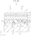
- Fig. 60 is a cross-sectional view illustrating the "rear surface illumination-type" solid-state imaging device.
- Fig. 61 shows a simulation result of a form of light traveling in the "rear surface illumination-type" solid-state imaging device.
- a result of a case where light having a wavelength of 650 nm vertically enters the surface of the silicon substrate 101J (3 ⁇ m thick) is shown.
- members such as on-chip lenses ML, color filters CF, and insulating films Z1, Z2 are provided on the rear surface side of the silicon substrate 101J.
- a wire layer 111 is provided on the front surface side of the silicon substrate 101J.
- the wire layer 111 is provided to cover a readout circuit (not shown) provided on the front surface side of the silicon substrate 101J.
- photodiodes provided inside the silicon substrate 101J sense light passing through the respective portions such as the on-chip lenses ML and the color filters CF. Further, the readout circuit (not shown) provided on the front surface side of the silicon substrate 101J reads out signal charges from the photodiodes (not shown).
- the light which enters the rear surface (the upper surface in Fig. 60 ) of the silicon substrate 101J through the respective portions such as the on-chip lenses ML and the color filters CF reaches the front surface (lower surface).
- light passing through the red filter layer CFR reaches the front surface of the silicon substrate 101J more than light passing through the green filter layer CFG, and 28% of the light reaches the front surface.
- the inventors of the present invention have recognized that even in the "rear surface illumination-type," the light coming from the rear surface side is not blocked and reaches the front surface side on which the accumulator is provided, and thus there are cases where noise is generated and image quality of a captured image is deteriorated.
- a solid-state imaging device includes a substrate and a photoelectric conversion region.
- the substrate has a charge accumulation region.
- the photoelectric conversion region is configured to generate signal charges to be accumulated in the charge accumulation region.
- the photoelectric conversion region is provided on the substrate.
- the photoelectric conversion region comprises a material that is not transparent (i.e. opaque).
- an electronic apparatus includes a solid-state imaging device.
- the solid state imaging device includes (a) a substrate, and (b) a photoelectric conversion region configured to generate signal charges.
- the photoelectric conversion region is provided on the substrate.
- the signal processing unit is configured to process an output of the solid-state imaging device.
- the photoelectric conversion region comprises a material that is not transparent (i.e. opaque).
- a method for manufacturing a solid-state imaging device includes forming a charge accumulation region in a substrate, and forming a photoelectric conversion region electrically connected to the charge accumulation region.
- the charge accumulation region is configured to accumulate signal charges generated by the photoelectric conversion region.
- the photoelectric conversion region comprises a material that is not transparent (i.e. opaque).
- the method may further comprise forming a transparent electrode on the photoelectric conversion region.
- the method may further comprise forming a layer having a first conductivity type on the photoelectric conversion region.
- the material may comprise a compound semiconductor having a chalcopyrite structure.
- the photoelectric conversion region may be formed by an epitaxial growth of the compound semiconductor.
- the method may further comprise forming a pixel dividing portion in the photoelectric conversion region by implanting impurities into a select portion of the photoelectric conversion region, wherein the pixel dividing portion forms a potential barrier in the photoelectric conversion region between adjacent pixels.
- the method may further comprise forming insulating regions interposed between the pixel dividing portion and the substrate.
- A-1 A configuration of main portions of a camera
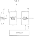
- Fig. 1 is a diagram illustrating a configuration of a camera 40 according to the first embodiment.
- the camera 40 includes a solid-state imaging device 1, an optical system 42, a control unit 43 (or controller 43), and a signal processing circuit 44. Each portion will be described sequentially.
- the solid-state imaging device 1 senses light (subject image) passing through the optical system 42 using an imaging surface PS and performs a photoelectric conversion for the light, thereby generating signal charges.
- the solid-state imaging device 1 is driven in response to a control signal output from the control unit 43. Specifically, the solid-state imaging device 1 reads out the signal charges and outputs the read-out signal charges as raw data.
- the optical system 42 includes optical members such as an imaging lens and a diaphragm, and is disposed so as to collect the incident light H which is incident as a subject image, on the imaging surface PS of the solid-state imaging device 1.
- the control unit 43 outputs various kinds of control signals to the solid-state imaging device 1 and the signal processing circuit 44 so as to control and drive the solid-state imaging device 1 and the signal processing circuit 44.
- the signal processing circuit 44 performs a signal process for an electric signal output from the solid-state imaging device 1 and thus generates a digital image of a subject image.
- A-2 A configuration of main portions of the solid-state imaging device
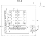
- Fig. 2 is a block diagram illustrating the entire configuration of the solid-state imaging device 1 according to the first embodiment.
- the solid-state imaging device 1 is constituted by, for example, a CMOS type image sensor.
- the solid-state imaging device 1 includes a silicon substrate 11 as shown in Fig. 2 .
- the silicon substrate 11 is a semiconductor substrate made of, for example, a monocrystalline silicon semiconductor, and has an imaging area PA and a peripheral area SA on its surface, as shown in Fig. 2 .
- the imaging area PA has a rectangular shape as shown in Fig. 2 , wherein plural pixels P are respectively arranged in the horizontal direction x and the vertical direction y. In other words, the pixels P are arranged in a matrix.
- the imaging area PA corresponds to the imaging surface PS shown in Fig. 1 . Details of the pixels P will be described later.
- the peripheral area SA is positioned around the imaging area PA as shown in Fig. 2 . Further, peripheral circuits are provided in the peripheral area SA.
- a vertical driving circuit 3 As the peripheral circuits, a vertical driving circuit 3, a column circuit 4, a horizontal driving circuit 5, an outward output circuit 7, and a timing generator 8 are provided.
- the vertical driving circuit 3, as shown in Fig. 2 is provided in the side part of the imaging area PA in the peripheral area SA, and is electrically connected to the respective rows of the plural pixels P arranged in the horizontal direction H in the imaging area PA.
- the column circuit 4 as shown in Fig. 2 , is provided in the lower part of the imaging area PA in the peripheral area SA, and performs signal processes for signals output from the pixels P with column units.
- the column circuit 4 includes a CDS (correlated double sampling) circuit (not shown), and performs a signal process for removing fixed pattern noise.
- CDS correlated double sampling
- the horizontal driving circuit 5 is electrically connected to the column circuit 4 as shown in Fig. 2 .
- the horizontal driving circuit 5 includes, for example, shift registers, and sequentially outputs the signals for each column of the pixels P, which are held in the column circuit 4, to the outward output circuit 7.
- the outward output circuit 7, as shown in Fig. 2 is electrically connected to the column circuit 4, and performs a signal process for the signals output from the column circuit 4, and then outputs the processed signals to an external device.
- the outward output circuit 7 includes an AGC (automatic gain control) circuit 7a and an ADC (analog-to-digital conversion) circuit 7b.
- the AGC circuit 7a gives a gain to the signals and then the ADC circuit 7b converts the analog signals to digital signals for output to the external device.
- the timing generator 8 as shown in Fig. 2 , is electrically connected to the vertical driving circuit 3, the column circuit 4, the horizontal driving circuit 5, and the outward output circuit 7.
- the timing generator 8 generates various kinds of pulse signals, and outputs the pulse signals to the respective portions of the vertical driving circuit 3, the column circuit 4, the horizontal driving circuit 5, and the outward output circuit 7 for driving control.
- Figs. 3 and 4 are diagrams illustrating main portions of the solid-state imaging device according to the first embodiment.
- Fig. 3 shows a cross-section of the pixels P.
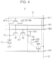
- Fig. 4 shows a circuit configuration of the pixel P.
- the solid-state imaging device 1 includes the silicon substrate 11, and a photoelectric conversion film 13 is formed on one side surface (upper surface) of the silicon substrate 11.
- a photoelectric conversion film 13 is formed on one side surface (upper surface) of the silicon substrate 11.
- on-chip lenses ML and color filters CF are provided on the silicon substrate 11.
- a gate MOS 41 is provided on the other side surface (lower surface) of the silicon substrate 11, as shown in Fig. 3 .
- independent gate MOS 42 and a readout circuit 51 are provided as shown in Fig. 4 .
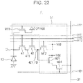
- the readout circuit 51 includes a PD reset transistor M11, an amplification transistor M21, and a selection transistor M31.
- a wire layer (not shown) is provided on the other side surface (lower surface) of the silicon substrate 11 so as to cover the respective portions such as the gate MOS 41.
- the photoelectric conversion film 13 senses the incident light H passing through the on-chip lenses ML and the color filters CF from the rear surface (upper surface) side and generates signal charges.
- the signal charges generated by the photoelectric conversion film 13 are accumulated in an n-type impurity area 12 provided in the silicon substrate 11. Thereafter, the signal charges accumulated in the n-type impurity area 12 is transferred to an n-type impurity region 411 by the gate MOS 41 and are accumulated in the n-type impurity region 411. Also, the signal charges are transferred by the gate MOS 42 and read out by the readout circuit 51, and then output to the vertical signal line 27 as electric signals.
- the solid-state imaging device 1 is constituted by a "rear surface illumination-type CMOS image sensor.”
- the photoelectric conversion film 13 As shown in Fig. 3 , is provided on the one side surface (upper surface) of the silicon substrate 11 which is, for example, a p-type silicon semiconductor.
- the photoelectric conversion film 13 is formed as a single body over the plural pixels P, as shown in Figs. 2-3 .
- the photoelectric conversion film 13 is provided to cover the n-type impurity areas 12 which are formed to correspond to the plural pixels P in the silicon substrate 11. As illustrated, the photoelectric conversion film 13 is adjacent to, in contact with, and/or in direct contact with the n-type impurity areas.
- Each of the n-type impurity areas 12 functions as an accumulator which accumulates the signal charges generated by the photoelectric conversion film 13.
- the impurity is preferably distributed such that concentration of the impurity increases from the upper surface to the lower surface of the silicon substrate. In this way, the signal charges (here, electrons) moved from the photoelectric conversion film 13 can be naturally moved to the gate MOS 41 side in the n-type impurity area 12.
- a transparent electrode 14 is provided on the photoelectric conversion film 13.
- the transparent electrode 14 is connected to the ground, and thus prevents charging due to the accumulation of holes.
- the photoelectric conversion film 13 is interposed between the n-type impurity area 12 functioning as a lower electrode and the transparent electrode 14 functioning as an upper electrode.
- the photoelectric conversion film 13 senses the incident light H and performs photoelectric conversion for the light in the respective pixels P, thereby generating signal charges.
- the photoelectric conversion film 13 has an anode connected to the ground, and the accumulated signal charges (here, electrons) are read out through the gate MOS 41, the gate MOS 42 and the readout circuit 51, and output to the vertical signal line 27 as electric signals.
- the accumulated signal charges here, electrons
- the photoelectric conversion film 13 is connected to a gate of the amplification transistor M21 via the gate MOS 41 and the gate MOS 42, as shown in Fig. 4 . Further, in the photoelectric conversion film 13, the accumulated signal charges are transferred to a floating diffusion FD connected to the gate of the amplification transistor M21, by the gate MOS 41 and the gate MOS 42 as output signals.
- the photoelectric conversion film 13 functions as the accumulator which accumulates the signal charges like the n-type impurity area 12 and as a light blocking film which blocks the incident light H from reaching the accumulator, in addition to perform the photoelectric conversion. Along therewith, the photoelectric conversion film 13 functions as a light blocking film which blocks the incident light H which travels towards the readout circuit 51, from reaching the readout circuit 51.
- the photoelectric conversion film 13 is made of a compound semiconductor having a chalcopyrite structure.
- the photoelectric conversion film 13 is made of CuInSe 2 which is the compound semiconductor having the chalcopyrite structure.
- Fig. 5 is a diagram illustrating a relationship between photon energy and a light absorption coefficient.
- CuInSe 2 is higher than other materials in the light absorption coefficient, and particularly, is double digits higher than the Si single crystal (in the figure, x-Si). For this reason, CuInSe 2 suitably functions not only as a photoelectric conversion film but also as a light blocking film which blocks visible light.
- the photoelectric conversion film 13 may use materials having any crystal structure such as monocrystalline, polycrystalline or amorphous structures as long as the materials have the higher absorption coefficient of visible light than the silicon substrate 11 and realize the photoelectric conversion function.
- the photoelectric conversion film 13 may be formed using chalcopyrite materials other than CuInSe 2 .
- Figs. 6 and 7 are diagrams illustrating a relationship between a lattice constant and a band gap regarding the chalcopyrite materials.
- the photoelectric conversion film 13 may be made of a compound semiconductor with the chalcopyrite structure including copper-aluminum-gallium-indium-sulfur-selenium based mixed crystal.
- the copper-aluminum-gallium-indium-sulfur-selenium based mixed crystal can be formed through the control of the composition so as to correspond with the lattice constant of silicon (Si), and thus a crystal defect can be reduced.
- the copper-aluminum-gallium-indium-sulfur-selenium based mixed crystal can be epitaxially grown on the silicon substrate 11 as a monocrystalline thin film, and thus a crystal defect such as a misfit dislocation occurring at a heterointerface, it is possible to suppress generation of dark currents and reduce noise.
- the photoelectric conversion film 13 may be formed using a compound semiconductor with the chalcopyrite structure including a copper-aluminum-gallium-indium-zinc-sulfur-selenium based mixed crystal.
- Fig. 8 is a diagram illustrating a band structure of the solid-state imaging device according to the first embodiment.
- Fig. 8 shows a band structure for parts of the photoelectric conversion film 13 and the silicon substrate 11. In other words, a band structure in the depth direction z of the photoelectric conversion film 13 and the silicon substrate 11 is shown.
- the band is formed to be tilted with respect to the photoelectric conversion film 13. Due to this, accumulated electrons are easily moved to the silicon substrate 11 side.
- the conductivity type of the photoelectric conversion film 13 is, for example, a p-type.
- the photoelectric conversion film 13 may be of an i type or an n-type, in addition to the p-type.
- the gate MOS 41 and the gate MOS 42 are provided for each of the plural pixels P shown in Fig. 2 , as shown in Fig. 4 .
- the gate MOS 41 and the gate MOS 42 output the generated signal charges to the gate of the amplification transistor M21 as the electric signals.
- the gate MOS 41 and the gate MOS 42 as shown in Fig. 4 , are provided to be interposed between the photoelectric conversion film 13 and the floating diffusion FD.
- the gate MOS 41 and the gate MOS 42 transfer the signal charges to the floating diffusion FD as output signals when the gates are applied with readout signals from the readout lines H41 and H42.
- the gate MOS 41 is provided on the opposite surface (front surface) side to the surface (rear surface) on which the photoelectric conversion film 13 is provided in the silicon substrate 11, as shown in Fig. 3 .
- the gate MOS 42 is provided on the opposite surface (front surface) side to the surface (rear surface) on which the photoelectric conversion film 13 is provided in the silicon substrate 11.
- the gate MOS 41 and the gate MOS 42 have active areas (not shown) formed in the silicon substrate 11, and the gates thereof are made of conductive materials.
- the readout circuits 51 are disposed in plurality so as to correspond to the plural pixels P shown in Fig. 2 .
- the readout circuit 51 includes the PD reset transistor M11, the amplification transistor M21, and the selection transistor M31, and reads out the signal charges through the gate MOS 41.
- the respective transistors M11, M21 and M31 constituting the readout circuit 51 is provided on the opposite surface (front surface) side to the surface (rear surface) on which the photoelectric conversion film 13 is provided in the silicon substrate 11.
- the respective transistors M11, M21 and M31 have, for example, active areas (not shown) formed in the silicon substrate 11, and the gates thereof are made of conductive materials.
- the PD reset transistor M11 resets a potential at the photoelectric conversion film 13.
- the PD reset transistor M11 has a gate connected to a PD reset line H11 which is supplied with a PD reset signal.
- the PD reset transistor M11 is electrically connected to the photodiode which has one terminal connected to the ground and the other terminal which is formed of the photoelectric conversion film 13.
- the PD reset transistor M11 resets a potential at the photodiode in response to the PD reset signal output from the PD reset line H11.
- the amplification transistor M21 amplifies and outputs the electric signals resulting from the signal charges.
- the amplification transistor M21 has a gate connected to the floating diffusion FD.
- the amplification transistor M21 has a drain connected to a power source potential supply line Vdd, and a source connected to the selection transistor M31.
- the amplification transistor M21 is supplied with a constant current from a constant current source (not shown) when the selection transistor M31 is turned on, and thus works as a source follower. For this reason, the amplification transistor M21 amplifies the output signals from the floating diffusion FD when the selection signal is supplied to the selection transistor M31.
- the selection transistor M31 outputs the electric signals output from the amplification transistor M21 to the vertical signal line 27 when the selection signal is input to the selection transistor M31.
- the selection transistor M31 has a gate connected to a selection line H31 which is supplied with the selection signal.
- the selection transistor M31 is turned on when the selection signal is supplied, and outputs the output signals amplified by the amplification transistor M21 to the vertical signal line 27 as described above.
- the color filter CF and the on-chip lens ML are provided on the upper surface (rear surface) side of the silicon substrate 11 so as to correspond to the pixel P.
- the color filter CF includes filters of the three primary colors, for example, a red filter layer (not shown), a green filter layer (not shown), and a blue filter layer (not shown). Further, the filters of the three primary colors are disposed for each pixel P, for example, in the Bayer arrangement.
- the arrangement of the filter layers of the respective colors is not limited to the Bayer arrangement, but may be other arrangements.
- the on-chip lens ML is provided over the upper surface of the silicon substrate 11 via the photoelectric conversion film 13, the transparent electrode 14, and the color filter CF.
- the on-chip lens ML is provided to protrude upwards in the convex shape from the silicon substrate 11, and collects the incident light H coming from above on the photoelectric conversion film 13.
- the wire layer (not shown) is provided on the lower surface (front surface) of the silicon substrate 11 to cover the respective portions such as the gate MOS 41.
- a wire (not shown) electrically connected to each circuit element is formed inside an insulating layer (not shown).
- the respective wires constituting the wire layer are laminated and formed so as to function as a wire such as the readout line H41 shown in Fig. 4 .
- Figs. 9A and 9B are diagrams illustrating a manufacturing method of the solid-state imaging device according to the first embodiment.
- FIGS. 9A and 9B show the cross-sections in the same manner as Fig. 3 , and the solid-state imaging device 1 shown in Fig. 3 is manufactured through the respective steps shown in Figs. 9A and 9B .
- the photoelectric conversion film 13 is formed as shown in Fig. 9A .
- the respective portions such as the gate MOS 41 are formed on the surface of the silicon substrate 11 before the photoelectric conversion film 13 is formed. Further, the wire layer (not shown) is formed on the surface (front surface) of the silicon substrate 11 so as to cover the respective portions such as the gate MOS 41.
- the respective portions are formed on a silicon layer of a so-called SOI substrate (corresponding to the silicon substrate 11), and then the silicon layer is transcribed onto a surface of another glass substrate (not shown). Thereby, the rear surface side of the silicon substrate 11 which is the silicon layer is seen and the (100) surface is exposed.
- the n-type impurity area 12 is formed inside or within a portion of the silicon substrate 11.
- the photoelectric conversion film 13 is formed on the opposite surface (rear surface) to the surface on which the respective portions such as the gate MOS 41 are formed in the silicon substrate 11.
- the photoelectric conversion film 13 is made of the compound semiconductor with the chalcopyrite structure including, for example, CuInSe 2 mixed crystal.
- a compound semiconductor with the chalcopyrite structure including copper-aluminum-gallium-indium-sulfur-selenium based mixed crystal may be formed on the silicon substrate 11 so as to lattice-match with the silicon substrate 11, thereby forming the photoelectric conversion film 13.
- the compound semiconductor is epitaxially grown on the silicon substrate 11 by, for example, an MBE method, an MOCVD method, or the like, thereby forming the photoelectric conversion film 13.
- the lattice constant of silicon (Si) is 5.431 ⁇ .
- the CuAlGaInSSe based mixed crystal includes a material corresponding to the lattice constant, and can be formed so as to lattice-match with the silicon substrate 11. Thereby, for example, a CuGa 0.52 In 0.48 S 2 film is formed on the silicon substrate 11 as the photoelectric conversion film 13.
- the photoelectric conversion film 13 is formed so as to have, for example, a p-type as a conductivity type. In addition to the p-type, the photoelectric conversion film 13 may be formed to have an i type or an n-type as the conductivity type.
- the p-type CuGa 0.52 In 0.48 S 2 film is formed and then the photoelectric conversion film 13 is formed such that, for example, concentration of zinc (Zn) which is an n-type impurity is reduced according to the crystal growth.
- the photoelectric conversion film 13 can be formed such that the band is tilted in the depth direction z.
- the photoelectric conversion film 13 is formed such that the concentration of the impurity becomes, for example, 10 14 to 10 16 cm -3 . In addition, the photoelectric conversion film 13 is formed such that the film thickness becomes 300 nm.
- the photoelectric conversion film 13 is formed to cover parts where pixel dividing portions PB are formed on the silicon substrate by epitaxially growing the compound semiconductor.
- the photoelectric conversion film 13 can be formed such that the band is tilted in the depth direction z as in the above description.
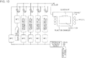
- Fig. 10 is a diagram illustrating an MOCVD device used in the first embodiment.
- the MOCVD device shown in Fig. 10 is used.
- the substrate can be placed on a susceptor (made of carbon) as shown in Fig. 10 .
- the susceptor is heated by a high frequency heating device (RF coils), and a temperature of the substrate is controlled.
- RF coils high frequency heating device
- the substrate is heated in a temperature range of 400°C to 1000°C where thermal decomposition can occur.
- organic metal raw-materials are bubbled by hydrogen to enter a saturated vapor pressure state, and each raw-material molecule is transferred to a reaction tube.
- a flow rate of hydrogen which flows towards each raw-material due to a mass flow controller (MFC) is controlled, and a molar amount of the raw-material which is transferred per unit of time is adjusted.
- the organic metal raw-materials are thermally decomposed on the substrate and grow the crystal. There is a correlation between a ratio of transferred molar amount and a composition ratio of the crystal. Thereby, the composition ratio of the crystal can be arbitrarily adjusted.
- the following organic metals may be used.
- organic metal of copper for example, acetylacetone copper (Cu(C 5 H 7 O 2 ) 2 ) is used.
- cyclopentadienyl copper triethylene h5-(C 2 H 5 )Cu:P(C 2 H 5 ) 3 ) may be used.
- Ga gallium
- trimethyl gallium Ga(CH 3 ) 3
- triethyl gallium Ga(C 2 H 5 ) 3
- Al an organic metal of aluminum
- Al(CH 3 ) 3 trimethyl aluminum
- Al(C 2 H 5 ) 3 triethyl aluminum
- indium for example, trimethyl indium (In(CH 3 ) 3 )is used.
- triethyl indium (In(C 2 H 5 ) 3 ) may be used.
- organic metal of selenium for example, dimethyl selenium (Se(CH 3 ) 2 )is used.
- diethyl selenium (Se(C 2 H 5 ) 2 ) may be used.
- organic metal of sulfur for example, dimethyl sulfide (S(CH 3 ) 3 ) is used.
- diethyl sulfide S(C 2 H 5 ) 2 ) may be used.
- Zn dimethyl zinc (Zn(CH 3 ) 2 )is used.
- diethyl zinc (Zn(C 2 H 5 ) 2 ) may be used.
- H 2 Se hydrogen selenide
- S raw-material hydrogen sulfide
- the raw-material such as cyclopentadienyl copper triethylene (h5-(C 2 H 5 )Cu:P(C 2 H 5 ) 3 ), acetylacetone copper (Cu(C 5 H 7 O 2 ) 2 ) or trimethyl indium (In(CH 3 ) 3 ) is in a solid phase state at room temperature. In this case, the raw-material enters a liquid phase state through heating. In addition, even in the solid phase state, the raw-material may be used in a high vapor pressure simply at a high temperature.
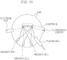
- Fig. 11 is a diagram illustrating an MBE device used in the first embodiment.
- the MBE device shown in Fig. 11 is used.
- the simple substance raw-material of copper, and each of the simple substance raw-materials of gallium (Ga), aluminum (Al), indium (In), selenium (Se), and sulfur (S) are contained in each Knudsen cell. Further, these raw-materials are heated at an appropriate temperature, and the substrate is irradiated with each of molecular beams so as to perform crystal growth.
- a portion of raw-materials may use gas sources.
- a Se material hydrogen selenide (H 2 SE) may be used, and, as a sulfur (S) raw-material, hydrogen sulfide (H 2 S) may be used.
- the transparent electrode 14 is formed as shown in Fig. 9B .
- the transparent electrode 14 is formed to cover the upper surface of the photoelectric conversion film 13.
- the transparent electrode 14 is made of indium tin oxide (ITO).
- the transparent electrode 14 may be made of a transparent conductive material such as zinc oxide or indium zinc oxide.
- the transparent electrode 14 is formed as a single body over the plural pixels P shown in Fig. 2 .
- the respective portions such as the color filters CF and the on-chip lenses ML are formed on the upper surface (rear surface) of the silicon substrate 11. In this way, the rear surface illumination-type CMOS image sensor is completed.
- Figs. 12 to 13E are diagrams illustrating an operation of the solid-state imaging device 1 according to the first embodiment.
- Fig. 12 is a cross-sectional view and shows movements of electrons or holes when the incident light H enters the photoelectric conversion film 13.
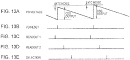
- Figs. 13A to 13E show timing charts.
- Fig. 13A indicates a voltage at the photodiode constituted by the photoelectric conversion film 13 (refer to Fig. 4 ).
- Fig. 13B indicates a PD reset signal transmitted to the gate of the PD reset transistor M11 via the PD reset line H11.
- Fig. 13C indicates a first readout signal transmitted to the gate of the gate MOS 41 via the readout line H41.
- Fig. 13D indicates a second readout signal transmitted to the gate of the gate MOS 42 via the readout line H42.
- Fig. 13E indicates a selection signal transmitted to the gate of the selection transistor M31 via the selection line H31.
- Figs. 13A to 13E shows that the signals have a high level at the longitudinal lines extending vertically from the transverse lines, and thus the respective transistors are turned on.
- the global exposure is performed in which the incident light is sensed by all the pixels P at the same time, and then the sensing is finished without using a mechanical light blocking unit. That is to say, the exposure is performed by the "global shutter method.”
- the incident light H enters the photoelectric conversion film 13 passing through the respective portions from the upper side of the silicon substrate 11.
- the generated electrons are moved to the n-type impurity area 12 (accumulator 1) of the silicon substrate 11, and the holes are moved to the transparent electrode 14.
- the signal charges accumulated in the n-type impurity area 12 (accumulator 1) are transferred to the n-type impurity region 411 (accumulator 2) by the gate MOS 41, and immediately thereafter, PD reset is made.
- the n-type impurity area 12 (accumulator 1) is connected to the ground by the PD reset transistor M11, and the potential is reset to the voltage 0V (or, the power source voltage Vdd) (refer to Fig. 4 ).
- the signal charges begin to accumulate.
- the signal charges are transferred to the n-type impurity region 421 (FD) by the gate MOS 42 and then accumulated.
- the readout circuit 51 reads out the signal charges for each pixel P and outputs the read-out signal charges to the vertical signal line 27 as electric signals.
- the fixed pattern noise in the amplification transistor M21 can be removed through the subtraction between the signals before and after the reset by the CDS circuit.
- the PD reset is made immediately after the signal charges accumulated in the n-type impurity area 12 (accumulator 1) are transferred to the n-type impurity region 411 (accumulator 2). For this reason, a variation in the reset signal voltage which is used as a reference when the CDS process is performed occurs, and thus kTC noise is included.
- the photoelectric conversion film 13 functions as a light blocking film along with the photoelectric conversion function.
- the incident light H is blocked from entering the respective n-type impurity areas 12 and 411, which function as the accumulators, by the photoelectric conversion film 13.
- the incident light H is blocked from entering the readout circuit 51 or the n-type impurity region 421 (floating diffusion layer) which functions as a floating diffusion by the photoelectric conversion film 13.
- Fig. 14 is a diagram illustrating a simulation result of a form of light traveling in the solid-state imaging device according to the first embodiment.
- a result is shown when light having the wavelength of 650 nm enters a CuInGaS 2 film with the thickness of 0.3 ⁇ m which is formed as the photoelectric conversion film 13 on the silicon substrate 11 (0.5 ⁇ m thick) as in Fig. 60 .
- the incident light is absorbed and blocked by the photoelectric conversion film 13 and thus does not enter the silicon substrate 11.
- a rate of light reaching the bottom of the silicon substrate 11 is specifically estimated, only the light of 1.8x10 -3 % reaches, and the light is nearly blocked.
- the photoelectric conversion film 13 in the pixels P, the photoelectric conversion film 13 generates the signal charges by sensing and photoelectric-converting the incident light H.
- the signal charges generated by the photoelectric conversion film 13 are read out by the readout circuit 51.
- the signal charges generated by the photoelectric conversion film 13 are accumulated in the n-type impurity areas 12 and 411 which are the accumulators.
- the photoelectric conversion film 13 is provided at the side where the incident light H enters when seen from the readout circuit 51 and the n-type impurity areas 12 and 411 in the silicon substrate 11, and thus blocks the incident light H from entering the readout circuit 51 and the n-type impurity areas 12 and 411.
- the pixels P include the photoelectric conversion film 13, and the photoelectric conversion film 13 is made of the compound semiconductor having the chalcopyrite structure.
- the photoelectric conversion film 13 is formed on the silicon substrate 11 so as to lattice-match with the silicon substrate 11.
- the crystallinity of the photoelectric conversion film 13 is improved.
- the crystal defect is reduced, and thereby it is possible to suppress the generation of a dark current and prevent deterioration of the image quality due to white dots.
- a high quality imaging can be performed even in a dark imaging environment (for example, night time).
- the definition of the "lattice matching" includes a state close to the lattice matching under a condition of the thickness of the photoelectric conversion film being within a critical film thickness.
- the thickness is within the critical film thickness, the lattice matching is not completely made, but the crystallinity can become good since the misfit dislocation is not included.
- the "critical film thickness” is defined by the equation (1) by "Matthews and Blakeslee” (for example, refer to J. W. Mathews and A. E. Blakeslee, J. Cryst. Growth 27(1974) 118-125 ) and the equation (2) by "People and Bean” (for example, refer to R. People and J. C. Bean, Appl. Phys. Lett. 47(1985) 322-324 ).
- a denotes a lattice constant
- b denotes a Burgers vector for dislocation
- v denotes a Poisson ratio
- f denotes a lattice mismatching
- h c b 2 ⁇ f 1 1 + v ln h c b + 1 h c 1 16 ⁇ 2 1 ⁇ v 1 + v b 2 a 1 f 2 ln h c b
- the photoelectric conversion film 13 is made of the chalcopyrite materials
- the present invention is not limited thereto.
- the photoelectric conversion film 13 may be made of silicide based materials.
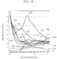
- Fig. 15 is a diagram illustrating a relationship between the photon energy (eV) and the absorption index k in the silicide materials.
- the silicide based materials such as CoSi, CrSi, HfSi, IrSi, MoSi, NiSi, PdSi, ReSi, TaSi, TiSi, WSi, and ZrSi have a higher light absorption coefficient ⁇ than Si.
- ⁇ -iron silicide material ( ⁇ -FeSi 2 ) is double digits higher than Si in the light absorption coefficient (refer to H. Katsumata, et al., J. Appl. Phys. 80 (10), 5955 (1996 )).
- the ⁇ -iron silicide material ( ⁇ -FeSi 2 ) can be epitaxially grown on a silicon substrate (refer to John E. Mahan, et al., Appl. Phys. Lett. 56 (21), 2126 (1990 )).
- the photoelectric conversion film 13 can be formed so as to realize both the photoelectric conversion function and the light blocking function by using the ⁇ -iron silicide material ( ⁇ -FeSi 2 ).
- a Barium silicide based material (BaSi 2 ) or Ba 1 - x Sr x Si 2 is about double digits higher than silicon (Si) in the light absorption coefficient (refer to the following reference).
- silicide materials such as SiGe, Mg 2 SiGe, SrSi 2 , MnSi 17 , CrSi 2 , Ni-Si, Cu/Si, Co/Si, or Pt/Si are higher than Si in the light absorption coefficient.
- the photoelectric conversion film 13 can be formed so as to also function as a light blocking film by using silicide materials.
- the photoelectric conversion film 13 may be formed using organic materials.
- quinacridone or coumarin based organic materials, or the like have the light absorption coefficient almost twice higher than Si, and the photoelectric conversion film 13 can be formed so as to have the light blocking function along with the photoelectric conversion function by using them.
- the kTC noise is included in the signal, but the kTC noise may be removed as described below.
- Fig. 16 is a diagram illustrating a circuit configuration of a pixel constituting a solid-state imaging device according to a modified example 1-2 of the first embodiment.
- Figs. 17 to 18F are diagrams illustrating an operation of the solid-state imaging device according to the modified example 1-2 of the first embodiment.
- Fig. 17 is a cross-sectional view in the same manner as Fig. 12 , and shows movements of electrons or holes when the incident light H enters the photoelectric conversion film 13.
- Figs. 18A to 18F show timing charts in the same manner as Figs. 13A to 13E .
- Fig. 18A indicates a voltage at the photodiode constituted by the photoelectric conversion film 13 (refer to Fig. 16 ).
- Fig. 18B indicates a voltage at the n-type impurity region 411 which functions as a floating diffusion.
- Fig. 18C indicates a PD reset signal transmitted to the gate of the PD reset transistor M11 via the PD reset line H11.
- Fig. 18D indicates an FD reset signal transmitted to a gate of an FD reset transistor M12 via an FD reset line H12.
- Fig. 18A indicates a voltage at the photodiode constituted by the photoelectric conversion film 13 (refer to Fig. 16 ).
- Fig. 18B indicates a voltage at the n-type impurity region 411 which functions as a floating diffusion.
- Fig. 18C indicates a PD reset signal transmitted to the gate of the PD
- Fig. 18E indicates a readout signal transmitted to the gate of the gate MOS 41 via the readout line H41.
- Fig. 18F indicates a selection signal transmitted to the gate of the selection transistor M31 via the selection line H31.
- Figs. 18A to 18F shows that the signals have a high level at the longitudinal lines extending vertically from the transverse lines, and thus the respective transistors are turned on.
- the FD reset transistor M12 which resets a potential at the floating diffusion FD may be provided instead of the gate MOS 42 (refer to Fig. 4 ) in the first embodiment.
- the FD reset transistor M12 has the gate connected to the FD reset line H12 which is supplied with the FD reset signal. Further, the FD reset transistor M12 has one terminal connected to the floating diffusion FD (n-type impurity region 411) and the other terminal electrically connected to the power source potential supply line Vdd. Also, the FD reset transistor M12 resets a potential at the floating diffusion FD (n-type impurity region 411) in response to the FD reset signal output from the FD reset line H12.
- the incident light H enters the photoelectric conversion film 13 passing through the respective portions from the upper side of the silicon substrate 11.
- the generated electrons are moved to the n-type impurity area 12 (accumulator 1) of the silicon substrate 11, and the holes are moved to the transparent electrode 14.
- the photoinduced charges generated by the photoelectric conversion film 13 are moved to the surface opposite to the light incident surface since an internal electric field generated by a doping control exists in the n-type impurity area 12 (accumulator 1) of the silicon substrate 11.
- a potential at the n-type impurity area 12 (accumulator 1) is reset to 0V or the power source voltage Vdd (V) through the "PD reset" (here, the case where reset to Vdd (V) is shown).
- the signal charges begin to accumulate.
- the potential at the n-type impurity area 12 (accumulator 1) is reset by the PD reset transistor M11 as shown in Figs. 18A to 18F , the electrons (signal charges) begin to accumulate.
- the signal charges accumulated in the n-type impurity area 12 are transferred to the n-type impurity region 411 (accumulator 2) by the gate MOS 41 and then accumulated.
- the readout circuit 51 reads out the signal charges and outputs the read-out signal charges to the vertical signal line 27 as electric signals.
- This operation is performed in all the pixels P.
- the selection transistor M31 is turned on using the selection line H31 for each pixel P or each row of the pixels P, a voltage variation in the n-type impurity region 411 (accumulator 2 also used as FD)is amplified by the amplification transistor M21, and then the signals are sequentially read out.
- the PD voltage drops due to the accumulation of the signal charges.
- a variation in the voltage occurs when the "PD reset" or the "FD reset” is made, and thus the kTC noise is generated.
- the variation is removed through the correlated double sampling (CDS) process and thus the kTC can be removed.
- the noise can be removed with a difference between the pixel signal voltage and the reset signal voltage (CDS operation).
- the n-type impurity region 411 (according to 2 also used as FD) comes into direct contact with the surface of the silicon substrate 11, a dark current is generated at a surface level.
- the photoelectric conversion film 13 functions as a light blocking film along with the photoelectric conversion function. Thereby, as shown in Fig. 17 , the incident light H is blocked from entering the respective n-type impurity areas 12 and 411, which function as the accumulators, by the photoelectric conversion film 13.
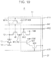
- Fig. 19 is a diagram illustrating a circuit configuration of a pixel constituting a solid-state imaging device according to a modified example 1-3 of the first embodiment.
- Figs. 20 to 21G are diagrams illustrating an operation of the solid-state imaging device according to the modified example 1-3 of the first embodiment.
- Fig. 20 is a cross-sectional view in the same manner as Fig. 17 , and shows movements of electrons or holes when the incident light H enters the photoelectric conversion film 13.
- Figs. 21A to 21G are diagrams illustrating an operation of the solid-state imaging device according to the modified example 1-3 of the first embodiment.
- Figs. 21A to 21G show timing charts.
- Fig. 21A indicates a voltage at the photodiode constituted by the photoelectric conversion film 13 (refer to Fig. 20 ).
- Fig. 21B indicates a voltage at the n-type impurity region 411 which functions as a floating diffusion.
- Fig. 21C indicates a PD reset signal transmitted to the gate of the PD reset transistor M11 via the PD reset line H11.
- Fig. 21D indicates an FD reset signal transmitted to a gate of an FD reset transistor M12 via an FD reset line H12.
- Fig. 21A indicates a voltage at the photodiode constituted by the photoelectric conversion film 13 (refer to Fig. 20 ).
- Fig. 21B indicates a voltage at the n-type impurity region 411 which functions as a floating diffusion.
- Fig. 21E indicates a signal (transparent electrode) transmitted to the transparent electrode 14.
- Fig. 21F indicates a readout signal transmitted to the gate of the gate MOS 41 via the readout line H41.
- Fig. 21G indicates a selection signal transmitted to the gate of the selection transistor M31 via the selection line H31.
- Figs. 21A to 21G show that the signals have a high level at the longitudinal lines extending vertically from the transverse lines, and thus the respective transistors are turned on.
- Fig. 21E shows the signal (transparent electrode) transmitted to the transparent electrode 14 in addition to the signals shown in Figs. 18A to 18F .
- the modified example 1-2 of the first embodiment may be configured to apply a signal to the transparent electrode 14 so as to control the potential. Due to this, even in a case where there is a single accumulator, the exposure by the global shutter method can be performed.
- a signal of a zero bias or a negative bias is applied to the transparent electrode 14.
- the generated photoinduced charges are moved to the n-type impurity area 12 (accumulator 1) and then begin to be accumulated.
- a positive bias is applied to the transparent electrode 14. Therefore, newly generated photoinduced charges are moved to the transparent electrode 14 side, and the accumulation in the n-type impurity area 12 (accumulator 1) is finished.
- the photoinduced charges are transferred to the n-type impurity region 411 (FD) using the readout line H41. Further, immediately thereafter, using the selection line H31 for each pixel P or each row of the pixels P, a voltage variation in the n-type impurity region 411 (FD) is amplified by the amplification transistor M21, and then a signal thereof is read out. This is sequentially repeated.
- the kTC noise can be removed by reading out a difference between the pixel signal voltage and the reset signal voltage as a signal using the CDS circuit. This structure is effective for a fine pixel since the number of transistors necessary for each pixel is reduced.
- n-type impurity region 411 (accumulator 2 also used as FD) comes into direct contact with the surface of the silicon substrate 11, a dark current is generated at a surface level.
- Fig. 22 is a diagram illustrating a circuit configuration of a pixel constituting a solid-state imaging device according to a modified example 1-4 of the first embodiment.
- Figs. 23 to 24G are diagrams illustrating an operation of the solid-state imaging device according to the modified example 1-4 of the first embodiment.
- Fig. 23 is a cross-sectional view in the same manner as Fig. 12 , and shows movements of electrons or holes when the incident light H enters the photoelectric conversion film 13.
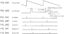
- Figs. 24A to 24G show timing charts in the same manner as Figs. 13A to 13E .
- Fig. 24A indicates a voltage at the photodiode constituted by the photoelectric conversion film 13 (refer to Fig. 22 ).
- Fig. 24B indicates a voltage at the n-type impurity region 421 which functions as a floating diffusion.
- Fig. 24C indicates a PD reset signal transmitted to the gate of the PD reset transistor M11 via the PD reset line H11.
- Fig. 24D indicates an FD reset signal transmitted to a gate of an FD reset transistor M 12 via an FD reset line H12.
- Fig. 24A indicates a voltage at the photodiode constituted by the photoelectric conversion film 13 (refer to Fig. 22 ).
- Fig. 24B indicates a voltage at the n-type impurity region 421 which functions as a floating diffusion.
- Fig. 24C indicates a PD reset signal transmitted to the gate of the PD
- Fig. 24E indicates a first readout signal transmitted to the gate of the gate MOS 41 via the readout line H41.
- Fig. 24F indicates a second readout signal transmitted to the gate of the gate MOS 42 via the readout line H42.
- Fig. 24G indicates a selection signal transmitted to the gate of the selection transistor M31 via the selection line H31.
- Figs. 24A to 24G shows that the signals have a high level at the longitudinal lines extending vertically from the transverse lines, and thus the respective transistors are turned on.
- the FD reset transistor M12 described in the modified example 1-2 may be added to the configuration according to the first embodiment.
- the FD reset transistor M12 has the gate connected to the FD reset line H12 which is supplied with the FD reset signal. Further, the FD reset transistor M12 has one terminal connected to the floating diffusion FD (n-type impurity region 421) and the other terminal electrically connected to the power source potential supply line Vdd. Also, the FD reset transistor M12 resets a potential at the floating diffusion FD (n-type impurity region 421) in response to the FD reset signal output from the FD reset line H12.
- the incident light H enters the photoelectric conversion film 13 passing through the respective portions from the upper side of the silicon substrate 11.
- the generated electrons are moved to the n-type impurity area 12 (accumulator 1) of the silicon substrate 11, and the holes are moved to the transparent electrode 14.
- a potential at the n-type impurity area 12 (accumulator 1) is reset to 0V or the power source voltage Vdd (V) through the "PD reset" (here, the case where reset to Vdd (V) is shown).
- the signal charges begin to be accumulated.
- the potential at the n-type impurity area 12 (accumulator 1) is reset by the PD reset transistor M11 as shown in Figs. 24A to 24G , the electrons (signal charges) begin to be accumulated.
- the gate MOS 41 is turned on so as to transfer the signal charges from the n-type impurity area 12 (accumulator 1) to the n-type impurity region 411 (accumulator 2) (the "readout 1" is performed).
- the signal charges accumulated in the n-type impurity area 12 are transferred to the n-type impurity region 421 (FD) by the gate MOS 41 and then accumulated (the "readout 2" is performed).
- a voltage variation in the n-type impurity region 421 (FD) is amplified by the amplification transistor M21 for each pixel P or each row of the pixels P, the readout circuit 51 reads out the signals thereof and outputs the read-out signal to the vertical signal line 27 as electric signals.
- the n-type impurity region 411 functioning as the accumulator and FD is formed on the surface of the silicon substrate 11, and thus it is difficult to suppress a dark current generated at a surface level.
- the n-type impurity region 421 (FD) functioning as FD is formed separately, and the n-type impurity region 411 (accumulator 2) does not function as FD.
- a p+ layer in which a p-type impurity is diffused with high concentration is formed in the surface of the n-type impurity region 421.
- the p+ layer in which a impurity diffusion layer having the conductivity type different from the n-type impurity region 421 (accumulator) is provided in the surface layer of the silicon substrate 11.
- the kTC noise can be removed by reading out a difference between the pixel signal voltage and the reset signal voltage as a signal using the CDS circuit.
- Fig. 25 is a diagram illustrating main portions of a solid-state imaging device according to a modified example 1-5 of the first embodiment.
- Fig. 25 shows a cross-section of the pixel P in the same manner as Fig. 12 .
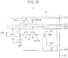
- Fig. 26 is a diagram illustrating a circuit configuration of a pixel constituting the solid-state imaging device according to the modified example 1-5 of the first embodiment.
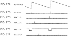
- Figs. 27A to 27F are diagram illustrating an operation of the solid-state imaging device according to the modified example 1-5 of the first embodiment.
- Figs. 27A to 27F show timing charts.
- Figs. 27A to 27F show a third readout signal (readout 3) transmitted to a control gate 15 via a readout line H43 in addition to the signals shown in Figs. 13A to 13E .
- control gate 15 may be further added to the configuration(refer to Fig. 12 ).
- control gate 15 may be formed so as to cover the part where the n-type impurity area 12 (accumulator 1) is formed in the surface of the silicon substrate 11.
- control gate 15 for example, an electric field is applied such that the signal charges (here, electrons) generated by the photoelectric conversion film 13 are moved to the n-type impurity area 12 through drift.
- an electric field may be applied to the control gate 15 such that the signal charges generated by the photoelectric conversion film 13 are temporarily accumulated and then moved to the n-type impurity area 12 (accumulator 1).
- control gate 15 is electrically connected to the readout line H43. Further, as shown in Figs. 27A to 27F , a potential at the control gate 15 may be controlled via the readout line H43.
- an electric field is applied to the control gate 15 for a long time such that the signal charges are moved from the photoelectric conversion film 13 to the n-type impurity area 12 (accumulator 1).
- the electric field is not applied to the control gate 15.
- the signal charges are moved from the n-type impurity area 12 (accumulator 1) to the n-type impurity region 411 (accumulator 2) by the gate MOS 41. Thereafter, the "PD reset" is made.
- the electric field is secondly applied to the control gate 15 for a long time such that the signal charges are moved from the photoelectric conversion film 13 to the n-type impurity area 12 (accumulator 1). During this interval, the amplified signal is read out in the same manner as in the first embodiment.
- control gate 15 is formed, this modified example is not limited to the above-described configuration.
- Fig. 28 is a diagram illustrating main portions of the solid-state imaging device according to the modified example 1-5 of the first embodiment.
- Fig. 28 shows a cross-section of the pixel P in the same manner as Fig. 25 .
- Fig. 29 is a diagram illustrating a circuit configuration of a pixel constituting the solid-state imaging device according to the modified example 1-5 of the first embodiment.
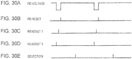
- Figs. 30A to 30E are diagrams illustrating an operation of the solid-state imaging device according to the modified example 1-5 of the first embodiment. Figs. 30A to 30E show timing charts.
- the respective portions may be driven without forming the gate MOS 42 and the n-type impurity region 411 (accumulator 2).
- the signal charges are instantly moved from the photoelectric conversion film 13 of all the pixels P to the n-type impurity area 12 (accumulator 1) (refer to the "readout 3"). Thereafter, in the same manner as the above-described case, the "readout 1" and the “selection” are performed, and an amplified signal is sequentially read out.
- Figs. 31A and 31B are diagrams illustrating a band structure of a solid-state imaging device according to a modified example 1-6 of the first embodiment.
- Figs. 31A and 31B in the same manner as Fig. 8 , show a band structure in the depth direction z of the photoelectric conversion film 13 and the silicon substrate 11.
- Fig. 31A shows a case where the photoelectric conversion film 13 with a band structure different from that in Fig. 8 is formed
- Fig. 31B shows a preferable case in that case.
- a lattice matching chalcopyrite material may not be constant in the band structure.
- the photoelectric conversion film 13 having the different band structure may be formed in some cases as can be seen from the comparison with Fig. 8 .
- an intermediate layer IT may be interposed between the silicon substrate 11 and the photoelectric conversion film 13.
- the electron affinity of the intermediate layer IT is formed to lie between the electron affinity of the silicon substrate 11 and the electron affinity of the photoelectric conversion film 13 in order to lower the potential barrier between the silicon substrate 11 and the photoelectric conversion film 13.
- the electron affinity of the intermediate layer IT has the following relation. (the electron affinity of the silicon substrate 11) ⁇ (the electron affinity of the intermediate layer IT) ⁇ (the electron affinity of the photoelectric conversion film 13)
- the electron affinity of the intermediate layer IT is exactly half the electron affinity of the silicon substrate 11 and the electron affinity of the photoelectric conversion film 13.
- the intermediate layer IT is preferably formed under the conditions of the following materials and film thickness.
- the intermediate layer IT may not be lattice-matched with the silicon substrate 11.
- the film thickness is 5 nm, the film thickness is smaller than the critical film thickness defined by the equation (1) by " Matthews and Blakeslee” (J. W. Mathews and A. E. Blakeslee, J. Cryst. Growth 27(1974) 118-125 ) and the equation (2) by "People and Bean” ( R. People and J. C. Bean, Appl. Phys. Lett. 47(1985) 322-324 ).
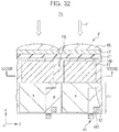
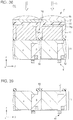
- Fig. 32 is a diagram illustrating main portions of a solid-state imaging device according to a second embodiment.
- Fig. 32 shows a cross-section of the pixel P in the same manner as Fig. 3 .
- a pixel dividing portion PB is provided. Further, instead of the transparent electrode 14, a p+ layer 14p is provided. Except for this, this embodiment is the same as the first embodiment. Therefore, the description of the overlapping parts will be omitted.
- the pixel dividing portion PB is interposed between the pixels P shown in Fig. 2 , and is provided to divide the pixels from each other.
- the pixel dividing portion PB is provided to extend in the horizontal direction x and the vertical direction y so as to be interposed between the pixels on the imaging surface (xy plane).
- the pixel dividing portion PB is provided on the lateral surface of the photoelectric conversion film 13 which is provided for each P on the one surface of the silicon substrate 11.
- the pixel dividing portion PB is made of semiconductors including p-type impurities.
- the pixel dividing portion PB is made of a chalcopyrite based compound semiconductor including p-type impurities with high concentration.
- the pixel dividing portion PB is formed to block the incident light H from entering the n-type impurity areas 12, 411 and 421 which function as an accumulator in the same manner as the photoelectric conversion film 13.
- the p+ layer 14p is made of a semiconductor including a p-type impurity on the upper surface of the photoelectric conversion film 13.
- the p+ layer 14p is formed with a high concentration of the impurity such that holes generated in the photoelectric conversion film 13 enter the p+ layer 14p and are moved in the transverse direction.
- the p+ layer 14p is made of a compound semiconductor with the chalcopyrite structure in the same manner as the photoelectric conversion film 13 and the pixel dividing portion PB.
- Fig. 33 is a diagram illustrating a band structure of the solid-state imaging device according to the second embodiment.
- Fig. 33 shows a band structure for the part XXXIII-XXXIII marked with the chain line in Fig. 32 .
- Fig. 33 shows a band structure for the parts where the photoelectric conversion film 13 and the pixel dividing portion PB are formed in the direction x along the surface of the silicon substrate 11.
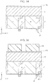
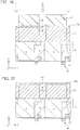
- Figs. 34 to 37 are diagrams illustrating the manufacturing method of the solid-state imaging device according to the second embodiment.
- Figs. 34 to 37 show the cross-sections in the same manner as Fig. 3 , and the solid-state imaging device 1 shown in Fig. 32 and the like is manufactured through the respective steps shown in Figs. 34 to 37 .
- the photoelectric conversion film 13 and the p+ layer 14p are formed as shown in Fig. 34 .
- the respective portions such as the gate MOS 41 are formed on the surface (front surface) of the silicon substrate 11 before the photoelectric conversion film 13 and the p+ layer 14p are formed in the same manner as the first embodiment. Further, the wire layer (not shown) is formed on the surface (front surface) of the silicon substrate 11 so as to cover the respective portions such as the gate MOS 41.
- the photoelectric conversion film 13 and the p+ layer 14p are sequentially formed on the opposite surface (rear surface) to the surface on which the respective portions such as the gate MOS 41 are formed in the silicon substrate 11.
- the photoelectric conversion film 13 is made of the compound semiconductor with the chalcopyrite structure in the same manner as the first embodiment. In this embodiment, the photoelectric conversion film 13 is formed to cover a part in which the pixel dividing portion PB is formed on the upper surface of the silicon substrate 11.
- the p+ layer 14p is formed to cover the upper surface of the photoelectric conversion film 13.
- the p+ layer 14p is also made of the compound semiconductor with the chalcopyrite structure.
- the p+ layer 14p is formed through the crystal growth of the compound semiconductor with the chalcopyrite structure under the condition of including a lot of an impurity such as Ga, In, As, or P, by the MOCVD method, the MBE method, or the like.
- the p+ layer 14p is formed with high concentration such that holes enter the p+ layer 14p and are moved in the transverse direction.
- the p+ layer 14p is formed to have the impurity concentration of 10 17 to 10 19 cm -3 .
- the p+ layer 14p is formed to have the film thickness of 10 to 100 nm.
- a resist pattern PR is formed.
- the resist pattern PR is formed on the p+ layer 14p.
- the resist pattern PR has apertures in order to expose a part of the upper surface of the p+ layer 14p under which the pixel dividing portion PB will be formed and to cover parts other than the exposed part.
- a photoresist film (not shown) is formed on the p+ layer 14p through application, and the resist pattern PR is formed by patterning the photoresist film by lithography.
- an impurity is ion-implanted into the photoelectric conversion film 13 by using the resist pattern PR as a mask.
- the impurity is ion-implanted into the part where the pixel dividing portion PB is formed in the photoelectric conversion film 13 from the aperture of the resist pattern PR.
- a p-type impurity such as Ga, In, As or P is ion-implanted into the part where the pixel dividing portion PB is formed in the photoelectric conversion film 13, and the p-type impurity is contained with a high concentration.
- the ion implantation is performed such that the concentration of the p-type impurity is 10 17 to 10 19 cm -3 in the part where the pixel dividing portion PB is formed.
- the resist pattern PR is removed from the upper surface of the p+ layer 14p.
- the pixel dividing portion PB is formed.
- the pixel dividing portion PB is formed by activation through annealing.
- the pixel dividing portion PB is formed through the annealing at a temperature of 400°C or more.
- the pixel dividing portion PB is formed by selectively doping the part forming the pixel dividing portion PB inside the photoelectric conversion film 13 which is formed to include the part forming the pixel dividing portion PB on the silicon substrate 11.
- the respective portions such as the color filters CF and the on-chip lenses ML are formed on the upper surface (rear surface) of the silicon substrate 11.
- the rear surface illumination-type CMOS image sensor is completed.
- the photoelectric conversion film 13 is provided at the side where the incident light H enters when seen from the respective portions such as the n-type impurity areas 12 and 411 in the silicon substrate 11, and thus blocks the incident light H from entering the n-type impurity areas 12 and 411 (refer to Fig. 32 ). For this reason, in this embodiment and in the same manner as the first embodiment, it is possible to realize a small size, prevent the generation of noise, and improve the image quality of a captured image.
- the pixel dividing portion PB is formed to be interposed between the plural pixels P.
- the pixel dividing portion PB is made of the compound semiconductor of which the doping concentration is controlled, so as to form potential barriers between the photoelectric conversion films 13 which are formed corresponding to the plural pixels P.
- the electrons generated through the photoelectric conversion are freely moved between the pixels. Assuming that the electrons are moved equally in all directions, about 30% of the electrons in a pixel of 1.5 ⁇ m are moved to neighboring pixels. The movement almost disappears due to the pixel dividing portion PB formed between the pixels P.
- the p+ layer 14p which is a diffusion layer of the impurity with high concentration, is formed on the surface of the photoelectric conversion film 13 at the side which the incident light enters. Therefore, it is possible to suppress the generation of a dark current.
- the p+ layer 14p is formed to be connected to each other among the plural pixels P. For this reason, holes enters the p+ layer 14p from the photoelectric conversion film 13 and then are moved to the pixels P in the transverse direction, and electrons generated in the photoelectric conversion film 13 are moved to the silicon substrate 11 side. Thereby, the transparent electrode may not be formed on the upper surface of the photoelectric conversion film 13.
- Fig. 38 is a diagram illustrating the main portions of a solid-state imaging device according to a third embodiment.
- Fig. 38 shows a cross-section of the pixel P in the same manner as Fig. 32 .
- an insulating film 80 is provided. Except for this, this embodiment is the same as the second embodiment. Therefore, the description of the overlapping parts will be omitted.
- the insulating film 80 is provided on one surface of the silicon substrate 11.
- the insulating film 80 is provided at the part forming the pixel dividing portion PB on the surface (rear surface) side opposite to the surface (front surface) on which the respective portions such as the gate MOS 41 and the like are provided.
- a silicon oxide film is provided as the insulating film 80.
- the insulating film 80 may be made of a material such as silicon nitride.
- the insulating film 80 is provided on surfaces of parts other than the parts forming the photoelectric conversion film 13 such that the photoelectric conversion film 13 is selectively crystal-grown on the surface (rear surface) of the silicon substrate 11.
- the pixel dividing portion PB is provided on the silicon substrate 11 with the insulating film 80 interposed therebetween.
- Figs. 39 to 41 are diagrams illustrating a manufacturing method of the solid-state imaging device according to the third embodiment.
- Figs. 39 to 41 show the cross-sections in the same manner as Fig. 38 , and the solid-state imaging device shown in Fig. 38 is manufactured through the respective steps shown in Figs. 39 to 41 .
- the insulating film 80 is formed as shown in Fig. 39 .
- the respective portions such as the gate MOS 41 are formed on the surface of the silicon substrate 11 before the insulating film 80 is formed in the same manner as the first embodiment. Further, the wire layer (not shown) is formed on the surface (front surface) of the silicon substrate 11 so as to cover the respective portions such as the gate MOS 41.
- the insulating film 80 is formed in the parts in which the pixel dividing portion PB is formed on the opposite surface (rear surface) to the surface on which the respective portions such as the gate MOS 41 are formed in the silicon substrate 11. In other words, the insulating film 80 is formed to partition the plural pixels P.
- a silicon oxide film (not shown) is formed to cover the rear surface (upper surface) of the silicon substrate 11. Thereafter, the silicon oxide film is patterned to form the insulating film 80 by the photolithography method.
- the insulating film 80 is formed to have the film thickness of 50 to 100 nm.
- the photoelectric conversion film 13 is formed.
- the photoelectric conversion film 13 is sequentially formed on the opposite surface (rear surface) to the surface on which the respective portions such as the gate MOS 41 are formed in the silicon substrate 11.
- the photoelectric conversion film 13 is made of the compound semiconductor with the chalcopyrite structure.
- the photoelectric conversion film 13 is formed on the silicon substrate 11 through the epitaxial growth of the compound semiconductor by the MOCVD method, the MBE method, or the like.
- the compound semiconductor is epitaxially grown to selectively cover the parts forming the photoelectric conversion films on the upper surface of the silicon substrate 11, and the photoelectric conversion films 13 are formed.
- the insulating film 80 is formed to partition the plural pixels P on the silicon substrate 11. For this reason, on the surface of the silicon substrate 11, the photoelectric conversion films 13 are formed on the exposed parts other than the parts forming the insulating films 80. Here, the photoelectric conversion film 13 is formed to be thicker than the insulating film 80. Thereby, trenches TR are provided between the photoelectric conversion films 13 provided to correspond to the respective pixels P.
- the pixel dividing portion PB and the p+ layer 14p are formed as shown in Fig. 41 .
- the pixel dividing portion PB and the p+ layer 14p are formed on the opposite surface (rear surface) to the surface on which the respective portions such as the gate MOS 41 are formed in the silicon substrate 11.
- the pixel dividing portion PB and the p+ layer 14p are formed such that the pixel dividing portion PB covers the insulating film 80 and the p+ layer 14p covers the photoelectric conversion film 13.
- each of the pixel dividing portion PB and the p+ layer 14p is made of a compound semiconductor with the chalcopyrite structure.
- the compound semiconductor is laterally grown under the condition of including a lot of an impurity such as Ga, In, As, or P.
- an impurity such as Ga, In, As, or P.
- the pixel dividing portion PB and the p+ layer 14p are formed to have the impurity concentration of 10 17 to 10 19 cm -3 .
- the pixel dividing portion PB is formed through the crystal growth of the compound semiconductor so as to cover the part forming the pixel dividing portion PB.
- the p+ layer 14p is formed through the crystal growth of the compound semiconductor so as to cover the upper surface of the photoelectric conversion film 13.
- the respective portions such as the color filters CF and the on-chip lenses ML are formed on the upper surface (rear surface) of the silicon substrate 11.
- the rear surface illumination-type CMOS image sensor is completed.
- the photoelectric conversion film 13 is provided at the side where the incident light H enters when seen from the respective portions such as the n-type impurity areas 12 and 411 in the silicon substrate 11, and thus blocks the incident light H from entering the n-type impurity areas 12 and 411 (refer to Fig. 38 ).
- the photoelectric conversion film 13 it is possible to realize a small size, prevent the generation of noise, and improve the image quality of a captured image.
- the pixel dividing portion PB is formed to be interposed between the pixels P in the same manner as the second embodiment.
- the pixel dividing portion PB is provide so as to form potential barriers between the photoelectric conversion films 13 which are formed corresponding to the plural pixels P. Thereby, in this embodiment, it is possible to prevent a color mixture using the pixel dividing portion PB.
- This embodiment is appropriate in terms of manufacturing costs since the number of process steps such as the ion implantation and the annealing is reduced as compared with the above-described embodiments. Further, since the ion implantation or the annealing is not performed, there is no damage caused by the processes (for example, damage during the ion implantation or an adverse effect on the wire layer during the annealing).
- Fig. 42 is a diagram illustrating main portions of a solid-state imaging device according to a fourth embodiment.
- Fig. 42 shows a cross-section of the pixel P in the same manner as Fig. 38 .
- a pixel dividing portion PBc is provided unlike the third embodiment. Except for this, this embodiment is the same as the third embodiment. Therefore, the description of the overlapping parts will be omitted.
- the pixel dividing portion PBc as shown in Fig. 42 , is provided to cover the insulating film 80 between the plural photoelectric conversion films 13 formed corresponding to the pixels P.
- the pixel dividing portion PBc is made of a semiconductor which does not include p-type impurities unlike the second embodiment.
- the pixel dividing portion PBc is made of a chalcopyrite based compound semiconductor having a wide band gap.
- Figs. 43 and 44 are diagrams illustrating a manufacturing method of the solid-state imaging device according to the fourth embodiment.
- Figs. 43 and 44 show the cross-sections in the same manner as Fig. 42 , and the solid-state imaging device shown in Fig. 42 is manufactured through the respective steps shown in Figs. 43 and 44 .
- the pixel dividing portion PBc is formed.
- the insulating film 80 and the photoelectric conversion film 13 are formed in the same manner as the second embodiment before the pixel dividing portion PBc is formed (refer to Figs. 39 and 40 ).
- the pixel dividing portion PBc is formed to cover the insulating film 80 between the plural photoelectric conversion films 13 formed corresponding to the pixels P.
- the pixel dividing portion PBc is formed, for example, using a chalcopyrite based compound semiconductor having a wide band gap.
- the compound semiconductor is laterally grown under a condition of not including p-type impurities. Thereby, the compound semiconductor is implanted into the trench TR between the photoelectric conversion films 13.
- the pixel dividing portion PBc is formed such that a composition ratio of copper-aluminum-gallium-indium-sulfur-selenium is 1.0:0.36:0.64:0:1.28:0.72, or 1.0:0.24:0.23:0.53:2.0:0. That is to say, the pixel dividing portion PBc is formed to give CuAl 0.36 Ga 0.64 S 1.28 Se 0.72 or CuAl 0.24 Ga 0.23 In 0.53 S 2 .
- the p+ layer 14p is formed.
- the p+ layer 14p is formed to cover the photoelectric conversion films 13 and the pixel dividing portions PBc on the rear surface (upper surface) side of the silicon substrate 11.
- the p+ layer 14p is made of a compound semiconductor with the chalcopyrite structure in the same manner as the second embodiment.
- the compound semiconductor is crystal-grown under the condition of including a lot of an impurity such as Ga, In, As, or P, thereby forming the p+ layer 14p.
- the respective portions such as the color filters CF and the on-chip lenses ML are formed on the upper surface (rear surface) of the silicon substrate 11.
- the rear surface illumination-type CMOS image sensor is completed.
- the photoelectric conversion film 13 is provided at the side where the incident light H enters when seen from the respective portions such as the n-type impurity areas 12 and 411 in the silicon substrate 11, and thus blocks the incident light H from entering the n-type impurity areas 12 and 411 (refer to Fig. 42 ).
- the photoelectric conversion film 13 it is possible to realize a small size, prevent the generation of noise, and improve the image quality of a captured image.
- the pixel dividing portion PBc is made of the compound semiconductor of which the composition is controlled, so as to form potential barriers between the photoelectric conversion films 13 which are formed corresponding to the plural pixels P. Thereby, in this embodiment, it is possible to prevent a color mixture using the pixel dividing portion PBc.
- the crystallinity of the pixel dividing portion PBc is good as compared with the cases of other embodiments.
- this embodiment is appropriate in terms of manufacturing costs since the number of process steps such as the ion implantation and the annealing is reduced as compared with other embodiments.
- Fig. 45 is a diagram illustrating main portions of a solid-state imaging device according to a fifth embodiment.
- Fig. 45 shows a cross-section of the pixel P in the same manner as Fig. 3 .
- this embodiment is different from the modified example 1-5 of the first embodiment in that electrodes 511 and 531, and a contact 521 are further provided. Except for this, this embodiment is the same as the modified example 1-5 of the first embodiment. Therefore, the description of the overlapping parts will be omitted.
- a set of the electrodes 511 and 531 and the contact 521 are formed corresponding to each pixel P as shown in Fig. 45 .
- the electrodes 511 and 531 and the contact 521 are formed on the upper surface of the n-type impurity area 12 formed for each pixel P.
- An insulating layer 54 is provided around the pixels P to insulate each other of the pixels P.
- the electrodes 511 and 531 and the contact 521 make an electric connection between the photoelectric conversion film 13 and the n-type impurity area 12, and thus the signal charges generated in the photoelectric conversion film 13 are moved to the n-type impurity area 12 via the electrodes 511 and 531 and the contact 521.
- the electrodes 511 and 531 are formed using metal materials, and block light from above.
- the photoelectric conversion film 13 is provided at the side where the incident light H enters when seen from the respective portions such as the n-type impurity areas 12 and 411 in the silicon substrate 11, and thus blocks the incident light H from entering the n-type impurity areas 12 and 411 (refer to Fig. 45 ).
- the electrodes 511 and 531 are formed as lower electrodes in the lower side of the photoelectric conversion film 13, and the electrodes 511 and 531 block the incident light H from entering the n-type impurity areas 12 and 411 and the like (refer to Fig. 45 ). In other words, in this embodiment, due to the combination of the photoelectric conversion film 13 and the lower electrode 531, the incident light H is blocked.
- the photoelectric conversion film 13 has a light blocking function
- this embodiment is not limited thereto.
- the entire photoelectric conversion unit including the photoelectric conversion film 13 and the electrodes 511 and 531 functioning as the lower electrodes may realize the light blocking function.
- Fig. 46 is a diagram illustrating main portions of a solid-state imaging device according to a sixth embodiment.
- Fig. 46 shows a cross-section of the pixel P in the same manner as Fig. 45 .
- a position of the gate MOS 41 is different. Also, the n-type impurity area 12 is different. Except for this and parts related thereto, this embodiment is the same as the fifth embodiment. Therefore, the description of the overlapping parts will be omitted.
- the electrodes 511 and 531 and the contact 521 are provided on the upper surface of the silicon substrate 11 in the same manner as the fifth embodiment.
- the gate MOS 41 is also provided on the upper surface of the silicon substrate 11.
- the gate MOS 42 and the readout circuit 51 are provided separately in addition to the gate MOS 41. Wires connected to the respective portions such as the gate MOS 41 and the like are provided on one surface of the silicon substrate 11.
- the n-type impurity area 12 is provided inside the silicon substrate 11 in the same manner as the fifth embodiment. However, unlike the fifth embodiment, the n-type impurity area 12 is provided on the upper surface side of the silicon substrate 11 and is not provided around the lower surface.
- the wire layer (not shown) is not provided on the upper surface of the silicon substrate 11 unlike the fifth embodiment.
- the photoelectric conversion film 13 senses the incident light H coming from the upper surface (front surface) on which the respective portions such as the photoelectric conversion film 13 are provided on the silicon substrate 11.
- the solid-state imaging device in this embodiment is a "front surface illumination-type CMOS image sensor.”
- the photoelectric conversion film 13 is provided at the side where the incident light H enters when seen from the respective portions such as the n-type impurity areas 12 and 411 in the silicon substrate 11, and thus blocks the incident light H from entering the n-type impurity areas 12 and 411 (refer to Fig. 46 ).
- the electrodes 511 and 531 are formed as lower electrodes in the lower side of the photoelectric conversion film 13, and the electrodes 511 and 531 block the incident light H from entering the n-type impurity areas 12 and 411 and the like (refer to Fig. 46 ). In other words, in this embodiment, due to the combination of the photoelectric conversion film 13 and the lower electrode 531, the incident light H is blocked.
- the photoelectric conversion film 13 has a light blocking function
- this embodiment is not limited thereto.
- the entire photoelectric conversion unit including the photoelectric conversion film 13 and the electrodes 511 and 531 functioning as the lower electrodes may realize the light blocking function.
- the silicon substrate of which a main surface is the (100) plane is used the above-described compound semiconductor is epitaxially grown in the main surface, thereby forming the photoelectric conversion film.
- the case of using the ⁇ 100 ⁇ substrate has been described.
- the present invention is not limited thereto.
- a tilted substrate may be used as the silicon substrate. It is possible to suppress the generation of the antiphase domain through the epitaxial growth on a tilted substrate (refer to Mitsuhisa Kawabe, Hidetoshi Takasugi, Toshio Ueda, and Akira Yokoyama, and Yoshio Bando: Initial Growth Process of GaAs on Si; Division of Crystals Science and Technology, 4th Crystal Engineering Symposium Text (1987. 7. 17) pp. 1-8 )
- Figs. 47 to 49 are diagrams illustrating atomic arrangements when a photoelectric conversion film 13k is formed on a silicon substrate 11k which is a tilted substrate in the seventh embodiment.
- Figs. 47 to 49 are respectively cross-sectional views of a crystal when seen from the ⁇ 0 - 1 1> direction.
- a Group I atom is a copper (Cu) atom
- a Group III atom is a gallium (Ga) atom or an indium (In) atom
- a Group VI atom is a sulfur (S) atom, a selenium (Se) atom, or the like.
- the atomic positions labelled "Group I atom or Group III atom" shown with the white squares indicate that Group I atoms and Group III atoms are alternately arranged in the direction perpendicular to the paper. Also, in Fig.
- Fig. 47 shows that the growth starts from the Group VI atom on the silicon substrate 11k.
- Fig. 48 shows that the growth starts from the Group I atom or the Group III atom.
- Figs. 47 and 48 show a case where the antiphase domain between the cation (positive ionic atom) the Group I atom or the Group III atom and the anion (negative ionic atom) of the Group VI atom is annihilated.
- Fig. 49 shows that the antiphase domain between the Group I atom and the Group III atom is annihilated.
- the tilted substrate in which, for example, the main surface is tilted with a predetermined tilt angle (off angle, off axis angle or tilt angle) ⁇ 1 in the ⁇ 011> direction from the (100) plane is used as the silicon substrate 11k.
- the tilted substrate in which a ⁇ 100 ⁇ substrate is off in the ⁇ 011> direction is used as the silicon substrate 11k.
- a tilted substrate of which the tilt angle (off angle) ⁇ 1 is about 6° is used.
- the cation (positive ionic atom) of the Group I or the Group III and the anion (negative ionic atom) of the Group VI are regularly arranged to form the photoelectric conversion film 13k.
- the cation and the anion are grown in the antiphase locally as in the area B (area marked with the chain lines), thereby generating the antiphase domain.
- the crystal is grown on the main surface of the tilted substrate, and the area B in which the antiphase domain is generated is closed in the triangular shape.
- Fig. 50 is an enlarged perspective view of the area B in which the antiphase domain is generated when the photoelectric conversion film 13k is formed on the silicon substrate 11k in the seventh embodiment.
- the antiphase domain with the triangular cross-section is formed to consecutively extend in the depth direction ( ⁇ 0 -1 1> direction).
- the antiphase domain is formed in such a shape that a triangular prism reclines in the side.
- the epitaxial growth is performed to generate only the area A in which the antiphase domain is not generated, in the upper side of the area B.
- the height of the triangle of the area B becomes about 5 nm.
- the thickness necessary for the photoelectric conversion film is equal to or more than about 120 nm at the light absorption coefficient of 10 5 cm -1 (at this time, 70% or more of light is absorbed).
- the tilt angle ⁇ 1 is 2°C, the height of the triangle of the area B is settled to a degree of about 15 nm.
- the upper limit value is an angle until a stepwise substrate structure can be maintained. Specifically, ⁇ 1 allows 90° to the maximum.
- the photoelectric conversion film 13k is formed by epitaxially growing the compound semiconductor on the silicon substrate 11k which is a tilted substrate. Thereby, as described above, it is possible to suppress the antiphase domain from being generated.
- Fig. 51 is a diagram illustrating main portions of a solid-state imaging device according to an eighth embodiment.
- Fig. 51 schematically shows a cross-section of the pixel P.
- a red photoelectric conversion film 13R, a green photoelectric conversion film 13G, and a blue photoelectric conversion film 13B are provided as the photoelectric conversion film 13.
- the red photoelectric conversion film 13R, the green photoelectric conversion film 13G, and the blue photoelectric conversion film 13B are respectively provided with upper electrodes 14R, 14G and 14B and lower electrodes 53R, 53G and 53B.
- the accumulator 12R, 12G and 12B which are the n-type impurity area 12 are respectively provided in the red photoelectric conversion film 13R, the green photoelectric conversion film 13G, and the blue photoelectric conversion film 13B.
- the color filter CF is not provided. Except for this and parts related thereto, this embodiment is the same as the sixth embodiment. Therefore, the description of the overlapping parts will be omitted.
- the photoelectric conversion film 13 includes the red photoelectric conversion film 13R, the green photoelectric conversion film 13G, and the blue photoelectric conversion film 13B, which are sequentially laminated on the front surface of the silicon substrate 11.
- the red photoelectric conversion film 13R of the photoelectric conversion film 13 is provided in the upper side of the surface of the silicon substrate 11 as shown in Fig. 51 .
- the red photoelectric conversion film 13R selectively disperses a red light beam of the incident light beams H coming from above and photoelectric-converts the red light beam.
- the red photoelectric conversion film 13R is provided to sense with high sensitivity a light beam in a red wavelength band of light beams passing through the respective portions and generate charges through the photoelectric conversion.
- the green photoelectric conversion film 13G of the photoelectric conversion film 13 is provided on the upper side of the surface of the silicon substrate 11 with the red photoelectric conversion film 13R interposed between it and the substrate as shown in Fig. 51 .
- the green photoelectric conversion film 13G selectively disperses a green light beam of the incident light beams H coming from above and photoelectric-converts the green light beam.
- the green photoelectric conversion film 13G is provided to sense with high sensitivity a light beam in a green wavelength band of light beams passing through the respective portions and generate charges through the photoelectric conversion.
- the blue photoelectric conversion film 13B of the photoelectric conversion film 13 is provided on the upper side of the surface of the silicon substrate 11 with the red photoelectric conversion film 13R and the green photoelectric conversion film 13G interposed between it and the substrate as shown in Fig. 51 .
- the blue photoelectric conversion film 13B selectively disperses a blue light beam of the incident light beams H coming from above and photoelectric-converts the blue light beam.
- the blue photoelectric conversion film 13B is provided to sense with high sensitivity a light beam in a blue wavelength band of light beams passing through the respective portions and generate charges through the photoelectric conversion.
- the red photoelectric conversion film 13R, the green photoelectric conversion film 13G, and the blue photoelectric conversion film 13B are respectively provided with the upper electrodes 14R, 14G and 14B and the lower electrodes 53R, 53G and 53B between them and the silicon substrate 11 in the depth direction z of the silicon substrate 11.
- the upper electrodes 14R, 14G and 14B are respectively provided on the upper surfaces of the red photoelectric conversion film 13R, the green photoelectric conversion film 13G, and the blue photoelectric conversion film 13B, and are electrically connected to the ground.
- the lower electrodes 53R, 53G and 53B are respectively on the lower surfaces of the red photoelectric conversion film 13R, the green photoelectric conversion film 13G, and the blue photoelectric conversion film 13B, and are electrically connected to the n-type impurity area 12 which is provided as accumulators 12R, 12G and 12B in the silicon substrate 11.
- insulating films are interposed between the combinations of the respective red photoelectric conversion film 13R, the green photoelectric conversion film 13G, and the blue photoelectric conversion film 13B, and the upper electrodes 14R, 14G and 14B and the lower electrodes 53R, 53G and 53B.
- the red photoelectric conversion film 13R, the green photoelectric conversion film 13G, and the blue photoelectric conversion film 13B are respectively formed using, for example, organic materials.
- Figs. 52A to 52C are diagrams illustrating examples used as materials when the red photoelectric conversion film 13R, the green photoelectric conversion film 13G, and the blue photoelectric conversion film 13B are formed in the eighth embodiment.
- Fig. 52A shows an example of a material used when the red photoelectric conversion film 13R is formed.
- Fig. 52B shows an example of a material used when the green photoelectric conversion film 13G is formed.
- Fig. 52C shows an example of a material used when the blue photoelectric conversion film 13B is formed.
- the red photoelectric conversion film 13R is formed using, for example, ZnPc.
- the green photoelectric conversion film 13G is formed using, for example, quinacridone.
- the blue photoelectric conversion film 13B is formed using, for example, BCzVBi.
- Each of the red photoelectric conversion film 13R, the green photoelectric conversion film 13G, and the blue photoelectric conversion film 13B is formed to have the film thickness of 100 nm or more.
- Each of the upper electrodes 14R, 14G and 14B and the lower electrodes 53R, 53G and 53B is a transparent electrode, and allows light to pass therethrough.
- each of them is formed by forming a film of metal oxide such as indium tin oxide (ITO) using a film forming method such as a sputtering method.
- ITO indium tin oxide
- the solid-state imaging device in this embodiment is a "photoelectric conversion film laminated type" image sensor, and disperses the incident light H into the respective colors of red, green and blue in the depth direction z for the photoelectric conversion.
- the incident light H is blocked from entering the silicon substrate 11.
- Figs. 53A and 53B are diagrams illustrating the characteristics of the red photoelectric conversion film 13R, the green photoelectric conversion film 13G, and the blue photoelectric conversion film 13B in the eighth embodiment.
- Fig. 53A shows a relationship between the wavelength of the incident light and the photoelectric conversion efficiency regarding each of the red photoelectric conversion film 13R, the green photoelectric conversion film 13G, and the blue photoelectric conversion film 13B.
- Fig. 53B shows a relationship between the wavelength of the incident light and the light transmittance regarding each of the red photoelectric conversion film 13R, the green photoelectric conversion film 13G, and the blue photoelectric conversion film 13B.
- the chain line denotes the case of the red photoelectric conversion film 13R
- the solid line denotes the case of the green photoelectric conversion film 13G
- the broken line denotes the case of the blue photoelectric conversion film 13B.
- the photoelectric conversion is performed with the high photoelectric conversion efficiency throughout the visible region.
- the visible light does not enter the accumulators 12R, 12G and 12B provided in the lower side of the photoelectric conversion film 13 but is blocked by the photoelectric conversion film 13.
- light in the infrared region is cut by forming an infrared cutoff filter in the upper side of the photoelectric conversion film 13.
- light in the ultraviolet region is cut by forming an ultraviolet cutoff filter in the upper side of the photoelectric conversion film 13.
- the plural photoelectric conversion films 13R, 13G and 13B having different absorption spectra are provided, and the plural photoelectric conversion films 13R, 13G and 13B are laminated. Due to the combination of the plural laminated photoelectric conversion films 13R, 13G and 13B, the incident light H is blocked from entering the silicon substrate 11.
- the plural photoelectric conversion films 13R, 13G and 13B block the incident light H from entering the n-type impurity area 12 and the like, in the same manner as other embodiments, it is possible to realize a small size, prevent the generation of noise, and improve the image quality of a captured image.
- Fig. 54 is a diagram illustrating main portions of a solid-state imaging device according to a ninth embodiment.
- Fig. 54 shows a cross-section of the pixel P in the same manner as Fig. 45 .
- this embodiment is different from the fifth embodiment in a configuration of the photoelectric conversion film 13. Except for this, this embodiment is the same as the fifth embodiment.
- the photoelectric conversion film 13 has the same configuration as that in the eighth embodiment. Therefore, the description of the overlapping parts will be omitted.
- the photoelectric conversion film 13 includes the red photoelectric conversion film 13R, the green photoelectric conversion film 13G, and the blue photoelectric conversion film 13B, which are sequentially laminated on the front surface of the silicon substrate 11.
- the red photoelectric conversion film 13R is provided in the upper side of the surface of the silicon substrate 11, and selectively disperses a red light beam of the incident light beams H coming from above and photoelectric-converts the red light beam.
- the green photoelectric conversion film 13G is provided on the upper side of the surface of the silicon substrate 11 with the red photoelectric conversion film 13R interposed between it and the substrate, and selectively disperses a green light beam of the incident light beams H coming from above and photoelectric-converts the green light beam.
- the blue photoelectric conversion film 13B is provided on the upper side of the surface of the silicon substrate 11 with the red photoelectric conversion film 13R and the green photoelectric conversion film 13G interposed between it and the substrate, and selectively disperses a blue light beam of the incident light beams H coming from above and photoelectric-converts the blue light beam.
- the color filters CF are provided over the photoelectric conversion film 13. For this reason, the light passing through the color filters CF is sensed by the red photoelectric conversion film 13R, the green photoelectric conversion film 13G, and the blue photoelectric conversion film 13B.
- a red light beam passing through a red filter layer (not shown) is sensed by the red photoelectric conversion film 13R and undergoes the photoelectric conversion.
- a green light beam passing through a green filter layer (not shown) is sensed by the green photoelectric conversion film 13G and undergoes the photoelectric conversion.
- a blue light beam passing through a blue filter layer is sensed by the blue photoelectric conversion film 13B and undergoes the photoelectric conversion.
- the red photoelectric conversion film 13R, the green photoelectric conversion film 13G, and the blue photoelectric conversion film 13B are respectively are formed using, for example, organic materials in the same manner the eighth embodiment.
- materials such as a chalcopyrite based material may be used.
- the solid-state imaging device in this embodiment is a "photoelectric conversion film laminated type" image sensor, and disperses the incident light H into the respective colors of red, green and blue in the depth direction z for the photoelectric conversion.
- the incident light H is blocked from entering the silicon substrate 11.
- Fig. 55 is a diagram illustrating the characteristics of the red photoelectric conversion film 13R, the green photoelectric conversion film 13G, and the blue photoelectric conversion film 13B in the ninth embodiment.
- Fig. 55 shows a relationship between the wavelength of the incident light and the light absorption coefficient regarding each of the red photoelectric conversion film 13R, the green photoelectric conversion film 13G, and the blue photoelectric conversion film 13B.
- the chain line denotes the case of the red photoelectric conversion film 13R
- the solid line denotes the case of the green photoelectric conversion film 13G
- the broken line denotes the case of the blue photoelectric conversion film 13B.
- the red photoelectric conversion film 13R, the green photoelectric conversion film 13G, and the blue photoelectric conversion film 13B are combined, the light is absorbed throughout the visible region. Therefore, the visible light does not enter the n-type impurity area 12 provided in the lower side of the photoelectric conversion film 13 but is blocked by the photoelectric conversion film 13.
- the light passing through the color filters CF is absorbed by the red photoelectric conversion film 13R, the green photoelectric conversion film 13G, and the blue photoelectric conversion film 13B, the light is efficiently blocked.
- the plural photoelectric conversion films 13R, 13G and 13B having different absorption spectra are provided, and the plural photoelectric conversion films 13R, 13G and 13B are laminated. Due to the combination of the plural laminated photoelectric conversion films 13R, 13G and 13B, the incident light H is blocked from entering the silicon substrate 11.
- the plural photoelectric conversion films 13R, 13G and 13B block the incident light H from entering the n-type impurity area 12 and the like, in the same manner as other embodiments, it is possible to realize a small size, prevent the generation of noise, and improve the image quality of a captured image.
- Fig. 56 is a diagram illustrating main portions of a solid-state imaging device according to a tenth embodiment.
- Fig. 56 shows a cross-section of the pixel P in the same manner as Fig. 46 .
- this embodiment is different from the sixth embodiment in a configuration of the photoelectric conversion film 13. Except for this, this embodiment is the same as the sixth embodiment.
- the photoelectric conversion film 13 has the same configuration as that in the ninth embodiment. Therefore, the description of the overlapping parts will be omitted.
- the photoelectric conversion film 13 senses the incident light H coming from the upper surface (front surface) on which the respective portions such as the gate MOS 41 are provided on the silicon substrate 11.
- the solid-state imaging device in this embodiment is a "front surface illumination-type CMOS image sensor.”
- the photoelectric conversion film 13 includes the red photoelectric conversion film 13R, the green photoelectric conversion film 13G, and the blue photoelectric conversion film 13B, which are sequentially laminated on the front surface of the silicon substrate 11 (refer to Fig. 54 ).
- the solid-state imaging device in this embodiment is a "photoelectric conversion film laminated type" image sensor, and disperses the incident light H into the respective colors of red, green and blue in the depth direction z for the photoelectric conversion.
- the incident light H is blocked from entering the silicon substrate 11.
- the red photoelectric conversion film 13R, the green photoelectric conversion film 13G, and the blue photoelectric conversion film 13B are combined, the light is absorbed throughout the visible region. Therefore, the visible light does not enter the n-type impurity area 12 provided in the lower side of the photoelectric conversion film 13 but is blocked by the photoelectric conversion film 13.
- the plural photoelectric conversion films 13R, 13G and 13B having different absorption spectra are provided, and the plural photoelectric conversion films 13R, 13G and 13B are laminated. Due to the combination of the plural laminated photoelectric conversion films 13R, 13G and 13B, the incident light H is blocked from entering the silicon substrate 11.
- the plural photoelectric conversion films 13R, 13G and 13B block the incident light H from entering the n-type impurity area 12 and the like, in the same manner as other embodiments, it is possible to realize a small size, prevent the generation of noise, and improve the image quality of a captured image.
- Fig. 57 is a diagram illustrating main portions of a solid-state imaging device according to an eleventh embodiment.
- Fig. 57 shows a cross-section of the pixel P in the same manner as Fig. 45 .
- this embodiment is different from the fifth embodiment in a configuration of the photoelectric conversion film 13. Except for this, this embodiment is the same as the fifth embodiment. Therefore, the description of the overlapping parts will be omitted.
- the photoelectric conversion film 13 includes the red photoelectric conversion film 13R and the green photoelectric conversion film 13G, which are provided to be arranged along the front surface of the silicon substrate 11.
- the photoelectric conversion film 13 further includes the blue photoelectric conversion film 13B in addition to the red photoelectric conversion film 13R and the green photoelectric conversion film 13G, and the blue photoelectric conversion film 13B is arranged along with the red photoelectric conversion film 13R and the green photoelectric conversion film 13G.
- the photoelectric conversion film 13 blocks the incident light H due to the combination of the red photoelectric conversion film 13R, the green photoelectric conversion film 13G, and the blue photoelectric conversion film 13B, the red filter layer CFR, the green filter layer CFG, and the blue filter layer CFB.
- the red color filter layer CFR as the color filter CF is provided over the red photoelectric conversion film 13R, and a red light beam passing through the red color filter layer CFR enters the red photoelectric conversion film 13R.
- the green color filter layer CFG as the color filter CF is provided over the green photoelectric conversion film 13G, and a green light beam passing through the green color filter layer CFG enters the green photoelectric conversion film 13G.
- the blue color filter layer CFB as the color filter CF is provided over the blue photoelectric conversion film 13B, and a blue light beam passing through the blue color filter layer CFB enters the blue photoelectric conversion film 13B.
- the red photoelectric conversion film 13R, the green photoelectric conversion film 13G, and the blue photoelectric conversion film 13B are arranged in the Bayer arrangement in the same manner as the red filter layer CFR, the green filter layer CFG, and the blue filter layer CFB constituting the color filter CF.
- Fig. 58 is a diagram illustrating the characteristics of the green photoelectric conversion film 13G and the green filter layer CFG in the eleventh embodiment.
- Fig. 58 shows a relationship between the wavelength of the incident light and the light absorption coefficient regarding each of the green photoelectric conversion film 13G and the green filter layer CFG.
- the solid line denotes the case of the green photoelectric conversion film 13G
- the broken line denotes the case of the green filter layer CFG.
- the green photoelectric conversion film 13G has the high light absorption coefficient with respect to light in the wavelength region corresponding to the green.
- the green filter layer CFG has the high light absorption coefficient with respect to light in the visible region other than the wavelength region corresponding to the green.
- the green photoelectric conversion film 13G and the green filter layer CFG are combined, the light is absorbed throughout the visible region. Therefore, the visible light does not enter the n-type impurity area 12 provided in the lower side of the green photoelectric conversion film 13G but is blocked by the photoelectric conversion film 13.
- the red photoelectric conversion film 13R and the red filter layer CFR are combined as well, the light is absorbed throughout the visible region. Therefore, the visible light does not enter the n-type impurity area 12 provided in the lower side of the red photoelectric conversion film 13R but is blocked by the photoelectric conversion film 13.
- the blue photoelectric conversion film 13B and the blue filter layer CFB are combined as well, the light is absorbed throughout the visible region. Therefore, the visible light does not enter the n-type impurity area 12 provided in the lower side of the blue photoelectric conversion film 13B but is blocked by the photoelectric conversion film 13.
- the photoelectric conversion film 13 blocks the incident light H due to the combination of the red photoelectric conversion film 13R, the green photoelectric conversion film 13G, and the blue photoelectric conversion film 13B, the red filter layer CFR, the green filter layer CFG, and the blue filter layer CFG.
- the plural photoelectric conversion film 13 blocks the incident light H from entering the n-type impurity area 12 and the like, in the same manner as other embodiments, it is possible to realize a small size, prevent the generation of noise, and improve the image quality of a captured image.
- Fig. 59 is a diagram illustrating main portions of a solid-state imaging device according to a twelfth embodiment.
- Fig. 59 shows a cross-section of the pixel P in the same manner as Fig. 46 .
- this embodiment is different from the sixth embodiment in a configuration of the photoelectric conversion film 13. Except for this, this embodiment is the same as the sixth embodiment.
- the photoelectric conversion film 13 has the same configuration as that in the eleventh embodiment. Therefore, the description of the overlapping parts will be omitted.
- the photoelectric conversion film 13 senses the incident light H coming from the upper surface (front surface) on which the respective portions such as the gate MOS 41 are provided on the silicon substrate 11.
- the solid-state imaging device in this embodiment is a "front surface illumination-type CMOS image sensor.”
- the photoelectric conversion film 13 includes the red photoelectric conversion film 13R and the green photoelectric conversion film 13G, and the like, which are provided to be arranged along the front surface of the silicon substrate 11.
- the photoelectric conversion film 13 further includes the blue photoelectric conversion film 13B in addition to the red photoelectric conversion film 13R and the green photoelectric conversion film 13G, and the blue photoelectric conversion film 13B is arranged along with the red photoelectric conversion film 13R and the green photoelectric conversion film 13G.
- the photoelectric conversion film 13 blocks the incident light H due to the combination of the red photoelectric conversion film 13R, the green photoelectric conversion film 13G, and the blue photoelectric conversion film 13B, the red filter layer CFR, the green filter layer CFG, and the blue filter layer CFB.
- the red photoelectric conversion film 13R, the green photoelectric conversion film 13G, and the blue photoelectric conversion film 13B are arranged in the Bayer arrangement in the same manner as the red filter layer CFR, the green filter layer CFG, and the blue filter layer CFB constituting the color filter CF.
- the photoelectric conversion film 13 blocks the incident light H due to the combination of the red photoelectric conversion film 13R, the green photoelectric conversion film 13G, and the blue photoelectric conversion film 13B, the red filter layer CFR, the green filter layer CFG, and the blue filter layer CFB.
- the photoelectric conversion film 13 blocks the incident light H from entering the n-type impurity area 12 and the like, in the same manner as other embodiments, it is possible to realize a small size, prevent the generation of noise, and improve the image quality of a captured image.
- the present invention may be applied to other electronic devices including a solid-state imaging device such as a scanner or a copier.
- the present invention is not limited thereto. If necessary, the present invention may be applied to a CCD type image sensor in addition to the CMOS image sensor.
- a readout circuit may be singly provided in a plurality of photoelectric conversion units. That is to say, plural pixels may share transistors so as to reduce the number of the transistors. Thereby, finer pixels can be realized.
- a second conductivity type for example, an n-type impurity area is formed in a first conductivity type (for example, a p-type) silicon substrate
- a first conductivity type for example, a p-type
- a first conductivity type (for example, a p-type) well may be formed in a second conductivity type (for example, an n-type) silicon substrate, and the second conductivity type (for example, the n-type) impurity region may be formed in the well.
- the structures or the operations disclosed in Japanese Unexamined Patent Application Publications No. 2009-268083 and the like may be appropriately employed.
- the present invention may be applied in a case of not forming the PD reset transistor M11 (refer to Fig. 12 and the like in this application). Specifically, first, a charge draining operation is performed in all pixels P at the same time, and an exposure starts at the same time. Thereby, generated photoinduced charges are accumulated in the n-type impurity area 12 (refer to Fig. 12 and the like in this specification).
- the gate MOS 41 is turned on in all the pixels P at the same time, and thus the accumulated photoinduced charges are transferred to the n-type impurity region 411. Then, the reset transistor is turned on and charges in the n-type impurity region 421 functioning as an FD (floating diffusion) are drained. Further, a signal with a reset level is read out from the n-type impurity region 421 via an amplification transistor (period P). Next, the gate MOS 42 is turned on so as to transfer the charges to the n-type impurity region 421 functioning as the FD. Also, a signal level Vpd corresponding to charges Qpd in the FD is read out through the amplification transistor (period D).
- CDS correlated double sampling
- an operation by a DDS driving may be performed.
- the photoelectric conversion unit does not have a HAD structure like a case of using an organic photoelectric conversion film
- the FD is reset after the signal charges are accumulated, which is preferable since the generation of noise can be suppressed.
- the readout of the reset level after the readout of the signal level it is possible to reduce image quality deterioration due to an after-image phenomenon when the reset operation is performed, since random noise or unevenness in a surface at the time of the reset decreases.
Landscapes
- Engineering & Computer Science (AREA)
- Multimedia (AREA)
- Signal Processing (AREA)
- Solid State Image Pick-Up Elements (AREA)
- Transforming Light Signals Into Electric Signals (AREA)
- Facsimile Heads (AREA)
Applications Claiming Priority (2)
| Application Number | Priority Date | Filing Date | Title |
|---|---|---|---|
| JP2010139689A JP5585232B2 (ja) | 2010-06-18 | 2010-06-18 | 固体撮像装置、電子機器 |
| EP11169615.9A EP2398054B1 (fr) | 2010-06-18 | 2011-06-10 | Dispositif d'imagerie à l'état solide et son procédé de fabrication |
Related Parent Applications (1)
| Application Number | Title | Priority Date | Filing Date |
|---|---|---|---|
| EP11169615.9A Division EP2398054B1 (fr) | 2010-06-18 | 2011-06-10 | Dispositif d'imagerie à l'état solide et son procédé de fabrication |
Publications (2)
| Publication Number | Publication Date |
|---|---|
| EP3301719A1 true EP3301719A1 (fr) | 2018-04-04 |
| EP3301719B1 EP3301719B1 (fr) | 2022-07-27 |
Family
ID=44763702
Family Applications (2)
| Application Number | Title | Priority Date | Filing Date |
|---|---|---|---|
| EP11169615.9A Not-in-force EP2398054B1 (fr) | 2010-06-18 | 2011-06-10 | Dispositif d'imagerie à l'état solide et son procédé de fabrication |
| EP17198102.0A Active EP3301719B1 (fr) | 2010-06-18 | 2011-06-10 | Dispositif d'imagerie à l'état solide et dispositif électronique |
Family Applications Before (1)
| Application Number | Title | Priority Date | Filing Date |
|---|---|---|---|
| EP11169615.9A Not-in-force EP2398054B1 (fr) | 2010-06-18 | 2011-06-10 | Dispositif d'imagerie à l'état solide et son procédé de fabrication |
Country Status (6)
| Country | Link |
|---|---|
| US (4) | US9570495B2 (fr) |
| EP (2) | EP2398054B1 (fr) |
| JP (1) | JP5585232B2 (fr) |
| KR (4) | KR101947173B1 (fr) |
| CN (1) | CN102290424B (fr) |
| TW (1) | TWI601275B (fr) |
Families Citing this family (42)
| Publication number | Priority date | Publication date | Assignee | Title |
|---|---|---|---|---|
| JP4984634B2 (ja) * | 2005-07-21 | 2012-07-25 | ソニー株式会社 | 物理情報取得方法および物理情報取得装置 |
| JP6026102B2 (ja) * | 2011-12-07 | 2016-11-16 | ソニーセミコンダクタソリューションズ株式会社 | 固体撮像素子および電子機器 |
| WO2013111637A1 (fr) * | 2012-01-23 | 2013-08-01 | ソニー株式会社 | Appareil de capture d'image à semi-conducteurs, procédé de fabrication d'appareil de capture d'image à semi-conducteurs, et appareil électronique |
| JP2014011304A (ja) | 2012-06-29 | 2014-01-20 | Toshiba Corp | 固体撮像装置 |
| JP2015228388A (ja) * | 2012-09-25 | 2015-12-17 | ソニー株式会社 | 固体撮像装置、電子機器 |
| JP2014127519A (ja) | 2012-12-25 | 2014-07-07 | Sony Corp | 固体撮像素子、及び、電子機器 |
| JP5925713B2 (ja) | 2013-02-26 | 2016-05-25 | 株式会社東芝 | 固体撮像装置 |
| US11322533B2 (en) | 2013-03-14 | 2022-05-03 | Sony Semiconductor Solutions Corporation | Solid state image sensor tolerant to misalignment and having a high photoelectric conversion efficiency |
| JP2014203961A (ja) * | 2013-04-04 | 2014-10-27 | ソニー株式会社 | 固体撮像装置およびその製造方法、ならびに電子機器 |
| JP2015012059A (ja) * | 2013-06-27 | 2015-01-19 | ソニー株式会社 | 固体撮像素子及びその製造方法、並びに撮像装置 |
| JP6186205B2 (ja) * | 2013-08-15 | 2017-08-23 | ソニーセミコンダクタソリューションズ株式会社 | 撮像素子および撮像装置 |
| JP6260139B2 (ja) | 2013-08-15 | 2018-01-17 | ソニー株式会社 | 撮像素子および撮像装置 |
| CN103442185B (zh) * | 2013-09-02 | 2018-06-22 | 上海集成电路研发中心有限公司 | 一种cmos图像像素阵列 |
| US9191637B2 (en) | 2013-09-10 | 2015-11-17 | Kabushiki Kaisha Toshiba | Solid-state imaging apparatus |
| KR20150055663A (ko) | 2013-11-13 | 2015-05-22 | 에스케이하이닉스 주식회사 | 이미지센서 및 그의 제조 방법 |
| JP2015106621A (ja) * | 2013-11-29 | 2015-06-08 | ソニー株式会社 | 固体撮像素子および製造方法、並びに電子機器 |
| TWI753351B (zh) | 2013-11-29 | 2022-01-21 | 日商索尼半導體解決方案公司 | 攝像元件及電子機器 |
| JP2015119018A (ja) * | 2013-12-18 | 2015-06-25 | ソニー株式会社 | 固体撮像素子および電子機器 |
| JP2015153962A (ja) * | 2014-02-18 | 2015-08-24 | ソニー株式会社 | 固体撮像素子および製造方法、並びに電子機器 |
| JP6451059B2 (ja) * | 2014-02-28 | 2019-01-16 | セイコーエプソン株式会社 | 光電変換装置、光電変換装置の製造方法及び電子機器 |
| TWI676280B (zh) * | 2014-04-18 | 2019-11-01 | 日商新力股份有限公司 | 固體攝像裝置及具備其之電子機器 |
| KR102282493B1 (ko) * | 2014-08-12 | 2021-07-26 | 삼성전자주식회사 | 이미지 센서 및 이를 포함하는 전자 장치 |
| TWI700824B (zh) * | 2015-02-09 | 2020-08-01 | 日商索尼半導體解決方案公司 | 攝像元件及電子裝置 |
| CN107210314B (zh) * | 2015-04-14 | 2021-12-14 | 索尼公司 | 固态成像装置、成像系统和测距方法 |
| CN107615489B (zh) * | 2015-06-05 | 2020-08-11 | 佳能株式会社 | 有机光电转换元件、光学面阵传感器、成像器件和成像装置 |
| JP6530664B2 (ja) * | 2015-07-22 | 2019-06-12 | ソニーセミコンダクタソリューションズ株式会社 | 撮像装置及びその製造方法 |
| CN105979177A (zh) * | 2016-04-29 | 2016-09-28 | 努比亚技术有限公司 | 一种实现全局曝光的cmos装置及其终端、曝光控制方法 |
| JP2018037479A (ja) | 2016-08-30 | 2018-03-08 | ソニーセミコンダクタソリューションズ株式会社 | 固体撮像素子、および電子装置 |
| WO2018173754A1 (fr) * | 2017-03-24 | 2018-09-27 | ソニーセミコンダクタソリューションズ株式会社 | Élément d'imagerie multicouche et dispositif d'imagerie à semi-conducteur |
| KR102423990B1 (ko) * | 2017-11-22 | 2022-07-21 | 소니 세미컨덕터 솔루션즈 가부시키가이샤 | 고체 촬상 소자 및 전자기기 |
| JP6540780B2 (ja) * | 2017-12-12 | 2019-07-10 | ソニー株式会社 | 撮像素子および撮像装置 |
| EP3724920B1 (fr) * | 2017-12-12 | 2022-05-11 | LFoundry S.r.l. | Capteur optique à semi-conducteur pour détection de lumière visible et ultraviolette et procédé de fabrication correspondant |
| WO2019150981A1 (fr) * | 2018-02-01 | 2019-08-08 | ソニーセミコンダクタソリューションズ株式会社 | Dispositif de capture d'image à semi-conducteur et son procédé de fabrication, et appareil électronique |
| JP6693537B2 (ja) * | 2018-04-20 | 2020-05-13 | ソニー株式会社 | 撮像素子および撮像装置 |
| EP3832725A4 (fr) * | 2018-07-31 | 2021-08-25 | Sony Semiconductor Solutions Corporation | Élément d'imagerie et dispositif d'imagerie |
| JP7176917B2 (ja) * | 2018-10-02 | 2022-11-22 | ソニーセミコンダクタソリューションズ株式会社 | 固体撮像装置及び撮像装置 |
| US11152421B2 (en) * | 2018-11-06 | 2021-10-19 | Omnivision Technologies, Inc. | Small-pitch image sensor |
| KR102611171B1 (ko) * | 2018-12-28 | 2023-12-08 | 에스케이하이닉스 주식회사 | 수직 판형 캐패시터 및 이를 포함하는 이미지 센싱 장치 |
| WO2021095494A1 (fr) * | 2019-11-15 | 2021-05-20 | パナソニックIpマネジメント株式会社 | Dispositif d'imagerie |
| CN111479209B (zh) * | 2020-03-16 | 2021-06-25 | 东莞市古川胶带有限公司 | 一种扬声器振膜复合材料 |
| WO2021261093A1 (fr) * | 2020-06-24 | 2021-12-30 | ソニーセミコンダクタソリューションズ株式会社 | Dispositif à semi-conducteur et appareil électronique |
| JP2022162788A (ja) * | 2021-04-13 | 2022-10-25 | 日本放送協会 | 固体撮像素子とその製造方法 |
Citations (10)
| Publication number | Priority date | Publication date | Assignee | Title |
|---|---|---|---|---|
| JP2004055590A (ja) | 2002-07-16 | 2004-02-19 | Sony Corp | 固体撮像素子 |
| JP2004140152A (ja) | 2002-10-17 | 2004-05-13 | Sony Corp | 固体撮像素子及びカメラ装置 |
| US20050205901A1 (en) * | 2004-03-18 | 2005-09-22 | Fuji Photo Film Co., Ltd. | Photoelectric conversion film-stacked type solid-state imaging device |
| JP2006245088A (ja) | 2005-03-01 | 2006-09-14 | Sony Corp | 物理情報取得装置 |
| JP2007123720A (ja) | 2005-10-31 | 2007-05-17 | Rohm Co Ltd | 光電変換装置およびその製造方法 |
| JP2007258684A (ja) | 2006-02-24 | 2007-10-04 | Sony Corp | 固体撮像装置及びその製造方法、並びにカメラ |
| JP2008182142A (ja) | 2007-01-26 | 2008-08-07 | Sony Corp | 固体撮像装置およびその製造方法、および撮像装置 |
| WO2009125688A1 (fr) * | 2008-04-11 | 2009-10-15 | ローム株式会社 | Dispositif de conversion photoélectrique, procédé de fabrication de celui-ci, et dispositif d'imagerie à semi-conducteur |
| JP2009268083A (ja) | 2008-04-03 | 2009-11-12 | Sony Corp | 固体撮像装置、固体撮像装置の駆動方法および電子機器 |
| EP2124256A1 (fr) * | 2007-02-02 | 2009-11-25 | Rohm Co., Ltd. | Dispositif d'imagerie semi-conducteur et son procede de fabrication |
Family Cites Families (32)
| Publication number | Priority date | Publication date | Assignee | Title |
|---|---|---|---|---|
| JPS5213984A (en) * | 1975-07-23 | 1977-02-02 | Kataoka Kikai Seisakusho:Kk | Method and device for packing the end of rolls |
| JPS6118183A (ja) * | 1984-07-04 | 1986-01-27 | Fuji Photo Film Co Ltd | 固体光検出デバイス |
| JPH07118527B2 (ja) * | 1990-10-18 | 1995-12-18 | 富士ゼロックス株式会社 | イメージセンサの製造方法 |
| JPH08139997A (ja) * | 1994-11-08 | 1996-05-31 | Nikon Corp | 冷却固体撮像装置システム |
| JP4123415B2 (ja) * | 2002-05-20 | 2008-07-23 | ソニー株式会社 | 固体撮像装置 |
| US7038288B2 (en) * | 2002-09-25 | 2006-05-02 | Microsemi Corporation | Front side illuminated photodiode with backside bump |
| DE10318440B3 (de) * | 2003-04-15 | 2005-02-03 | Hahn-Meitner-Institut Berlin Gmbh | Elektrochemisches Verfahren zur direkten nanostrukturierbaren Materialabscheidung auf einem Substrat und mit dem Verfahren hergestelltes Halbleiterbauelement |
| JP4046067B2 (ja) * | 2003-11-04 | 2008-02-13 | ソニー株式会社 | 固体撮像素子の製造方法 |
| US20050205879A1 (en) * | 2004-03-17 | 2005-09-22 | Fuji Photo Film Co., Ltd. | Photoelectric converting film stack type solid-state image pickup device |
| JP4751576B2 (ja) * | 2004-03-18 | 2011-08-17 | 富士フイルム株式会社 | 光電変換膜積層型固体撮像装置 |
| JP4379295B2 (ja) * | 2004-10-26 | 2009-12-09 | ソニー株式会社 | 半導体イメージセンサー・モジュール及びその製造方法 |
| TW201101476A (en) * | 2005-06-02 | 2011-01-01 | Sony Corp | Semiconductor image sensor module and method of manufacturing the same |
| JP4911445B2 (ja) * | 2005-06-29 | 2012-04-04 | 富士フイルム株式会社 | 有機と無機のハイブリッド光電変換素子 |
| JP4130211B2 (ja) * | 2006-05-31 | 2008-08-06 | 三洋電機株式会社 | 撮像装置 |
| JP4637196B2 (ja) * | 2007-03-16 | 2011-02-23 | 富士フイルム株式会社 | 固体撮像素子 |
| JP5087304B2 (ja) * | 2007-03-30 | 2012-12-05 | 富士フイルム株式会社 | 固体撮像素子の製造方法 |
| WO2009078299A1 (fr) * | 2007-12-19 | 2009-06-25 | Rohm Co., Ltd. | Dispositif d'imagerie à semi-conducteur et son procédé de fabrication |
| JP4609497B2 (ja) * | 2008-01-21 | 2011-01-12 | ソニー株式会社 | 固体撮像装置とその製造方法、及びカメラ |
| US7875949B2 (en) | 2008-02-28 | 2011-01-25 | Visera Technologies Company Limited | Image sensor device with submicron structure |
| JP5155696B2 (ja) * | 2008-03-05 | 2013-03-06 | 富士フイルム株式会社 | 撮像素子 |
| JP5173496B2 (ja) | 2008-03-06 | 2013-04-03 | キヤノン株式会社 | 撮像装置及び撮像システム |
| TWI504256B (zh) * | 2008-04-07 | 2015-10-11 | Sony Corp | 固態成像裝置,其訊號處理方法,及電子設備 |
| JP5444899B2 (ja) * | 2008-09-10 | 2014-03-19 | ソニー株式会社 | 固体撮像装置の製造方法、および固体撮像装置の製造基板 |
| JP2010092988A (ja) * | 2008-10-06 | 2010-04-22 | Toshiba Corp | 半導体基板およびその製造方法、固体撮像装置の製造方法 |
| JP5521312B2 (ja) * | 2008-10-31 | 2014-06-11 | ソニー株式会社 | 固体撮像装置及びその製造方法、並びに電子機器 |
| KR20100064699A (ko) * | 2008-12-05 | 2010-06-15 | 삼성전자주식회사 | 후면 조명 구조의 이미지 센서 |
| JP5239811B2 (ja) | 2008-12-11 | 2013-07-17 | パナソニック株式会社 | プラズマディスプレイ装置の駆動方法 |
| JP2010161321A (ja) * | 2009-01-09 | 2010-07-22 | Panasonic Corp | 光学デバイスおよびその製造方法 |
| TWI416716B (zh) | 2009-01-21 | 2013-11-21 | Sony Corp | 固態影像裝置,其製造方法,及攝像設備 |
| US9543356B2 (en) * | 2009-03-10 | 2017-01-10 | Globalfoundries Inc. | Pixel sensor cell including light shield |
| JP5251736B2 (ja) | 2009-06-05 | 2013-07-31 | ソニー株式会社 | 固体撮像装置、固体撮像装置の駆動方法および電子機器 |
| WO2011156507A1 (fr) * | 2010-06-08 | 2011-12-15 | Edward Hartley Sargent | Photodétecteurs sensibles et stables et capteurs d'image incluant des circuits, des processus et des matériaux permettant d'améliorer les performances d'imagerie |
-
2010
- 2010-06-18 JP JP2010139689A patent/JP5585232B2/ja not_active Expired - Fee Related
-
2011
- 2011-06-07 US US13/155,060 patent/US9570495B2/en not_active Expired - Fee Related
- 2011-06-10 EP EP11169615.9A patent/EP2398054B1/fr not_active Not-in-force
- 2011-06-10 EP EP17198102.0A patent/EP3301719B1/fr active Active
- 2011-06-10 KR KR1020110056114A patent/KR101947173B1/ko not_active Expired - Fee Related
- 2011-06-10 TW TW100120447A patent/TWI601275B/zh not_active IP Right Cessation
- 2011-06-20 CN CN201110167128.3A patent/CN102290424B/zh not_active Expired - Fee Related
-
2016
- 2016-02-19 US US15/048,741 patent/US9679928B2/en active Active
-
2017
- 2017-04-17 US US15/489,243 patent/US10497727B2/en active Active
-
2019
- 2019-01-30 KR KR1020190011760A patent/KR102091966B1/ko not_active Expired - Fee Related
- 2019-11-05 US US16/675,084 patent/US11037969B2/en active Active
-
2020
- 2020-03-13 KR KR1020200031212A patent/KR102237320B1/ko not_active Expired - Fee Related
-
2021
- 2021-03-31 KR KR1020210041979A patent/KR102383187B1/ko active Active
Patent Citations (12)
| Publication number | Priority date | Publication date | Assignee | Title |
|---|---|---|---|---|
| JP2004055590A (ja) | 2002-07-16 | 2004-02-19 | Sony Corp | 固体撮像素子 |
| JP2004140152A (ja) | 2002-10-17 | 2004-05-13 | Sony Corp | 固体撮像素子及びカメラ装置 |
| US20050205901A1 (en) * | 2004-03-18 | 2005-09-22 | Fuji Photo Film Co., Ltd. | Photoelectric conversion film-stacked type solid-state imaging device |
| JP2006245088A (ja) | 2005-03-01 | 2006-09-14 | Sony Corp | 物理情報取得装置 |
| JP2007123720A (ja) | 2005-10-31 | 2007-05-17 | Rohm Co Ltd | 光電変換装置およびその製造方法 |
| EP1950811A1 (fr) * | 2005-10-31 | 2008-07-30 | Rohm Co., Ltd. | Transducteur photoelectrique et son procede de production |
| JP2007258684A (ja) | 2006-02-24 | 2007-10-04 | Sony Corp | 固体撮像装置及びその製造方法、並びにカメラ |
| JP2008182142A (ja) | 2007-01-26 | 2008-08-07 | Sony Corp | 固体撮像装置およびその製造方法、および撮像装置 |
| EP2124256A1 (fr) * | 2007-02-02 | 2009-11-25 | Rohm Co., Ltd. | Dispositif d'imagerie semi-conducteur et son procede de fabrication |
| JP2009268083A (ja) | 2008-04-03 | 2009-11-12 | Sony Corp | 固体撮像装置、固体撮像装置の駆動方法および電子機器 |
| WO2009125688A1 (fr) * | 2008-04-11 | 2009-10-15 | ローム株式会社 | Dispositif de conversion photoélectrique, procédé de fabrication de celui-ci, et dispositif d'imagerie à semi-conducteur |
| EP2273565A1 (fr) * | 2008-04-11 | 2011-01-12 | Rohm Co., Ltd. | Dispositif de conversion photoélectrique, procédé de fabrication de celui-ci, et dispositif d'imagerie à semi-conducteur |
Non-Patent Citations (7)
| Title |
|---|
| D. S. SUBSTRATE; W. NEUMANN, APPL. PHYS. LETT., vol. 73, 1998, pages 785 |
| H. KATSUMATA ET AL., J. APPL. PHYS., vol. 80, no. 10, 1996, pages 5955 |
| J. W. MATHEWS; A. E. BLAKESLEE, J. CRYST. GROWTH, vol. 27, 1974, pages 118 - 125 |
| JOHN E. MAHAN ET AL., APPL. PHYS. LETT., vol. 56, no. 21, 1990, pages 2126 |
| MITSUHISA KAWABE; HIDETOSHI TAKASUGI; TOSHIO UEDA; AKIRA YOKOYAMA; YOSHIO BANDO: "Initial Growth Process of GaAs on Si", DIVISION OF CRYSTALS SCIENCE AND TECHNOLOGY, 4TH CRYSTAL ENGINEERING SYMPOSIUM TEXT, 17 July 1987 (1987-07-17), pages 1 - 8 |
| MIYAZAKI K ET AL: "High sensitivity and wide bandwidth image sensor using CuIn1-xGaxSe2 thin films", THIN SOLID FILMS, ELSEVIER-SEQUOIA S.A. LAUSANNE, CH, vol. 517, no. 7, 2 February 2009 (2009-02-02), pages 2392 - 2394, XP025928642, ISSN: 0040-6090, [retrieved on 20081109], DOI: 10.1016/J.TSF.2008.11.029 * |
| R. PEOPLE; J. C. BEAN, APPL. PHYS. LETT., vol. 47, 1985, pages 322 - 324 |
Also Published As
| Publication number | Publication date |
|---|---|
| US11037969B2 (en) | 2021-06-15 |
| KR20190015435A (ko) | 2019-02-13 |
| KR20210040336A (ko) | 2021-04-13 |
| US20200144317A1 (en) | 2020-05-07 |
| KR102383187B1 (ko) | 2022-04-08 |
| CN102290424B (zh) | 2015-11-25 |
| EP2398054A2 (fr) | 2011-12-21 |
| KR20110138159A (ko) | 2011-12-26 |
| US20160172395A1 (en) | 2016-06-16 |
| TW201210004A (en) | 2012-03-01 |
| CN102290424A (zh) | 2011-12-21 |
| US10497727B2 (en) | 2019-12-03 |
| EP2398054B1 (fr) | 2017-10-25 |
| JP5585232B2 (ja) | 2014-09-10 |
| KR102237320B1 (ko) | 2021-04-07 |
| EP2398054A3 (fr) | 2013-06-12 |
| US9679928B2 (en) | 2017-06-13 |
| KR20200031589A (ko) | 2020-03-24 |
| US9570495B2 (en) | 2017-02-14 |
| KR101947173B1 (ko) | 2019-02-12 |
| EP3301719B1 (fr) | 2022-07-27 |
| US20180097026A1 (en) | 2018-04-05 |
| JP2012004443A (ja) | 2012-01-05 |
| KR102091966B1 (ko) | 2020-03-20 |
| TWI601275B (zh) | 2017-10-01 |
| US20110310282A1 (en) | 2011-12-22 |
Similar Documents
| Publication | Publication Date | Title |
|---|---|---|
| US11037969B2 (en) | Solid-state imaging device having an impurity region on an upper surface of a photoelectric conversion film | |
| US10903257B2 (en) | Solid-state imaging device, driving method for solid-state imaging device, and electronic appliance | |
| KR101672556B1 (ko) | 고체촬상장치, 및, 그 제조 방법, 전자 기기 | |
| TWI596747B (zh) | Solid-state imaging device and electronic equipment |
Legal Events
| Date | Code | Title | Description |
|---|---|---|---|
| PUAI | Public reference made under article 153(3) epc to a published international application that has entered the european phase |
Free format text: ORIGINAL CODE: 0009012 |
|
| STAA | Information on the status of an ep patent application or granted ep patent |
Free format text: STATUS: REQUEST FOR EXAMINATION WAS MADE |
|
| 17P | Request for examination filed |
Effective date: 20171124 |
|
| AC | Divisional application: reference to earlier application |
Ref document number: 2398054 Country of ref document: EP Kind code of ref document: P |
|
| AK | Designated contracting states |
Kind code of ref document: A1 Designated state(s): AL AT BE BG CH CY CZ DE DK EE ES FI FR GB GR HR HU IE IS IT LI LT LU LV MC MK MT NL NO PL PT RO RS SE SI SK SM TR |
|
| STAA | Information on the status of an ep patent application or granted ep patent |
Free format text: STATUS: EXAMINATION IS IN PROGRESS |
|
| 17Q | First examination report despatched |
Effective date: 20201215 |
|
| RAP3 | Party data changed (applicant data changed or rights of an application transferred) |
Owner name: SONY GROUP CORPORATION |
|
| GRAP | Despatch of communication of intention to grant a patent |
Free format text: ORIGINAL CODE: EPIDOSNIGR1 |
|
| STAA | Information on the status of an ep patent application or granted ep patent |
Free format text: STATUS: GRANT OF PATENT IS INTENDED |
|
| INTG | Intention to grant announced |
Effective date: 20220209 |
|
| GRAS | Grant fee paid |
Free format text: ORIGINAL CODE: EPIDOSNIGR3 |
|
| GRAA | (expected) grant |
Free format text: ORIGINAL CODE: 0009210 |
|
| STAA | Information on the status of an ep patent application or granted ep patent |
Free format text: STATUS: THE PATENT HAS BEEN GRANTED |
|
| AC | Divisional application: reference to earlier application |
Ref document number: 2398054 Country of ref document: EP Kind code of ref document: P |
|
| AK | Designated contracting states |
Kind code of ref document: B1 Designated state(s): AL AT BE BG CH CY CZ DE DK EE ES FI FR GB GR HR HU IE IS IT LI LT LU LV MC MK MT NL NO PL PT RO RS SE SI SK SM TR |
|
| REG | Reference to a national code |
Ref country code: CH Ref legal event code: EP |
|
| REG | Reference to a national code |
Ref country code: AT Ref legal event code: REF Ref document number: 1507651 Country of ref document: AT Kind code of ref document: T Effective date: 20220815 |
|
| REG | Reference to a national code |
Ref country code: DE Ref legal event code: R096 Ref document number: 602011073142 Country of ref document: DE |
|
| REG | Reference to a national code |
Ref country code: IE Ref legal event code: FG4D |
|
| REG | Reference to a national code |
Ref country code: LT Ref legal event code: MG9D |
|
| REG | Reference to a national code |
Ref country code: NL Ref legal event code: MP Effective date: 20220727 |
|
| PG25 | Lapsed in a contracting state [announced via postgrant information from national office to epo] |
Ref country code: SE Free format text: LAPSE BECAUSE OF FAILURE TO SUBMIT A TRANSLATION OF THE DESCRIPTION OR TO PAY THE FEE WITHIN THE PRESCRIBED TIME-LIMIT Effective date: 20220727 Ref country code: RS Free format text: LAPSE BECAUSE OF FAILURE TO SUBMIT A TRANSLATION OF THE DESCRIPTION OR TO PAY THE FEE WITHIN THE PRESCRIBED TIME-LIMIT Effective date: 20220727 Ref country code: PT Free format text: LAPSE BECAUSE OF FAILURE TO SUBMIT A TRANSLATION OF THE DESCRIPTION OR TO PAY THE FEE WITHIN THE PRESCRIBED TIME-LIMIT Effective date: 20221128 Ref country code: NO Free format text: LAPSE BECAUSE OF FAILURE TO SUBMIT A TRANSLATION OF THE DESCRIPTION OR TO PAY THE FEE WITHIN THE PRESCRIBED TIME-LIMIT Effective date: 20221027 Ref country code: NL Free format text: LAPSE BECAUSE OF FAILURE TO SUBMIT A TRANSLATION OF THE DESCRIPTION OR TO PAY THE FEE WITHIN THE PRESCRIBED TIME-LIMIT Effective date: 20220727 Ref country code: LV Free format text: LAPSE BECAUSE OF FAILURE TO SUBMIT A TRANSLATION OF THE DESCRIPTION OR TO PAY THE FEE WITHIN THE PRESCRIBED TIME-LIMIT Effective date: 20220727 Ref country code: LT Free format text: LAPSE BECAUSE OF FAILURE TO SUBMIT A TRANSLATION OF THE DESCRIPTION OR TO PAY THE FEE WITHIN THE PRESCRIBED TIME-LIMIT Effective date: 20220727 Ref country code: FI Free format text: LAPSE BECAUSE OF FAILURE TO SUBMIT A TRANSLATION OF THE DESCRIPTION OR TO PAY THE FEE WITHIN THE PRESCRIBED TIME-LIMIT Effective date: 20220727 Ref country code: ES Free format text: LAPSE BECAUSE OF FAILURE TO SUBMIT A TRANSLATION OF THE DESCRIPTION OR TO PAY THE FEE WITHIN THE PRESCRIBED TIME-LIMIT Effective date: 20220727 |
|
| REG | Reference to a national code |
Ref country code: AT Ref legal event code: MK05 Ref document number: 1507651 Country of ref document: AT Kind code of ref document: T Effective date: 20220727 |
|
| PG25 | Lapsed in a contracting state [announced via postgrant information from national office to epo] |
Ref country code: PL Free format text: LAPSE BECAUSE OF FAILURE TO SUBMIT A TRANSLATION OF THE DESCRIPTION OR TO PAY THE FEE WITHIN THE PRESCRIBED TIME-LIMIT Effective date: 20220727 Ref country code: IS Free format text: LAPSE BECAUSE OF FAILURE TO SUBMIT A TRANSLATION OF THE DESCRIPTION OR TO PAY THE FEE WITHIN THE PRESCRIBED TIME-LIMIT Effective date: 20221127 Ref country code: HR Free format text: LAPSE BECAUSE OF FAILURE TO SUBMIT A TRANSLATION OF THE DESCRIPTION OR TO PAY THE FEE WITHIN THE PRESCRIBED TIME-LIMIT Effective date: 20220727 Ref country code: GR Free format text: LAPSE BECAUSE OF FAILURE TO SUBMIT A TRANSLATION OF THE DESCRIPTION OR TO PAY THE FEE WITHIN THE PRESCRIBED TIME-LIMIT Effective date: 20221028 |
|
| PG25 | Lapsed in a contracting state [announced via postgrant information from national office to epo] |
Ref country code: SM Free format text: LAPSE BECAUSE OF FAILURE TO SUBMIT A TRANSLATION OF THE DESCRIPTION OR TO PAY THE FEE WITHIN THE PRESCRIBED TIME-LIMIT Effective date: 20220727 Ref country code: RO Free format text: LAPSE BECAUSE OF FAILURE TO SUBMIT A TRANSLATION OF THE DESCRIPTION OR TO PAY THE FEE WITHIN THE PRESCRIBED TIME-LIMIT Effective date: 20220727 Ref country code: DK Free format text: LAPSE BECAUSE OF FAILURE TO SUBMIT A TRANSLATION OF THE DESCRIPTION OR TO PAY THE FEE WITHIN THE PRESCRIBED TIME-LIMIT Effective date: 20220727 Ref country code: CZ Free format text: LAPSE BECAUSE OF FAILURE TO SUBMIT A TRANSLATION OF THE DESCRIPTION OR TO PAY THE FEE WITHIN THE PRESCRIBED TIME-LIMIT Effective date: 20220727 Ref country code: AT Free format text: LAPSE BECAUSE OF FAILURE TO SUBMIT A TRANSLATION OF THE DESCRIPTION OR TO PAY THE FEE WITHIN THE PRESCRIBED TIME-LIMIT Effective date: 20220727 |
|
| REG | Reference to a national code |
Ref country code: DE Ref legal event code: R097 Ref document number: 602011073142 Country of ref document: DE |
|
| PG25 | Lapsed in a contracting state [announced via postgrant information from national office to epo] |
Ref country code: SK Free format text: LAPSE BECAUSE OF FAILURE TO SUBMIT A TRANSLATION OF THE DESCRIPTION OR TO PAY THE FEE WITHIN THE PRESCRIBED TIME-LIMIT Effective date: 20220727 Ref country code: EE Free format text: LAPSE BECAUSE OF FAILURE TO SUBMIT A TRANSLATION OF THE DESCRIPTION OR TO PAY THE FEE WITHIN THE PRESCRIBED TIME-LIMIT Effective date: 20220727 |
|
| PLBE | No opposition filed within time limit |
Free format text: ORIGINAL CODE: 0009261 |
|
| STAA | Information on the status of an ep patent application or granted ep patent |
Free format text: STATUS: NO OPPOSITION FILED WITHIN TIME LIMIT |
|
| PG25 | Lapsed in a contracting state [announced via postgrant information from national office to epo] |
Ref country code: AL Free format text: LAPSE BECAUSE OF FAILURE TO SUBMIT A TRANSLATION OF THE DESCRIPTION OR TO PAY THE FEE WITHIN THE PRESCRIBED TIME-LIMIT Effective date: 20220727 |
|
| 26N | No opposition filed |
Effective date: 20230502 |
|
| P01 | Opt-out of the competence of the unified patent court (upc) registered |
Effective date: 20230527 |
|
| PGFP | Annual fee paid to national office [announced via postgrant information from national office to epo] |
Ref country code: DE Payment date: 20230523 Year of fee payment: 13 |
|
| PG25 | Lapsed in a contracting state [announced via postgrant information from national office to epo] |
Ref country code: SI Free format text: LAPSE BECAUSE OF FAILURE TO SUBMIT A TRANSLATION OF THE DESCRIPTION OR TO PAY THE FEE WITHIN THE PRESCRIBED TIME-LIMIT Effective date: 20220727 |
|
| PG25 | Lapsed in a contracting state [announced via postgrant information from national office to epo] |
Ref country code: MC Free format text: LAPSE BECAUSE OF FAILURE TO SUBMIT A TRANSLATION OF THE DESCRIPTION OR TO PAY THE FEE WITHIN THE PRESCRIBED TIME-LIMIT Effective date: 20220727 |
|
| PG25 | Lapsed in a contracting state [announced via postgrant information from national office to epo] |
Ref country code: MC Free format text: LAPSE BECAUSE OF FAILURE TO SUBMIT A TRANSLATION OF THE DESCRIPTION OR TO PAY THE FEE WITHIN THE PRESCRIBED TIME-LIMIT Effective date: 20220727 |
|
| REG | Reference to a national code |
Ref country code: CH Ref legal event code: PL |
|
| REG | Reference to a national code |
Ref country code: BE Ref legal event code: MM Effective date: 20230630 |
|
| GBPC | Gb: european patent ceased through non-payment of renewal fee |
Effective date: 20230610 |
|
| PG25 | Lapsed in a contracting state [announced via postgrant information from national office to epo] |
Ref country code: LU Free format text: LAPSE BECAUSE OF NON-PAYMENT OF DUE FEES Effective date: 20230610 |
|
| REG | Reference to a national code |
Ref country code: IE Ref legal event code: MM4A |
|
| PG25 | Lapsed in a contracting state [announced via postgrant information from national office to epo] |
Ref country code: LU Free format text: LAPSE BECAUSE OF NON-PAYMENT OF DUE FEES Effective date: 20230610 |
|
| PG25 | Lapsed in a contracting state [announced via postgrant information from national office to epo] |
Ref country code: IE Free format text: LAPSE BECAUSE OF NON-PAYMENT OF DUE FEES Effective date: 20230610 |
|
| PG25 | Lapsed in a contracting state [announced via postgrant information from national office to epo] |
Ref country code: IE Free format text: LAPSE BECAUSE OF NON-PAYMENT OF DUE FEES Effective date: 20230610 Ref country code: GB Free format text: LAPSE BECAUSE OF NON-PAYMENT OF DUE FEES Effective date: 20230610 Ref country code: CH Free format text: LAPSE BECAUSE OF NON-PAYMENT OF DUE FEES Effective date: 20230630 |
|
| PG25 | Lapsed in a contracting state [announced via postgrant information from national office to epo] |
Ref country code: IT Free format text: LAPSE BECAUSE OF FAILURE TO SUBMIT A TRANSLATION OF THE DESCRIPTION OR TO PAY THE FEE WITHIN THE PRESCRIBED TIME-LIMIT Effective date: 20220727 Ref country code: FR Free format text: LAPSE BECAUSE OF NON-PAYMENT OF DUE FEES Effective date: 20230630 Ref country code: BE Free format text: LAPSE BECAUSE OF NON-PAYMENT OF DUE FEES Effective date: 20230630 |
|
| PG25 | Lapsed in a contracting state [announced via postgrant information from national office to epo] |
Ref country code: BG Free format text: LAPSE BECAUSE OF FAILURE TO SUBMIT A TRANSLATION OF THE DESCRIPTION OR TO PAY THE FEE WITHIN THE PRESCRIBED TIME-LIMIT Effective date: 20220727 |
|
| REG | Reference to a national code |
Ref country code: DE Ref legal event code: R079 Ref document number: 602011073142 Country of ref document: DE Free format text: PREVIOUS MAIN CLASS: H01L0027146000 Ipc: H10F0039180000 |
|
| PG25 | Lapsed in a contracting state [announced via postgrant information from national office to epo] |
Ref country code: BG Free format text: LAPSE BECAUSE OF FAILURE TO SUBMIT A TRANSLATION OF THE DESCRIPTION OR TO PAY THE FEE WITHIN THE PRESCRIBED TIME-LIMIT Effective date: 20220727 |
|
| REG | Reference to a national code |
Ref country code: DE Ref legal event code: R119 Ref document number: 602011073142 Country of ref document: DE |
|
| PG25 | Lapsed in a contracting state [announced via postgrant information from national office to epo] |
Ref country code: DE Free format text: LAPSE BECAUSE OF NON-PAYMENT OF DUE FEES Effective date: 20250101 |
|
| PG25 | Lapsed in a contracting state [announced via postgrant information from national office to epo] |
Ref country code: CY Free format text: LAPSE BECAUSE OF FAILURE TO SUBMIT A TRANSLATION OF THE DESCRIPTION OR TO PAY THE FEE WITHIN THE PRESCRIBED TIME-LIMIT; INVALID AB INITIO Effective date: 20110610 |
|
| PG25 | Lapsed in a contracting state [announced via postgrant information from national office to epo] |
Ref country code: HU Free format text: LAPSE BECAUSE OF FAILURE TO SUBMIT A TRANSLATION OF THE DESCRIPTION OR TO PAY THE FEE WITHIN THE PRESCRIBED TIME-LIMIT; INVALID AB INITIO Effective date: 20110610 |
|
| PG25 | Lapsed in a contracting state [announced via postgrant information from national office to epo] |
Ref country code: TR Free format text: LAPSE BECAUSE OF FAILURE TO SUBMIT A TRANSLATION OF THE DESCRIPTION OR TO PAY THE FEE WITHIN THE PRESCRIBED TIME-LIMIT Effective date: 20220727 |