EP2273565A1 - Dispositif de conversion photoélectrique, procédé de fabrication de celui-ci, et dispositif d'imagerie à semi-conducteur - Google Patents
Dispositif de conversion photoélectrique, procédé de fabrication de celui-ci, et dispositif d'imagerie à semi-conducteur Download PDFInfo
- Publication number
- EP2273565A1 EP2273565A1 EP09731141A EP09731141A EP2273565A1 EP 2273565 A1 EP2273565 A1 EP 2273565A1 EP 09731141 A EP09731141 A EP 09731141A EP 09731141 A EP09731141 A EP 09731141A EP 2273565 A1 EP2273565 A1 EP 2273565A1
- Authority
- EP
- European Patent Office
- Prior art keywords
- electrode layer
- photoelectric conversion
- thin film
- compound semiconductor
- semiconductor thin
- Prior art date
- Legal status (The legal status is an assumption and is not a legal conclusion. Google has not performed a legal analysis and makes no representation as to the accuracy of the status listed.)
- Withdrawn
Links
- 238000006243 chemical reaction Methods 0.000 title claims abstract description 222
- 238000000034 method Methods 0.000 title claims abstract description 93
- 238000003384 imaging method Methods 0.000 title claims abstract description 81
- 239000007787 solid Substances 0.000 title claims abstract description 81
- 238000004519 manufacturing process Methods 0.000 title claims abstract description 52
- 239000004065 semiconductor Substances 0.000 claims abstract description 181
- 239000010409 thin film Substances 0.000 claims abstract description 170
- 150000001875 compounds Chemical class 0.000 claims abstract description 139
- DVRDHUBQLOKMHZ-UHFFFAOYSA-N chalcopyrite Chemical compound [S-2].[S-2].[Fe+2].[Cu+2] DVRDHUBQLOKMHZ-UHFFFAOYSA-N 0.000 claims abstract description 63
- 239000000758 substrate Substances 0.000 claims description 79
- 239000010408 film Substances 0.000 claims description 62
- 239000000203 mixture Substances 0.000 claims description 32
- 230000003287 optical effect Effects 0.000 claims description 28
- 230000035945 sensitivity Effects 0.000 claims description 9
- 229910052951 chalcopyrite Inorganic materials 0.000 abstract description 11
- 238000001514 detection method Methods 0.000 abstract description 8
- 239000010410 layer Substances 0.000 description 275
- 238000010586 diagram Methods 0.000 description 26
- 230000015572 biosynthetic process Effects 0.000 description 21
- 230000000052 comparative effect Effects 0.000 description 17
- 238000010521 absorption reaction Methods 0.000 description 15
- 238000005286 illumination Methods 0.000 description 14
- 239000002344 surface layer Substances 0.000 description 14
- 230000005684 electric field Effects 0.000 description 13
- 238000002955 isolation Methods 0.000 description 11
- 239000011159 matrix material Substances 0.000 description 11
- 230000008569 process Effects 0.000 description 10
- 239000010955 niobium Substances 0.000 description 8
- 239000011669 selenium Substances 0.000 description 8
- 239000000463 material Substances 0.000 description 7
- 229910052711 selenium Inorganic materials 0.000 description 7
- 238000004544 sputter deposition Methods 0.000 description 7
- 229910052782 aluminium Inorganic materials 0.000 description 6
- XAGFODPZIPBFFR-UHFFFAOYSA-N aluminium Chemical compound [Al] XAGFODPZIPBFFR-UHFFFAOYSA-N 0.000 description 6
- 239000011521 glass Substances 0.000 description 6
- 239000011229 interlayer Substances 0.000 description 6
- 238000001704 evaporation Methods 0.000 description 5
- 229910052733 gallium Inorganic materials 0.000 description 5
- 229910052738 indium Inorganic materials 0.000 description 5
- ZOKXTWBITQBERF-UHFFFAOYSA-N Molybdenum Chemical compound [Mo] ZOKXTWBITQBERF-UHFFFAOYSA-N 0.000 description 4
- 229910003363 ZnMgO Inorganic materials 0.000 description 4
- 229910052802 copper Inorganic materials 0.000 description 4
- 229910052750 molybdenum Inorganic materials 0.000 description 4
- 239000011733 molybdenum Substances 0.000 description 4
- 229910052758 niobium Inorganic materials 0.000 description 4
- GUCVJGMIXFAOAE-UHFFFAOYSA-N niobium atom Chemical compound [Nb] GUCVJGMIXFAOAE-UHFFFAOYSA-N 0.000 description 4
- 230000009467 reduction Effects 0.000 description 4
- SBIBMFFZSBJNJF-UHFFFAOYSA-N selenium;zinc Chemical compound [Se]=[Zn] SBIBMFFZSBJNJF-UHFFFAOYSA-N 0.000 description 4
- 229910052715 tantalum Inorganic materials 0.000 description 4
- GUVRBAGPIYLISA-UHFFFAOYSA-N tantalum atom Chemical compound [Ta] GUVRBAGPIYLISA-UHFFFAOYSA-N 0.000 description 4
- WFKWXMTUELFFGS-UHFFFAOYSA-N tungsten Chemical compound [W] WFKWXMTUELFFGS-UHFFFAOYSA-N 0.000 description 4
- 229910052721 tungsten Inorganic materials 0.000 description 4
- 239000010937 tungsten Substances 0.000 description 4
- 230000000007 visual effect Effects 0.000 description 4
- 230000008859 change Effects 0.000 description 3
- 238000009792 diffusion process Methods 0.000 description 3
- 238000009826 distribution Methods 0.000 description 3
- 230000000694 effects Effects 0.000 description 3
- 230000006872 improvement Effects 0.000 description 3
- 238000005240 physical vapour deposition Methods 0.000 description 3
- 229910052717 sulfur Inorganic materials 0.000 description 3
- XOLBLPGZBRYERU-UHFFFAOYSA-N tin dioxide Chemical compound O=[Sn]=O XOLBLPGZBRYERU-UHFFFAOYSA-N 0.000 description 3
- 238000007738 vacuum evaporation Methods 0.000 description 3
- 239000011800 void material Substances 0.000 description 3
- BUGBHKTXTAQXES-UHFFFAOYSA-N Selenium Chemical compound [Se] BUGBHKTXTAQXES-UHFFFAOYSA-N 0.000 description 2
- XUIMIQQOPSSXEZ-UHFFFAOYSA-N Silicon Chemical compound [Si] XUIMIQQOPSSXEZ-UHFFFAOYSA-N 0.000 description 2
- 239000003990 capacitor Substances 0.000 description 2
- 230000015556 catabolic process Effects 0.000 description 2
- 238000006731 degradation reaction Methods 0.000 description 2
- 108010025899 gelatin film Proteins 0.000 description 2
- 229910003437 indium oxide Inorganic materials 0.000 description 2
- PJXISJQVUVHSOJ-UHFFFAOYSA-N indium(iii) oxide Chemical compound [O-2].[O-2].[O-2].[In+3].[In+3] PJXISJQVUVHSOJ-UHFFFAOYSA-N 0.000 description 2
- 238000010030 laminating Methods 0.000 description 2
- 230000007246 mechanism Effects 0.000 description 2
- 239000012528 membrane Substances 0.000 description 2
- 239000002105 nanoparticle Substances 0.000 description 2
- 229910052710 silicon Inorganic materials 0.000 description 2
- 239000010703 silicon Substances 0.000 description 2
- 238000001771 vacuum deposition Methods 0.000 description 2
- 229910003373 AgInS2 Inorganic materials 0.000 description 1
- 240000002329 Inga feuillei Species 0.000 description 1
- 230000008901 benefit Effects 0.000 description 1
- 239000000969 carrier Substances 0.000 description 1
- 150000004770 chalcogenides Chemical class 0.000 description 1
- -1 chalcopyrite compound Chemical class 0.000 description 1
- 230000000295 complement effect Effects 0.000 description 1
- 239000000470 constituent Substances 0.000 description 1
- 230000003247 decreasing effect Effects 0.000 description 1
- 239000007772 electrode material Substances 0.000 description 1
- 238000004070 electrodeposition Methods 0.000 description 1
- 230000008020 evaporation Effects 0.000 description 1
- 230000005669 field effect Effects 0.000 description 1
- 230000004907 flux Effects 0.000 description 1
- 238000010438 heat treatment Methods 0.000 description 1
- 229910044991 metal oxide Inorganic materials 0.000 description 1
- 150000004706 metal oxides Chemical class 0.000 description 1
- 238000001451 molecular beam epitaxy Methods 0.000 description 1
- 239000002245 particle Substances 0.000 description 1
- 229920001296 polysiloxane Polymers 0.000 description 1
- 238000000926 separation method Methods 0.000 description 1
- 239000007790 solid phase Substances 0.000 description 1
- 238000003860 storage Methods 0.000 description 1
- 238000005987 sulfurization reaction Methods 0.000 description 1
- 229910001887 tin oxide Inorganic materials 0.000 description 1
Images







Classifications
-
- H—ELECTRICITY
- H10—SEMICONDUCTOR DEVICES; ELECTRIC SOLID-STATE DEVICES NOT OTHERWISE PROVIDED FOR
- H10F—INORGANIC SEMICONDUCTOR DEVICES SENSITIVE TO INFRARED RADIATION, LIGHT, ELECTROMAGNETIC RADIATION OF SHORTER WAVELENGTH OR CORPUSCULAR RADIATION
- H10F39/00—Integrated devices, or assemblies of multiple devices, comprising at least one element covered by group H10F30/00, e.g. radiation detectors comprising photodiode arrays
- H10F39/10—Integrated devices
- H10F39/12—Image sensors
- H10F39/18—Complementary metal-oxide-semiconductor [CMOS] image sensors; Photodiode array image sensors
- H10F39/182—Colour image sensors
-
- H—ELECTRICITY
- H10—SEMICONDUCTOR DEVICES; ELECTRIC SOLID-STATE DEVICES NOT OTHERWISE PROVIDED FOR
- H10F—INORGANIC SEMICONDUCTOR DEVICES SENSITIVE TO INFRARED RADIATION, LIGHT, ELECTROMAGNETIC RADIATION OF SHORTER WAVELENGTH OR CORPUSCULAR RADIATION
- H10F77/00—Constructional details of devices covered by this subclass
- H10F77/10—Semiconductor bodies
- H10F77/12—Active materials
- H10F77/126—Active materials comprising only Group I-III-VI chalcopyrite materials, e.g. CuInSe2, CuGaSe2 or CuInGaSe2 [CIGS]
Definitions
- the present invention relates to a photoelectric conversion device, a fabrication method for such photoelectric conversion device, and a solid state imaging device.
- the present invention relates to a photoelectric conversion device which improves dark current characteristics of a photoelectric conversion unit having a compound semiconductor film of chalcopyrite structure, a fabrication method for such photoelectric conversion device, and a solid state imaging device.
- the thin film solar cell which used CuInSe 2 (CIS based thin film) which is a semiconductor thin film of chalcopyrite structure composed of a group Ib element, a group IIIb element, and a group VIb element, or Cu (In, Ga) Se 2 (CIGS based thin film) which dissolved Ga to the CuInSe 2 for an optical absorption layer shows high energy conversion efficiency, and has advantage that there is little degradation of the efficiency by light irradiation etc.
- film formation by 550 degrees C from a viewpoint of degradation of film quality and increase of leakage current is general, in formation of the CIS based thin film which is the semiconductor thin film of chalcopyrite structure, or the CIGS based thin film which dissolves Ga to CIS based thin film.
- the heat-resistant limitation of an integrated circuit is about 400 degrees C.
- a solid state imaging element characterized by forming a switching device by a thin film transistor on a substrate and composing to laminate a sensor area by an amorphous semiconductor layer via the picture element electrode connected to the above-mentioned switching device; or a solid state imaging element composed to form by an insulating substrate as the above-mentioned substrate (for example, refer to Patent Literature 5).
- a photoelectric conversion wavelength is mainly a visible light wavelength region.
- a CIS based thin film and CIGS based thin film prevail in use as a solar cell currently.
- the inventors of the present invention are paying their attention to a high optical absorption coefficient of this compound semiconductor thin film material and characteristics with the high sensitivity which reaches the large wavelength region from visible light to near infrared light wavelength region, and are examining using this compound semiconductor thin film material as an image sensor for a security camera (camera which performs sensing of the visible light at daytime and performs sensing of the near infrared light wavelength region at night), a personal authentication camera (camera for performing personal authentication with the near infrared light wavelength region which is not affected by an influence of outdoor daylight) or an in-vehicle camera (camera mounted in a car for visual aid at night, distant visual field securing, etc.).
- a security camera camera which performs sensing of the visible light at daytime and performs sensing of the near infrared light wavelength region at night
- a personal authentication camera camera for performing personal authentication with the near infrared light wavelength region which is not affected by an influence of outdoor daylight
- an in-vehicle camera camera mounted in
- the object of the present invention is to provide a photoelectric conversion device of high S/N ratio which improved detection efficiency substantially also with low illumination, a fabrication method for such photoelectric conversion device, and a solid state imaging device, by applying a high electric field to a photoelectric conversion unit which used a chalcopyrite type semiconductor, and generating the multiplication of an electric charge by impact ionization, and improving dark current characteristics.
- the object of the present invention is to provide a photoelectric conversion device which the multiplication not observed conventional can be observed by improving dark current characteristics, and can also be detected in the light of low illumination, a fabrication method for such photoelectric conversion device, and a solid state imaging device.
- a photoelectric conversion device according to embodiments of the invention, a fabrication method for such photoelectric conversion device, andasolidstateimagingdevice have the characteristic at the point which deposits a semiconductor layer composed of high resistivity layer (i type CIGS layer) on a p type chalcopyrite based semiconductor surface.
- a photoelectric conversion device comprising: a circuit unit formed on a substrate; a lower electrode layer disposed on the circuit unit, a compound semiconductor thin film of chalcopyrite structure disposed on the lower electrode layer; and a transparent electrode layer disposed on the compound semiconductor thin film, wherein the lower electrode layer, the compound semiconductor thin film, and the transparent electrode layer are laminated one after another on the circuit unit, and the reverse bias voltage is applied between the transparent electrode layer and the lower electrode layer and the multiplication of electric charge generated by photoelectric conversion is made to generate by impact ionization within the compound semiconductor thin film of the chalcopyrite structure.
- a fabrication method for a photoelectric conversion device comprising: holding, as a first step, a substrate temperature to a first temperature and maintains a composition ratio of (Cu/(In+Ga)) at 0 in a group III element being a rich state; holding, as a second step, the substrate temperature from the first temperature to a second temperature higher than the first temperature, and shifting the composition ratio of (Cu/ (In+Ga)) to the rich state of Cu element which is more than 1.0; and shifting, as a third step, from the rich state of Cu element of the composition ratio of (Cu/(In+Ga)) which is more than 1.0 to the rich state of group III element of the composition ratio of (Cu/(In+Ga)) which is not more than 1.0, wherein the third step forms a compound semiconductor thin film of chalcopyrite structure by having a first period that holds the substrate temperature to the second temperature, and a second period that holds the substrate temperature from the second temperature to the third temperature lower than
- a solid state imaging device comprising: a circuit unit formed on a substrate; a lower electrode layer disposed on the circuit unit and mutually separated between pixels adjoining to a column direction or a row direction; a compound semiconductor thin film of chalcopyrite structure disposed on the lower electrode layer and mutually separated between pixels adjoining to a column direction or a row direction; and a transparent electrode layer disposed on the compound semiconductor thin film and having planarization structure between adjoining pixels, wherein the lower electrode layer, the compound semiconductor thin film, and the transparent electrode layer are laminated one after another on the circuit unit, and a reverse bias voltage is applied between the transparent electrode layer and the lower electrode layer and the multiplication of electric charge generated by photoelectric conversion is made to generate by impact ionization within the compound semiconductor thin film of the chalcopyrite structure.
- the present invention can provide the photoelectric conversion device of high S/N ratio which improved detection efficiency substantially also with low illumination, and the fabrication method for such photoelectric conversion device, and a solid state imaging device, by applying the high electric field to the photoelectric conversion unit which used the chalcopyrite type semiconductor, and generating the multiplication of the electric charge by impact ionization, and improving the dark current characteristics.
- the present invention can provide the photoelectric conversion device which the multiplication phenomenon not observed conventional can be observed by improving dark current characteristics, and can also be detected in the light of low illumination, and the fabrication method for such photoelectric conversion device.
- the present invention can provide the solid state imaging device of high S/N ratio which improved detection efficiency substantially also with low illumination, by applying the high electric field to the photoelectric conversion unit which used the chalcopyrite type semiconductor, and generating the multiplication of the electric charge by impact ionization, and improving the dark current characteristics.
- the present invention can provide the solid state imaging device which the multiplication phenomenon not observed conventional can be observed by improving dark current characteristics, and can also be detected in the light of low illumination.
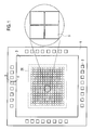
- a whole schematic plane pattern configuration of a solid state imaging device composed by arranging a photoelectric conversion device according to a first embodiment of the present invention in two dimensions includes: a package substrate 1; a plurality of bonding pads 2 disposed on the periphery on the package substrate 1; and an aluminum electrode layer 3 which is connected with the bonding pad 2 and a bonding pad connecting unit 4, and is connected to a transparent electrode layer 26 disposed on a pixel 5 of the solid state imaging device, on the periphery of the solid state imaging device. That is, the aluminum electrode layer 3 covers an end region of the transparent electrode layer 26, and the aluminum electrode layer 3 is connected to the one bonding pad 2 via the bonding pad connecting unit 4.
- the pixel 5 is disposed at matrix shape in the example of Fig. 1 .
- a schematic cross-section structure of the photoelectric conversion device according to the first embodiment of the present invention includes a circuit unit 30 formed on a substrate, and a photoelectric conversion unit 28 placed on the circuit unit 30.
- illustration of a lower electrode layer 25 and a buffer layer 36 is omitted.
- the photoelectric conversion device shown in Fig. 2 includes: a circuit unit 30 formed on the semiconductor substrate 10; a lower electrode layer 25 disposed on the circuit unit 30; a compound semiconductor thin film 24 of a chalcopyrite structure disposed on the lower electrode layer 25; a buffer layer 36 disposed on the compound semiconductor thin film 24; and a transparent electrode layer 26 disposed on the buffer layer 36.
- the lower electrode layer 25, the compound semiconductor thin film 24, the buffer layer 36, and the transparent electrode layer 26 are laminated one after another on the circuit unit 30.
- reverse bias voltage is applied between the transparent electrode layer 26 and the lower electrode layer 25, and the multiplication of electric charge generated by photoelectric conversion is made to generate by impact ionization within the compound semiconductor thin film 24 of chalcopyrite structure.
- the circuit unit 30 includes a transistor by which the lower electrode layer 25 is connected to the gate.
- the circuit unit 30, and the lower electrode layer 25, the compound semiconductor thin film 24, the buffer layer 36, and the transparent electrode layer 26 laminated one after another on the circuit unit 30 may be integrated.
- molybdenum (Mo), niobium (Nb), tantalum (Ta), tungsten (W), etc. can be used, for example.
- CdS, ZnS, ZnO, ZnMgO, ZnSe, In 2 S 3 , etc. can be used, for example.
- the transparent electrode layer 26 is composed of a non-doped ZnO film (i-ZnO) disposed on the compound semiconductor thin film 24, and an n type ZnO film disposed on the non-doped ZnO film (i-ZnO).
- i-ZnO non-doped ZnO film
- the photoelectric conversion device shown in Fig. 2 can also be composed as photosensor having sensitivity also in a near infrared optical wavelength region.
- the compound semiconductor thin film 24 includes the surface with the high resistivity layer (i type CIGS layer).
- the circuit unit 30 may include a Complementary Metal oxide Semicondudor Field Effect Transistor (CMOSFET), for example.
- CMOSFET Complementary Metal oxide Semicondudor Field Effect Transistor
- an n channel MOS transistor which composes a part of CMOS is shown in the circuit unit 30, and the circuit unit 30 includes: a semiconductor substrate 10; source/drain regions 12 formed in the semiconductor substrate 10; a gate insulating film 14 disposed on the semiconductor substrate 10 between the source/drain regions 12; a gate electrode 16 disposed on the gate insulating film 14; a VIA0 electrode 17 disposed on the gate electrode 16; a wiring layer 18 for gates disposed on the VIA0 electrode 17; and The VIA1 electrode 22 disposed on the wiring layer 18.
- All of the gate electrode 16, the VIA0 electrode 17, the wiring layer 18, and the VIA1 electrode 22 are formed in an interlayer insulating film 20.
- a VIA electrode 32 disposed on the gate electrode 16 is formed of the VIA0 electrode 17, the wiring layer 18 disposed on the VIA0 electrode 17, and the VIA1 electrode 22 disposed on the wiring layer 18.
- the gate electrode 16 and the photoelectric conversion unit 28 of a n channel MOS transistor which compose a part of CMOS are electrically connected by the VIA electrode 32 disposed on the gate electrode 16.
- an anode of a photo diode which composes the photoelectric conversion unit 28 is connected to the gate electrode 16 of the n channel MOS transistor, optical information detected in the photo diode is amplified by the aforementioned n channel MOS transistor.
- circuit unit 30 can also be formed by the thin film transistor of the CMOS structure formed on a thin film formed on a glass substrate, for example.
- Fig. 3 shows more detailed cross-sectional configuration chart including adjoining pixels of the solid state imaging device composed by arranging the photoelectric conversion device according to the first embodiment in two dimensions.
- the compound semiconductor thin film 24 disposed on the lower electrode layer 25 and the lower electrode layer 25 is separated each other via the isolation region 34 formed with the interlayer insulating film between adjoining pixel cells.
- the buffer layer 36 disposed on the compound semiconductor thin film 24 is formed in one piece all over the semiconductor substrate surface.
- the transparent electrode layer 26 is formed in one piece all over the semiconductor substrate surface, and is performed in common electrically.
- the width of the compound semiconductor thin film 24 and the width of the lower electrode layer 25 may be equivalent, or more for details, as shown in Fig. 3 , it may set to so that the width of the compound semiconductor thin film 24 may become larger than the width of the lower electrode layer 25.
- the void and pinhole which are occurred in an underlying CIGS thin film are embedded by a semi-insulating layer and leak can be prevented, by providing a non-doped ZnO film (i-ZnO) as the transparent electrode layer 26. Therefore, the dark current of the pn junction interface can be reduced by applying the non-doped ZnO film (i-ZnO) as a thick film.
- the configuration which has the buffer layer 36 as an embodiment is mentioned above.
- the leakage current can be reduced by the buffer layer 36
- the present invention is not limited to the configuration. It maybe the configuration of providing an electrode layer without the buffer layer on the compound semiconductor thin film (CIGS) layer.
- the photoelectric conversion unit 28 of the photoelectric conversion device includes: a lower electrode layer 25; a compound semiconductor thin film 24 disposed on the lower electrode layer 25; a buffer layer 36 disposed on the compound semiconductor thin film 24; a semi-insulating layer (iZnO layer) 261 disposed on the buffer layer 36; and an upper electrode layer (nZnO layer) 262 disposed on the semi-insulating layer (iZnO layer) 261.
- the void and pinhole which are occurred in the underlying CIGS thin film 24 are embedded by the semi-insulating layer and the leak can be prevented by forming the semi-insulating layer 261 which is composed of a non-doped ZnO layer as the transparent electrode layer 26.
- the ZnO layer composed of the semi-insulating layer (iZnO layer) 261 and the upper electrode layer (nZnO layer) 262 can also be composed only of the upper electrode layers (nZnO layer) 262.
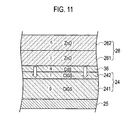
- an i type CIGS layer (high resistivity layer) 242 is formed in the interface which contacts the buffer layer 36 of the compound semiconductor thin film 24.
- the underlying CIGS thin film 241 is a p type
- the pin junction composed of the p type CIGS layer 241, the i type CIGS layer 242, and the n type buffer layer (CdS) 36 is formed as shown in Fig. 4(a) and Fig. 4(b) .
- the leak due to the tunnel current which occurs when the conductive upper electrode layer 262 is directly contacted to the CIGS thin film 24 can be prevented by the structure of the upper electrode layer (nZnO layer) 262/semi-insulating layer (iZnO layer) 261/buffer layer 36/i type CIGS layer 242/p type CIGS layer 241/lower electrode layer 25. Also, the dark current can be reduced by setting the semi-insulating layer 261 composed of the non-doped ZnO layer to thick film.
- the thickness of the upper electrode layer 262 is about 500 nm, for example, the thickness of the semi-insulating layer 261 is about 200 nm, for example, the thickness of the buffer layer 36 is about 100 nm, for example, the thickness of the i type CIGS layer 242 is about 200 nm to 600 nm, for example, the thickness of the p type CIGS layer 241 is about 1 to 2 ⁇ m, for example, and the thickness of the lower electrode layer 25 is about 600 nm, for example.
- the whole thickness from the lower electrode layer 25 to the transparent electrode layer 26 is about 3 ⁇ m, for example.
- the transparent electrode layer 26 other electrode materials are also applicable.
- an ITO film, a tin oxide (SnO 2 ) film, or an indium oxide (In 2 O 3 ) film can be used.
- Fig. 5(a) shows a configuration diagram of the compound semiconductor thin film which forms pin junction
- Fig. 5(b) shows a field strength distribution diagram corresponding to Fig. 5(a) .
- Fig. 6 is a diagram for explaining avalanche multiplication, a vertical axis shows the signal current I sj (A), and a horizontal axis shows target voltage V t (V) applied between the upper electrode layer and the lower electrode layer.
- the target voltage is made to increase, the signal current will increase dramatically. Accordingly, the sensitivity of the sensor can be improved.
- the target voltage V t equivalent to a reverse bias voltage of pin junction is applied between the upper electrode layer 262 composed of n type ZnO, and the lower electrode layer 25 by which ohmic contact was performed to the p type CIGS layer 241.
- the value of the peak value E1 of the electric field strength E (V/cm) is about 4 ⁇ 10 4 to 4 ⁇ 10 5 (V/cm).
- the value of E1 is changed according to the CIGS composition and the film thickness of the compound semiconductor thin film 24.
- the avalanche multiplication region in Fig. 6 is about 10V region as the target voltage V t .
- about 100V is necessary in the case of the usual silicone device.
- Fig. 7 shows current-voltage characteristics for explaining a multiplication phenomenon in the case with light irradiation and in the case without light irradiation.
- the change of the current value of is slight when the comparatively low target voltage V t is applied.
- the change of the current value of is very remarkable in the state where the high voltage is applied relatively and the avalanche multiplication operation may occur.
- the dark current in the case without light irradiation is substantially of the same grade, comparing P1 andA1. Therefore, in the photoelectric conversion device according to the first embodiment, it is obvious that the S/N ratio is also improved.
- the compound semiconductor thin film of chalcopyrite structure which functions as the optical absorption layer can be formed by the vacuum evaporation method called Physical Vapor Deposition (PVD), a sputtering technique, or Molecular Beam Epitaxy (MBE) on a semiconductor substrate or a glass substrate in which the circuit unit 30 is formed.
- PVD Physical Vapor Deposition
- MBE Molecular Beam Epitaxy
- the PVD shall mean the method of forming a film by making the primary material evaporated in the vacuum deposit.
- the vacuum evaporation method When using the vacuum evaporation method, it is made to vapor-deposit on the substrate in which the circuit unit 30 is formed, bymakingeachcomponent (Cu, In, Ga, Se, S) of the compound into a vacuum evaporation source independently.
- a chalcopyrite compound is used as a target or each the component is independently used as a target.
- the substrate is heated to high temperature when forming the compound semiconductor thin film of chalcopyrite structure on the glass substrate in which the circuit unit 30 is formed, the stoichiometry shift may occur by separation of a chalcogenide element.
- a formation process of the compound semiconductor thin film of the chalcopyrite structure applied to the fabrication method for the photoelectric conversion device according to the comparative example of the present invention is shown as a three-step method shown in Fig. 8 , for example.
- Fig. 8(a) shows the substrate temperature in each stap and the component at the time of forming the film by the sputtering technique.
- Fig. 8(b) shows the composition ratio in each stap (Cu/group III (In+Ga)).
- the composition ratio of (Cu/group III (In+Ga)) is remained 0, in the group III element is a rich state.
- the third step shifts from a rich state of Cu element of (Cu/group III (In+Ga)) whose composition ratio is more than 1.0 to a rich state of group III element of (Cu/group III (In+Ga)) whose composition ratio is not more than 1.0.
- the formation of the compound semiconductor thin film 24 is performed not more than about 400 degrees C. When the substrate temperature is high enough, each constituent element may be diffused mutually.
- Fig. 9 shows a schematic cross-sectional configuration chart of the photoelectric conversion unit formed by the fabrication method for the photoelectric conversion device according to the comparative example of the present invention.
- the fabrication method for the photoelectric conversion device according to the comparative example of the present invention since diffusion of Cd from the buffer layer 36 appears remarkably, the n type CIGS layer (not shown) formed by the diffusion layer of Cd in the buffer layer 36 side of the compound semiconductor thin film 24.
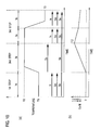
- Fig. 10 is a detailed explanation diagram of the formation process of the compound semiconductor thin film of chalcopyrite structure, and shows the component at the time of forming films by an evaporation method and the substrate temperature in each stap, in the fabrication method for the photoelectric conversion device according to the first embodiment.
- the Film formation may be performed by a sputtering technique.
- the third step forms the compound semiconductor thin film of chalcopyrite structure by having the first period (period 3a) that holds the substrate temperature to the second temperature T2, and the second period (period 3b) that holds the substrate temperature from the second temperature T2 to the third temperature T3 lower than the first temperature T1.
- the third temperature T3 is not less than about 300 degrees C and not more than degree 400 degrees C, for example.
- the second temperature is not more than about 550 degrees C, for example.
- the third step it is effective setting (Cu/ (In+Ga)) at the time of completing of the first step (period 3a) as a range of about 0.5 to 1.3, for example, and effective also setting (Cu/ (In+Ga)) at the time of completing of the second step (period 3b) as not more than 1.0 value.
- the compound semiconductor thin film 24 has the i type CIGS layer 242 on the surface.
- the first step and the second step are the same as the comparative example shown in Fig. 8(a)
- the third step is separated into two steps and is a high temperature process step of the temperature T2 during the 3a period, it shifts to the low temperature process step of the temperature T3, and the i type CIGS layer 242 is positively formed on the surface of the compound semiconductor thin film 24 in the 3b period.
- the substrate temperature is 300 degrees C to 400 degrees C, for example, and shall be about 300 degrees C.
- the vacuum evaporation of each component element is not vapor-deposited at the same time, but is separated and performed in three steps, and distribution of each component element in the film can be controlled to some extent.
- the beam flux of In element and Ga element is used for control of the bandgap of the compound semiconductor thin film 24.
- Cu/group III (In+Ga) ratio can be used for control of the Cu density in the CIGS film. Setting of Cu/group III (In+Ga) ratio is relatively easy. Control of film thickness is also easy. Se is always supplied in fixed quantity.
- the third step Cu/group III (In+Ga) ratio is reduced, and the i type CIGS layer 242 can be easily formed on the surface of the compound semiconductor thin film 24 with effective controllability of film thickness. It is considered that it functions as the i layer since the i type CIGS layer 242 has a low density of Cu which adjusts the carrier density in the film and there are few carriers.
- the present invention is not limited to the configuration.
- the process can once be completed after performing the three-step method, Cu fraction can be reduced with performing the temperature change to temperature as shown in the period 3b of Fig. 10 after that, and a desired CIGS surface layer can also be formed.
- the three-step method was explained as the example, the present invention is also not limited to the configuration.
- the present invention can also be performed using a bilayer method.
- the bilayer method is a method of forming the CIGS film by the evaporating method, a sputtering technique, etc.
- a desired CIGS surface layer can also be formed by reducing Cu fraction while changing the temperature to temperature as shown in the period 3b of Fig. 10 .
- the present invention can also be implemented by performing the still more above lower-temperature forming steps to the CIGS thin film created using other method for forming film (a sulfurating method, a seleniding/sulfurating method, a multi-source evaporation method, an in-line type multi-source evaporation method, a high-speed solid phase seleniding method, and a roll two roll (RR) method, an ionization vacuum evaporation and RR method, a multi-source evaporation and RR method, an electrodeposition method, a hybrid process, a hybrid sputtering and RR method, a nano particle printing method, a nano particle printing and RR method, anFASST (registeredtrademark) process).
- a sulfurating method a seleniding/sulfurating method, a multi-source evaporation method, an in-line type multi-source evaporation method, a high-speed solid phase seleniding method, and a roll two roll (RR) method,
- Fig. 11 shows a schematic cross-sectional configuration chart of the photoelectric conversion unit in the photoelectric conversion device formed by the fabrication method for the photoelectric conversion device according to the first embodiment.
- the fabrication method for the photoelectric conversion device according to the 1st embodiment in the third step in the three-step method mentioned abave, Cu/group III (In+Ga) ratio is reduced, and the i type CIGS layer 242 can be easily formed on the surface of the compound semiconductor thin film 24 with the effective controllability of film thickness. It also becomes possible easily to form the thickness of the i type CIGS layer 242 thinly.
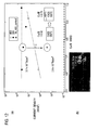
- Fig. 12(a) shows the relationship of the dark current density (A/cm 2 ) and Cu/group III ratio as a result which applied the fabrication method for the photoelectric conversion device to test structure.
- Fig. 12(b) shows the SEM photograph of an example of the test structure which laminated Mo and CIGS on the substrate.
- the dark current value is about 3.2 ⁇ 10 -7 (A/cm 2 ), and remarkable dependence is not observed even if it changes Cu/group III ratio.
- the dark current value is about 1.5 ⁇ 10 -8 (A/cm 2 ) to about 1 ⁇ 10 -7 (A/cm 2 ), and the tendency which increases gradually is observed as Cu/group III ratio is made to increase to about 0.6 to about 0.92.
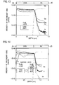
- Fig. 13 shows an analysis result by SIMS of the photoelectric conversion unit formed by the fabrication method for the photoelectric conversion device according to the comparative example of the present invention.
- the second step and the third step of substrate temperature are about 550 degrees C, and Cu/group III ratio is about 0.75 examples.
- reduction of Cu element is not observed in the surface of the compound semiconductor thin film 24. That is, the surface layer of the compound semiconductor thin film 24 is not formed into i type.
- Fig. 14 shows an analysis result by SIMS of the photoelectric conversion unit formed by the fabrication method for the photoelectric conversion device according to the first embodiment.
- the substrate temperature is about 400 degrees C in the second step and the period 3a of the third step, and is about 300 degrees C in the period 3b of the third step, remarkable reduction of Cu element is observed in 0.75 for Cu/group III ratio and on the surface of the compound semiconductor thin film 24. That is, the surface layer of the compound semiconductor thin film 24 is formed into i type, and the i type CIGS layer 242 is formed.
- the substrate temperature is set to about 400 degrees C in the second step, and Cu/group III ratio is set to 0.92.
- the substrate temperature is set to about 300 degrees C, and Cu/group III ratio is set to 0.75.
- the thickness of the surface layer (i type CIGS layer 242) of the compound semiconductor thin film 24 formed into i type is about 200 nm.
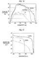
- Fig. 15 shows wavelength characteristic of the quantum efficiency which applies a parameter as the value of Cu/group III ratio of the compound semiconductor thin film (CIGS thin film) formed by the fabrication method for the photoelectric conversion device according to the first embodiment.
- the substrate temperature is set to about 400 degrees C in the second step and the period 3a of the third step, and is set to about 300 degrees C in the period 3b of the third step, as well as the case of Fig. 14 .
- the reduction tendency is observed as the value of Cu/group III ratio of the compound semiconductor thin film 24 reduces such as 0.9, 0.8, 0.6.
- the value of Cu/group III ratio of the compound semiconductor thin film 24 reduces such as 0.9, 0.8, 0.6 corresponding to reduce the Cu fraction by lengthening the period 3b, since the thickness of the surface layer (i type CIGS layer 242) of the compound semiconductor thin film 24 formed into i type becomes thick and the quantum ef f iciency at the side of short wavelength reduces.
- the quantum efficiency is not less than double compared with the photoelectric conversion characteristic in the case of silicon (Si).
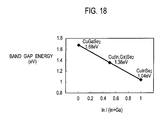
- the bandgap energy of Cu(Ga)Se 2 is 1.68 eV
- the bandgap energy of Cu(In, Ga)Se 2 is 1.38 eV
- the bandgap energy of Cu(In)Se 2 is 1.04 eV.
- the photoelectric conversion wavelength can be applied variable by composition control.
- the dark current reduction it may be applied Ga rich near the top surface and the bottom surface of the CIGS film, and thereby the bandgap energymaybe decreased.
- it maybe applied In rich and bandgap energy may be applied small in the range of the predetermined depth in a CIGS film.
- Fig. 19 shows the relationship between the dark current (A/cm 2 ) and the temperature for forming surface layer T A (degrees C) of the photoelectric conversion device formed by the fabrication method for the photoelectric conversion device according to the first embodiment of the present invention.
- the dark current characteristics will improve. Even if it reduces the temperature for forming surface layer T A from about 400 degrees C to about 300 degrees C, for example, the dark current characteristics improve.
- the temperature for forming surface layer T A is set to not more than about 300 degrees C, for example, the value of dark current rises and the dark current characteristics deteriorate.
- Fig. 20(a) shows an example of Scanning Capacitance Microscope (SCN) photograph of the photoelectric conversion unit of the photoelectric conversion device formed by the fabrication method for the photoelectric conversion device according to the comparative example of the first embodiment.
- Fig. 20(b) shows an explanatory diagram of Fig. 20(a) .
- the pn junction composed of the p type CIGS layer 241 and the n type buffer layer (CdS) 36 is formed in the photoelectric conversion unit of the photoelectric conversion device according to the comparative example as well as that of Fig. 9 .
- the region which the dC/dV signal is not outputting in the boundary of the p type CIGS layer 241 and the n type buffer layer (CdS) 36 indicates a bonding depletion layer having the width d1.
- the region which becomes n type in the wide range in the p type CIGS layer 241 is observed (not shown in Fig. 20(b) ). Such a region is considered to have contributed to the leak path accompanied by the increase in the dark current.
- Fig. 21(a) shows an example of SCN photograph of the photoelectric conversion unit of the photoelectric conversion device formed by the fabrication method for the photoelectric conversion device according to the first embodiment.
- Fig. 21(b) shows an explanatory diagram of Fig. 21(a) .
- the pin junction composed of the p type CIGS layer 241 and the n type buffer layer (CdS) 36 is formed in the photoelectric conversion unit of the photoelectric conversion device according to the first embodiment as well as that of Fig. 11 .
- the region which the dC/dV signal is not outputting in the boundary of the p type CIGS layer 241 and the n type buffer layer (CdS) 36 indicates a bonding depletion layer having the width d2. According to the first embodiment, most regions reversed to the n type in the p type CIGS layer 241 are not observed. Therefore, it is considered that the leak path accompanied by the increase in the dark current does not exist, but is contributed to the improvement of dark current characteristics.
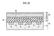
- a solid state imaging device composed by applying the photoelectric conversion device according to the first embodiment of the present invention includes: a circuit unit 30 formed on the semiconductor substrate 10, and a photoelectric conversion unit 28 disposed on the circuit unit 30 as shown in Fig. 22 as a cross-sectional diagram of one pixel part. In addition, in Fig. 22 , illustrationof abufferlayer36 is omitted.
- the solid state imaging device shown in Fig. 22 includes: a circuit unit 30 formed on the semiconductor substrate 10; a lower electrode layer 25 disposed on the circuit unit 30 and mutually separated between the pixels adjoining to a column direction or a row direction; a compound semiconductor thin film 24 of the chalcopyrite structure disposed on the lower electrode layer 25 and mutually separated between the pixels adjoining to a column direction or a row direction; a buffer layer 36 disposed on the compound semiconductor thin film 24; a transparent electrode layer 26 disposed on the buffer layer 36.
- the column direction is a direction to extend a bit line which reads a signal of each pixel
- a row direction is a direction to intersect perpendicularly in the column direction and to extend a word line which is an address line to each pixel.
- the lower electrode layer 25, the compound semiconductor thin film 24, the buffer layer 36, and the transparent electrode layer 26 are laminated one after another on the circuit unit 30.
- the reverse bias voltage is applied between the transparent electrode layer 26 and the lower electrode layer 25, and the multiplication of electric charge generated by photoelectric conversion is made to generate by impact ionization within the compound semiconductor thin film 24 of chalcopyrite structure.
- the circuit unit 30 includes a transistor by which the lower electrode layer 25 is connected to the gate.
- the circuit unit 30, and the lower electrode layer 25, the compound semiconductor thin film 24, the buffer layer 36, and the transparent electrode layer 26 laminated one after another on the circuit unit 30 may be integrated.
- molybdenum (Mo), niobium (Nb), tantalum (Ta), tungsten (W), etc. can be used, for example.
- CdS, ZnS, ZnO, ZnMgO, ZnSe, In 2 S 3 , etc. can be used, for example.
- the solid state imaging device shown in Fig. 22 can also be composed as an image sensor having sensitivity also in a near infrared optical wavelength region.
- the solid state imaging device shown in Fig. 22 may include a color filter on the transparent electrode layer 26.
- the color filter is effective also as one at 3 couples by providing for red, green, and blue in the adjoining pixels 5. It is effective also as one at 4 couples by adding the filter for near-infrared rays. These 4 couples may be disposed in the matrix shape of 2 ⁇ 2.
- the color filter can also be formed by multilayering of a gelatin film, for example.
- the gate electrode 16 and the photoelectric conversion unit 28 of the n channel MOS transistor which compose a part of CMOS are electrically connected by the VIA electrode 32 disposed on the gate electrode 16.
- an anode of a photo diode which composes the photoelectric conversion unit 28 is connected to the gate electrode 16 of the n channel MOS transistor, optical information detected in the photo diode is amplified by the aforementioned n channel MOS transistor.
- the configuration which has the buffer layer 36 as the embodiment is mentioned above.
- the leakage current can be reduced by the buffer layer 36
- the present invention is not limited to the configuration. It may be a configuration of providing an electrode layer without the buffer layer on the compound semiconductor thin film (CIGS) layer.
- a circuit configuration of one pixel C ij of the solid state imaging device composed by applying the photoelectric conversion device according to the first embodiment is expressed by photo diode PD and three MOS transistors, for example, as shown in Fig. 23(a) .
- a circuit configuration of one pixel C ij of the solid state imaging device according to the comparative example of the present invention is shown, for example, as shown in Fig. 23(b) .
- the solid state imaging device composed by applying the photoelectric conversion device according to the first embodiment, in order to apply the high voltage of reverse bias between the anode and cathode of photo diode PD, it is necessary to use a circuit configuration different from the circuit configuration of one pixel C ij of the solid state imaging device according to the comparative example to which the relatively low voltage is applied.
- a photoelectric conversion cell composed of the circuit unit 30 and the photoelectric conversion unit 28 is integrated by one-dimensional matrix shape or two-dimensional matrix shape.
- the matrix of 3 ⁇ 3 in the configuration example of Fig. 24 , it is extensible to the matrix of m ⁇ n as mentioned above.
- the circuit configuration of each pixel shown in Fig. 24 corresponds to Fig. 23(a) .
- the buffer 100 is a source follower surrounded with the dashed line of Fig. 23(a) , and is composed of the constant current source Ic and MOS transistor M SF .
- the gate of select MOS transistor M SEL is connected to the word line WL.
- Target voltage V t (V) is applied to the cathode of photo diode PD.
- the capacitor C PD is a depletion layer capacitance of photo diode PD, and is a capacitor for performing the charge storage.
- MOS transistor M SF for source follower The drain of MOS transistor M SF for source follower is connected to the power supply voltage V DDPD .
- the anode of photo diode PD is connected to MOS transistor M RST for reset, and the photo diode PD is reset by the initial state at the timing of the signal inputted into the reset terminal RST.
- circuit unit 30 is shown by the example of the semiconductor integrated circuit placed on the semiconductor substrate 10 in the example of Fig. 22 , the circuit unit 30 canal so be formed with the thin film transistor integrated circuit which integrates the thin film transistor formed on the thin film formed on the glass substrate, for example.
- the compound semiconductor thin film 24 disposed on the lower electrode layer 25 is separated mutually via the isolation region 34, between adjoining pixel cells.
- the buffer layer 36 disposed on the compound semiconductor thin film 24 and the isolation region 34 is formed in one piece all over the semiconductor substrate surface.
- a gate insulating film disposed on the semiconductor substrate 10 between source/drain regions 12 is omitting illustration.
- a VIA electrode 32 embedded in an interlayer insulating film 20 is disposed between the gate electrode 16 and the lower electrode layer 25.
- the transparent electrode layer 26 is formed on the semiconductor substrate surface in one piece, and is performed in common electrically.
- the transparent electrode layer 26 becomes a cathode electrode of the photo diode (PD) which composes the photoelectric conversion unit 28, and is made by the constant potential (target voltage V t ) for applying a high electric field. Therefore, in a plurality of integrated pixels, it is not necessary to perform isolation formation of the cathode electrode of the photo diode (PD) which composes the photoelectric conversion unit 28, and it is formed on the semiconductor substrate surface in one piece, and is performed in common electrically.
- the whole pixel region of the photoelectric conversion cell is usable as a substantial photoelectric conversion region. Accordingly, in the CMOS type image sensor, the optical aperture is about 80 to about 90% compared with about 30 to about 40% of the optical aperture at the time of forming in the semiconductor substrate by applying the photoelectric conversion unit 28 as a pn junction diode, and it has a large improvement effect.
- the transparent electrode layer (ZnO film) 26 becomes equipotential, it is not necessary to perform isolation formationof the transparent electrode layer (ZnO film) 26 for every pixel, the electrode composed of aluminum etc. may be disposed to be meshed shaped or stripe shaped on the transparent electrode layer in a fixed pitch, in the range which does not have on the optical aperture of a pixel, in the case of the large capacity area sensor etc. with which specific resistance becomes a problem.
- the photoelectric conversion device of high S/N ratio which improved detection efficiency substantially also with low illumination, and the fabrication method for such photoelectric conversion device, and a solid state imaging device, by applying the high electric field to the photoelectric conversion unit which used the chalcopyrite type semiconductor, and generating the multiplication of the electric charge by impact ionization and improving dark current characteristics.
- the first embodiment can provide of the photoelectric conversion device which the multiplication phenomenonnot observed conventional can be observed by improving dark current characteristics, and can also be detected in the light of low illumination, and the fabrication method for such photoelectric conversion device.
- the solid state imaging device of high S/N ratio which improved detection efficiency substantially also with low illumination, by applying the high electric field to the photoelectric conversion unit which used the chalcopyrite type semiconductor, and generating the multiplication of the electric charge by impact ionization and improving dark current characteristics.
- the solid state imaging device which the multiplication phenomenon not observed conventional can be observed by improving dark current characteristics, and can also be detected in the light of low illumination.
- a whole schematic plane pattern configuration of a solid state imaging device composed by arranging a photoelectric conversion device according to a second embodiment of the present invention in two dimensions is the same as that of Fig. 1 . Therefore, the explanation is omitted.
- a schematic cross-section structure of the photoelectric conversion device according to the second embodiment of the present invention includes a circuit unit 30 formed on a substrate, and a photoelectric conversion unit 28 disposed on the circuit unit 30.
- a lower electrode layer 25 and a buffer layer 36 is omitted.
- the photoelectric conversion device shown in Fig. 25 includes: a circuit unit 30 formed on the semiconductor substrate 10; a lower electrode layer 25 disposed on the circuit unit 30; a compound semiconductor thin film 24 of a chalcopyrite structure disposed on the lower electrode layer 25; a buffer layer 36 disposed on the compound semiconductor thin film 24; and a transparent electrode layer 26 disposed on the buffer layer 36.
- the lower electrode layer 25, the compound semiconductor thin film 24, the buffer layer 36, and the transparent electrode layer 26 are laminated one after another on the circuit unit 30.
- reverse bias voltage is applied between the transparent electrode layer 26 and the lower electrode layer 25, and the multiplication of electric charge generated by photoelectric conversion is made to generate by impact ionization within the compound semiconductor thin film 24 of chalcopyrite structure.
- the circuit unit 30 includes a transistor by which the lower electrode layer 25 is connected to a source or a drain.
- the circuit unit 30, and the lower electrode layer 25, the compound semiconductor thin film 24, the buffer layer 36, and the transparent electrode layer 26 laminated one after another on the circuit unit 30 may be integrated.
- molybdenum (Mo), niobium (Nb), tantalum (Ta), tungsten (W), etc. can be used, for example.
- CdS, ZnS, ZnO, ZnMgO, ZnSe, In 2 S 3 , etc. can be used, for example.
- the transparent electrode layer 26 is composed of a non-doped ZnO film (i-ZnO) disposedon the compound semiconductor thin film 24, and an n type ZnO film disposed on the non-doped ZnO film (i-ZnO).
- i-ZnO non-doped ZnO film
- the photoelectric conversion device shown in Fig. 25 can also be composed as a photosensor having sensitivity also in a near infrared optical wavelength region.
- the compound semiconductor thin film 24 includes the surface with a high resistivity layer (i type CIGS layer).
- an n channel MOS transistor which composes a part of CMOS is shown in the circuit unit 30, and the circuit unit 30 includes: a semiconductor substrate 10; source/drain regions 12 formed in the semiconductor substrate 10; a gate insulating film 14 disposed on the semiconductor substrate 10 between the source/drain regions 12 ; a gate electrode 16 disposed on the gate insulating film 14; a VIA0 electrode 17 disposed on the source/drain region 12, a wiring layer 18 for source/drain disposed on the VIA0 electrode 17, and a VIA1 electrode 23 disposed on the wiring layer 18.
- All of the gate electrode 16, the VIA0 electrode 17, the wiring layer 18, and the VIA1 electrode 23 are formed in an interlayer insulating film 20.
- a VIA electrode 33 disposed on the source/drain region 12 is formed of the VIA0 electrode 17, the wiring layer 18 disposed on the VIA0 electrode 17, and the VIA1 electrode 23 disposed on the wiring layer 18.
- the source/drain region 12 and the photoelectric conversion unit 28 of the n channel MOS transistor which compose a part of the CMOS are electrically connected via the VIA electrode 33 disposed on the source/drain region 12.
- FIG. 3 More detailed cross-sectional configuration chart including adjoining pixels of the solid state imaging device composed by arranging the photoelectric conversion device according to the second embodiment in two dimensions is similarly expressed as Fig. 3 .
- Fig. 3 it corresponds to the case of providing the VIA electrode 33 instead of the VIA electrode 32.
- the compound semiconductor thin film 24 disposed on the lower electrode layer 25 and the lower electrode layer 25 is separated each other via the isolation region 34 formed with the interlayer insulating film between adjoining pixel cells.
- the buffer layer 36 disposed on the compound semiconductor thin film 24 is formed in one piece all over the semiconductor substrate surface.
- the transparent electrode layer 26 is formed in one piece all over the semiconductor substrate surface, and is performed in common electrically.
- the width of the compound semiconductor thin film 24 and the width of the lower electrode layer 25 may be equivalent, or more for details, as shown in Fig. 3 , it may set to so that the width of the compound semiconductor thin film 24 may become larger than the width of the lower electrode layer 25.
- the void and pinhole which are occurred in an underlying CIGS thin film are embedded by a semi-insulating layer and the leak can be prevented, by providing a non-doped ZnO film (i-ZnO) as the transparent electrode layer 26. Therefore, the dark current of the pn junction interface can be reduced by applying the non-doped ZnO film (i-ZnO) as a thick film.
- the optical information detected in the photo diode is switched by the n channel MOS transistor.
- circuit unit 30 can also be formed by the thin film transistor of the CMOS structure formed on a thin film formed on a glass substrate, for example.
- the configuration which has the buffer layer 36 as the embodiment is mentioned above.
- the leakage current can be reduced by the buffer layer 36
- the present invention is not limited to the configuration. It may be a configuration of providing an electrode layer without the buffer layer on the compound semiconductor thin film (CIGS) layer.
- a solid state imaging device composed by applying the photoelectric conversion device according to the second embodiment of the present invention includes: a circuit unit 30 formed on the substrate 10, and a photoelectric conversion unit 28 disposed on the circuit unit 30 as shown in Fig. 26 as a cross-sectional diagram of one pixel part. In addition, in Fig. 26 , illustration of a buffer layer 36 is omitted.
- the solid state imaging device shown in Fig. 26 includes: a circuit unit 30 formed on the semiconductor substrate 10; a lower electrode layer 25 disposed on the circuit unit 30 and mutually separated between the pixels adjoining to a column direction or a row direction; a compound semiconductor thin film 24 of the chalcopyrite structure disposed on the lower electrode layer 25 and mutually separated between the pixels adjoining to a column direction or a row direction; a buffer layer 36 disposed on the compound semiconductor thin film 24; and a transparent electrode layer disposed on the buffer layer 36 and having planarization structure between the adjoining pixels
- the column direction is a direction to extend a bit line which reads a signal of each pixel
- the row direction is a direction to intersect perpendicularly in the column direction and to extend a word line which is an address line to each pixel.
- the lower electrode layer 25, the compound semiconductor thin film 24, the buffer layer 36, and the transparent electrode layer 26 are laminated one after another on the circuit unit 30.
- the reverse bias voltage is appliedbetween the transparent electrode layer 26 and the lower electrode layer 25, and the multiplication of electric charge generated by photoelectric conversion is made to generate by impact ionization within the compound semiconductor thin film 24 of chalcopyrite structure.
- the circuit unit 30 includes a transistor by which the lower electrode layer 25 is connected to a source or a drain.
- the circuit unit 30, and the lower electrode layer 25, the compound semiconductor thin film 24, the buffer layer 36, and the transparent electrode layer 26 laminated one after another on the circuit unit 30 may be integrated.
- molybdenum (Mo), niobium (Nb), tantalum (Ta), tungsten (W), etc. can be used, for example.
- CdS, ZnS, ZnO, ZnMgO, ZnSe, In 2 S 3 , etc. can be used, for example.
- the solid state imaging device shown in Fig. 26 can also be composed as an image sensor having sensitivity also in a near infrared optical wavelength region.
- the solid state imaging device shown in Fig. 26 may include a color filter on the transparent electrode layer 26.
- the color filter is effective also as one at 3 couples by providing for red, green, and blue in the adjoining pixels 5. It is effective also as one at 4 couples by adding the filter for near-infrared rays. These 4 couples may be disposed in the matrix shape of 2 ⁇ 2.
- the color filter can also be formed by multilayering of a gelatin film, for example.
- the source/drain region 12 and the photoelectric conversion unit 28 of the n channel MOS transistor which compose a part of the CMOS are electrically connected via the VIA electrode 33 disposed on the source/drain region 12.
- the optical information detected in the photo diode is switched by the n channel MOS transistor.
- circuit configuration of one pixel C ij of the solid state imaging device composed by applying the photoelectric conversion device according to the second embodiment also differs in the circuit configuration from Fig. 23(a) , it is expressed by photo diode PD and three MOS transistors (not shown). Also in the solid state imaging device composed by applying the photoelectric conversion device according to the second embodiment, in order to apply the high voltage of reverse bias between the anode and cathode of photo diode PD, it is necessary to use a circuit configuration different from the circuit configuration of one pixel C ij of the solid state imaging device according to the comparative example to which the relatively low voltage is applied.
- a photoelectric conversion cell composed of the circuit unit 30 and the photoelectric conversion unit 28 is integrated by one-dimensional matrix shape or two-dimensional matrix shape.
- the solid state imaging device composed by applying the photoelectric conversion device according to the second embodiment differs in the circuit configuration of each pixel C ij
- the matrix of 3 ⁇ 3 in the configuration example of Fig. 24 , it is extensible to the matrix of mxn as above-mentioned.
- circuit unit 30 is shown by the example of the semiconductor integrated circuit disposed on the semiconductor substrate 10 in the example of Fig. 26 , the circuit unit 30 canal so be formed with the thin film transistor integrated circuit which integrates the thin film transistor formed on the thin film formed on the glass substrate, for example.
- the compound semiconductor thin film 24 disposed on the lower electrode layer 25 is separated mutually via the isolation region 34, between adjoining pixel cells.
- the buffer layer 36 disposed on the compound semiconductor thin film 24 and the isolation region 34 is formed in one piece all over the semiconductor substrate surface.
- the VIA electrode 33 is disposed between the source/drain region 12 and the lower electrode layer 25.
- the transparent electrode layer 26 is formed by planarizing on the semiconductor substrate surface in one piece, and is performed in common electrically.
- the transparent electrode layer 26 becomes a cathode electrode of the photo diode (PD) which composes the photoelectric conversion unit 28, and is made by the constant potential (for example, target voltage V t ) for applying a high electric field. Therefore, inapluralityof integratedpixels, it is not necessary to perform isolation formation of the cathode electrode of the photo diode (PD) which composes the photoelectric conversion unit 28, and it is formed on the semiconductor substrate surface in one piece, and is performed in common electrically.
- V t target voltage
- the whole pixel region of the photoelectric conversion cell is usable as a substantial photoelectric conversion region. Accordingly, in the CMOS type image sensor, the optical aperture is about 80 to about 90% compared with about 30 to about 40% of the optical aperture at the time of forming in the semiconductor substrate by applying the photoelectric conversion unit 28 as a pn junction diode, and it has a large improvement effect.
- the transparent electrode layer (ZnO film) 26 becomes equipotential, it is not necessary to perform isolation formation of the transparent electrode layer (ZnO film) 26 for every pixel, the electrode composed of aluminum etc. may be disposed to be meshed shaped or stripe shaped on the transparent electrode layer (ZnO film) 26 in a fixed pitch, in the range which does not have on the optical aperture of a pixel, in the case of the large capacity area sensor etc. with which specific resistance becomes a problem.
- the configuration which has the buffer layer 36 as the embodiment is mentioned above.
- the leakage current can be reduced by the buffer layer 36
- the present invention is not limited to the configuration. It may be a configuration of providing an electrode layer without the buffer layer on the compound semiconductor thin film (CIGS) layer.
- the second embodiment can provide of the photoelectric conversion device of high S/N ratio which improved detection efficiency substantially also with low illumination, and the fabrication method for such photoelectric conversion device, and a solid state imaging device, by applying the high electric field to the photoelectric conversion unit which used the chalcopyrite type semiconductor, and generating the multiplication of the electric charge by impact ionization and improving dark current characteristics.
- the second embodiment can provide of the photoelectric conversion device which the multiplication phenomenon not observed conventional can be observed by improving dark current characteristics, and can also be detected in the light of low illumination, and the fabrication method for such photoelectric conversion device.
- the second embodiment can provide of the solid state imaging device of high S/N ratio which improved detection efficiency substantially also with low illumination, by applying the high electric field to the photoelectric conversion unit which used the chalcopyrite type semiconductor, and generating the multiplication of the electric charge by impact ionization and improving dark current characteristics.
- the second embodiment can provide the solid state imaging device which the multiplication phenomenon not observed conventional can be observed by improving dark current characteristics, and can also be detected in the light of low illumination.
- compound semiconductor thin film of the chalcopyrite structure can apply other compound semiconductorthinfilms, such as CuAlS 2 , CuAlSe 2 , CuAlTe 2 , CuGaS 2 , CuGaSe 2 , CuGaTe 2 , CuInS 2 , CuInSe 2 , CuInTe 2 , AgAlS 2 , AgAlSe 2 , AgAlTe 2 , AgGaS 2 , AgGaSe 2 , AgGaTe 2 , AgInS 2 , AgInSe 2 , AgInTe 2 , etc.
- compound semiconductorthinfilms such as CuAlS 2 , CuAlSe 2 , CuAlTe 2 , CuGaS 2 , CuGaSe 2 , CuGaTe 2 , CuInS 2 , CuInSe 2 , AgInTe 2 , etc.
- the present invention is not limited to the configuration. It may be a configuration of providing an electrode layer without the buffer layer on the compound semiconductor thin film (CIGS) layer.
- CGS compound semiconductor thin film
- the photoelectric conversion device and the solid state imaging device of the present invention have high sensitivity also in the near infrared light wavelength region, and therefore are applicable to an image sensor for a security camera (camera which performs sensing of the visible light at daytime and performs sensing of the near infrared light wavelength region at night), a personal authentication camera (camera for performing personal authentication with the near infrared light wavelength region which is not affected by an influence of outdoor daylight) or an in-vehicle camera (camera mounted in a car for visual aid at night, distant visual field securing, etc.), and also an image sensor detecting for near infrared light application of medical application and a photodetection device (photodetector) in a wide wavelength region, an avalanche photodiode, etc.
- a security camera camera which performs sensing of the visible light at daytime and performs sensing of the near infrared light wavelength region at night
- a personal authentication camera camera for performing personal authentication with the near infrared light wavelength
Landscapes
- Light Receiving Elements (AREA)
- Solid State Image Pick-Up Elements (AREA)
Applications Claiming Priority (2)
| Application Number | Priority Date | Filing Date | Title |
|---|---|---|---|
| JP2008104052A JP2009259872A (ja) | 2008-04-11 | 2008-04-11 | 光電変換装置およびその製造方法、および固体撮像装置 |
| PCT/JP2009/056523 WO2009125688A1 (fr) | 2008-04-11 | 2009-03-30 | Dispositif de conversion photoélectrique, procédé de fabrication de celui-ci, et dispositif d'imagerie à semi-conducteur |
Publications (1)
| Publication Number | Publication Date |
|---|---|
| EP2273565A1 true EP2273565A1 (fr) | 2011-01-12 |
Family
ID=41161820
Family Applications (1)
| Application Number | Title | Priority Date | Filing Date |
|---|---|---|---|
| EP09731141A Withdrawn EP2273565A1 (fr) | 2008-04-11 | 2009-03-30 | Dispositif de conversion photoélectrique, procédé de fabrication de celui-ci, et dispositif d'imagerie à semi-conducteur |
Country Status (4)
| Country | Link |
|---|---|
| US (1) | US8592933B2 (fr) |
| EP (1) | EP2273565A1 (fr) |
| JP (1) | JP2009259872A (fr) |
| WO (1) | WO2009125688A1 (fr) |
Cited By (4)
| Publication number | Priority date | Publication date | Assignee | Title |
|---|---|---|---|---|
| WO2011090959A3 (fr) * | 2010-01-21 | 2012-05-10 | Aqt Solar, Inc. | Contrôle de profils de composition dans des absorbeurs cigs recuits |
| EP2398054A3 (fr) * | 2010-06-18 | 2013-06-12 | Sony Corporation | Dispositif d'imagerie à l'état solide et son procédé de fabrication |
| WO2014103239A1 (fr) * | 2012-12-25 | 2014-07-03 | Sony Corporation | Dispositif capteur d'image à semi-conducteurs et appareil électronique |
| CN104377214A (zh) * | 2013-08-15 | 2015-02-25 | 索尼公司 | 摄像元件和摄像装置 |
Families Citing this family (21)
| Publication number | Priority date | Publication date | Assignee | Title |
|---|---|---|---|---|
| JP5609119B2 (ja) * | 2009-01-21 | 2014-10-22 | ソニー株式会社 | 固体撮像装置、その製造方法および撮像装置 |
| US20120217498A1 (en) * | 2009-09-01 | 2012-08-30 | Rohm Co., Ltd. | Photoelectric converter and method for manufacturing the same |
| JP2011151271A (ja) * | 2010-01-22 | 2011-08-04 | Rohm Co Ltd | 光電変換装置およびその製造方法、および固体撮像装置 |
| JP5536488B2 (ja) * | 2010-02-22 | 2014-07-02 | ローム株式会社 | カラー用固体撮像装置 |
| JP2012009707A (ja) * | 2010-06-25 | 2012-01-12 | Casio Comput Co Ltd | 光センサー及び光センサーの製造方法 |
| JP2012019169A (ja) * | 2010-07-09 | 2012-01-26 | Panasonic Corp | 固体撮像装置 |
| US9136184B2 (en) | 2011-02-18 | 2015-09-15 | Alliance For Sustainable Energy, Llc | In situ optical diagnostic for monitoring or control of sodium diffusion in photovoltaics manufacturing |
| JP5782768B2 (ja) * | 2011-03-23 | 2015-09-24 | セイコーエプソン株式会社 | 光電変換装置およびその製造方法 |
| JPWO2013190759A1 (ja) * | 2012-06-21 | 2016-02-08 | パナソニックIpマネジメント株式会社 | 固体撮像素子及びその製造方法 |
| KR101369166B1 (ko) * | 2012-07-13 | 2014-03-24 | 한국에너지기술연구원 | 태양전지용 cigs 광흡수층 형성 방법 및 cigs 태양전지 |
| JP6317877B2 (ja) * | 2012-10-16 | 2018-04-25 | ローム株式会社 | 光電変換装置および光電変換装置の製造方法 |
| JP2015061062A (ja) * | 2013-09-20 | 2015-03-30 | 株式会社東芝 | 光電変換素子の製造方法 |
| JP2015119018A (ja) * | 2013-12-18 | 2015-06-25 | ソニー株式会社 | 固体撮像素子および電子機器 |
| JP6451059B2 (ja) * | 2014-02-28 | 2019-01-16 | セイコーエプソン株式会社 | 光電変換装置、光電変換装置の製造方法及び電子機器 |
| WO2017081847A1 (fr) * | 2015-11-12 | 2017-05-18 | パナソニックIpマネジメント株式会社 | Dispositif de détection de lumière |
| US9923013B1 (en) * | 2016-11-18 | 2018-03-20 | Taiwan Semiconductor Manufacturing Company Ltd. | Sensor device, image sensor array and manufacturing method of sensor device |
| CN107731943B (zh) * | 2017-10-12 | 2019-03-01 | 宝应电工厂 | 一种铜铟镓基光电探测器 |
| JP6540780B2 (ja) * | 2017-12-12 | 2019-07-10 | ソニー株式会社 | 撮像素子および撮像装置 |
| CN108470783B (zh) * | 2018-03-28 | 2020-12-01 | 京东方科技集团股份有限公司 | 感光元件及其制造方法、显示面板及其制造方法 |
| JP7240833B2 (ja) * | 2018-08-01 | 2023-03-16 | 日本放送協会 | 撮像素子 |
| KR102291130B1 (ko) * | 2018-12-28 | 2021-08-18 | 한국에너지기술연구원 | Cigs 박막형 광흡수층의 제조방법, 이를 이용한 박막 태양 전지 제조방법 및 이에 의해 제조된 박막 태양 전지 |
Family Cites Families (27)
| Publication number | Priority date | Publication date | Assignee | Title |
|---|---|---|---|---|
| JPS6286856A (ja) * | 1985-10-14 | 1987-04-21 | Fuji Photo Film Co Ltd | 固体撮像素子の製造方法 |
| JPH0242769A (ja) * | 1988-08-03 | 1990-02-13 | Matsushita Electric Ind Co Ltd | pinフォトダイオードの製造方法 |
| US5436204A (en) * | 1993-04-12 | 1995-07-25 | Midwest Research Institute | Recrystallization method to selenization of thin-film Cu(In,Ga)Se2 for semiconductor device applications |
| US5441897A (en) | 1993-04-12 | 1995-08-15 | Midwest Research Institute | Method of fabricating high-efficiency Cu(In,Ga)(SeS)2 thin films for solar cells |
| JP3431388B2 (ja) * | 1995-03-15 | 2003-07-28 | 松下電器産業株式会社 | カルコパイライト構造半導体薄膜の製造方法 |
| US5918111A (en) * | 1995-03-15 | 1999-06-29 | Matsushita Electric Industrial Co., Ltd. | Method and apparatus for manufacturing chalcopyrite semiconductor thin films |
| JP3244408B2 (ja) * | 1995-09-13 | 2002-01-07 | 松下電器産業株式会社 | 薄膜太陽電池及びその製造方法 |
| JPH0982932A (ja) * | 1995-09-20 | 1997-03-28 | Hitachi Ltd | 固体撮像素子 |
| JPH09102627A (ja) * | 1995-10-06 | 1997-04-15 | Canon Inc | 光電変換装置 |
| JP2001144279A (ja) | 1999-11-12 | 2001-05-25 | Sony Corp | 固体撮像素子 |
| JP2002329877A (ja) * | 2001-04-27 | 2002-11-15 | National Institute Of Advanced Industrial & Technology | Cu(Ga及び(又は)In)Se2薄膜層、Cu(InGa)(S、Se)2薄膜層、太陽電池、Cu(Ga及び(又は)In)Se2薄膜層の形成方法 |
| US6500733B1 (en) * | 2001-09-20 | 2002-12-31 | Heliovolt Corporation | Synthesis of layers, coatings or films using precursor layer exerted pressure containment |
| US6635307B2 (en) * | 2001-12-12 | 2003-10-21 | Nanotek Instruments, Inc. | Manufacturing method for thin-film solar cells |
| JP3897622B2 (ja) * | 2002-03-18 | 2007-03-28 | 松下電器産業株式会社 | 化合物半導体薄膜の製造方法 |
| US20060060237A1 (en) * | 2004-09-18 | 2006-03-23 | Nanosolar, Inc. | Formation of solar cells on foil substrates |
| JP2005268479A (ja) * | 2004-03-18 | 2005-09-29 | Fuji Film Microdevices Co Ltd | 光電変換膜積層型固体撮像装置 |
| DE112005000785T5 (de) * | 2004-04-09 | 2007-03-01 | Honda Motor Co., Ltd. | Verfahren zur Herstellung einer Licht-absorbierenden Schicht für eine Dünnschichtsolarzelle des Chalkopyrittyps |
| JP2006049768A (ja) * | 2004-08-09 | 2006-02-16 | Showa Shell Sekiyu Kk | Cis系化合物半導体薄膜太陽電池及び該太陽電池の光吸収層の製造方法 |
| JP2006186118A (ja) * | 2004-12-28 | 2006-07-13 | Sony Corp | 固体撮像素子、固体撮像素子の製造方法および撮像装置 |
| KR100775058B1 (ko) * | 2005-09-29 | 2007-11-08 | 삼성전자주식회사 | 픽셀 및 이를 이용한 이미지 센서, 그리고 상기 이미지센서를 포함하는 이미지 처리 시스템 |
| JP2007123720A (ja) | 2005-10-31 | 2007-05-17 | Rohm Co Ltd | 光電変換装置およびその製造方法 |
| JP2007123721A (ja) | 2005-10-31 | 2007-05-17 | Rohm Co Ltd | 光電変換装置の製造方法および光電変換装置 |
| US8299510B2 (en) * | 2007-02-02 | 2012-10-30 | Rohm Co., Ltd. | Solid state imaging device and fabrication method for the same |
| US20100044676A1 (en) * | 2008-04-18 | 2010-02-25 | Invisage Technologies, Inc. | Photodetectors and Photovoltaics Based on Semiconductor Nanocrystals |
| US8610129B2 (en) * | 2008-01-15 | 2013-12-17 | Samsung Electronics Co., Ltd. | Compound semiconductor image sensor |
| US7875949B2 (en) * | 2008-02-28 | 2011-01-25 | Visera Technologies Company Limited | Image sensor device with submicron structure |
| JP5536488B2 (ja) * | 2010-02-22 | 2014-07-02 | ローム株式会社 | カラー用固体撮像装置 |
-
2008
- 2008-04-11 JP JP2008104052A patent/JP2009259872A/ja active Pending
-
2009
- 2009-03-30 US US12/937,013 patent/US8592933B2/en not_active Expired - Fee Related
- 2009-03-30 WO PCT/JP2009/056523 patent/WO2009125688A1/fr not_active Ceased
- 2009-03-30 EP EP09731141A patent/EP2273565A1/fr not_active Withdrawn
Non-Patent Citations (1)
| Title |
|---|
| See references of WO2009125688A1 * |
Cited By (8)
| Publication number | Priority date | Publication date | Assignee | Title |
|---|---|---|---|---|
| WO2011090959A3 (fr) * | 2010-01-21 | 2012-05-10 | Aqt Solar, Inc. | Contrôle de profils de composition dans des absorbeurs cigs recuits |
| EP2398054A3 (fr) * | 2010-06-18 | 2013-06-12 | Sony Corporation | Dispositif d'imagerie à l'état solide et son procédé de fabrication |
| US9570495B2 (en) | 2010-06-18 | 2017-02-14 | Sony Corporation | Solid-state imaging device with photoelectric conversion region that is not transparent |
| EP3301719A1 (fr) * | 2010-06-18 | 2018-04-04 | Sony Corporation | Dispositif d'imagerie à l'état solide et dispositif électronique |
| WO2014103239A1 (fr) * | 2012-12-25 | 2014-07-03 | Sony Corporation | Dispositif capteur d'image à semi-conducteurs et appareil électronique |
| US9515208B2 (en) | 2012-12-25 | 2016-12-06 | Sony Corporation | Solid-state image pickup device and electronic apparatus |
| CN104377214A (zh) * | 2013-08-15 | 2015-02-25 | 索尼公司 | 摄像元件和摄像装置 |
| CN104377214B (zh) * | 2013-08-15 | 2019-10-22 | 索尼公司 | 摄像元件和摄像装置 |
Also Published As
| Publication number | Publication date |
|---|---|
| US20110024859A1 (en) | 2011-02-03 |
| US8592933B2 (en) | 2013-11-26 |
| WO2009125688A1 (fr) | 2009-10-15 |
| JP2009259872A (ja) | 2009-11-05 |
Similar Documents
| Publication | Publication Date | Title |
|---|---|---|
| US8592933B2 (en) | Photoelectric conversion device, fabrication method for the same, and solid state imaging device | |
| JP5536488B2 (ja) | カラー用固体撮像装置 | |
| US20110180688A1 (en) | Photoelectric converter and process for producing the same and solid state imaging device | |
| US9202962B2 (en) | Solid state imaging device and fabrication method for the same | |
| US8486750B2 (en) | Solid-state imaging device and fabrication method thereof | |
| EP2490264B1 (fr) | Dispositif de conversion photoélectrique et appareil électronique | |
| US7608906B2 (en) | Simultaneous unipolar multispectral integrated technology (SUMIT) detectors | |
| EP2939267B1 (fr) | Dispositif capteur d'image à semi-conducteurs et appareil électronique | |
| JP5520597B2 (ja) | フォトダイオードの製造方法 | |
| US20140184810A1 (en) | Inspection system, inspection method, pixel circuit and image sensor | |
| US9893101B2 (en) | Solid-state image pickup unit, method of manufacturing solid-state image pickup unit, and electronic apparatus | |
| US9496433B2 (en) | Photoelectric conversion device and method for manufacturing photoelectric conversion device | |
| JP6085879B2 (ja) | 光電変換装置の製造方法 | |
| JP2014120629A (ja) | 光電変換装置およびその製造方法 | |
| JP2014120627A (ja) | 光電変換装置およびその製造方法 |
Legal Events
| Date | Code | Title | Description |
|---|---|---|---|
| PUAI | Public reference made under article 153(3) epc to a published international application that has entered the european phase |
Free format text: ORIGINAL CODE: 0009012 |
|
| 17P | Request for examination filed |
Effective date: 20101020 |
|
| AK | Designated contracting states |
Kind code of ref document: A1 Designated state(s): AT BE BG CH CY CZ DE DK EE ES FI FR GB GR HR HU IE IS IT LI LT LU LV MC MK MT NL NO PL PT RO SE SI SK TR |
|
| AX | Request for extension of the european patent |
Extension state: AL BA RS |
|
| DAX | Request for extension of the european patent (deleted) | ||
| STAA | Information on the status of an ep patent application or granted ep patent |
Free format text: STATUS: THE APPLICATION IS DEEMED TO BE WITHDRAWN |
|
| 18D | Application deemed to be withdrawn |
Effective date: 20121002 |