EP3301805A1 - Procédé destiné au fonctionnement d'un onduleur et onduleur - Google Patents
Procédé destiné au fonctionnement d'un onduleur et onduleur Download PDFInfo
- Publication number
- EP3301805A1 EP3301805A1 EP16191753.9A EP16191753A EP3301805A1 EP 3301805 A1 EP3301805 A1 EP 3301805A1 EP 16191753 A EP16191753 A EP 16191753A EP 3301805 A1 EP3301805 A1 EP 3301805A1
- Authority
- EP
- European Patent Office
- Prior art keywords
- power parts
- parallel
- semiconductor switches
- output current
- inverter
- Prior art date
- Legal status (The legal status is an assumption and is not a legal conclusion. Google has not performed a legal analysis and makes no representation as to the accuracy of the status listed.)
- Withdrawn
Links
- 238000000034 method Methods 0.000 title claims abstract description 50
- 239000004065 semiconductor Substances 0.000 claims abstract description 62
- 230000000903 blocking effect Effects 0.000 description 4
- 230000000694 effects Effects 0.000 description 3
- 238000001228 spectrum Methods 0.000 description 3
- 238000005259 measurement Methods 0.000 description 2
- 230000005540 biological transmission Effects 0.000 description 1
- 239000000872 buffer Substances 0.000 description 1
- 230000007423 decrease Effects 0.000 description 1
- 238000010586 diagram Methods 0.000 description 1
- 230000004907 flux Effects 0.000 description 1
- 230000002123 temporal effect Effects 0.000 description 1
Images




Classifications
-
- H—ELECTRICITY
- H02—GENERATION; CONVERSION OR DISTRIBUTION OF ELECTRIC POWER
- H02M—APPARATUS FOR CONVERSION BETWEEN AC AND AC, BETWEEN AC AND DC, OR BETWEEN DC AND DC, AND FOR USE WITH MAINS OR SIMILAR POWER SUPPLY SYSTEMS; CONVERSION OF DC OR AC INPUT POWER INTO SURGE OUTPUT POWER; CONTROL OR REGULATION THEREOF
- H02M7/00—Conversion of AC power input into DC power output; Conversion of DC power input into AC power output
- H02M7/42—Conversion of DC power input into AC power output without possibility of reversal
- H02M7/44—Conversion of DC power input into AC power output without possibility of reversal by static converters
- H02M7/48—Conversion of DC power input into AC power output without possibility of reversal by static converters using discharge tubes with control electrode or semiconductor devices with control electrode
- H02M7/53—Conversion of DC power input into AC power output without possibility of reversal by static converters using discharge tubes with control electrode or semiconductor devices with control electrode using devices of a triode or transistor type requiring continuous application of a control signal
- H02M7/537—Conversion of DC power input into AC power output without possibility of reversal by static converters using discharge tubes with control electrode or semiconductor devices with control electrode using devices of a triode or transistor type requiring continuous application of a control signal using semiconductor devices only, e.g. single switched pulse inverters
- H02M7/5387—Conversion of DC power input into AC power output without possibility of reversal by static converters using discharge tubes with control electrode or semiconductor devices with control electrode using devices of a triode or transistor type requiring continuous application of a control signal using semiconductor devices only, e.g. single switched pulse inverters in a bridge configuration
-
- H—ELECTRICITY
- H02—GENERATION; CONVERSION OR DISTRIBUTION OF ELECTRIC POWER
- H02M—APPARATUS FOR CONVERSION BETWEEN AC AND AC, BETWEEN AC AND DC, OR BETWEEN DC AND DC, AND FOR USE WITH MAINS OR SIMILAR POWER SUPPLY SYSTEMS; CONVERSION OF DC OR AC INPUT POWER INTO SURGE OUTPUT POWER; CONTROL OR REGULATION THEREOF
- H02M7/00—Conversion of AC power input into DC power output; Conversion of DC power input into AC power output
- H02M7/42—Conversion of DC power input into AC power output without possibility of reversal
- H02M7/44—Conversion of DC power input into AC power output without possibility of reversal by static converters
- H02M7/48—Conversion of DC power input into AC power output without possibility of reversal by static converters using discharge tubes with control electrode or semiconductor devices with control electrode
- H02M7/483—Converters with outputs that each can have more than two voltages levels
- H02M7/49—Combination of the output voltage waveforms of a plurality of converters
-
- H—ELECTRICITY
- H02—GENERATION; CONVERSION OR DISTRIBUTION OF ELECTRIC POWER
- H02M—APPARATUS FOR CONVERSION BETWEEN AC AND AC, BETWEEN AC AND DC, OR BETWEEN DC AND DC, AND FOR USE WITH MAINS OR SIMILAR POWER SUPPLY SYSTEMS; CONVERSION OF DC OR AC INPUT POWER INTO SURGE OUTPUT POWER; CONTROL OR REGULATION THEREOF
- H02M7/00—Conversion of AC power input into DC power output; Conversion of DC power input into AC power output
- H02M7/42—Conversion of DC power input into AC power output without possibility of reversal
- H02M7/44—Conversion of DC power input into AC power output without possibility of reversal by static converters
- H02M7/48—Conversion of DC power input into AC power output without possibility of reversal by static converters using discharge tubes with control electrode or semiconductor devices with control electrode
- H02M7/493—Conversion of DC power input into AC power output without possibility of reversal by static converters using discharge tubes with control electrode or semiconductor devices with control electrode the static converters being arranged for operation in parallel
-
- H—ELECTRICITY
- H02—GENERATION; CONVERSION OR DISTRIBUTION OF ELECTRIC POWER
- H02M—APPARATUS FOR CONVERSION BETWEEN AC AND AC, BETWEEN AC AND DC, OR BETWEEN DC AND DC, AND FOR USE WITH MAINS OR SIMILAR POWER SUPPLY SYSTEMS; CONVERSION OF DC OR AC INPUT POWER INTO SURGE OUTPUT POWER; CONTROL OR REGULATION THEREOF
- H02M7/00—Conversion of AC power input into DC power output; Conversion of DC power input into AC power output
- H02M7/42—Conversion of DC power input into AC power output without possibility of reversal
- H02M7/44—Conversion of DC power input into AC power output without possibility of reversal by static converters
- H02M7/48—Conversion of DC power input into AC power output without possibility of reversal by static converters using discharge tubes with control electrode or semiconductor devices with control electrode
- H02M7/53—Conversion of DC power input into AC power output without possibility of reversal by static converters using discharge tubes with control electrode or semiconductor devices with control electrode using devices of a triode or transistor type requiring continuous application of a control signal
- H02M7/537—Conversion of DC power input into AC power output without possibility of reversal by static converters using discharge tubes with control electrode or semiconductor devices with control electrode using devices of a triode or transistor type requiring continuous application of a control signal using semiconductor devices only, e.g. single switched pulse inverters
- H02M7/5387—Conversion of DC power input into AC power output without possibility of reversal by static converters using discharge tubes with control electrode or semiconductor devices with control electrode using devices of a triode or transistor type requiring continuous application of a control signal using semiconductor devices only, e.g. single switched pulse inverters in a bridge configuration
- H02M7/53871—Conversion of DC power input into AC power output without possibility of reversal by static converters using discharge tubes with control electrode or semiconductor devices with control electrode using devices of a triode or transistor type requiring continuous application of a control signal using semiconductor devices only, e.g. single switched pulse inverters in a bridge configuration with automatic control of output voltage or current
-
- H—ELECTRICITY
- H02—GENERATION; CONVERSION OR DISTRIBUTION OF ELECTRIC POWER
- H02M—APPARATUS FOR CONVERSION BETWEEN AC AND AC, BETWEEN AC AND DC, OR BETWEEN DC AND DC, AND FOR USE WITH MAINS OR SIMILAR POWER SUPPLY SYSTEMS; CONVERSION OF DC OR AC INPUT POWER INTO SURGE OUTPUT POWER; CONTROL OR REGULATION THEREOF
- H02M7/00—Conversion of AC power input into DC power output; Conversion of DC power input into AC power output
- H02M7/42—Conversion of DC power input into AC power output without possibility of reversal
- H02M7/44—Conversion of DC power input into AC power output without possibility of reversal by static converters
- H02M7/48—Conversion of DC power input into AC power output without possibility of reversal by static converters using discharge tubes with control electrode or semiconductor devices with control electrode
- H02M7/53—Conversion of DC power input into AC power output without possibility of reversal by static converters using discharge tubes with control electrode or semiconductor devices with control electrode using devices of a triode or transistor type requiring continuous application of a control signal
- H02M7/537—Conversion of DC power input into AC power output without possibility of reversal by static converters using discharge tubes with control electrode or semiconductor devices with control electrode using devices of a triode or transistor type requiring continuous application of a control signal using semiconductor devices only, e.g. single switched pulse inverters
- H02M7/539—Conversion of DC power input into AC power output without possibility of reversal by static converters using discharge tubes with control electrode or semiconductor devices with control electrode using devices of a triode or transistor type requiring continuous application of a control signal using semiconductor devices only, e.g. single switched pulse inverters with automatic control of output wave form or frequency
- H02M7/5395—Conversion of DC power input into AC power output without possibility of reversal by static converters using discharge tubes with control electrode or semiconductor devices with control electrode using devices of a triode or transistor type requiring continuous application of a control signal using semiconductor devices only, e.g. single switched pulse inverters with automatic control of output wave form or frequency by pulse-width modulation
Definitions
- the invention relates to a method for operating an inverter for converting a DC voltage into an AC voltage having a predetermined mains frequency for supplying consumers and / or feed into a supply network, wherein the DC voltage via a DC input multiple parallel AC power units with semiconductor switches in bridge circuit and in parallel arranged to free-wheeling diodes, and the sub-output currents of the individual AC power parts are fed via an inductance in each case an AC output as the AC output current.
- the invention relates to an inverter for converting a DC voltage into an AC voltage with a predetermined mains frequency for supplying consumers and / or feed into a supply network, with a DC input and a plurality of parallel AC power units with semiconductor switches in bridge circuit and arranged parallel freewheeling diodes, wherein the outputs of the AC power units are each connected via an inductor to an AC output.
- the WO 2009/003959 A2 shows an inverter system in which parallel, designed as an inverter, AC power units are operated on a common DC input or DC link.
- the inverters are constructed with semiconductor switches in bridge circuit and given some possible embodiments for half-bridges.
- the parallel AC power parts are connected via inductors and thus form the AC output to supply consumers.
- the flow of current to the consumer is guided via semiconductor switches whose control is effected by means of a control device. It describes the problem of the current flow between the parallel AC power parts due to impedance differences and different switching behavior of the AC power parts or their semiconductor switches, which is also called cross or circular current and asymmetries in the distribution of the total AC output current to the partial output current single, parallel AC power parts caused.
- the object of the present invention is to provide an above-mentioned method and an inverter, in which, despite parallel AC power parts asymmetries are avoided as possible and can be dispensed with a scheme for reducing the circulating currents. Additional components for reducing the circulating currents should be avoided as far as possible.
- the object of the invention is achieved by an above-mentioned method for operating an inverter, in which the semiconductor switches of the AC power units are controlled via a common control device with a switching frequency, and the semiconductor switches of the AC power parts locked at individual zero crossings of the AC output current over a predetermined period of time so that the inductors are discharged via the freewheeling diodes of the semiconductor switches and thereby the partial output currents of the parallel AC power parts are balanced.
- the symmetrical distribution of the AC output current would also cause the individual partial output currents of the parallel AC power components to be in the range of the zero crossing.
- any existing partial output currents of the individual AC power units are therefore caused by asymmetries or circulating currents and can decay with locked semiconductor switch of the AC power units on the freewheeling diodes of the semiconductor switches.
- the circulating currents require a certain amount of time to decay.
- the sub-output currents may decay to zero or at least be reduced. Imbalances in the distribution of power to the parallel AC power units, which build up over a longer period, can be effectively prevented.
- the circulating current occurring in the partial output currents of the parallel AC power sections can be reduced, thus symmetrically dividing the AC output current into the individual partial output currents of the parallel AC Performance parts are achieved. Any imbalances in the distribution of power to the individual AC power units that may have occurred during the provision of the AC output power can be reset in this way.
- the circulating current occurring in the sub-output currents of the parallel AC power parts can be reduced by the sub-output currents decay through the freewheeling diodes and after completion of the balancing or with again Beginning control of the semiconductor switch, the AC output current can be divided equally between the individual partial output currents of the parallel AC power parts. This may allow the operation of several parallel AC power parts, with a higher-level, additional control for the reduction of the circulating currents can be waived. In addition, no additional components or components are required in the method according to the invention.
- both half bridges and full bridges in different embodiments such as 2-point or 3-point bridges, are used.
- the method is characterized when the functionally identical semiconductor switches of the parallel-connected AC power parts are controlled synchronously by the common control device.
- This allows the use of a single controller for all parallel AC power parts.
- a single control line can be used for several semiconductor switches.
- the overall system of the parallel AC power parts can be constructed easily and inexpensively.
- n is an odd integer number, in particular a prime number, less than 500
- n is an odd integer number, in particular a prime number, less than 500
- the effects of the current interruption caused by the method on positive and negative half wave can cancel on average.
- a prime number as the balancing interval, a broader distribution of the disturbances to the spectrum can be achieved, which can reduce the influence of the disturbances on the quality of the AC voltage at the output of the inverter.
- An advantageous interval for the application of the method can be determined when the AC output current is detected and n is varied as a function of the AC output current. Since the unbalance of the partial output currents is to some extent influenced by the level of the output alternating current, the alternating output current can be used to determine the interval of balancing, ie the blocking of the semiconductor switches. To determine the magnitude of the AC output current, its effective value or even its maximum value can be used.
- the method can be further improved if the sub-output current of each AC power section and the output AC current is detected and if a defined partial output current of one of the parallel AC power sections at the zero crossing of the output AC current is exceeded, the semiconductor switches of the parallel AC power sections over the predetermined period of time be locked.
- the maximum height of the individual partial output currents of the parallel AC power parts at the zero crossing of the AC output current can be used as a measure of the current imbalance, since with perfect symmetry all partial output currents would be zero at the zero crossing of the AC output current.
- the need for balancing can be determined and subsequently or possibly only performed at the next zero crossing of the AC output current.
- the partial output current of each AC power part and the AC output current is detected and selected the predetermined period of time depending on the largest partial output current of the parallel AC power parts at the zero crossing of the AC output current.
- the Symmetri für sdauer can be selected by means of the predetermined period of time so that towards the end of the balancing the individual partial output currents of the parallel AC power parts are zero.
- instead of or in addition to Symmetri réelle fürsPS and the Symmetri fürsdauer varies. This may possibly cause shorter symmetries and thus lower disturbances in the signal waveform of the AC output voltage.
- the predetermined period of time is preferably stochastically varied within predefined limits, the disturbances in the frequency spectrum of the output AC voltage can be further reduced.
- the predetermined time period is selected as a period of the switching frequency.
- the predetermined period of time may thus be in the range of a few microseconds to more than 100 microseconds, preferably between 5 and 100 microseconds.
- the object of the invention is achieved by an inverter described above, in which a common control device for controlling the semiconductor switch of the AC power parts is provided with a switching frequency, which control device is adapted to the semiconductor switches of the AC power parts during individual zero crossings of the AC output current via a Locked predetermined period of time, so that the inductors on the freewheeling diodes of the semiconductor switch dischargeable and thereby the partial output currents the parallel AC power parts are symmetrizable.
- the control device may be designed to block the semiconductor switches of the parallel AC power components during the n th zero crossing of the output alternating current over the predetermined period of time, where n is an odd integer number, in particular a prime number, less than 500.
- a sensor for measuring the AC output current can be arranged and connected to the control device, so that the control of the semiconductor switches can be carried out in dependence on the AC output current.
- a sensor for measuring the partial output current of the AC power section may be arranged and connected to the control device.
- the control device may be designed for preferably stochastic variation of the predetermined period of time within predetermined limits.
- the predetermined period of time may be one period of the switching frequency.
- the AC power parts can be formed by half-bridges, each with at least two semiconductor switches, preferably IGBTs with integrated freewheeling diodes.
- the AC power parts may be formed by full bridges, each with at least four semiconductor switches, preferably IGBTs with integrated freewheeling diodes.
- the control device may have a pulse width modulator for driving the semiconductor switches.
- Fig. 1 shows a schematic overview of an inverter 1, as used for example for photovoltaic systems.
- the inverter 1 is connected at its DC voltage input 2 to a corresponding DC voltage source 3, for example a battery or photovoltaic modules.
- An unspecified input DC converter 4 may optionally be arranged in front of the intermediate circuit 5.
- the intermediate circuit 5 buffers the DC voltage U DC for the parallel connected AC power parts 6.
- two parallel AC power parts 6 are shown, but the inventive method for any number of parallel AC power parts 6 is applicable.
- the AC power parts 6 are constructed with semiconductor switches 7 in bridge circuit and arranged parallel freewheeling diodes 8 (see Fig. 2 ).
- a common control device 11 of the inverter 1 which is preferably formed by a microprocessor, microcontroller or computer, the AC power parts 6 and their semiconductor switches 7 are driven at a switching frequency f S.
- 7 driver stages not shown in detail, for example, gate driver may be provided for driving the individual semiconductor switches.
- the AC power parts 6 are controlled so that the desired AC output current AC I is generated as the sum of the individual partial output currents I A1 , I A2 .
- controls and interfaces can be connected to the controller 11, via which an operation of the inverter 1 or the implementation of a software update of the controller 11 can be made.
- the partial output currents I A1 , I A2 of the individual AC power parts 6 are fed via an inductance 9 to an AC voltage output 10.
- the inductor 9 can be realized by an output choke or by the line inductances of the connecting lines.
- the guided via the AC output 10 output AC current I AC has a predetermined mains frequency f AC and is used to power consumers 12 and or or for feeding into a supply network 13 with the AC voltage U AC .
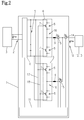
- Fig. 2 shows a possible embodiment of an inverter 1, in which the individual semiconductor switches 7, including the parallel-connected freewheeling diodes 8 of the AC power parts 6 are visible.
- the semiconductor switches 7 are driven by the control device 11 at the switching frequency f S.
- the AC power parts 6 to 2-point half-bridges 16, which are connected in parallel via inductors 9.
- one of the two semiconductor switches 7 of a half bridge 16 is usually always conductive, so that the alternating voltage output 10 is connected either to the positive or negative DC link potential.
- another bridge circuit topology such as a 3-point half-bridge, conceivable.
- the alternating output current I AC is not uniformly divided between the parallel AC power parts 6 due to flux voltage differences, the transmission characteristics and / or different dynamic switching behavior of the AC power parts 6 or their semiconductor switches 7. Rather, during operation, the partial output currents I A1 , I A2 of the individual AC power parts 6 may drift apart from one another.
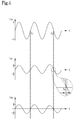
- Fig. 3 shows a corresponding example of the output AC current I AC and the partial output currents I A1 , I A2 at two parallel AC power parts 6. In this case corresponds to the period T AC the reciprocal of the predetermined mains frequency f AC .
- the partial output current I A1 of the first AC power unit 6 increases by a continuously increasing DC component while the partial output current I A2 of the second AC power unit 6 decreases by the same DC component.
- the sum of the partial output currents I A1 , I A2 of the AC power parts 6 result in the amplitude and frequency constant output AC current I AC , in FIG. 3 is shown in the upper diagram.
- the semiconductor switch 7 of the AC power parts 6 are simultaneously disabled at individual zero crossings of the AC output current I AC over a predetermined period of time t F to achieve a symmetrical current distribution of the AC output current I AC or to reduce the asymmetry in the distribution.
- the inductors 9 are discharged via the freewheeling diodes 8 of the semiconductor switches 7 and thereby the partial output currents I A1 , I A2 of the parallel AC power parts 6 are balanced.
- This symmetry takes place after two half waves at time t 1 and after three further half waves at time t 2 .
- the partial output current I A1 of the first AC power unit 6 is shown at the time t 2 .
- the symmetrically split AC output AC in this example, half the AC output AC I, dashed lines drawn. This actually corresponds to the desired partial output current I A1 of the AC power unit 6.
- the output currents I A1 , I A2 Due to asymmetries in the electronic components and the switching behavior of the semiconductor switches 7, the output currents I A1 , I A2 have a deviation from the desired course, with this deviation usually builds up over several half-waves. Therefore, the semiconductor switches 7 are blocked for the time t F before the zero crossing of the AC output current I AC of the control device 11 at the same time.
- the supply output currents I A1, I A2 may, depending on their current level via the freewheeling diodes 8 but decay to zero in any case the portion of output currents I A1, I A2, and thus the Unsymmtrie the current distribution can be reduced.
- the semiconductor switches 7 are driven again. The required after the zero crossing output AC current I AC is now, since both AC power parts 6 were previously de-energized, symmetrically split over the half-bridges 16 of the AC power parts 6 to the AC output 10 of the inverter 1 passed.
- a particularly simple design of the inverter 11 is achieved by the semiconductor switches 7 of the parallel-connected AC power parts 6 are controlled synchronously by the common control device 11.
- the functionally identical semiconductor switches 7, as in Fig. 2 represented, via common lines 17, 18 are driven, but also the control with separate control lines, which have the same signals is conceivable.
- the time interval between the applications of the method can be varied, ie that the method does not have to be performed after each half cycle or after each period. Rather, it has been found that when using the method after every nth zero crossing of the output alternating current I AC , where n is an odd integer number, in particular a prime number is less than 500, caused by the blocking of the semiconductor switch 7 disturbances in the frequency spectrum of the AC output current I AC kept small. Especially when using an odd interval of zero crossings for the application of the method, on average, the effects of interruption of the AC output current I AC at positive and negative half-wave cancel and it can be a DC offset can be avoided.
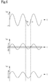
- Fig. 5 shows how the interval for the application of the method is varied depending on the size of the AC output current AC .
- the symmetry method is applied every fifth half-wave at the times t S
- the method is applied every third half-cycle at the times t S is applied.
- the frequency of application of the method is thus adapted to the respective requirements.
- the partial output currents I A1 , I A2 of each AC power section 6 and the AC output current I AC can be detected by means of sensors 14, 15 or similar devices for current measurement, such as current transformers.
- sensors 14, 15 or similar devices for current measurement such as current transformers.
- a sensor 14 for measuring the AC output current I AC and a respective sensor 15 for measuring the partial output currents I A1 , I A2 arranged. Due to the node rule of the first Kirchhoff's law it is not necessary to supply output currents I A1, I A2 to capture every AC power unit 6 and the output AC current I AC, as one of the currents I A1, I A2 or I AC in Measurement of all remaining currents, can also calculate.
- the maximum height of the individual partial output currents I A1 , I A2 of the parallel AC power parts 6 at the time of the zero crossing of the output alternating current I AC is a measure of the current asymmetry, whereby the actual presence of an imbalance is detected. Accordingly, the method is performed only when a defined partial output current I A1 , I A2 of one of the parallel AC power parts 6 at the zero crossing of the AC output current I AC and the semiconductor switches 7 of the parallel AC power parts 6 over the predetermined period t F locked.
- Fig. 6 shows the partial output currents I A1 , I A2 of the parallel AC power parts 6 and the defined as the threshold value I S partial output current I A1 , I A2 , when exceeded, the inventive method is performed.
- the threshold value I S represents an amount and the method is carried out both in the case of a positive overshoot and a negative undershoot. Since the current imbalance in the zero crossing of the AC output current I AC at the time t M is detected, the method for balancing the partial output currents I A1 , I A2 as in Fig. 6 shown before the next zero crossing of the AC output current I AC performed at time t S. A variant not shown in detail, in which the method is performed directly after the zero crossing of the AC output current AC at the time t M , would also be applicable.
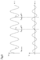
- Fig. 7 shows by way of example how the predetermined time period t F is selected depending on the largest partial output current I A1 , I A2 of the parallel AC power parts 6 at the zero crossing of the AC output current AC . Simplifying only one of the partial output current I A1 is shown. In this embodiment, the current balancing is performed every 3rd half-wave. Depending on the size of the partial output current I A1 at the zero crossing of the output AC current I AC , the predetermined time period t F is selected such that the partial output current I A1 decays to zero within the predetermined time period t F. Accordingly, t F1 is greater than t F3, which in turn is greater than t F2 .
- the duration of application of the method can thus be shortened to the minimum necessary time, as a result of which disturbances in the signal curve of the AC voltage U AC at the AC output 10 of the inverter 1 are reduced.
- the assessment of the size of the partial output currents I A1 , I A2 at the zero crossing of the AC output AC I take a half-wave before the actual balancing or the current waveform of the partial output currents I A1 , I A2 is precalculated, as shown by the dashed lines of the current waveform of the partial output current I A1 in Fig. 7 indicated.
- FIG. 12 shows another exemplary application of the method in which the number of zero crossings between the applications of the method is also varied. Besides, it is off Fig. 8 the application of the method immediately after the zero crossing apparent. Furthermore, a stochastic variation of the predetermined time period t F is used here. Thus, at time t 1, the method is applied for the predetermined period of time t F. By contrast, at the times t 2 and t 3 , the predetermined time period t F is increased by ⁇ t F2 or ⁇ t F3 . At time t 2 can be recognized also that a decay of the supply output current I A1 to zero is not absolutely necessary because even a partial decay of the supply output current I A1 provides an improvement in the current balancing with it.
- This stochastic variation of the time period t F can contribute to the reduction of disturbances in the signal path of the AC voltage U AC at the AC output 10 of the inverter 1.
- the method is particularly simple to implement by selecting the predetermined time period t F as a period of the switching frequency f S.
Landscapes
- Engineering & Computer Science (AREA)
- Power Engineering (AREA)
- Inverter Devices (AREA)
Priority Applications (9)
| Application Number | Priority Date | Filing Date | Title |
|---|---|---|---|
| EP16191753.9A EP3301805A1 (fr) | 2016-09-30 | 2016-09-30 | Procédé destiné au fonctionnement d'un onduleur et onduleur |
| BR112019004008-0A BR112019004008B1 (pt) | 2016-09-30 | 2017-09-29 | Método para operação de um inversor, e inversor |
| AU2017336307A AU2017336307B2 (en) | 2016-09-30 | 2017-09-29 | Method for operating an inverter, and inverter |
| PL17783785T PL3520213T3 (pl) | 2016-09-30 | 2017-09-29 | Sposób działania falownika oraz falownik |
| EP17783785.3A EP3520213B1 (fr) | 2016-09-30 | 2017-09-29 | Procédé destiné au fonctionnement d'un onduleur et onduleur |
| PCT/EP2017/074760 WO2018060414A1 (fr) | 2016-09-30 | 2017-09-29 | Procédé de fonctionnement d'un onduleur et onduleur |
| CN201780059991.2A CN109874388B (zh) | 2016-09-30 | 2017-09-29 | 用于操作逆变器的方法及逆变器 |
| US16/337,547 US10811996B2 (en) | 2016-09-30 | 2017-09-29 | Method for operating an inverter, and inverter |
| IL265651A IL265651B (en) | 2016-09-30 | 2019-03-26 | Method for operating an inverter, and inverter |
Applications Claiming Priority (1)
| Application Number | Priority Date | Filing Date | Title |
|---|---|---|---|
| EP16191753.9A EP3301805A1 (fr) | 2016-09-30 | 2016-09-30 | Procédé destiné au fonctionnement d'un onduleur et onduleur |
Publications (1)
| Publication Number | Publication Date |
|---|---|
| EP3301805A1 true EP3301805A1 (fr) | 2018-04-04 |
Family
ID=57042824
Family Applications (2)
| Application Number | Title | Priority Date | Filing Date |
|---|---|---|---|
| EP16191753.9A Withdrawn EP3301805A1 (fr) | 2016-09-30 | 2016-09-30 | Procédé destiné au fonctionnement d'un onduleur et onduleur |
| EP17783785.3A Active EP3520213B1 (fr) | 2016-09-30 | 2017-09-29 | Procédé destiné au fonctionnement d'un onduleur et onduleur |
Family Applications After (1)
| Application Number | Title | Priority Date | Filing Date |
|---|---|---|---|
| EP17783785.3A Active EP3520213B1 (fr) | 2016-09-30 | 2017-09-29 | Procédé destiné au fonctionnement d'un onduleur et onduleur |
Country Status (7)
| Country | Link |
|---|---|
| US (1) | US10811996B2 (fr) |
| EP (2) | EP3301805A1 (fr) |
| CN (1) | CN109874388B (fr) |
| AU (1) | AU2017336307B2 (fr) |
| IL (1) | IL265651B (fr) |
| PL (1) | PL3520213T3 (fr) |
| WO (1) | WO2018060414A1 (fr) |
Families Citing this family (2)
| Publication number | Priority date | Publication date | Assignee | Title |
|---|---|---|---|---|
| AT523580B1 (de) * | 2020-03-05 | 2023-12-15 | Avl List Gmbh | Umrichteranordnung und Verfahren zum Betrieb einer Umrichteranordnung |
| EP4482005A1 (fr) * | 2023-06-21 | 2024-12-25 | Abb Schweiz Ag | Agencement pour le partage de courant de convertisseurs connectés en parallèle |
Citations (3)
| Publication number | Priority date | Publication date | Assignee | Title |
|---|---|---|---|---|
| WO2009003959A2 (fr) | 2007-06-29 | 2009-01-08 | Enasys Gmbh | Système d'onduleurs et procédé de commande |
| DE102007046511A1 (de) * | 2007-09-28 | 2009-04-23 | Siemens Ag | Stromrichter mit unterbrechbarem Parallelkreis und Umrichter mit zwei parallelkreis-unterbrechenden Stromrichtern |
| EP2887519A2 (fr) * | 2013-12-18 | 2015-06-24 | Thales | Dispositif de conversion de puissance électrique modulaire et reconfigurable |
Family Cites Families (11)
| Publication number | Priority date | Publication date | Assignee | Title |
|---|---|---|---|---|
| US5574636A (en) * | 1994-09-09 | 1996-11-12 | Center For Innovative Technology | Zero-voltage-transition (ZVT) 3-phase PWM voltage link converters |
| US20050180175A1 (en) * | 2004-02-12 | 2005-08-18 | Torrey David A. | Inverter topology for utility-interactive distributed generation sources |
| CN101388612B (zh) * | 2007-09-14 | 2011-08-31 | 力博特公司 | 一种开关电源中软开关电路的控制方法 |
| JP5205973B2 (ja) * | 2008-01-08 | 2013-06-05 | 日本精工株式会社 | 電動パワーステアリング装置の制御装置 |
| JP5230777B2 (ja) * | 2011-07-06 | 2013-07-10 | 三菱電機株式会社 | 電力変換装置 |
| CN103795251A (zh) * | 2012-10-29 | 2014-05-14 | 台达电子工业股份有限公司 | 功率变换器及其控制方法 |
| US9641099B2 (en) * | 2013-03-15 | 2017-05-02 | Sparq Systems Inc. | DC-AC inverter with soft switching |
| JP5679239B1 (ja) * | 2013-08-27 | 2015-03-04 | 株式会社京三製作所 | 単相インバータ |
| DE102014102000B3 (de) * | 2014-02-18 | 2014-09-11 | Sma Solar Technology Ag | Verfahren zum Betreiben eines blindleistungsfähigen Wechselrichters mit Polwender und blindleistungsfähiger Wechselrichter mit Polwender |
| US9853591B2 (en) | 2014-03-31 | 2017-12-26 | Aisin Aw Co., Ltd. | Inverter control device |
| WO2017025490A1 (fr) * | 2015-08-07 | 2017-02-16 | Sma Solar Technology Ag | Onduleur inverseur de polarité et avec capacité de puissance réactive ainsi que procédé d'inversion de polarité |
-
2016
- 2016-09-30 EP EP16191753.9A patent/EP3301805A1/fr not_active Withdrawn
-
2017
- 2017-09-29 EP EP17783785.3A patent/EP3520213B1/fr active Active
- 2017-09-29 WO PCT/EP2017/074760 patent/WO2018060414A1/fr not_active Ceased
- 2017-09-29 AU AU2017336307A patent/AU2017336307B2/en active Active
- 2017-09-29 PL PL17783785T patent/PL3520213T3/pl unknown
- 2017-09-29 CN CN201780059991.2A patent/CN109874388B/zh active Active
- 2017-09-29 US US16/337,547 patent/US10811996B2/en active Active
-
2019
- 2019-03-26 IL IL265651A patent/IL265651B/en active IP Right Grant
Patent Citations (3)
| Publication number | Priority date | Publication date | Assignee | Title |
|---|---|---|---|---|
| WO2009003959A2 (fr) | 2007-06-29 | 2009-01-08 | Enasys Gmbh | Système d'onduleurs et procédé de commande |
| DE102007046511A1 (de) * | 2007-09-28 | 2009-04-23 | Siemens Ag | Stromrichter mit unterbrechbarem Parallelkreis und Umrichter mit zwei parallelkreis-unterbrechenden Stromrichtern |
| EP2887519A2 (fr) * | 2013-12-18 | 2015-06-24 | Thales | Dispositif de conversion de puissance électrique modulaire et reconfigurable |
Also Published As
| Publication number | Publication date |
|---|---|
| PL3520213T3 (pl) | 2020-08-10 |
| CN109874388A (zh) | 2019-06-11 |
| IL265651A (en) | 2019-05-30 |
| CN109874388B (zh) | 2020-01-14 |
| AU2017336307B2 (en) | 2022-04-07 |
| US20200036298A1 (en) | 2020-01-30 |
| EP3520213B1 (fr) | 2020-04-01 |
| WO2018060414A1 (fr) | 2018-04-05 |
| US10811996B2 (en) | 2020-10-20 |
| IL265651B (en) | 2019-09-26 |
| AU2017336307A1 (en) | 2019-04-04 |
| BR112019004008A2 (pt) | 2019-06-04 |
| EP3520213A1 (fr) | 2019-08-07 |
Similar Documents
| Publication | Publication Date | Title |
|---|---|---|
| DE69506612T2 (de) | Steuerschaltung für induktive Belastung | |
| DE4206263C2 (de) | Steuersatz für pulsbreitenmodulierten Dreipunktwechselrichter | |
| EP3245727B1 (fr) | Module convertisseur pour convertisseur d'énergie multiniveaux | |
| EP1759450B1 (fr) | Circuit commutateur polyphase pauvre en oscillations harmoniques | |
| EP4046268B1 (fr) | Détermination des paramètres de filtrage dans un onduleur | |
| DE102014105289A1 (de) | Aktiver EMV Filter | |
| DE102013212426A1 (de) | Umrichteranordnung mit parallel geschalteten Mehrstufen-Umrichtern sowie Verfahren zu deren Steuerung | |
| DE3525413A1 (de) | Elektromagnetischer stroemungsmesser | |
| EP3520213B1 (fr) | Procédé destiné au fonctionnement d'un onduleur et onduleur | |
| WO2013023914A1 (fr) | Dispositif onduleur | |
| EP2182626B1 (fr) | Procédé destiné au fonctionnement d'un convertisseur de courant et convertisseur de courant fonctionnant selon ce procédé | |
| DE102013212048A1 (de) | Z-Source-Inverter mit optimiertem Wirkungsgrad | |
| DE102017005928A1 (de) | Umrichtersystem und Verfahren zum Betreiben eines Umrichtersystems | |
| EP0502226A1 (fr) | Procédé et dispositif pour simuler les courants dans une machine à champ tournant alimentée par onduleur | |
| EP2966769A1 (fr) | Fonctionnement d'un convertisseur multi-étagé modulaire | |
| EP0865138A1 (fr) | Procédé et dispositif pour la formation d'une tension alternative | |
| DE4406371B4 (de) | Verfahren zur Helligkeitssteuerung für Glühlampen und Schaltnetzteile | |
| EP3714539B1 (fr) | Convertisseur stable en court-circuit à commande de courant directe | |
| DE3437242A1 (de) | Elektronischer leistungssteller, insbesondere zur regelung der auslauftemperatur bei elektrischen durchlauferhitzern | |
| EP3806314A1 (fr) | Onduleur pour un réseau de courant alternatif | |
| CH708040A2 (de) | Elektronischer Leistungswandler und Verfahren zu dessen Ansteuerung. | |
| DE112014007091T5 (de) | Hilfsstromversorgungseinrichtung für ein elektrisches Triebfahrzeug | |
| EP3089340B1 (fr) | Élement d'un reseau de distribution destine a alimenter un convertisseur | |
| DE4019665C1 (fr) | ||
| EP2928056B1 (fr) | Procédé et dispositif de fonctionnement d'un convertisseur de courant modulaire avec une grande vitesse de commutation ajustable |
Legal Events
| Date | Code | Title | Description |
|---|---|---|---|
| PUAI | Public reference made under article 153(3) epc to a published international application that has entered the european phase |
Free format text: ORIGINAL CODE: 0009012 |
|
| STAA | Information on the status of an ep patent application or granted ep patent |
Free format text: STATUS: THE APPLICATION HAS BEEN PUBLISHED |
|
| AK | Designated contracting states |
Kind code of ref document: A1 Designated state(s): AL AT BE BG CH CY CZ DE DK EE ES FI FR GB GR HR HU IE IS IT LI LT LU LV MC MK MT NL NO PL PT RO RS SE SI SK SM TR |
|
| AX | Request for extension of the european patent |
Extension state: BA ME |
|
| STAA | Information on the status of an ep patent application or granted ep patent |
Free format text: STATUS: THE APPLICATION IS DEEMED TO BE WITHDRAWN |
|
| 18D | Application deemed to be withdrawn |
Effective date: 20181005 |