EP3312899B1 - Elektronentransportschichtstapel für eine organische lichtemittierende diode - Google Patents
Elektronentransportschichtstapel für eine organische lichtemittierende diode Download PDFInfo
- Publication number
- EP3312899B1 EP3312899B1 EP16195344.3A EP16195344A EP3312899B1 EP 3312899 B1 EP3312899 B1 EP 3312899B1 EP 16195344 A EP16195344 A EP 16195344A EP 3312899 B1 EP3312899 B1 EP 3312899B1
- Authority
- EP
- European Patent Office
- Prior art keywords
- group
- substituted
- unsubstituted
- electron transport
- transport layer
- Prior art date
- Legal status (The legal status is an assumption and is not a legal conclusion. Google has not performed a legal analysis and makes no representation as to the accuracy of the status listed.)
- Active
Links
- 0 CC(*)CC(C)([C@@]([C@@](C)CNCC1C=C(*)C*C1)C=CIC(C)C(C)[C@]1[C@](C)C1)S Chemical compound CC(*)CC(C)([C@@]([C@@](C)CNCC1C=C(*)C*C1)C=CIC(C)C(C)[C@]1[C@](C)C1)S 0.000 description 4
- LCLULYKHEHNZBI-UHFFFAOYSA-N [I-]c1c(ccc2ccccc22)c2nc2c1ccc1ccccc21 Chemical compound [I-]c1c(ccc2ccccc22)c2nc2c1ccc1ccccc21 LCLULYKHEHNZBI-UHFFFAOYSA-N 0.000 description 1
- CGMVNBNIECPAFE-UHFFFAOYSA-N [I-]c1c(ccc2ccccc22)c2nc2ccccc12 Chemical compound [I-]c1c(ccc2ccccc22)c2nc2ccccc12 CGMVNBNIECPAFE-UHFFFAOYSA-N 0.000 description 1
- XQQKCSNLLGHJQH-UHFFFAOYSA-N c(cc1)cc(cc2)c1c1c2c(-c2cc(-c3cc(-c4cnccc4)cc(-c4cnccc4)c3)ccc2)c(ccc2ccccc22)c2n1 Chemical compound c(cc1)cc(cc2)c1c1c2c(-c2cc(-c3cc(-c4cnccc4)cc(-c4cnccc4)c3)ccc2)c(ccc2ccccc22)c2n1 XQQKCSNLLGHJQH-UHFFFAOYSA-N 0.000 description 1
- KRGZCOASGYWGOT-UHFFFAOYSA-N c(cc1)cc(cc2)c1c1c2c(-c2cc(-c3ccncc3)ccc2)c(ccc2ccccc22)c2n1 Chemical compound c(cc1)cc(cc2)c1c1c2c(-c2cc(-c3ccncc3)ccc2)c(ccc2ccccc22)c2n1 KRGZCOASGYWGOT-UHFFFAOYSA-N 0.000 description 1
- JIYIQUYALSYZSK-UHFFFAOYSA-N c(cc1cc2)ccc1c1c2c(-c2cccc(-c3cccc(-c4cccc5c4nccc5)c3)c2)c(ccc2ccccc22)c2n1 Chemical compound c(cc1cc2)ccc1c1c2c(-c2cccc(-c3cccc(-c4cccc5c4nccc5)c3)c2)c(ccc2ccccc22)c2n1 JIYIQUYALSYZSK-UHFFFAOYSA-N 0.000 description 1
Images
Classifications
-
- C—CHEMISTRY; METALLURGY
- C07—ORGANIC CHEMISTRY
- C07D—HETEROCYCLIC COMPOUNDS
- C07D221/00—Heterocyclic compounds containing six-membered rings having one nitrogen atom as the only ring hetero atom, not provided for by groups C07D211/00 - C07D219/00
- C07D221/02—Heterocyclic compounds containing six-membered rings having one nitrogen atom as the only ring hetero atom, not provided for by groups C07D211/00 - C07D219/00 condensed with carbocyclic rings or ring systems
- C07D221/04—Ortho- or peri-condensed ring systems
- C07D221/18—Ring systems of four or more rings
-
- H—ELECTRICITY
- H10—SEMICONDUCTOR DEVICES; ELECTRIC SOLID-STATE DEVICES NOT OTHERWISE PROVIDED FOR
- H10K—ORGANIC ELECTRIC SOLID-STATE DEVICES
- H10K50/00—Organic light-emitting devices
- H10K50/10—OLEDs or polymer light-emitting diodes [PLED]
- H10K50/14—Carrier transporting layers
- H10K50/16—Electron transporting layers
- H10K50/166—Electron transporting layers comprising a multilayered structure
-
- C—CHEMISTRY; METALLURGY
- C07—ORGANIC CHEMISTRY
- C07D—HETEROCYCLIC COMPOUNDS
- C07D251/00—Heterocyclic compounds containing 1,3,5-triazine rings
- C07D251/02—Heterocyclic compounds containing 1,3,5-triazine rings not condensed with other rings
- C07D251/12—Heterocyclic compounds containing 1,3,5-triazine rings not condensed with other rings having three double bonds between ring members or between ring members and non-ring members
- C07D251/14—Heterocyclic compounds containing 1,3,5-triazine rings not condensed with other rings having three double bonds between ring members or between ring members and non-ring members with hydrogen or carbon atoms directly attached to at least one ring carbon atom
- C07D251/24—Heterocyclic compounds containing 1,3,5-triazine rings not condensed with other rings having three double bonds between ring members or between ring members and non-ring members with hydrogen or carbon atoms directly attached to at least one ring carbon atom to three ring carbon atoms
-
- C—CHEMISTRY; METALLURGY
- C07—ORGANIC CHEMISTRY
- C07D—HETEROCYCLIC COMPOUNDS
- C07D401/00—Heterocyclic compounds containing two or more hetero rings, having nitrogen atoms as the only ring hetero atoms, at least one ring being a six-membered ring with only one nitrogen atom
- C07D401/02—Heterocyclic compounds containing two or more hetero rings, having nitrogen atoms as the only ring hetero atoms, at least one ring being a six-membered ring with only one nitrogen atom containing two hetero rings
- C07D401/10—Heterocyclic compounds containing two or more hetero rings, having nitrogen atoms as the only ring hetero atoms, at least one ring being a six-membered ring with only one nitrogen atom containing two hetero rings linked by a carbon chain containing aromatic rings
-
- C—CHEMISTRY; METALLURGY
- C07—ORGANIC CHEMISTRY
- C07D—HETEROCYCLIC COMPOUNDS
- C07D495/00—Heterocyclic compounds containing in the condensed system at least one hetero ring having sulfur atoms as the only ring hetero atoms
- C07D495/02—Heterocyclic compounds containing in the condensed system at least one hetero ring having sulfur atoms as the only ring hetero atoms in which the condensed system contains two hetero rings
- C07D495/04—Ortho-condensed systems
-
- H—ELECTRICITY
- H10—SEMICONDUCTOR DEVICES; ELECTRIC SOLID-STATE DEVICES NOT OTHERWISE PROVIDED FOR
- H10K—ORGANIC ELECTRIC SOLID-STATE DEVICES
- H10K50/00—Organic light-emitting devices
- H10K50/10—OLEDs or polymer light-emitting diodes [PLED]
- H10K50/11—OLEDs or polymer light-emitting diodes [PLED] characterised by the electroluminescent [EL] layers
- H10K50/12—OLEDs or polymer light-emitting diodes [PLED] characterised by the electroluminescent [EL] layers comprising dopants
-
- H—ELECTRICITY
- H10—SEMICONDUCTOR DEVICES; ELECTRIC SOLID-STATE DEVICES NOT OTHERWISE PROVIDED FOR
- H10K—ORGANIC ELECTRIC SOLID-STATE DEVICES
- H10K50/00—Organic light-emitting devices
- H10K50/10—OLEDs or polymer light-emitting diodes [PLED]
- H10K50/14—Carrier transporting layers
- H10K50/15—Hole transporting layers
-
- H—ELECTRICITY
- H10—SEMICONDUCTOR DEVICES; ELECTRIC SOLID-STATE DEVICES NOT OTHERWISE PROVIDED FOR
- H10K—ORGANIC ELECTRIC SOLID-STATE DEVICES
- H10K50/00—Organic light-emitting devices
- H10K50/10—OLEDs or polymer light-emitting diodes [PLED]
- H10K50/17—Carrier injection layers
-
- H—ELECTRICITY
- H10—SEMICONDUCTOR DEVICES; ELECTRIC SOLID-STATE DEVICES NOT OTHERWISE PROVIDED FOR
- H10K—ORGANIC ELECTRIC SOLID-STATE DEVICES
- H10K50/00—Organic light-emitting devices
- H10K50/10—OLEDs or polymer light-emitting diodes [PLED]
- H10K50/18—Carrier blocking layers
-
- H—ELECTRICITY
- H10—SEMICONDUCTOR DEVICES; ELECTRIC SOLID-STATE DEVICES NOT OTHERWISE PROVIDED FOR
- H10K—ORGANIC ELECTRIC SOLID-STATE DEVICES
- H10K59/00—Integrated devices, or assemblies of multiple devices, comprising at least one organic light-emitting element covered by group H10K50/00
-
- H—ELECTRICITY
- H10—SEMICONDUCTOR DEVICES; ELECTRIC SOLID-STATE DEVICES NOT OTHERWISE PROVIDED FOR
- H10K—ORGANIC ELECTRIC SOLID-STATE DEVICES
- H10K85/00—Organic materials used in the body or electrodes of devices covered by this subclass
- H10K85/60—Organic compounds having low molecular weight
- H10K85/615—Polycyclic condensed aromatic hydrocarbons, e.g. anthracene
- H10K85/622—Polycyclic condensed aromatic hydrocarbons, e.g. anthracene containing four rings, e.g. pyrene
-
- H—ELECTRICITY
- H10—SEMICONDUCTOR DEVICES; ELECTRIC SOLID-STATE DEVICES NOT OTHERWISE PROVIDED FOR
- H10K—ORGANIC ELECTRIC SOLID-STATE DEVICES
- H10K85/00—Organic materials used in the body or electrodes of devices covered by this subclass
- H10K85/60—Organic compounds having low molecular weight
- H10K85/649—Aromatic compounds comprising a hetero atom
- H10K85/654—Aromatic compounds comprising a hetero atom comprising only nitrogen as heteroatom
-
- H—ELECTRICITY
- H10—SEMICONDUCTOR DEVICES; ELECTRIC SOLID-STATE DEVICES NOT OTHERWISE PROVIDED FOR
- H10K—ORGANIC ELECTRIC SOLID-STATE DEVICES
- H10K85/00—Organic materials used in the body or electrodes of devices covered by this subclass
- H10K85/60—Organic compounds having low molecular weight
- H10K85/649—Aromatic compounds comprising a hetero atom
- H10K85/657—Polycyclic condensed heteroaromatic hydrocarbons
- H10K85/6572—Polycyclic condensed heteroaromatic hydrocarbons comprising only nitrogen in the heteroaromatic polycondensed ring system, e.g. phenanthroline or carbazole
-
- H—ELECTRICITY
- H10—SEMICONDUCTOR DEVICES; ELECTRIC SOLID-STATE DEVICES NOT OTHERWISE PROVIDED FOR
- H10K—ORGANIC ELECTRIC SOLID-STATE DEVICES
- H10K2101/00—Properties of the organic materials covered by group H10K85/00
- H10K2101/10—Triplet emission
-
- H—ELECTRICITY
- H10—SEMICONDUCTOR DEVICES; ELECTRIC SOLID-STATE DEVICES NOT OTHERWISE PROVIDED FOR
- H10K—ORGANIC ELECTRIC SOLID-STATE DEVICES
- H10K50/00—Organic light-emitting devices
- H10K50/10—OLEDs or polymer light-emitting diodes [PLED]
- H10K50/11—OLEDs or polymer light-emitting diodes [PLED] characterised by the electroluminescent [EL] layers
-
- H—ELECTRICITY
- H10—SEMICONDUCTOR DEVICES; ELECTRIC SOLID-STATE DEVICES NOT OTHERWISE PROVIDED FOR
- H10K—ORGANIC ELECTRIC SOLID-STATE DEVICES
- H10K50/00—Organic light-emitting devices
- H10K50/10—OLEDs or polymer light-emitting diodes [PLED]
- H10K50/14—Carrier transporting layers
- H10K50/16—Electron transporting layers
- H10K50/165—Electron transporting layers comprising dopants
-
- H—ELECTRICITY
- H10—SEMICONDUCTOR DEVICES; ELECTRIC SOLID-STATE DEVICES NOT OTHERWISE PROVIDED FOR
- H10K—ORGANIC ELECTRIC SOLID-STATE DEVICES
- H10K59/00—Integrated devices, or assemblies of multiple devices, comprising at least one organic light-emitting element covered by group H10K50/00
- H10K59/10—OLED displays
-
- H—ELECTRICITY
- H10—SEMICONDUCTOR DEVICES; ELECTRIC SOLID-STATE DEVICES NOT OTHERWISE PROVIDED FOR
- H10K—ORGANIC ELECTRIC SOLID-STATE DEVICES
- H10K71/00—Manufacture or treatment specially adapted for the organic devices covered by this subclass
-
- H—ELECTRICITY
- H10—SEMICONDUCTOR DEVICES; ELECTRIC SOLID-STATE DEVICES NOT OTHERWISE PROVIDED FOR
- H10K—ORGANIC ELECTRIC SOLID-STATE DEVICES
- H10K71/00—Manufacture or treatment specially adapted for the organic devices covered by this subclass
- H10K71/40—Thermal treatment, e.g. annealing in the presence of a solvent vapour
-
- H—ELECTRICITY
- H10—SEMICONDUCTOR DEVICES; ELECTRIC SOLID-STATE DEVICES NOT OTHERWISE PROVIDED FOR
- H10K—ORGANIC ELECTRIC SOLID-STATE DEVICES
- H10K85/00—Organic materials used in the body or electrodes of devices covered by this subclass
- H10K85/30—Coordination compounds
Definitions
- OLEDs Organic light-emitting diodes
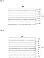
- a typical OLED includes an anode, a hole transport layer HTL, an emission layer EML , an electron transport layer ETL , and a cathode, which are sequentially stacked on a substrate.
- the HTL, the EML, and the ETL are thin films formed from organic compounds.
- WO2011154131A1 relates to an electronic device comprising at least one organic semiconducting material according to the following formula (A): wherein R1-4 are independently selected from H, halogen, CN, substituted or unsubstituted C1- C20-alkyl or heteroalkyl, C6-C20-aryl or C5-C20-heteroaryl, C1-C20-alkoxy or C6-C20-aryloxy, Ar is selected from substituted or unsubstituted C6-C20-aryl or C5-C20-heteroaryl, and R5 is selected from substituted or unsubstituted C6-C20-aryl or C5-C20-heteroaryl, H, F or formula (B).
- R1-4 are independently selected from H, halogen, CN, substituted or unsubstituted C1- C20-alkyl or heteroalkyl, C6-C20-aryl or C5-C20-heteroaryl
- US2006057427 discloses an OLED comprising two electron transport layers, wherein one of the electron transport layers contains a compound according to Chemical Formula I.
- US2015034915 relates to an OLED having an electron transport layer composed of a benzoacridine derivative doped with a lithium complex.
- OLED organic light-emitting diode
- ETLs electron transport layers
- the alkali metal salt or alkali metal organic complex contained in the electron transport layers may not emit light under the operation condition of an electroluminescent device, for example an OLED.
- substituted refers to one substituted with a deuterium, C 1 to C 12 alkyl and C 1 to C 12 alkoxy.
- cycloalkyl refers to saturated hydrocarbyl groups derived from a cycloalkane by formal abstraction of one hydrogen atom from a ring atom comprised in the corresponding cycloalkane.
- examples of the cycloalkyl group may be a cyclopropyl group, a cyclobutyl group, a cyclopentyl group, a cyclohexyl group, a methylcyclohexyl group, an adamantly group and the like.
- heterocycloalkyl it is understood a group derived by formal abstraction of one ring hydrogen from a saturated heterocyclic ring in a compound comprising at least one such ring.
- heteroaryl refers to aryl groups in which at least one carbon atom is substituted by a heteroatom, preferably selected from N, O, S, B or Si.
- Heteroarylene refers to groups to which two further moieties are attached.
- C n in C n -heteroaryl merely refers to the number of carbon atoms excluding the number of heteroatoms.
- a C 5 heteroarylene group is an aromatic compound comprising five carbon atoms, such as pyridyl.
- the single bond may refer to a direct bond.
- contacting sandwiched refers to an arrangement of three layers whereby the layer in the middle is in direct contact with the two adjacent layers.
- electron characteristics refer to an ability to accept an electron when an electric field is applied and that electron formed in the cathode may be easily injected into the emission layer and transported in the emission layer due to conductive characteristics according to a lowest unoccupied molecular orbital (LUMO) level.
- LUMO lowest unoccupied molecular orbital
- an ETL layer stack of the invention solves the problem underlying the present invention by being superior over the organic electroluminescent devices known in the art, in particular with respect cd/A efficiency.
- High cd/A efficiency is important for high efficiency and thereby increased battery life of a mobile device, for example a mobile display device.
- organic electroluminescent device having high efficiency and/or long life-span may be realized.
- the first electron transport layer comprises a first electron matrix compound according to formula (Ia): wherein, in formula Ia
- One or more substituents may be selected from C 4 to C 12 alkyl or C 4 to C 12 alkoxy. Particularly good properties in solution processed layers may be obtained, when the compound of formula I is selected in this range.
- the ET group is a C 2 to C 30 heteroaryl group, preferably ET is selected from formula E1 or E2: wherein Ar' and Ar" are independently selected from C 6 to C 18 aryl, preferably from C 6 to C 12 aryl.
- ET is selected from formula E1.
- the compound of formula I is essentially non-emissive.
- triphenylphosphine oxide is about -3.06 V and the reduction potential of tetrakis(quinoxalin-5-yloxy)zirconium is about -1.78 V.
- the first run was done in the broadest range of the potential set on the working electrodes, and the range was then adjusted within subsequent runs appropriately.
- the final three runs were done with the addition of ferrocene (in 0.1M concentration) as the standard.
- ferrocene in 0.1M concentration
- the compound of formula I may have a glass transition temperature (Tg) selected between ⁇ 125° C and ⁇ 200° C, preferably ⁇ 130° C and ⁇ 180° C.
- Tg glass transition temperature
- Lithium organic complex that can be suitable used Compound Name Structure Disclosed in: LiQ lithium 8-hydroxyquinolate WO 2013079217 A1 Li-1 lithium tetra(1 H-pyrazol-1 - yl)borate WO 2013079676 A1 Li-2 lithium 2-(diphenylphosphoryl)phenolate WO 2013079678A1 Li-3 lithium 2-(pyridin-2-yl)phenolate JP2 008195623 Li-4 lithium 2-(1 -phenyl-1 H-benzo [d]imidazol-2-yl)phenolate JP 2001291593 Li-5 lithium 2-(benzo[d]oxazol-2-yl)phenolate US 20030165711 Li-6 lithium 2-(diphenylphosphoryl)pyridin-3-olate EP 2724388
- the alkali metal salt and alkali metal organic complex may be essentially non-emissive.
- the first electron transport layer can be in direct contact with the second electron transport layer.
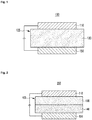
- the hole injection layer 37 may improve interface properties between ITO as an anode and an organic material used for the hole transport layer 31, and is applied on a non-planarized ITO and thus planarizes the surface of the ITO.
- the hole injection layer 37 may include a material having a median value, particularly desirable conductivity between a work function of ITO and HOMO of the hole transport layer 31, in order to adjust a difference a work function of ITO as an anode and HOMO of the hole transport layer 31.
- the hole injection layer may be formed on the anode 150 by any of a variety of methods, for example, vacuum deposition, spin coating, casting, Langmuir-Blodgett (LB) method, or the like.
- the coating conditions may vary depending on the material that is used to form the hole injection layer, and the desired structure and thermal properties of the hole injection layer to be formed.
- the coating rate may be in the range of about 2000 rpm to about 5000 rpm
- a temperature at which heat treatment is performed to remove a solvent after coating may be in a range of about 80°C to about 200°C, but the coating conditions are not limited thereto.
- X is selected form an oxygen atom and a sulfur atom, but embodiments of the invention are not limited thereto.
- any one of R 11 to R 14 is used for bonding to Ar 111 .
- R 11 to R 14 that are not used for bonding to Ar 111 and R 15 to R 20 are the same as R 1 to R 8 .
- the dopant may be a fluorescent dopant, for example ter-fluorene, the structures are shown below.
- a fluorescent dopant for example ter-fluorene
- DPAVBi 4.4'-bis(4-diphenyl amiostyryl)biphenyl
- TBPe 2,5,8,11-tetra-tert-butyl perylene
- Compound 4 are examples of fluorescent blue dopants.
- M is a metal
- L and X are the same or different, and are a ligand to form a complex compound with M.
- the electron transport layer may have a monolayer or multi-layer structure including two or more different materials.
- the formation conditions of the first electron transport layer 135, second electron transport layer 34, and electron injection layer 36 of the electron transport region refers to the formation condition of the hole injection layer.
- the thickness of the first electron transport layer may be from about 20 ⁇ to about 1000 ⁇ , for example about 30 ⁇ to about 300 ⁇ . When the thickness of the first electron transport layer is within these ranges, the first electron transport layer may have improved electron transport auxiliary ability without a substantial increase in driving voltage.
- the alkali metal salt or alkali metal organic complex in the second electron transport layer and the electron injection layer is selected the same.
- the electron transport layer 34 is formed either directly on the emission layer according to comparative example 1 (Table 4), or on the first electron transport layer according to Examples 1 to 15. If the electron transport layer is in direct contact with the emission layer, the thickness is 36 nm. If the electron transport layer is deposited on top of the first electron transport layer, the thickness is 31 nm.
Landscapes
- Chemical & Material Sciences (AREA)
- Organic Chemistry (AREA)
- Physics & Mathematics (AREA)
- Engineering & Computer Science (AREA)
- Spectroscopy & Molecular Physics (AREA)
- Materials Engineering (AREA)
- Optics & Photonics (AREA)
- Manufacturing & Machinery (AREA)
- Electroluminescent Light Sources (AREA)
- Devices For Indicating Variable Information By Combining Individual Elements (AREA)
Claims (12)
- Organische Elektrolumineszenzvorrichtung mit einer Anode (150), einer Kathode (110), einer zwischen der Kathode und der Anode angeordneten Emissionsschicht (130), einer ersten Elektronentransportschicht (135) und einer zweiten Elektronentransportschicht (34), wobei- die erste Elektronentransportschicht und die zweite Elektronentransportschicht zwischen der Emissionsschicht und der Kathode angeordnet sind,- die erste Elektronentransportschicht näher zur Emissionsschicht hin angeordnet ist als die zweite Elektronentransportschicht und die zweite Elektronentransportschicht näher zur Kathode hin angeordnet ist als die erste Transportschicht; wobeia) die erste Elektronentransportschicht eine erste Matrixverbindung der Formel (I) umfasst:
 A1, A2, A3 und A4 unabhängig aus einer Einfachbindung, einem unsubstituierten oder substituierten C6-bis C30-Arylen und einem unsubstituierten oder substituierten C1- bis C30-Heteroarylen ausgewählt sind; dann, wenn mindestens drei direkt verbundene Glieder davon für eine Einfachbindung stehen, diese direkt verbundenen Glieder zusammen eine Einfachbindung bilden;A5 aus einer unsubstituierten oder substituierten C6- bis C40-Arylgruppe und/oder einer unsubstituierten oder substituierten C2- bis C40-Heteroarylgruppe ausgewählt ist;R1 bis R5 unabhängig für eine substituierte oder unsubstituierte C6- bis C30-Arylgruppe, eine substituierte oder unsubstituierte C2- bis C30-Heteroarylgruppe stehen;wobei in der substituierten Gruppe mindestens ein Wasserstoff durch(i) Deuterium,(ii) ein Halogen,(iii) eine tertiäre C2- bis C60-Aminogruppe, wobei das Stickstoffatom der tertiären Aminogruppe durch zwei unabhängig ausgewählte C1- bis C30-Hydrocarbylgruppen substituiert ist oder das Stickstoffatom der tertiären C2- bis C60-Aminogruppe eine C1- bis C30-Heterocyclylgruppe bildet,(iv) eine C1- bis C22-Silylgruppe,(v) eine C1- bis C30-Alkylgruppe,(vi) eine C1- bis C10-Alkylsilylgruppe,(vii) eine C6- bis C22-Arylsilylgruppe,(viii) eine C3- bis C30-Cycloalkylgruppe,(ix) eine C2- bis C30-Heterocycloalkylgruppe,(x) eine C6- bis C30-Arylgruppe,(xi) eine C2- bis C30-Heteroarylgruppe,(xii) eine C1- bis C20-Alkoxygruppe,(xiii) eine C1- bis C30-Perfluorhydrocarbylgruppe,(xiv) eine C1- bis C10-Trifluoralkylgruppe oder(xv) eine Cyanogruppeersetzt ist;a bis e unabhängig für eine ganze Zahl mit einem Wert von 0 oder 1 stehen und 4 ≤ a + b + c + d + e ≤ 5;dadurch gekennzeichnet, dassb) die zweite Elektronentransportschicht ein Alkalimetallsalz oder einen organischen Alkalimetallkomplex und eine zweite Matrixverbindung gemäß Formel (II) umfasst:
A-W (II),
wobeiA für ein Acridinderivat eines unsubstituierten oder substituierten Benzoacridins oder eines unsubstituierten oder substituierten Dibenzoacridins steht undW für eine substituierte oder unsubstituierte C16-bis C48-Arylgruppe mit 2 bis 8 aromatischen Ringen oder eine substituierte oder unsubstituierte C10- bis C33-Heteroarylgruppe mit mindestens 2 bis 8 aromatischen Ringen steht und
die Substituenten aus Deuterium, C1- bis C12-Alkyl und C1- bis C12-Alkoxy ausgewählt sind. - Organische Elektrolumineszenzvorrichtung nach Anspruch 1, wobei die erste Elektronentransportschicht eine erste Elektronenmatrixverbindung gemäß Formel (Ia) umfasst:
 A2, A3, A4 für eine Einfachbindung stehen und zusammen eine Einfachbindung bilden;Ar1 aus C6- bis C12-Aryl und C1- bis C11-Heteroaryl ausgewählt ist undR1 bis R5 unabhängig für eine substituierte oder unsubstituierte C6- bis C30-Arylgruppe oder eine substituierte oder unsubstituierte C2- bis C30-Heteroarylgruppe stehen;a bis e unabhängig für eine ganze Zahl mit einem Wert von 0 oder 1 stehen und 4 ≤ a + b + c + d + e ≤ 5;L für eine Einfachbindung, eine substituierte oder unsubstituierte C6- bis C30-Arylengruppe oder eine substituierte oder unsubstituierte C2- bis C30-Heteroarylengruppe steht;ET für eine unsubstituierte C6- bis C40-Arylgruppe oder eine unsubstituierte C5- bis C40-Heteroarylgruppe oder eine substituierte C6- bis C40-Arylgruppe oder eine substituierte C5- bis C40-Heteroarylgruppe steht; undwobei in der substituierten Gruppe mindestens ein Wasserstoff durch(i) Deuterium,(ii) ein Halogen,(iii) eine tertiäre C2- bis C60-Aminogruppe, wobei das Stickstoffatom der tertiären C2- bis C60-Aminogruppe durch zwei unabhängig ausgewählte C1- bis C30-Hydrocarbylgruppen substituiert ist oder das Stickstoffatom der tertiären C2- bis C60-Aminogruppe eine C1- bis C30-Heterocyclylgruppe bildet,(iv) eine C1- bis C22-Silylgruppe,(v) eine C1- bis C30-Alkylgruppe,(vi) eine C1- bis C10-Alkylsilylgruppe,(vii) eine C6- bis C22-Arylsilylgruppe,(viii) eine C3- bis C30-Cycloalkylgruppe,(ix) eine C2- bis C30-Heterocycloalkylgruppe,(x) eine C6- bis C30-Arylgruppe,(xi) eine C2- bis C30-Heteroarylgruppe,(xii) eine C1- bis C20-Alkoxygruppe,(xiii) eine C1- bis C30-Perfluorhydrocarbylgruppe,(xiv) eine C1- bis C10-Trifluoralkylgruppe oder(xv) eine Cyanogruppeersetzt ist.
- Organische Elektrolumineszenzvorrichtung nach Anspruch 1 oder 2, wobei in Formel (Ia)
R1 bis R5 unabhängig für eine substituierte oder unsubstituierte C6- bis C12-Arylgruppe oder eine substituierte oder unsubstituierte C5- bis C9-Heteroarylgruppe stehen;
a bis e unabhängig für eine ganze Zahl mit einem Wert von 0 oder 1 stehen und 4 ≤ a + b + c + d + e ≤ 5;
L für eine Einfachbindung, eine substituierte oder unsubstituierte C6- bis C12-Arylengruppe oder eine substituierte oder unsubstituierte C5- bis C9-Heteroarylengruppe steht;
ET für eine unsubstituierte C6- bis C18-Arylgruppe oder eine unsubstituierte C5- bis C20-Heteroarylgruppe oder eine substituierte C6- bis C18-Arylgruppe oder C5- bis C20-Heteroarylgruppe steht; und
wobei in der substituierten Gruppe mindestens ein Wasserstoff durch(xvi) Deuterium,(xvii) eine C1- bis C12-Alkylgruppe,(xviii) eine C6- bis C12-Arylgruppe,(xix) eine C5- bis C9-Heteroarylgruppe,(xx) eine C1- bis C12-Alkoxygruppe ersetzt ist. - Organische Elektrolumineszenzvorrichtung nach einem der vorhergehenden Ansprüche 1 bis 3, wobei in Formel (Ia) die ET-Gruppe für eine C2- bis C30-Heteroarylgruppe steht, vorzugsweise ET aus Formel E1 oder E2 ausgewählt ist:

- Organische Elektrolumineszenzvorrichtung nach einem der vorhergehenden Ansprüche 1 bis 4, wobei in Formel (II):
A-W (II);
A aus der Gruppe bestehend aus Formel (IIIa) oder (IIIb) ausgewählt ist: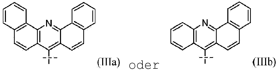 W für eine substituierte oder unsubstituierte C16-bis C48-Arylgruppe mit 2 bis 8 aromatischen Ringen oder eine substituierte oder unsubstituierte C10- bis C33-Heteroarylgruppe mit mindestens 2 bis 8 aromatischen Ringen steht und
die Substituenten aus Deuterium, C1- bis C12-Alkyl und C1- bis C12-Alkoxy ausgewählt sind. - Organische Elektrolumineszenzvorrichtung nach einem der vorhergehenden Ansprüche 1 bis 5, wobei in Formel (II):
A-W (II);
A aus der Gruppe bestehend aus Formel (IIIa) oder (IIIb) ausgewählt ist: W aus der Gruppe der Formel IV:
-L-Ar2 (IV)
ausgewählt ist, wobeiL aus Phenylen, Naphthylen und Biphenyl ausgewählt ist undAr2 aus substituiertem oder unsubstituiertem Naphthyl, Anthranyl, Chrysenyl, Pyrenyl, Benzimidazolyl, Pyridinyl, Acridinyl, Chinolinyl, Triazinyl ausgewählt istund die Substituenten aus Deuterium, C1- bis C12-Alkyl und C1- bis C12-Alkoxy ausgewählt sind. - Organische Elektrolumineszenzvorrichtung nach einem der vorhergehenden Ansprüche 1 bis 6, wobei- das Alkalimetallsalz aus der Gruppe bestehend aus LiF, LiCl, LiBr oder LiJ und vorzugsweise LiF ausgewählt ist;- der organische Alkalimetallkomplex aus der Gruppe bestehend aus einem Lithiumchinolinat, Lithiumborat, Lithiumphenolat, Lithiumpyridinolat ausgewählt ist oder ein Lithium mit einem Schiff-Base-Liganden umfasst;- vorzugsweise der Lithiumchinolinatkomplex die Formel IV, V oder VI aufweist:
 A1 bis A6 gleich oder unabhängig aus CH, CR, N, O ausgewählt sind;R gleich oder unabhängig aus Wasserstoff, Halogen, Alkyl oder Aryl oder Heteroaryl mit 1 bis 20 Kohlenstoffatomen ausgewählt ist; und weiter bevorzugt A1 bis A6 für CH stehen;- es sich bei dem organischen Liganden auf Borat-Basis vorzugsweise um ein Tetra(1H-pyrazol-1-yl)borat handelt;- es sich bei dem Phenolat vorzugsweise um ein 2-(Pyridin-2-yl)phenolat, ein 2-(Diphenylphosphoryl)phenolat, ein Imidazolphenolat oder 2-(Pyridin-yl)phenolat und weiter bevorzugt 2-(1-Phenyl-1H-benzo[d]imidazol-2-yl)phenolat handelt;- es sich bei dem Pyridinolat vorzugsweise um ein 2-(Diphenylphosphoryl)pyridin-3-olat handelt;- vorzugsweise die Lithium-Schiff-Base die Struktur 100, 101, 102 oder 103 aufweist:

- Organische Elektrolumineszenzvorrichtung nach einem der vorhergehenden Ansprüche 1 bis 7, wobei das Dipolmoment der ersten und/oder zweiten Elektronentransportmatrixverbindung ≥ 0 und ≤ 2,3 Debye, vorzugsweise ≥ 0,2 und ≤ 2,2 Debye, beträgt.
- Organische elektrolumineszierende Vorrichtung nach einem der vorhergehenden Ansprüche 1 bis 8, wobei die erste Elektronentransportschicht sandwichartig zwischen der Emissionsschicht und der zweiten Elektronentransportschicht kontaktiert und die zweite Elektronentransportschicht sandwichartig zwischen der ersten Elektronentransportschicht und der Elektroneninjektionsschicht kontaktiert.
- Organische Elektrolumineszenzvorrichtung nach einem der vorhergehenden Ansprüche 1 bis 9, wobei die organische Elektrolumineszenzvorrichtung ferner eine Elektroneninjektionsschicht (36) zwischen der zweiten Elektronentransportschicht und der Kathode umfasst.
- Verfahren zur Herstellung einer organischen Elektrolumineszenzvorrichtung (400) nach einem der vorhergehenden Ansprüche 1 bis 10, bei dem man- auf eine Anode (150) eine Lochinjektionsschicht (37), eine Lochtransportschicht (31), gegebenenfalls eine Elektronenblockierschicht (33), eine Emissionsschicht (130), eine erste Elektronentransportschicht (135), eine zweite Elektronentransportschicht (34), eine Elektroneninjektionsschicht (36) und eine Kathode (110) in der angegebenen Reihenfolge abscheidet; oder- die Schichten beginnend mit der Kathode (110) andersherum abscheidet.
- Elektronische Vorrichtung, umfassend mindestens eine organische Leuchtdiode (100) nach einem der vorhergehenden Ansprüche 1 bis 10, wobei es sich bei der elektronischen Vorrichtung mit mindestens einer organischen Leuchtdiode (100) nach einem der vorhergehenden Ansprüche 1 bis 10 vorzugsweise um eine Anzeigevorrichtung handelt.
Priority Applications (5)
| Application Number | Priority Date | Filing Date | Title |
|---|---|---|---|
| EP16195344.3A EP3312899B1 (de) | 2016-10-24 | 2016-10-24 | Elektronentransportschichtstapel für eine organische lichtemittierende diode |
| JP2017202421A JP6985883B2 (ja) | 2016-10-24 | 2017-10-19 | 有機発光ダイオードのための電子伝達層の積層体 |
| US15/788,431 US11011708B2 (en) | 2016-10-24 | 2017-10-19 | Electron transport layer stack for an organic light-emitting diode |
| KR1020170137278A KR102435687B1 (ko) | 2016-10-24 | 2017-10-23 | 유기 발광 다이오드용 전자 수송층 스택 |
| CN201711005583.7A CN107978684B (zh) | 2016-10-24 | 2017-10-24 | 用于有机发光二极管的电子传输层叠层 |
Applications Claiming Priority (1)
| Application Number | Priority Date | Filing Date | Title |
|---|---|---|---|
| EP16195344.3A EP3312899B1 (de) | 2016-10-24 | 2016-10-24 | Elektronentransportschichtstapel für eine organische lichtemittierende diode |
Publications (2)
| Publication Number | Publication Date |
|---|---|
| EP3312899A1 EP3312899A1 (de) | 2018-04-25 |
| EP3312899B1 true EP3312899B1 (de) | 2021-04-07 |
Family
ID=57208124
Family Applications (1)
| Application Number | Title | Priority Date | Filing Date |
|---|---|---|---|
| EP16195344.3A Active EP3312899B1 (de) | 2016-10-24 | 2016-10-24 | Elektronentransportschichtstapel für eine organische lichtemittierende diode |
Country Status (5)
| Country | Link |
|---|---|
| US (1) | US11011708B2 (de) |
| EP (1) | EP3312899B1 (de) |
| JP (1) | JP6985883B2 (de) |
| KR (1) | KR102435687B1 (de) |
| CN (1) | CN107978684B (de) |
Families Citing this family (18)
| Publication number | Priority date | Publication date | Assignee | Title |
|---|---|---|---|---|
| US8774918B2 (en) | 2008-10-31 | 2014-07-08 | Medtronic, Inc. | Implantable medical device crosstalk evaluation and mitigation |
| TWI577070B (zh) * | 2014-10-27 | 2017-04-01 | Lg 化學股份有限公司 | 有機電致發光元件 |
| EP3312171B1 (de) * | 2016-10-24 | 2019-07-31 | Novaled GmbH | Verbindung für elektronische vorrichtung sowie elektronische vorrichtung und anzeigevorrichtung |
| EP3556753B1 (de) * | 2018-04-18 | 2023-10-11 | Novaled GmbH | Verbindung und organische halbleitende schicht, organische elektronische vorrichtung, anzeigevorrichtung und beleuchtungsvorrichtung damit |
| EP3653619A1 (de) * | 2018-11-16 | 2020-05-20 | Novaled GmbH | Verbindung, organische elektronische vorrichtung damit sowie anzeigevorrichtung und beleuchtungsvorrichtung damit |
| WO2020159128A1 (ko) * | 2019-01-28 | 2020-08-06 | 주식회사 엘지화학 | 유기 발광 소자 |
| KR102778223B1 (ko) | 2019-01-28 | 2025-03-10 | 주식회사 엘지화학 | 유기 발광 소자 |
| EP3693352A1 (de) * | 2019-02-06 | 2020-08-12 | Novaled GmbH | Verbindung und organische halbleitende schicht, organische elektronische vorrichtung und anzeige- oder beleuchtungsvorrichtung damit |
| EP3694012B1 (de) | 2019-02-06 | 2026-02-11 | Novaled GmbH | Verfahren zur herstellung einer organischen halbleitenden schicht |
| US20220216428A1 (en) * | 2019-04-15 | 2022-07-07 | Novaled Gmbh | See addendum |
| EP3730482A1 (de) | 2019-04-24 | 2020-10-28 | Novaled GmbH | Verbindung und organische damit halbleitende schicht, organische elektronische vorrichtung und anzeigevorrichtung oder beleuchtungsvorrichtung damit |
| EP3742513A1 (de) | 2019-05-21 | 2020-11-25 | Novaled GmbH | Organische leuchtdiode |
| CN110183381A (zh) * | 2019-06-28 | 2019-08-30 | 上海天马有机发光显示技术有限公司 | 一种化合物、oled显示面板以及电子设备 |
| EP3835295B1 (de) * | 2019-12-10 | 2026-07-01 | Novaled GmbH | Acridin-verbindung und organische halbleitende schicht, organische elektronische vorrichtung und anzeigevorrichtung damit |
| EP3920249A1 (de) | 2020-06-03 | 2021-12-08 | Novaled GmbH | Verbindung, zwischenprodukt der verbindung, verfahren zur herstellung der verbindung, organisches halbleitendes material mit der verbindung, organische elektronische vorrichtung damit und anzeigevorrichtung und beleuchtungsvorrichtung damit |
| EP3923363B1 (de) * | 2020-06-12 | 2026-02-11 | Novaled GmbH | Organische leuchtdiode und vorrichtung damit |
| EP3923364B1 (de) * | 2020-06-12 | 2025-09-17 | Novaled GmbH | Organische leuchtdiode und vorrichtung damit |
| EP4141980A1 (de) * | 2021-08-24 | 2023-03-01 | Novaled GmbH | Organische leuchtdiode und verbindung zur verwendung darin |
Family Cites Families (25)
| Publication number | Priority date | Publication date | Assignee | Title |
|---|---|---|---|---|
| US6800380B2 (en) | 1998-06-23 | 2004-10-05 | Nessdisplay Co., Ltd. | Organometallic luminescent materials and organic electroluminescent device containing same |
| JP3945123B2 (ja) | 2000-04-10 | 2007-07-18 | 三菱化学株式会社 | 有機電界発光素子 |
| JP4003824B2 (ja) * | 2001-07-11 | 2007-11-07 | 富士フイルム株式会社 | 発光素子 |
| WO2003007658A2 (en) * | 2001-07-11 | 2003-01-23 | Fuji Photo Film Co., Ltd. | Light-emitting device and aromatic compound |
| US20040209116A1 (en) * | 2003-04-21 | 2004-10-21 | Xiaofan Ren | Organic light emitting devices with wide gap host materials |
| JP2006279014A (ja) * | 2004-09-15 | 2006-10-12 | Fuji Photo Film Co Ltd | 有機電界発光素子 |
| US8049407B2 (en) * | 2004-09-15 | 2011-11-01 | Fujifilm Corporation | Organic electroluminescent element including blue phosphorescent luminescent material |
| KR20070061829A (ko) * | 2004-09-22 | 2007-06-14 | 도꾸리쯔교세이호징 가가꾸 기쥬쯔 신꼬 기꼬 | 유기전계발광소자 |
| DE102007014048B4 (de) | 2006-03-21 | 2013-02-21 | Novaled Ag | Mischung aus Matrixmaterial und Dotierungsmaterial, sowie Verfahren zum Herstellen einer Schicht aus dotiertem organischen Material |
| DE502006000749D1 (de) | 2006-03-21 | 2008-06-19 | Novaled Ag | Heterocyclisches Radikal oder Diradikal, deren Dimere, Oligomere, Polymere, Dispiroverbindungen und Polycyclen, deren Verwendung, organisches halbleitendes Material sowie elektronisches Bauelement |
| EP1837927A1 (de) | 2006-03-22 | 2007-09-26 | Novaled AG | Verwendung von heterocyclischen Radikalen zur Dotierung von organischen Halbleitern |
| JP2008195623A (ja) | 2007-02-08 | 2008-08-28 | Chemiprokasei Kaisha Ltd | 新規な複素環含有ヒドロキシフェニル金属誘導体およびそれを用いた電子注入材料、電子輸送材料および有機エレクトロルミネッセンス素子 |
| WO2009054253A1 (ja) * | 2007-10-26 | 2009-04-30 | Konica Minolta Holdings, Inc. | 有機エレクトロルミネッセンス素子、表示装置及び照明装置 |
| EP2395571B1 (de) | 2010-06-10 | 2013-12-04 | Novaled AG | Eine organische Vorrichtung umfassend ein organisches halbleitendes Material |
| EP4242216B1 (de) | 2011-06-22 | 2025-11-12 | Novaled GmbH | Elektronische vorrichtung und verbindung |
| JP6170501B2 (ja) * | 2011-11-30 | 2017-07-26 | ノヴァレッド ゲーエムベーハー | ディスプレイ |
| KR102051360B1 (ko) | 2011-11-30 | 2019-12-03 | 노발레드 게엠베하 | 유기 전자 소자 |
| JP6165760B2 (ja) | 2011-11-30 | 2017-07-19 | ノヴァレッド ゲーエムベーハー | 有機電子装置 |
| WO2014141725A1 (ja) * | 2013-03-15 | 2014-09-18 | 出光興産株式会社 | アントラセン誘導体及びそれを用いた有機エレクトロルミネッセンス素子 |
| US9553274B2 (en) * | 2013-07-16 | 2017-01-24 | Universal Display Corporation | Organic electroluminescent materials and devices |
| KR20150014778A (ko) * | 2013-07-30 | 2015-02-09 | 삼성디스플레이 주식회사 | 유기 발광 소자 |
| KR20150096020A (ko) * | 2014-02-13 | 2015-08-24 | 삼성디스플레이 주식회사 | 유기 발광 소자 |
| EP3035400B1 (de) * | 2014-12-17 | 2019-10-23 | Novaled GmbH | Organische Leuchtdiode mit Elektronentransportschichten mit unterschiedlichen Matrixverbindungen |
| KR101888934B1 (ko) * | 2015-04-24 | 2018-08-16 | 삼성에스디아이 주식회사 | 유기 광전자 소자용 화합물, 유기 광전자 소자 및 표시장치 |
| EP3182478B1 (de) * | 2015-12-18 | 2018-11-28 | Novaled GmbH | Elektroneninjektionsschicht für eine organische leuchtdiode (oled) |
-
2016
- 2016-10-24 EP EP16195344.3A patent/EP3312899B1/de active Active
-
2017
- 2017-10-19 US US15/788,431 patent/US11011708B2/en active Active
- 2017-10-19 JP JP2017202421A patent/JP6985883B2/ja active Active
- 2017-10-23 KR KR1020170137278A patent/KR102435687B1/ko active Active
- 2017-10-24 CN CN201711005583.7A patent/CN107978684B/zh active Active
Non-Patent Citations (1)
| Title |
|---|
| None * |
Also Published As
| Publication number | Publication date |
|---|---|
| JP2018117112A (ja) | 2018-07-26 |
| KR20180044821A (ko) | 2018-05-03 |
| US11011708B2 (en) | 2021-05-18 |
| JP6985883B2 (ja) | 2021-12-22 |
| KR102435687B1 (ko) | 2022-08-23 |
| CN107978684A (zh) | 2018-05-01 |
| EP3312899A1 (de) | 2018-04-25 |
| CN107978684B (zh) | 2022-08-23 |
| US20180114920A1 (en) | 2018-04-26 |
Similar Documents
| Publication | Publication Date | Title |
|---|---|---|
| US11011708B2 (en) | Electron transport layer stack for an organic light-emitting diode | |
| KR102677419B1 (ko) | 정공 주입층 및 영가 금속을 함유하는 전자 주입층을 포함하는 유기 전계발광 장치 | |
| EP3312895B1 (de) | Organisches halbleitermaterial mit einem elektrischen n-dotierstoff sowie elektronentransportmatrix und elektronische vorrichtung mit dem halbleitermaterial | |
| EP3689867B1 (de) | Zusammensetzung, organische halbleiterschicht und elektronische vorrichtung | |
| EP3898606B1 (de) | Verbindung und organische halbleitende schicht, organische elektronische vorrichtung und anzeigevorrichtung | |
| US11524952B2 (en) | Compound and organic semiconducting layer, organic electronic device, display device and lighting device comprising the same | |
| EP3503240B1 (de) | Organische halbleiterschicht | |
| US11145826B2 (en) | Compound for electronic device and electronic device and display device | |
| KR102628725B1 (ko) | 트리아진기, 플루오렌기 및 헤테로-플루오렌기를 포함하는 화합물 | |
| KR102583049B1 (ko) | 전자 장치 및 디스플레이 장치에 사용하기 위한 아크리딘 화합물 | |
| EP3527557A1 (de) | N-heteroarylen-verbindungen | |
| KR102639012B1 (ko) | 트리아진기, 플루오렌기 및 아릴기를 포함하는 화합물 | |
| EP3693352A1 (de) | Verbindung und organische halbleitende schicht, organische elektronische vorrichtung und anzeige- oder beleuchtungsvorrichtung damit | |
| KR102685005B1 (ko) | 트리아진기, 플루오렌기 및 아릴기를 포함하는 화합물 |
Legal Events
| Date | Code | Title | Description |
|---|---|---|---|
| PUAI | Public reference made under article 153(3) epc to a published international application that has entered the european phase |
Free format text: ORIGINAL CODE: 0009012 |
|
| STAA | Information on the status of an ep patent application or granted ep patent |
Free format text: STATUS: THE APPLICATION HAS BEEN PUBLISHED |
|
| AK | Designated contracting states |
Kind code of ref document: A1 Designated state(s): AL AT BE BG CH CY CZ DE DK EE ES FI FR GB GR HR HU IE IS IT LI LT LU LV MC MK MT NL NO PL PT RO RS SE SI SK SM TR |
|
| AX | Request for extension of the european patent |
Extension state: BA ME |
|
| STAA | Information on the status of an ep patent application or granted ep patent |
Free format text: STATUS: REQUEST FOR EXAMINATION WAS MADE |
|
| 17P | Request for examination filed |
Effective date: 20181024 |
|
| RBV | Designated contracting states (corrected) |
Designated state(s): AL AT BE BG CH CY CZ DE DK EE ES FI FR GB GR HR HU IE IS IT LI LT LU LV MC MK MT NL NO PL PT RO RS SE SI SK SM TR |
|
| RAP1 | Party data changed (applicant data changed or rights of an application transferred) |
Owner name: SAMSUNG SDI CO., LTD. Owner name: NOVALED GMBH |
|
| GRAJ | Information related to disapproval of communication of intention to grant by the applicant or resumption of examination proceedings by the epo deleted |
Free format text: ORIGINAL CODE: EPIDOSDIGR1 |
|
| STAA | Information on the status of an ep patent application or granted ep patent |
Free format text: STATUS: GRANT OF PATENT IS INTENDED |
|
| GRAP | Despatch of communication of intention to grant a patent |
Free format text: ORIGINAL CODE: EPIDOSNIGR1 |
|
| INTG | Intention to grant announced |
Effective date: 20201111 |
|
| GRAS | Grant fee paid |
Free format text: ORIGINAL CODE: EPIDOSNIGR3 |
|
| GRAA | (expected) grant |
Free format text: ORIGINAL CODE: 0009210 |
|
| STAA | Information on the status of an ep patent application or granted ep patent |
Free format text: STATUS: THE PATENT HAS BEEN GRANTED |
|
| AK | Designated contracting states |
Kind code of ref document: B1 Designated state(s): AL AT BE BG CH CY CZ DE DK EE ES FI FR GB GR HR HU IE IS IT LI LT LU LV MC MK MT NL NO PL PT RO RS SE SI SK SM TR |
|
| REG | Reference to a national code |
Ref country code: GB Ref legal event code: FG4D |
|
| REG | Reference to a national code |
Ref country code: AT Ref legal event code: REF Ref document number: 1380824 Country of ref document: AT Kind code of ref document: T Effective date: 20210415 Ref country code: CH Ref legal event code: EP |
|
| REG | Reference to a national code |
Ref country code: DE Ref legal event code: R096 Ref document number: 602016055555 Country of ref document: DE |
|
| REG | Reference to a national code |
Ref country code: IE Ref legal event code: FG4D |
|
| REG | Reference to a national code |
Ref country code: LT Ref legal event code: MG9D |
|
| REG | Reference to a national code |
Ref country code: NL Ref legal event code: MP Effective date: 20210407 Ref country code: AT Ref legal event code: MK05 Ref document number: 1380824 Country of ref document: AT Kind code of ref document: T Effective date: 20210407 |
|
| PG25 | Lapsed in a contracting state [announced via postgrant information from national office to epo] |
Ref country code: HR Free format text: LAPSE BECAUSE OF FAILURE TO SUBMIT A TRANSLATION OF THE DESCRIPTION OR TO PAY THE FEE WITHIN THE PRESCRIBED TIME-LIMIT Effective date: 20210407 Ref country code: BG Free format text: LAPSE BECAUSE OF FAILURE TO SUBMIT A TRANSLATION OF THE DESCRIPTION OR TO PAY THE FEE WITHIN THE PRESCRIBED TIME-LIMIT Effective date: 20210707 Ref country code: AT Free format text: LAPSE BECAUSE OF FAILURE TO SUBMIT A TRANSLATION OF THE DESCRIPTION OR TO PAY THE FEE WITHIN THE PRESCRIBED TIME-LIMIT Effective date: 20210407 Ref country code: FI Free format text: LAPSE BECAUSE OF FAILURE TO SUBMIT A TRANSLATION OF THE DESCRIPTION OR TO PAY THE FEE WITHIN THE PRESCRIBED TIME-LIMIT Effective date: 20210407 Ref country code: LT Free format text: LAPSE BECAUSE OF FAILURE TO SUBMIT A TRANSLATION OF THE DESCRIPTION OR TO PAY THE FEE WITHIN THE PRESCRIBED TIME-LIMIT Effective date: 20210407 Ref country code: NL Free format text: LAPSE BECAUSE OF FAILURE TO SUBMIT A TRANSLATION OF THE DESCRIPTION OR TO PAY THE FEE WITHIN THE PRESCRIBED TIME-LIMIT Effective date: 20210407 |
|
| PG25 | Lapsed in a contracting state [announced via postgrant information from national office to epo] |
Ref country code: NO Free format text: LAPSE BECAUSE OF FAILURE TO SUBMIT A TRANSLATION OF THE DESCRIPTION OR TO PAY THE FEE WITHIN THE PRESCRIBED TIME-LIMIT Effective date: 20210707 Ref country code: PT Free format text: LAPSE BECAUSE OF FAILURE TO SUBMIT A TRANSLATION OF THE DESCRIPTION OR TO PAY THE FEE WITHIN THE PRESCRIBED TIME-LIMIT Effective date: 20210809 Ref country code: PL Free format text: LAPSE BECAUSE OF FAILURE TO SUBMIT A TRANSLATION OF THE DESCRIPTION OR TO PAY THE FEE WITHIN THE PRESCRIBED TIME-LIMIT Effective date: 20210407 Ref country code: RS Free format text: LAPSE BECAUSE OF FAILURE TO SUBMIT A TRANSLATION OF THE DESCRIPTION OR TO PAY THE FEE WITHIN THE PRESCRIBED TIME-LIMIT Effective date: 20210407 Ref country code: SE Free format text: LAPSE BECAUSE OF FAILURE TO SUBMIT A TRANSLATION OF THE DESCRIPTION OR TO PAY THE FEE WITHIN THE PRESCRIBED TIME-LIMIT Effective date: 20210407 Ref country code: IS Free format text: LAPSE BECAUSE OF FAILURE TO SUBMIT A TRANSLATION OF THE DESCRIPTION OR TO PAY THE FEE WITHIN THE PRESCRIBED TIME-LIMIT Effective date: 20210807 Ref country code: GR Free format text: LAPSE BECAUSE OF FAILURE TO SUBMIT A TRANSLATION OF THE DESCRIPTION OR TO PAY THE FEE WITHIN THE PRESCRIBED TIME-LIMIT Effective date: 20210708 Ref country code: LV Free format text: LAPSE BECAUSE OF FAILURE TO SUBMIT A TRANSLATION OF THE DESCRIPTION OR TO PAY THE FEE WITHIN THE PRESCRIBED TIME-LIMIT Effective date: 20210407 |
|
| REG | Reference to a national code |
Ref country code: DE Ref legal event code: R097 Ref document number: 602016055555 Country of ref document: DE |
|
| PG25 | Lapsed in a contracting state [announced via postgrant information from national office to epo] |
Ref country code: DK Free format text: LAPSE BECAUSE OF FAILURE TO SUBMIT A TRANSLATION OF THE DESCRIPTION OR TO PAY THE FEE WITHIN THE PRESCRIBED TIME-LIMIT Effective date: 20210407 Ref country code: CZ Free format text: LAPSE BECAUSE OF FAILURE TO SUBMIT A TRANSLATION OF THE DESCRIPTION OR TO PAY THE FEE WITHIN THE PRESCRIBED TIME-LIMIT Effective date: 20210407 Ref country code: EE Free format text: LAPSE BECAUSE OF FAILURE TO SUBMIT A TRANSLATION OF THE DESCRIPTION OR TO PAY THE FEE WITHIN THE PRESCRIBED TIME-LIMIT Effective date: 20210407 Ref country code: SK Free format text: LAPSE BECAUSE OF FAILURE TO SUBMIT A TRANSLATION OF THE DESCRIPTION OR TO PAY THE FEE WITHIN THE PRESCRIBED TIME-LIMIT Effective date: 20210407 Ref country code: SM Free format text: LAPSE BECAUSE OF FAILURE TO SUBMIT A TRANSLATION OF THE DESCRIPTION OR TO PAY THE FEE WITHIN THE PRESCRIBED TIME-LIMIT Effective date: 20210407 Ref country code: RO Free format text: LAPSE BECAUSE OF FAILURE TO SUBMIT A TRANSLATION OF THE DESCRIPTION OR TO PAY THE FEE WITHIN THE PRESCRIBED TIME-LIMIT Effective date: 20210407 Ref country code: ES Free format text: LAPSE BECAUSE OF FAILURE TO SUBMIT A TRANSLATION OF THE DESCRIPTION OR TO PAY THE FEE WITHIN THE PRESCRIBED TIME-LIMIT Effective date: 20210407 |
|
| PLBE | No opposition filed within time limit |
Free format text: ORIGINAL CODE: 0009261 |
|
| STAA | Information on the status of an ep patent application or granted ep patent |
Free format text: STATUS: NO OPPOSITION FILED WITHIN TIME LIMIT |
|
| 26N | No opposition filed |
Effective date: 20220110 |
|
| REG | Reference to a national code |
Ref country code: CH Ref legal event code: PL |
|
| PG25 | Lapsed in a contracting state [announced via postgrant information from national office to epo] |
Ref country code: IS Free format text: LAPSE BECAUSE OF FAILURE TO SUBMIT A TRANSLATION OF THE DESCRIPTION OR TO PAY THE FEE WITHIN THE PRESCRIBED TIME-LIMIT Effective date: 20210807 Ref country code: AL Free format text: LAPSE BECAUSE OF FAILURE TO SUBMIT A TRANSLATION OF THE DESCRIPTION OR TO PAY THE FEE WITHIN THE PRESCRIBED TIME-LIMIT Effective date: 20210407 |
|
| REG | Reference to a national code |
Ref country code: BE Ref legal event code: MM Effective date: 20211031 |
|
| GBPC | Gb: european patent ceased through non-payment of renewal fee |
Effective date: 20211024 |
|
| PG25 | Lapsed in a contracting state [announced via postgrant information from national office to epo] |
Ref country code: MC Free format text: LAPSE BECAUSE OF FAILURE TO SUBMIT A TRANSLATION OF THE DESCRIPTION OR TO PAY THE FEE WITHIN THE PRESCRIBED TIME-LIMIT Effective date: 20210407 |
|
| PG25 | Lapsed in a contracting state [announced via postgrant information from national office to epo] |
Ref country code: LU Free format text: LAPSE BECAUSE OF NON-PAYMENT OF DUE FEES Effective date: 20211024 Ref country code: IT Free format text: LAPSE BECAUSE OF FAILURE TO SUBMIT A TRANSLATION OF THE DESCRIPTION OR TO PAY THE FEE WITHIN THE PRESCRIBED TIME-LIMIT Effective date: 20210407 Ref country code: GB Free format text: LAPSE BECAUSE OF NON-PAYMENT OF DUE FEES Effective date: 20211024 Ref country code: BE Free format text: LAPSE BECAUSE OF NON-PAYMENT OF DUE FEES Effective date: 20211031 |
|
| PG25 | Lapsed in a contracting state [announced via postgrant information from national office to epo] |
Ref country code: LI Free format text: LAPSE BECAUSE OF NON-PAYMENT OF DUE FEES Effective date: 20211031 Ref country code: CH Free format text: LAPSE BECAUSE OF NON-PAYMENT OF DUE FEES Effective date: 20211031 |
|
| PG25 | Lapsed in a contracting state [announced via postgrant information from national office to epo] |
Ref country code: FR Free format text: LAPSE BECAUSE OF NON-PAYMENT OF DUE FEES Effective date: 20211031 |
|
| PG25 | Lapsed in a contracting state [announced via postgrant information from national office to epo] |
Ref country code: IE Free format text: LAPSE BECAUSE OF NON-PAYMENT OF DUE FEES Effective date: 20211024 |
|
| REG | Reference to a national code |
Ref country code: DE Ref legal event code: R079 Ref document number: 602016055555 Country of ref document: DE Free format text: PREVIOUS MAIN CLASS: H01L0051520000 Ipc: H10K0050800000 |
|
| PG25 | Lapsed in a contracting state [announced via postgrant information from national office to epo] |
Ref country code: HU Free format text: LAPSE BECAUSE OF FAILURE TO SUBMIT A TRANSLATION OF THE DESCRIPTION OR TO PAY THE FEE WITHIN THE PRESCRIBED TIME-LIMIT; INVALID AB INITIO Effective date: 20161024 |
|
| PG25 | Lapsed in a contracting state [announced via postgrant information from national office to epo] |
Ref country code: CY Free format text: LAPSE BECAUSE OF FAILURE TO SUBMIT A TRANSLATION OF THE DESCRIPTION OR TO PAY THE FEE WITHIN THE PRESCRIBED TIME-LIMIT Effective date: 20210407 |
|
| P01 | Opt-out of the competence of the unified patent court (upc) registered |
Effective date: 20230526 |
|
| PG25 | Lapsed in a contracting state [announced via postgrant information from national office to epo] |
Ref country code: MK Free format text: LAPSE BECAUSE OF FAILURE TO SUBMIT A TRANSLATION OF THE DESCRIPTION OR TO PAY THE FEE WITHIN THE PRESCRIBED TIME-LIMIT Effective date: 20210407 |
|
| PG25 | Lapsed in a contracting state [announced via postgrant information from national office to epo] |
Ref country code: TR Free format text: LAPSE BECAUSE OF FAILURE TO SUBMIT A TRANSLATION OF THE DESCRIPTION OR TO PAY THE FEE WITHIN THE PRESCRIBED TIME-LIMIT Effective date: 20210407 |
|
| PG25 | Lapsed in a contracting state [announced via postgrant information from national office to epo] |
Ref country code: MT Free format text: LAPSE BECAUSE OF FAILURE TO SUBMIT A TRANSLATION OF THE DESCRIPTION OR TO PAY THE FEE WITHIN THE PRESCRIBED TIME-LIMIT Effective date: 20210407 |
|
| PGFP | Annual fee paid to national office [announced via postgrant information from national office to epo] |
Ref country code: DE Payment date: 20250827 Year of fee payment: 10 |