EP3312899B1 - Empilement de couches de transport d'électrons pour une diode électroluminescente organique - Google Patents
Empilement de couches de transport d'électrons pour une diode électroluminescente organique Download PDFInfo
- Publication number
- EP3312899B1 EP3312899B1 EP16195344.3A EP16195344A EP3312899B1 EP 3312899 B1 EP3312899 B1 EP 3312899B1 EP 16195344 A EP16195344 A EP 16195344A EP 3312899 B1 EP3312899 B1 EP 3312899B1
- Authority
- EP
- European Patent Office
- Prior art keywords
- group
- substituted
- unsubstituted
- electron transport
- transport layer
- Prior art date
- Legal status (The legal status is an assumption and is not a legal conclusion. Google has not performed a legal analysis and makes no representation as to the accuracy of the status listed.)
- Active
Links
- 0 CC(*)CC(C)([C@@]([C@@](C)CNCC1C=C(*)C*C1)C=CIC(C)C(C)[C@]1[C@](C)C1)S Chemical compound CC(*)CC(C)([C@@]([C@@](C)CNCC1C=C(*)C*C1)C=CIC(C)C(C)[C@]1[C@](C)C1)S 0.000 description 4
- LCLULYKHEHNZBI-UHFFFAOYSA-N [I-]c1c(ccc2ccccc22)c2nc2c1ccc1ccccc21 Chemical compound [I-]c1c(ccc2ccccc22)c2nc2c1ccc1ccccc21 LCLULYKHEHNZBI-UHFFFAOYSA-N 0.000 description 1
- CGMVNBNIECPAFE-UHFFFAOYSA-N [I-]c1c(ccc2ccccc22)c2nc2ccccc12 Chemical compound [I-]c1c(ccc2ccccc22)c2nc2ccccc12 CGMVNBNIECPAFE-UHFFFAOYSA-N 0.000 description 1
- XQQKCSNLLGHJQH-UHFFFAOYSA-N c(cc1)cc(cc2)c1c1c2c(-c2cc(-c3cc(-c4cnccc4)cc(-c4cnccc4)c3)ccc2)c(ccc2ccccc22)c2n1 Chemical compound c(cc1)cc(cc2)c1c1c2c(-c2cc(-c3cc(-c4cnccc4)cc(-c4cnccc4)c3)ccc2)c(ccc2ccccc22)c2n1 XQQKCSNLLGHJQH-UHFFFAOYSA-N 0.000 description 1
- KRGZCOASGYWGOT-UHFFFAOYSA-N c(cc1)cc(cc2)c1c1c2c(-c2cc(-c3ccncc3)ccc2)c(ccc2ccccc22)c2n1 Chemical compound c(cc1)cc(cc2)c1c1c2c(-c2cc(-c3ccncc3)ccc2)c(ccc2ccccc22)c2n1 KRGZCOASGYWGOT-UHFFFAOYSA-N 0.000 description 1
- JIYIQUYALSYZSK-UHFFFAOYSA-N c(cc1cc2)ccc1c1c2c(-c2cccc(-c3cccc(-c4cccc5c4nccc5)c3)c2)c(ccc2ccccc22)c2n1 Chemical compound c(cc1cc2)ccc1c1c2c(-c2cccc(-c3cccc(-c4cccc5c4nccc5)c3)c2)c(ccc2ccccc22)c2n1 JIYIQUYALSYZSK-UHFFFAOYSA-N 0.000 description 1
Images

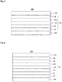
Classifications
-
- C—CHEMISTRY; METALLURGY
- C07—ORGANIC CHEMISTRY
- C07D—HETEROCYCLIC COMPOUNDS
- C07D221/00—Heterocyclic compounds containing six-membered rings having one nitrogen atom as the only ring hetero atom, not provided for by groups C07D211/00 - C07D219/00
- C07D221/02—Heterocyclic compounds containing six-membered rings having one nitrogen atom as the only ring hetero atom, not provided for by groups C07D211/00 - C07D219/00 condensed with carbocyclic rings or ring systems
- C07D221/04—Ortho- or peri-condensed ring systems
- C07D221/18—Ring systems of four or more rings
-
- H—ELECTRICITY
- H10—SEMICONDUCTOR DEVICES; ELECTRIC SOLID-STATE DEVICES NOT OTHERWISE PROVIDED FOR
- H10K—ORGANIC ELECTRIC SOLID-STATE DEVICES
- H10K50/00—Organic light-emitting devices
- H10K50/10—OLEDs or polymer light-emitting diodes [PLED]
- H10K50/14—Carrier transporting layers
- H10K50/16—Electron transporting layers
- H10K50/166—Electron transporting layers comprising a multilayered structure
-
- C—CHEMISTRY; METALLURGY
- C07—ORGANIC CHEMISTRY
- C07D—HETEROCYCLIC COMPOUNDS
- C07D251/00—Heterocyclic compounds containing 1,3,5-triazine rings
- C07D251/02—Heterocyclic compounds containing 1,3,5-triazine rings not condensed with other rings
- C07D251/12—Heterocyclic compounds containing 1,3,5-triazine rings not condensed with other rings having three double bonds between ring members or between ring members and non-ring members
- C07D251/14—Heterocyclic compounds containing 1,3,5-triazine rings not condensed with other rings having three double bonds between ring members or between ring members and non-ring members with hydrogen or carbon atoms directly attached to at least one ring carbon atom
- C07D251/24—Heterocyclic compounds containing 1,3,5-triazine rings not condensed with other rings having three double bonds between ring members or between ring members and non-ring members with hydrogen or carbon atoms directly attached to at least one ring carbon atom to three ring carbon atoms
-
- C—CHEMISTRY; METALLURGY
- C07—ORGANIC CHEMISTRY
- C07D—HETEROCYCLIC COMPOUNDS
- C07D401/00—Heterocyclic compounds containing two or more hetero rings, having nitrogen atoms as the only ring hetero atoms, at least one ring being a six-membered ring with only one nitrogen atom
- C07D401/02—Heterocyclic compounds containing two or more hetero rings, having nitrogen atoms as the only ring hetero atoms, at least one ring being a six-membered ring with only one nitrogen atom containing two hetero rings
- C07D401/10—Heterocyclic compounds containing two or more hetero rings, having nitrogen atoms as the only ring hetero atoms, at least one ring being a six-membered ring with only one nitrogen atom containing two hetero rings linked by a carbon chain containing aromatic rings
-
- C—CHEMISTRY; METALLURGY
- C07—ORGANIC CHEMISTRY
- C07D—HETEROCYCLIC COMPOUNDS
- C07D495/00—Heterocyclic compounds containing in the condensed system at least one hetero ring having sulfur atoms as the only ring hetero atoms
- C07D495/02—Heterocyclic compounds containing in the condensed system at least one hetero ring having sulfur atoms as the only ring hetero atoms in which the condensed system contains two hetero rings
- C07D495/04—Ortho-condensed systems
-
- H—ELECTRICITY
- H10—SEMICONDUCTOR DEVICES; ELECTRIC SOLID-STATE DEVICES NOT OTHERWISE PROVIDED FOR
- H10K—ORGANIC ELECTRIC SOLID-STATE DEVICES
- H10K50/00—Organic light-emitting devices
- H10K50/10—OLEDs or polymer light-emitting diodes [PLED]
- H10K50/11—OLEDs or polymer light-emitting diodes [PLED] characterised by the electroluminescent [EL] layers
- H10K50/12—OLEDs or polymer light-emitting diodes [PLED] characterised by the electroluminescent [EL] layers comprising dopants
-
- H—ELECTRICITY
- H10—SEMICONDUCTOR DEVICES; ELECTRIC SOLID-STATE DEVICES NOT OTHERWISE PROVIDED FOR
- H10K—ORGANIC ELECTRIC SOLID-STATE DEVICES
- H10K50/00—Organic light-emitting devices
- H10K50/10—OLEDs or polymer light-emitting diodes [PLED]
- H10K50/14—Carrier transporting layers
- H10K50/15—Hole transporting layers
-
- H—ELECTRICITY
- H10—SEMICONDUCTOR DEVICES; ELECTRIC SOLID-STATE DEVICES NOT OTHERWISE PROVIDED FOR
- H10K—ORGANIC ELECTRIC SOLID-STATE DEVICES
- H10K50/00—Organic light-emitting devices
- H10K50/10—OLEDs or polymer light-emitting diodes [PLED]
- H10K50/17—Carrier injection layers
-
- H—ELECTRICITY
- H10—SEMICONDUCTOR DEVICES; ELECTRIC SOLID-STATE DEVICES NOT OTHERWISE PROVIDED FOR
- H10K—ORGANIC ELECTRIC SOLID-STATE DEVICES
- H10K50/00—Organic light-emitting devices
- H10K50/10—OLEDs or polymer light-emitting diodes [PLED]
- H10K50/18—Carrier blocking layers
-
- H—ELECTRICITY
- H10—SEMICONDUCTOR DEVICES; ELECTRIC SOLID-STATE DEVICES NOT OTHERWISE PROVIDED FOR
- H10K—ORGANIC ELECTRIC SOLID-STATE DEVICES
- H10K59/00—Integrated devices, or assemblies of multiple devices, comprising at least one organic light-emitting element covered by group H10K50/00
-
- H—ELECTRICITY
- H10—SEMICONDUCTOR DEVICES; ELECTRIC SOLID-STATE DEVICES NOT OTHERWISE PROVIDED FOR
- H10K—ORGANIC ELECTRIC SOLID-STATE DEVICES
- H10K85/00—Organic materials used in the body or electrodes of devices covered by this subclass
- H10K85/60—Organic compounds having low molecular weight
- H10K85/615—Polycyclic condensed aromatic hydrocarbons, e.g. anthracene
-
- H—ELECTRICITY
- H10—SEMICONDUCTOR DEVICES; ELECTRIC SOLID-STATE DEVICES NOT OTHERWISE PROVIDED FOR
- H10K—ORGANIC ELECTRIC SOLID-STATE DEVICES
- H10K85/00—Organic materials used in the body or electrodes of devices covered by this subclass
- H10K85/60—Organic compounds having low molecular weight
- H10K85/615—Polycyclic condensed aromatic hydrocarbons, e.g. anthracene
- H10K85/622—Polycyclic condensed aromatic hydrocarbons, e.g. anthracene containing four rings, e.g. pyrene
-
- H—ELECTRICITY
- H10—SEMICONDUCTOR DEVICES; ELECTRIC SOLID-STATE DEVICES NOT OTHERWISE PROVIDED FOR
- H10K—ORGANIC ELECTRIC SOLID-STATE DEVICES
- H10K85/00—Organic materials used in the body or electrodes of devices covered by this subclass
- H10K85/60—Organic compounds having low molecular weight
- H10K85/649—Aromatic compounds comprising a hetero atom
-
- H—ELECTRICITY
- H10—SEMICONDUCTOR DEVICES; ELECTRIC SOLID-STATE DEVICES NOT OTHERWISE PROVIDED FOR
- H10K—ORGANIC ELECTRIC SOLID-STATE DEVICES
- H10K85/00—Organic materials used in the body or electrodes of devices covered by this subclass
- H10K85/60—Organic compounds having low molecular weight
- H10K85/649—Aromatic compounds comprising a hetero atom
- H10K85/654—Aromatic compounds comprising a hetero atom comprising only nitrogen as heteroatom
-
- H—ELECTRICITY
- H10—SEMICONDUCTOR DEVICES; ELECTRIC SOLID-STATE DEVICES NOT OTHERWISE PROVIDED FOR
- H10K—ORGANIC ELECTRIC SOLID-STATE DEVICES
- H10K85/00—Organic materials used in the body or electrodes of devices covered by this subclass
- H10K85/60—Organic compounds having low molecular weight
- H10K85/649—Aromatic compounds comprising a hetero atom
- H10K85/657—Polycyclic condensed heteroaromatic hydrocarbons
-
- H—ELECTRICITY
- H10—SEMICONDUCTOR DEVICES; ELECTRIC SOLID-STATE DEVICES NOT OTHERWISE PROVIDED FOR
- H10K—ORGANIC ELECTRIC SOLID-STATE DEVICES
- H10K85/00—Organic materials used in the body or electrodes of devices covered by this subclass
- H10K85/60—Organic compounds having low molecular weight
- H10K85/649—Aromatic compounds comprising a hetero atom
- H10K85/657—Polycyclic condensed heteroaromatic hydrocarbons
- H10K85/6572—Polycyclic condensed heteroaromatic hydrocarbons comprising only nitrogen in the heteroaromatic polycondensed ring system, e.g. phenanthroline or carbazole
-
- H—ELECTRICITY
- H10—SEMICONDUCTOR DEVICES; ELECTRIC SOLID-STATE DEVICES NOT OTHERWISE PROVIDED FOR
- H10K—ORGANIC ELECTRIC SOLID-STATE DEVICES
- H10K2101/00—Properties of the organic materials covered by group H10K85/00
- H10K2101/10—Triplet emission
-
- H—ELECTRICITY
- H10—SEMICONDUCTOR DEVICES; ELECTRIC SOLID-STATE DEVICES NOT OTHERWISE PROVIDED FOR
- H10K—ORGANIC ELECTRIC SOLID-STATE DEVICES
- H10K50/00—Organic light-emitting devices
- H10K50/10—OLEDs or polymer light-emitting diodes [PLED]
- H10K50/11—OLEDs or polymer light-emitting diodes [PLED] characterised by the electroluminescent [EL] layers
-
- H—ELECTRICITY
- H10—SEMICONDUCTOR DEVICES; ELECTRIC SOLID-STATE DEVICES NOT OTHERWISE PROVIDED FOR
- H10K—ORGANIC ELECTRIC SOLID-STATE DEVICES
- H10K50/00—Organic light-emitting devices
- H10K50/10—OLEDs or polymer light-emitting diodes [PLED]
- H10K50/14—Carrier transporting layers
- H10K50/16—Electron transporting layers
- H10K50/165—Electron transporting layers comprising dopants
-
- H—ELECTRICITY
- H10—SEMICONDUCTOR DEVICES; ELECTRIC SOLID-STATE DEVICES NOT OTHERWISE PROVIDED FOR
- H10K—ORGANIC ELECTRIC SOLID-STATE DEVICES
- H10K59/00—Integrated devices, or assemblies of multiple devices, comprising at least one organic light-emitting element covered by group H10K50/00
- H10K59/10—OLED displays
-
- H—ELECTRICITY
- H10—SEMICONDUCTOR DEVICES; ELECTRIC SOLID-STATE DEVICES NOT OTHERWISE PROVIDED FOR
- H10K—ORGANIC ELECTRIC SOLID-STATE DEVICES
- H10K71/00—Manufacture or treatment specially adapted for the organic devices covered by this subclass
-
- H—ELECTRICITY
- H10—SEMICONDUCTOR DEVICES; ELECTRIC SOLID-STATE DEVICES NOT OTHERWISE PROVIDED FOR
- H10K—ORGANIC ELECTRIC SOLID-STATE DEVICES
- H10K71/00—Manufacture or treatment specially adapted for the organic devices covered by this subclass
- H10K71/40—Thermal treatment, e.g. annealing in the presence of a solvent vapour
-
- H—ELECTRICITY
- H10—SEMICONDUCTOR DEVICES; ELECTRIC SOLID-STATE DEVICES NOT OTHERWISE PROVIDED FOR
- H10K—ORGANIC ELECTRIC SOLID-STATE DEVICES
- H10K85/00—Organic materials used in the body or electrodes of devices covered by this subclass
- H10K85/30—Coordination compounds
Definitions
- OLEDs Organic light-emitting diodes
- a typical OLED includes an anode, a hole transport layer HTL, an emission layer EML , an electron transport layer ETL , and a cathode, which are sequentially stacked on a substrate.
- the HTL, the EML, and the ETL are thin films formed from organic compounds.
- WO2011154131A1 relates to an electronic device comprising at least one organic semiconducting material according to the following formula (A): wherein R1-4 are independently selected from H, halogen, CN, substituted or unsubstituted C1- C20-alkyl or heteroalkyl, C6-C20-aryl or C5-C20-heteroaryl, C1-C20-alkoxy or C6-C20-aryloxy, Ar is selected from substituted or unsubstituted C6-C20-aryl or C5-C20-heteroaryl, and R5 is selected from substituted or unsubstituted C6-C20-aryl or C5-C20-heteroaryl, H, F or formula (B).
- R1-4 are independently selected from H, halogen, CN, substituted or unsubstituted C1- C20-alkyl or heteroalkyl, C6-C20-aryl or C5-C20-heteroaryl
- US2006057427 discloses an OLED comprising two electron transport layers, wherein one of the electron transport layers contains a compound according to Chemical Formula I.
- US2015034915 relates to an OLED having an electron transport layer composed of a benzoacridine derivative doped with a lithium complex.
- OLED organic light-emitting diode
- ETLs electron transport layers
- the alkali metal salt or alkali metal organic complex contained in the electron transport layers may not emit light under the operation condition of an electroluminescent device, for example an OLED.
- substituted refers to one substituted with a deuterium, C 1 to C 12 alkyl and C 1 to C 12 alkoxy.
- cycloalkyl refers to saturated hydrocarbyl groups derived from a cycloalkane by formal abstraction of one hydrogen atom from a ring atom comprised in the corresponding cycloalkane.
- examples of the cycloalkyl group may be a cyclopropyl group, a cyclobutyl group, a cyclopentyl group, a cyclohexyl group, a methylcyclohexyl group, an adamantly group and the like.
- heterocycloalkyl it is understood a group derived by formal abstraction of one ring hydrogen from a saturated heterocyclic ring in a compound comprising at least one such ring.
- heteroaryl refers to aryl groups in which at least one carbon atom is substituted by a heteroatom, preferably selected from N, O, S, B or Si.
- Heteroarylene refers to groups to which two further moieties are attached.
- C n in C n -heteroaryl merely refers to the number of carbon atoms excluding the number of heteroatoms.
- a C 5 heteroarylene group is an aromatic compound comprising five carbon atoms, such as pyridyl.
- the single bond may refer to a direct bond.
- contacting sandwiched refers to an arrangement of three layers whereby the layer in the middle is in direct contact with the two adjacent layers.
- electron characteristics refer to an ability to accept an electron when an electric field is applied and that electron formed in the cathode may be easily injected into the emission layer and transported in the emission layer due to conductive characteristics according to a lowest unoccupied molecular orbital (LUMO) level.
- LUMO lowest unoccupied molecular orbital
- an ETL layer stack of the invention solves the problem underlying the present invention by being superior over the organic electroluminescent devices known in the art, in particular with respect cd/A efficiency.
- High cd/A efficiency is important for high efficiency and thereby increased battery life of a mobile device, for example a mobile display device.
- organic electroluminescent device having high efficiency and/or long life-span may be realized.
- the first electron transport layer comprises a first electron matrix compound according to formula (Ia): wherein, in formula Ia
- One or more substituents may be selected from C 4 to C 12 alkyl or C 4 to C 12 alkoxy. Particularly good properties in solution processed layers may be obtained, when the compound of formula I is selected in this range.
- the ET group is a C 2 to C 30 heteroaryl group, preferably ET is selected from formula E1 or E2: wherein Ar' and Ar" are independently selected from C 6 to C 18 aryl, preferably from C 6 to C 12 aryl.
- ET is selected from formula E1.
- the compound of formula I is essentially non-emissive.
- triphenylphosphine oxide is about -3.06 V and the reduction potential of tetrakis(quinoxalin-5-yloxy)zirconium is about -1.78 V.
- the first run was done in the broadest range of the potential set on the working electrodes, and the range was then adjusted within subsequent runs appropriately.
- the final three runs were done with the addition of ferrocene (in 0.1M concentration) as the standard.
- ferrocene in 0.1M concentration
- the compound of formula I may have a glass transition temperature (Tg) selected between ⁇ 125° C and ⁇ 200° C, preferably ⁇ 130° C and ⁇ 180° C.
- Tg glass transition temperature
- Lithium organic complex that can be suitable used Compound Name Structure Disclosed in: LiQ lithium 8-hydroxyquinolate WO 2013079217 A1 Li-1 lithium tetra(1 H-pyrazol-1 - yl)borate WO 2013079676 A1 Li-2 lithium 2-(diphenylphosphoryl)phenolate WO 2013079678A1 Li-3 lithium 2-(pyridin-2-yl)phenolate JP2 008195623 Li-4 lithium 2-(1 -phenyl-1 H-benzo [d]imidazol-2-yl)phenolate JP 2001291593 Li-5 lithium 2-(benzo[d]oxazol-2-yl)phenolate US 20030165711 Li-6 lithium 2-(diphenylphosphoryl)pyridin-3-olate EP 2724388
- the alkali metal salt and alkali metal organic complex may be essentially non-emissive.
- the first electron transport layer can be in direct contact with the second electron transport layer.
- the hole injection layer 37 may improve interface properties between ITO as an anode and an organic material used for the hole transport layer 31, and is applied on a non-planarized ITO and thus planarizes the surface of the ITO.
- the hole injection layer 37 may include a material having a median value, particularly desirable conductivity between a work function of ITO and HOMO of the hole transport layer 31, in order to adjust a difference a work function of ITO as an anode and HOMO of the hole transport layer 31.
- the hole injection layer may be formed on the anode 150 by any of a variety of methods, for example, vacuum deposition, spin coating, casting, Langmuir-Blodgett (LB) method, or the like.
- the coating conditions may vary depending on the material that is used to form the hole injection layer, and the desired structure and thermal properties of the hole injection layer to be formed.
- the coating rate may be in the range of about 2000 rpm to about 5000 rpm
- a temperature at which heat treatment is performed to remove a solvent after coating may be in a range of about 80°C to about 200°C, but the coating conditions are not limited thereto.
- X is selected form an oxygen atom and a sulfur atom, but embodiments of the invention are not limited thereto.
- any one of R 11 to R 14 is used for bonding to Ar 111 .
- R 11 to R 14 that are not used for bonding to Ar 111 and R 15 to R 20 are the same as R 1 to R 8 .
- the dopant may be a fluorescent dopant, for example ter-fluorene, the structures are shown below.
- a fluorescent dopant for example ter-fluorene
- DPAVBi 4.4'-bis(4-diphenyl amiostyryl)biphenyl
- TBPe 2,5,8,11-tetra-tert-butyl perylene
- Compound 4 are examples of fluorescent blue dopants.
- M is a metal
- L and X are the same or different, and are a ligand to form a complex compound with M.
- the electron transport layer may have a monolayer or multi-layer structure including two or more different materials.
- the formation conditions of the first electron transport layer 135, second electron transport layer 34, and electron injection layer 36 of the electron transport region refers to the formation condition of the hole injection layer.
- the thickness of the first electron transport layer may be from about 20 ⁇ to about 1000 ⁇ , for example about 30 ⁇ to about 300 ⁇ . When the thickness of the first electron transport layer is within these ranges, the first electron transport layer may have improved electron transport auxiliary ability without a substantial increase in driving voltage.
- the alkali metal salt or alkali metal organic complex in the second electron transport layer and the electron injection layer is selected the same.
- the electron transport layer 34 is formed either directly on the emission layer according to comparative example 1 (Table 4), or on the first electron transport layer according to Examples 1 to 15. If the electron transport layer is in direct contact with the emission layer, the thickness is 36 nm. If the electron transport layer is deposited on top of the first electron transport layer, the thickness is 31 nm.
Landscapes
- Chemical & Material Sciences (AREA)
- Organic Chemistry (AREA)
- Physics & Mathematics (AREA)
- Engineering & Computer Science (AREA)
- Spectroscopy & Molecular Physics (AREA)
- Materials Engineering (AREA)
- Optics & Photonics (AREA)
- Manufacturing & Machinery (AREA)
- Electroluminescent Light Sources (AREA)
- Devices For Indicating Variable Information By Combining Individual Elements (AREA)
Claims (12)
- Dispositif électroluminescent organique comprenant une anode (150), une cathode (110), une couche d'émission (130) agencée entre la cathode et l'anode, une première couche de transport d'électrons (135) et une deuxième couche de transport d'électrons (34),- la première couche de transport d'électrons et la deuxième couche de transport d'électrons étant agencées entre la couche d'émission et la cathode,- la première couche de transport d'électrons étant agencée plus près de la couche d'émission que la deuxième couche de transport d'électrons et la deuxième couche de transport d'électrons étant agencée plus près de la cathode que la première couche de transport d'électrons ;a) la première couche de transport d'électrons comprenant un premier composé de matrice de formule (I) :
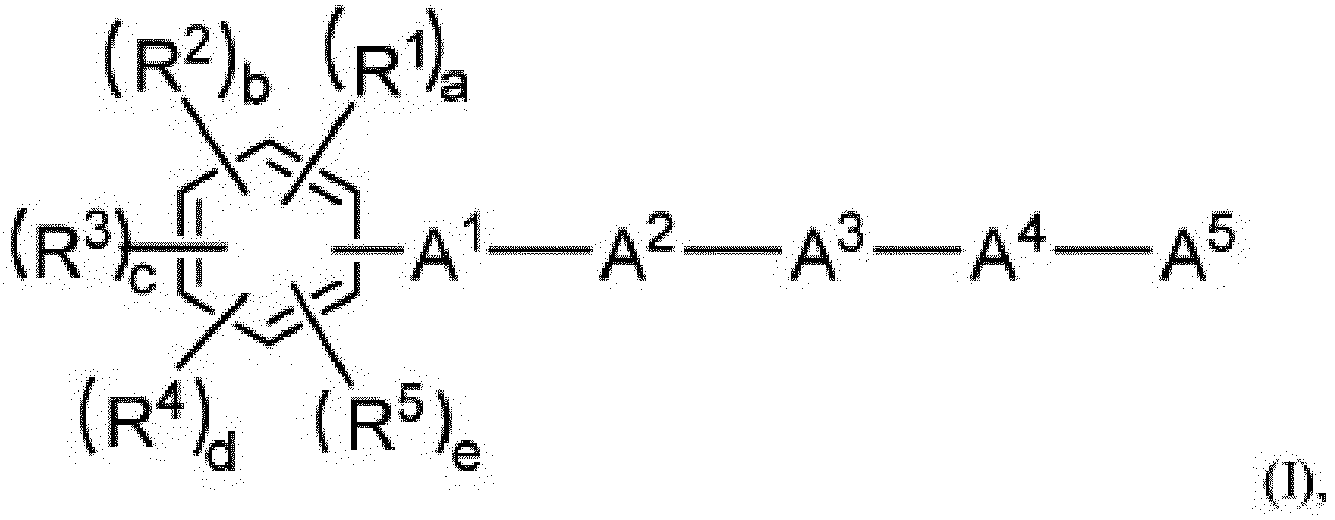 A1, A2, A3 et A4 étant indépendamment choisis parmi une simple liaison, un C6-30 arylène non substitué ou substitué et un C1-30 hétéroarylène non substitué ou substitué si au moins trois éléments directement reliés de celui-ci sont choisis pour être une simple liaison, ces éléments directement reliés forment ensemble une simple liaison ;A5 étant choisi parmi un groupe C6-40 aryle non substitué ou substitué et/ou parmi un groupe C2-40 hétéroaryle non substitué ou substitué,R1 à R5 étant indépendamment un groupe C6-30 aryle non substitué ou substitué, un groupe C2-30 hétéroaryle non substitué ou substitué ;dans le groupe substitué,au moins un hydrogène étant remplacé par(i) deutérium,(ii) un halogène,(iii) un groupe amino tertiaire en C2-60, l'atome d'azote du groupe amino tertiaire étant substitué par deux groupes hydrocarbyle en C1-30 indépendamment choisis ou l'atome d'azote du groupe amino tertiaire en C2-60 formant un groupe hétérocyclique en C1-30,(iv) un groupe C1-22 silyle,(v) un groupe C1-30 alkyle,(vi) un groupe C1-10 alkylsilyle,(vii) un groupe C6-22 arylsilyle,(viii) un groupe C3-30 cycloalkyle,(ix) un groupe C2-30 hétérocycloalkyle,(x) un groupe C6-30 aryle,(xi) un groupe C2-30 hétéroaryle,(xii) un groupe C1-20 alcoxy,(xiii) un groupe C1-30 perfluoro-hydrocarbyle,(xiv) un groupe C1-10 trifluoroalkyle, ou(xv) un groupe cyano ;a à e étant indépendamment un entier parmi 0 et 1 et 4 ≤ a+b+c+d+e ≤ 5;caractérisé en ce queb) la deuxième couche de transport d'électrons comprend un sel de métal alcalin ou un complexe organique de métal alcalin et un deuxième composé de matrice selon la formule (II) :
A-W (II),
A étant un dérivé d'acridine parmi une benzoacridine non substituée ou substituée et une dibenzoacridine non substituée ou substituée ; etW étant un groupe C16-48 aryle substitué ou non substitué comprenant 2 à 8 cycles aromatiques, ou un groupe C10-33 hétéroaryle substitué ou non substitué comprenant au moins 2 à 8 cycles aromatiques ; etles substituants étant choisis parmi deutérium, C1-12 alkyle et C1-12 alcoxy. - Dispositif électroluminescent organique selon la revendication 1, la première couche de transport d'électrons comprenant un premier composé de matrice d'électrons selon la formule (Ia)
 A2, A3 et A4 étant choisis pour être une simple liaison et formant ensemble une simple liaison ; Ar1 étant choisi parmi un C6-12 aryle et un C1-11 hétéroaryle ; etR1 à R5 étant indépendamment un groupe C6-30 aryle substitué ou non substitué, un groupe C2-30 hétéroaryle substitué ou non substitué ;a à e étant indépendamment un entier parmi 0 et 1 et 4 ≤ a+b+c+d+e ≤ 5;L étant une simple liaison, un groupe C6-30 arylène substitué ou non substitué, ou un groupe C2-30 hétéroarylène substitué ou non substitué ;ET étant un C6-40 aryle non substitué ou un C5-40 hétéroaryle non substitué ou un C6-40 aryle substitué ou un C5-40 hétéroaryle substitué ; et dans le groupe substitué,au moins un hydrogène étant remplacé par(i) deutérium,(ii) un halogène,(iii) un groupe amino tertiaire en C2-60, l'atome d'azote du groupe amino tertiaire en C2-60 étant substitué par deux groupes hydrocarbyle en C1-30 indépendamment choisis où l'atome d'azote du groupe amino tertiaire en C2-60 formant un groupe hétérocyclique en C1-30,(iv) un groupe C1-22 silyle,(v) un groupe C1-30 alkyle,(vi) un groupe C1-10 alkylsilyle,(vii) un groupe C6-22 arylsilyle,(viii) un groupe C3-30 cycloalkyle,(ix) un groupe C2-30 hétérocycloalkyle,(x) un groupe C6-30 aryle,(xi) un groupe C2-30 hétéroaryle,(xii) un groupe C1-20 alcoxy,(xiii) un groupe C1-30 perfluoro-hydrocarbyle,(xiv) un groupe C1-10 trifluoroalkyle, ou(xv) un groupe cyano.
 - Dispositif électroluminescent organique selon la revendication 1 ou 2, dans la formule (Ia)
R1 à R5 étant indépendamment un groupe C6-12 aryle substitué ou non substitué, un groupe C5-9 hétéroaryle substitué ou non substitué ;
a à e étant indépendamment un entier parmi 0 et 1 et 4 ≤ a+b+c+d+e ≤ 5;
L étant une simple liaison, un groupe C6-12 arylène substitué ou non substitué, ou un groupe C5-9 arylène substitué ou non substitué ;
ET étant un C6-18 aryle non substitué ou un C5-20 hétéroaryle non substitué ou un C6-18 aryle substitué ou un C5-20 hétéroaryle substitué ; et dans le groupe substitué,
au moins un hydrogène étant remplacé par(xvi) deutérium,(xvii) un groupe C1-12 alkyle,(xviii) un groupe C6-12 aryle,(xix) un groupe C5-9 hétéroaryle,(xx) un groupe C1-12 alcoxy. - Dispositif électroluminescent organique selon l'une quelconque des revendications précédentes 1 à 3, dans la formule (la), le groupe ET étant un groupe C2-30 hétéroaryle, préférablement ET étant choisi parmi les formules E1 et E2 :

- Dispositif électroluminescent organique selon l'une quelconque des revendications précédentes 1 à 4, dans la formule (II) :
A-W (II) ;
A étant choisi parmi le groupe de formule (IIIa) et (IIIb) :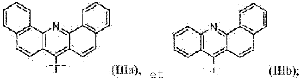 W étant un groupe C16-48 aryle substitué ou non substitué comprenant 2 à 8 cycles aromatiques, ou un groupe C10-33 hétéroaryle substitué ou non substitué comprenant au moins 2 à 8 cycles aromatiques ; etles substituants étant choisis parmi deutérium, C1-12 alkyle et C1-12 alcoxy.
 - Dispositif électroluminescent organique selon l'une quelconque des revendications précédentes 1 à 5, dans la formule (II) :A étant choisi parmi le groupe de formule (IIIa) et (IIIb) :
 W étant choisi parmi le groupe de formule IV :
-L-Ar2 (IV) ;
L étant choisi parmi phénylène, naphtylène et biphénylène ; etAr2 étant choisi parmi naphtyle, anthranyle, chrysényle, pyrényle, benzimidazolyle, pyridinyle, acridinyle, quinoléinyle, triazinyle substitué ou non substitué ; et les substituants étant choisis parmi deutérium, C1-12 alkyle et C1-12 alcoxy. - Dispositif électroluminescent organique selon l'une quelconque des revendications précédentes 1 à 6,- le sel de métal de métal alcalin étant choisi dans le groupe constitué par LiF, LiCl, LiBr et LiJ, et préférablement LiF ;- le complexe organique de métal alcalin étant choisi dans le groupe constitué par un quinoléinolate de lithium, un borate de lithium, un phénolate de lithium, un pyridinolate de lithium ou comprenant un lithium avec un ligand de type base de Schiff ;- préférablement, le complexe de quinoléinolate de lithium possédant la formule IV, V ou VI ;
 A1 à A6 étant identiques ou indépendamment choisis parmi CH, CR, N, O ;R étant identique ou indépendamment choisi parmi hydrogène, halogène, alkyle et aryle et hétéroaryle comportant 1 à 20 atomes de carbone ; et plus préférablement A1 à A6 étant CH ;- préférablement le ligand organique à base de borate étant un tétra(1H-pyrazol-1-yl)borate ;- préférablement, le phénolate étant un 2-(pyridin-2-yl)phénolate, un 2-(diphénylphosphoryl)phénolate, un imidazolphénolate, ou un 2-(pyridin-2-yl)phénolate et plus préférablement 2-(1-phényl-1H-benzo[d]imidazol-2-yl)phénolate ;- préférablement le pyridinolate étant un 2-(diphénylphosphoryl)pyridin-3-olate,- préférablement la base de Schiff de lithium possédant la structure 100, 101, 102 ou 103 :
- Dispositif électroluminescent organique selon l'une quelconque des revendications précédentes 1 à 7, le moment dipolaire du premier et/ou du deuxième composé de matrice de transport d'électrons étant ≥ 0 et ≤ 2,32 Debye, préférablement ≥ 0,2 et ≤ 2,2 Debye.
- Dispositif électroluminescent organique selon l'une quelconque des revendications précédentes 1 à 8, la première couche de transport d'électrons étant en contact en sandwich entre la couche d'émission et la deuxième couche de transport d'électrons, et la deuxième couche de transport d'électrons étant en contact en sandwich entre la première couche de transport d'électrons et la couche d'injection d'électrons.
- Dispositif électroluminescent organique selon l'une quelconque des revendications précédentes 1 à 9, le dispositif électroluminescent organique comprenant en outre une couche d'injection d'électrons (36) entre la deuxième couche de transport d'électrons et la cathode.
- Procédé de fabrication d'un dispositif électroluminescent organique (400) selon l'une quelconque des revendications 1 à 10,- sur une anode (150), une couche d'injection de trous (37), une couche de transport de trous (31), éventuellement une couche de blocage d'électrons (33), une couche d'émission (130), une première couche de transport d'électrons (135), une deuxième couche de transport d'électrons (34), une couche d'injection d'électrons (36), et une cathode (110), étant déposées dans cet ordre ; ou- les couches étant déposées dans l'autre sens, en partant de la cathode (110).
- Dispositif électronique comprenant au moins une diode luminescente organique (100), selon l'une quelconque des revendications précédentes 1 à 10, préférablement le dispositif électronique comprenant au moins une diode luminescente organique (100) selon l'une quelconque des revendications précédentes 1 à 10 étant un dispositif d'affichage.
Priority Applications (5)
| Application Number | Priority Date | Filing Date | Title |
|---|---|---|---|
| EP16195344.3A EP3312899B1 (fr) | 2016-10-24 | 2016-10-24 | Empilement de couches de transport d'électrons pour une diode électroluminescente organique |
| US15/788,431 US11011708B2 (en) | 2016-10-24 | 2017-10-19 | Electron transport layer stack for an organic light-emitting diode |
| JP2017202421A JP6985883B2 (ja) | 2016-10-24 | 2017-10-19 | 有機発光ダイオードのための電子伝達層の積層体 |
| KR1020170137278A KR102435687B1 (ko) | 2016-10-24 | 2017-10-23 | 유기 발광 다이오드용 전자 수송층 스택 |
| CN201711005583.7A CN107978684B (zh) | 2016-10-24 | 2017-10-24 | 用于有机发光二极管的电子传输层叠层 |
Applications Claiming Priority (1)
| Application Number | Priority Date | Filing Date | Title |
|---|---|---|---|
| EP16195344.3A EP3312899B1 (fr) | 2016-10-24 | 2016-10-24 | Empilement de couches de transport d'électrons pour une diode électroluminescente organique |
Publications (2)
| Publication Number | Publication Date |
|---|---|
| EP3312899A1 EP3312899A1 (fr) | 2018-04-25 |
| EP3312899B1 true EP3312899B1 (fr) | 2021-04-07 |
Family
ID=57208124
Family Applications (1)
| Application Number | Title | Priority Date | Filing Date |
|---|---|---|---|
| EP16195344.3A Active EP3312899B1 (fr) | 2016-10-24 | 2016-10-24 | Empilement de couches de transport d'électrons pour une diode électroluminescente organique |
Country Status (5)
| Country | Link |
|---|---|
| US (1) | US11011708B2 (fr) |
| EP (1) | EP3312899B1 (fr) |
| JP (1) | JP6985883B2 (fr) |
| KR (1) | KR102435687B1 (fr) |
| CN (1) | CN107978684B (fr) |
Families Citing this family (17)
| Publication number | Priority date | Publication date | Assignee | Title |
|---|---|---|---|---|
| US8774918B2 (en) | 2008-10-31 | 2014-07-08 | Medtronic, Inc. | Implantable medical device crosstalk evaluation and mitigation |
| CN106716665B9 (zh) * | 2014-10-27 | 2018-12-07 | 株式会社Lg化学 | 有机电致发光器件 |
| EP3312171B1 (fr) * | 2016-10-24 | 2019-07-31 | Novaled GmbH | Composé pour dispositif électronique et dispositif d'affichage et dispositif électronique |
| EP3556753B1 (fr) * | 2018-04-18 | 2023-10-11 | Novaled GmbH | Composé et couche semiconductrice organique, dispositif électronique organique, dispositif d'affichage et dispositif d'éclairage le comprenant |
| EP3653619A1 (fr) * | 2018-11-16 | 2020-05-20 | Novaled GmbH | Composé, dispositif électronique organique le comprenant, dispositif d'affichage et dispositif d'éclairage le comprenant |
| WO2020159128A1 (fr) * | 2019-01-28 | 2020-08-06 | 주식회사 엘지화학 | Dispositif électroluminescent organique |
| KR102778223B1 (ko) * | 2019-01-28 | 2025-03-10 | 주식회사 엘지화학 | 유기 발광 소자 |
| EP3694012B1 (fr) * | 2019-02-06 | 2026-02-11 | Novaled GmbH | Procédé de préparation d'une couche de semi-conducteur organique |
| EP3693352A1 (fr) * | 2019-02-06 | 2020-08-12 | Novaled GmbH | Composé et couche semiconductrice organique, dispositif électronique organique et dispositif d'affichage ou d'éclairage le comprenant |
| US20220216428A1 (en) * | 2019-04-15 | 2022-07-07 | Novaled Gmbh | See addendum |
| EP3730482A1 (fr) | 2019-04-24 | 2020-10-28 | Novaled GmbH | Composé et couche semi-conductrice organique comprenant celui-ci, dispositif électronique organique et afficheur ou dispositif d'éclairage comprenant celui-ci |
| EP3742513A1 (fr) | 2019-05-21 | 2020-11-25 | Novaled GmbH | Diode électroluminescente organique |
| CN110183381A (zh) * | 2019-06-28 | 2019-08-30 | 上海天马有机发光显示技术有限公司 | 一种化合物、oled显示面板以及电子设备 |
| EP3835295A1 (fr) * | 2019-12-10 | 2021-06-16 | Novaled GmbH | Composé acridine et couche semiconductrice organique, dispositif électronique organique et dispositif d'affichage le comprenant |
| EP3920249A1 (fr) | 2020-06-03 | 2021-12-08 | Novaled GmbH | Composé, intermédiaire du composé, procédé de préparation du composé, matériau semi-conducteur organique comprenant le composé, dispositif électronique organique comprenant le composé et dispositif d'affichage et dispositif d'éclairage comprenant le composé |
| EP3923363B1 (fr) * | 2020-06-12 | 2026-02-11 | Novaled GmbH | Diode électroluminescente organique et dispositif le comprenant |
| EP3923364B1 (fr) * | 2020-06-12 | 2025-09-17 | Novaled GmbH | Diode électroluminescente organique et dispositif le comprenant |
Family Cites Families (24)
| Publication number | Priority date | Publication date | Assignee | Title |
|---|---|---|---|---|
| US6800380B2 (en) | 1998-06-23 | 2004-10-05 | Nessdisplay Co., Ltd. | Organometallic luminescent materials and organic electroluminescent device containing same |
| JP3945123B2 (ja) | 2000-04-10 | 2007-07-18 | 三菱化学株式会社 | 有機電界発光素子 |
| AU2002317506A1 (en) * | 2001-07-11 | 2003-01-29 | Fuji Photo Film Co., Ltd. | Light-emitting device and aromatic compound |
| JP4003824B2 (ja) * | 2001-07-11 | 2007-11-07 | 富士フイルム株式会社 | 発光素子 |
| US20040209116A1 (en) * | 2003-04-21 | 2004-10-21 | Xiaofan Ren | Organic light emitting devices with wide gap host materials |
| JP2006279014A (ja) * | 2004-09-15 | 2006-10-12 | Fuji Photo Film Co Ltd | 有機電界発光素子 |
| US8049407B2 (en) * | 2004-09-15 | 2011-11-01 | Fujifilm Corporation | Organic electroluminescent element including blue phosphorescent luminescent material |
| EP1837927A1 (fr) | 2006-03-22 | 2007-09-26 | Novaled AG | Utilisation de radicaux hétérocycliques pour doper des semiconducteurs organiques |
| DE502006000749D1 (de) | 2006-03-21 | 2008-06-19 | Novaled Ag | Heterocyclisches Radikal oder Diradikal, deren Dimere, Oligomere, Polymere, Dispiroverbindungen und Polycyclen, deren Verwendung, organisches halbleitendes Material sowie elektronisches Bauelement |
| JP5683104B2 (ja) | 2006-03-21 | 2015-03-11 | ノヴァレッド・アクチエンゲゼルシャフト | ドープされた有機半導体材料の製造方法及びそのために用いられる配合物 |
| JP2008195623A (ja) | 2007-02-08 | 2008-08-28 | Chemiprokasei Kaisha Ltd | 新規な複素環含有ヒドロキシフェニル金属誘導体およびそれを用いた電子注入材料、電子輸送材料および有機エレクトロルミネッセンス素子 |
| JP5402639B2 (ja) * | 2007-10-26 | 2014-01-29 | コニカミノルタ株式会社 | 有機エレクトロルミネッセンス素子、表示装置及び照明装置 |
| EP2395571B1 (fr) | 2010-06-10 | 2013-12-04 | Novaled AG | Dispositif Électronique organique comprenant un matériau de semiconducteur organique |
| EP2724388B2 (fr) | 2011-06-22 | 2025-09-24 | Novaled GmbH | Dispositif électronique |
| TWI584513B (zh) * | 2011-11-30 | 2017-05-21 | 諾瓦發光二極體有限公司 | 顯示器 |
| WO2013079678A1 (fr) | 2011-11-30 | 2013-06-06 | Novaled Ag | Dispositif électronique organique |
| CN104067400B (zh) | 2011-11-30 | 2018-02-27 | 诺瓦尔德股份有限公司 | 有机电子器件 |
| EP2924029B1 (fr) * | 2013-03-15 | 2018-12-12 | Idemitsu Kosan Co., Ltd | Dérivé d'anthracène et élément électroluminescent organique l'utilisant |
| US9553274B2 (en) * | 2013-07-16 | 2017-01-24 | Universal Display Corporation | Organic electroluminescent materials and devices |
| KR20150014778A (ko) * | 2013-07-30 | 2015-02-09 | 삼성디스플레이 주식회사 | 유기 발광 소자 |
| KR20150096020A (ko) * | 2014-02-13 | 2015-08-24 | 삼성디스플레이 주식회사 | 유기 발광 소자 |
| EP3035400B1 (fr) * | 2014-12-17 | 2019-10-23 | Novaled GmbH | Diode électroluminescente organique comprenant des couches de transport d'électrons avec différents composés matriciels |
| KR101888934B1 (ko) * | 2015-04-24 | 2018-08-16 | 삼성에스디아이 주식회사 | 유기 광전자 소자용 화합물, 유기 광전자 소자 및 표시장치 |
| EP3182478B1 (fr) * | 2015-12-18 | 2018-11-28 | Novaled GmbH | Couche d'injection d'électrons pour une diode électroluminescente organique (oled) |
-
2016
- 2016-10-24 EP EP16195344.3A patent/EP3312899B1/fr active Active
-
2017
- 2017-10-19 US US15/788,431 patent/US11011708B2/en active Active
- 2017-10-19 JP JP2017202421A patent/JP6985883B2/ja active Active
- 2017-10-23 KR KR1020170137278A patent/KR102435687B1/ko active Active
- 2017-10-24 CN CN201711005583.7A patent/CN107978684B/zh active Active
Non-Patent Citations (1)
| Title |
|---|
| None * |
Also Published As
| Publication number | Publication date |
|---|---|
| CN107978684B (zh) | 2022-08-23 |
| JP6985883B2 (ja) | 2021-12-22 |
| JP2018117112A (ja) | 2018-07-26 |
| KR20180044821A (ko) | 2018-05-03 |
| CN107978684A (zh) | 2018-05-01 |
| EP3312899A1 (fr) | 2018-04-25 |
| KR102435687B1 (ko) | 2022-08-23 |
| US20180114920A1 (en) | 2018-04-26 |
| US11011708B2 (en) | 2021-05-18 |
Similar Documents
| Publication | Publication Date | Title |
|---|---|---|
| EP3312899B1 (fr) | Empilement de couches de transport d'électrons pour une diode électroluminescente organique | |
| KR102677419B1 (ko) | 정공 주입층 및 영가 금속을 함유하는 전자 주입층을 포함하는 유기 전계발광 장치 | |
| EP3312895B1 (fr) | Matériau organique semi-conducteur comprenant un dopant-n électrique et une matrice de transport d'électrons et dispositif électronique comprenant le matériau semi-conducteur | |
| EP3689867B1 (fr) | Composition, couche semi-conductrice organique et dispositif électronique | |
| EP3898606B1 (fr) | Composé et couche semiconductrice organique, dispositif électronique organique et dispositif d'affichage le comprenant | |
| US11524952B2 (en) | Compound and organic semiconducting layer, organic electronic device, display device and lighting device comprising the same | |
| EP3503240B1 (fr) | Couche à semi-conducteur organique | |
| US11145826B2 (en) | Compound for electronic device and electronic device and display device | |
| KR102583049B1 (ko) | 전자 장치 및 디스플레이 장치에 사용하기 위한 아크리딘 화합물 | |
| KR102628725B1 (ko) | 트리아진기, 플루오렌기 및 헤테로-플루오렌기를 포함하는 화합물 | |
| EP3527557A1 (fr) | Composés n-hétéroarylène | |
| KR102639012B1 (ko) | 트리아진기, 플루오렌기 및 아릴기를 포함하는 화합물 | |
| EP3693352A1 (fr) | Composé et couche semiconductrice organique, dispositif électronique organique et dispositif d'affichage ou d'éclairage le comprenant | |
| KR102685005B1 (ko) | 트리아진기, 플루오렌기 및 아릴기를 포함하는 화합물 |
Legal Events
| Date | Code | Title | Description |
|---|---|---|---|
| PUAI | Public reference made under article 153(3) epc to a published international application that has entered the european phase |
Free format text: ORIGINAL CODE: 0009012 |
|
| STAA | Information on the status of an ep patent application or granted ep patent |
Free format text: STATUS: THE APPLICATION HAS BEEN PUBLISHED |
|
| AK | Designated contracting states |
Kind code of ref document: A1 Designated state(s): AL AT BE BG CH CY CZ DE DK EE ES FI FR GB GR HR HU IE IS IT LI LT LU LV MC MK MT NL NO PL PT RO RS SE SI SK SM TR |
|
| AX | Request for extension of the european patent |
Extension state: BA ME |
|
| STAA | Information on the status of an ep patent application or granted ep patent |
Free format text: STATUS: REQUEST FOR EXAMINATION WAS MADE |
|
| 17P | Request for examination filed |
Effective date: 20181024 |
|
| RBV | Designated contracting states (corrected) |
Designated state(s): AL AT BE BG CH CY CZ DE DK EE ES FI FR GB GR HR HU IE IS IT LI LT LU LV MC MK MT NL NO PL PT RO RS SE SI SK SM TR |
|
| RAP1 | Party data changed (applicant data changed or rights of an application transferred) |
Owner name: SAMSUNG SDI CO., LTD. Owner name: NOVALED GMBH |
|
| GRAJ | Information related to disapproval of communication of intention to grant by the applicant or resumption of examination proceedings by the epo deleted |
Free format text: ORIGINAL CODE: EPIDOSDIGR1 |
|
| STAA | Information on the status of an ep patent application or granted ep patent |
Free format text: STATUS: GRANT OF PATENT IS INTENDED |
|
| GRAP | Despatch of communication of intention to grant a patent |
Free format text: ORIGINAL CODE: EPIDOSNIGR1 |
|
| INTG | Intention to grant announced |
Effective date: 20201111 |
|
| GRAS | Grant fee paid |
Free format text: ORIGINAL CODE: EPIDOSNIGR3 |
|
| GRAA | (expected) grant |
Free format text: ORIGINAL CODE: 0009210 |
|
| STAA | Information on the status of an ep patent application or granted ep patent |
Free format text: STATUS: THE PATENT HAS BEEN GRANTED |
|
| AK | Designated contracting states |
Kind code of ref document: B1 Designated state(s): AL AT BE BG CH CY CZ DE DK EE ES FI FR GB GR HR HU IE IS IT LI LT LU LV MC MK MT NL NO PL PT RO RS SE SI SK SM TR |
|
| REG | Reference to a national code |
Ref country code: GB Ref legal event code: FG4D |
|
| REG | Reference to a national code |
Ref country code: AT Ref legal event code: REF Ref document number: 1380824 Country of ref document: AT Kind code of ref document: T Effective date: 20210415 Ref country code: CH Ref legal event code: EP |
|
| REG | Reference to a national code |
Ref country code: DE Ref legal event code: R096 Ref document number: 602016055555 Country of ref document: DE |
|
| REG | Reference to a national code |
Ref country code: IE Ref legal event code: FG4D |
|
| REG | Reference to a national code |
Ref country code: LT Ref legal event code: MG9D |
|
| REG | Reference to a national code |
Ref country code: NL Ref legal event code: MP Effective date: 20210407 Ref country code: AT Ref legal event code: MK05 Ref document number: 1380824 Country of ref document: AT Kind code of ref document: T Effective date: 20210407 |
|
| PG25 | Lapsed in a contracting state [announced via postgrant information from national office to epo] |
Ref country code: HR Free format text: LAPSE BECAUSE OF FAILURE TO SUBMIT A TRANSLATION OF THE DESCRIPTION OR TO PAY THE FEE WITHIN THE PRESCRIBED TIME-LIMIT Effective date: 20210407 Ref country code: BG Free format text: LAPSE BECAUSE OF FAILURE TO SUBMIT A TRANSLATION OF THE DESCRIPTION OR TO PAY THE FEE WITHIN THE PRESCRIBED TIME-LIMIT Effective date: 20210707 Ref country code: AT Free format text: LAPSE BECAUSE OF FAILURE TO SUBMIT A TRANSLATION OF THE DESCRIPTION OR TO PAY THE FEE WITHIN THE PRESCRIBED TIME-LIMIT Effective date: 20210407 Ref country code: FI Free format text: LAPSE BECAUSE OF FAILURE TO SUBMIT A TRANSLATION OF THE DESCRIPTION OR TO PAY THE FEE WITHIN THE PRESCRIBED TIME-LIMIT Effective date: 20210407 Ref country code: LT Free format text: LAPSE BECAUSE OF FAILURE TO SUBMIT A TRANSLATION OF THE DESCRIPTION OR TO PAY THE FEE WITHIN THE PRESCRIBED TIME-LIMIT Effective date: 20210407 Ref country code: NL Free format text: LAPSE BECAUSE OF FAILURE TO SUBMIT A TRANSLATION OF THE DESCRIPTION OR TO PAY THE FEE WITHIN THE PRESCRIBED TIME-LIMIT Effective date: 20210407 |
|
| PG25 | Lapsed in a contracting state [announced via postgrant information from national office to epo] |
Ref country code: NO Free format text: LAPSE BECAUSE OF FAILURE TO SUBMIT A TRANSLATION OF THE DESCRIPTION OR TO PAY THE FEE WITHIN THE PRESCRIBED TIME-LIMIT Effective date: 20210707 Ref country code: PT Free format text: LAPSE BECAUSE OF FAILURE TO SUBMIT A TRANSLATION OF THE DESCRIPTION OR TO PAY THE FEE WITHIN THE PRESCRIBED TIME-LIMIT Effective date: 20210809 Ref country code: PL Free format text: LAPSE BECAUSE OF FAILURE TO SUBMIT A TRANSLATION OF THE DESCRIPTION OR TO PAY THE FEE WITHIN THE PRESCRIBED TIME-LIMIT Effective date: 20210407 Ref country code: RS Free format text: LAPSE BECAUSE OF FAILURE TO SUBMIT A TRANSLATION OF THE DESCRIPTION OR TO PAY THE FEE WITHIN THE PRESCRIBED TIME-LIMIT Effective date: 20210407 Ref country code: SE Free format text: LAPSE BECAUSE OF FAILURE TO SUBMIT A TRANSLATION OF THE DESCRIPTION OR TO PAY THE FEE WITHIN THE PRESCRIBED TIME-LIMIT Effective date: 20210407 Ref country code: IS Free format text: LAPSE BECAUSE OF FAILURE TO SUBMIT A TRANSLATION OF THE DESCRIPTION OR TO PAY THE FEE WITHIN THE PRESCRIBED TIME-LIMIT Effective date: 20210807 Ref country code: GR Free format text: LAPSE BECAUSE OF FAILURE TO SUBMIT A TRANSLATION OF THE DESCRIPTION OR TO PAY THE FEE WITHIN THE PRESCRIBED TIME-LIMIT Effective date: 20210708 Ref country code: LV Free format text: LAPSE BECAUSE OF FAILURE TO SUBMIT A TRANSLATION OF THE DESCRIPTION OR TO PAY THE FEE WITHIN THE PRESCRIBED TIME-LIMIT Effective date: 20210407 |
|
| REG | Reference to a national code |
Ref country code: DE Ref legal event code: R097 Ref document number: 602016055555 Country of ref document: DE |
|
| PG25 | Lapsed in a contracting state [announced via postgrant information from national office to epo] |
Ref country code: DK Free format text: LAPSE BECAUSE OF FAILURE TO SUBMIT A TRANSLATION OF THE DESCRIPTION OR TO PAY THE FEE WITHIN THE PRESCRIBED TIME-LIMIT Effective date: 20210407 Ref country code: CZ Free format text: LAPSE BECAUSE OF FAILURE TO SUBMIT A TRANSLATION OF THE DESCRIPTION OR TO PAY THE FEE WITHIN THE PRESCRIBED TIME-LIMIT Effective date: 20210407 Ref country code: EE Free format text: LAPSE BECAUSE OF FAILURE TO SUBMIT A TRANSLATION OF THE DESCRIPTION OR TO PAY THE FEE WITHIN THE PRESCRIBED TIME-LIMIT Effective date: 20210407 Ref country code: SK Free format text: LAPSE BECAUSE OF FAILURE TO SUBMIT A TRANSLATION OF THE DESCRIPTION OR TO PAY THE FEE WITHIN THE PRESCRIBED TIME-LIMIT Effective date: 20210407 Ref country code: SM Free format text: LAPSE BECAUSE OF FAILURE TO SUBMIT A TRANSLATION OF THE DESCRIPTION OR TO PAY THE FEE WITHIN THE PRESCRIBED TIME-LIMIT Effective date: 20210407 Ref country code: RO Free format text: LAPSE BECAUSE OF FAILURE TO SUBMIT A TRANSLATION OF THE DESCRIPTION OR TO PAY THE FEE WITHIN THE PRESCRIBED TIME-LIMIT Effective date: 20210407 Ref country code: ES Free format text: LAPSE BECAUSE OF FAILURE TO SUBMIT A TRANSLATION OF THE DESCRIPTION OR TO PAY THE FEE WITHIN THE PRESCRIBED TIME-LIMIT Effective date: 20210407 |
|
| PLBE | No opposition filed within time limit |
Free format text: ORIGINAL CODE: 0009261 |
|
| STAA | Information on the status of an ep patent application or granted ep patent |
Free format text: STATUS: NO OPPOSITION FILED WITHIN TIME LIMIT |
|
| 26N | No opposition filed |
Effective date: 20220110 |
|
| REG | Reference to a national code |
Ref country code: CH Ref legal event code: PL |
|
| PG25 | Lapsed in a contracting state [announced via postgrant information from national office to epo] |
Ref country code: IS Free format text: LAPSE BECAUSE OF FAILURE TO SUBMIT A TRANSLATION OF THE DESCRIPTION OR TO PAY THE FEE WITHIN THE PRESCRIBED TIME-LIMIT Effective date: 20210807 Ref country code: AL Free format text: LAPSE BECAUSE OF FAILURE TO SUBMIT A TRANSLATION OF THE DESCRIPTION OR TO PAY THE FEE WITHIN THE PRESCRIBED TIME-LIMIT Effective date: 20210407 |
|
| REG | Reference to a national code |
Ref country code: BE Ref legal event code: MM Effective date: 20211031 |
|
| GBPC | Gb: european patent ceased through non-payment of renewal fee |
Effective date: 20211024 |
|
| PG25 | Lapsed in a contracting state [announced via postgrant information from national office to epo] |
Ref country code: MC Free format text: LAPSE BECAUSE OF FAILURE TO SUBMIT A TRANSLATION OF THE DESCRIPTION OR TO PAY THE FEE WITHIN THE PRESCRIBED TIME-LIMIT Effective date: 20210407 |
|
| PG25 | Lapsed in a contracting state [announced via postgrant information from national office to epo] |
Ref country code: LU Free format text: LAPSE BECAUSE OF NON-PAYMENT OF DUE FEES Effective date: 20211024 Ref country code: IT Free format text: LAPSE BECAUSE OF FAILURE TO SUBMIT A TRANSLATION OF THE DESCRIPTION OR TO PAY THE FEE WITHIN THE PRESCRIBED TIME-LIMIT Effective date: 20210407 Ref country code: GB Free format text: LAPSE BECAUSE OF NON-PAYMENT OF DUE FEES Effective date: 20211024 Ref country code: BE Free format text: LAPSE BECAUSE OF NON-PAYMENT OF DUE FEES Effective date: 20211031 |
|
| PG25 | Lapsed in a contracting state [announced via postgrant information from national office to epo] |
Ref country code: LI Free format text: LAPSE BECAUSE OF NON-PAYMENT OF DUE FEES Effective date: 20211031 Ref country code: CH Free format text: LAPSE BECAUSE OF NON-PAYMENT OF DUE FEES Effective date: 20211031 |
|
| PG25 | Lapsed in a contracting state [announced via postgrant information from national office to epo] |
Ref country code: FR Free format text: LAPSE BECAUSE OF NON-PAYMENT OF DUE FEES Effective date: 20211031 |
|
| PG25 | Lapsed in a contracting state [announced via postgrant information from national office to epo] |
Ref country code: IE Free format text: LAPSE BECAUSE OF NON-PAYMENT OF DUE FEES Effective date: 20211024 |
|
| REG | Reference to a national code |
Ref country code: DE Ref legal event code: R079 Ref document number: 602016055555 Country of ref document: DE Free format text: PREVIOUS MAIN CLASS: H01L0051520000 Ipc: H10K0050800000 |
|
| PG25 | Lapsed in a contracting state [announced via postgrant information from national office to epo] |
Ref country code: HU Free format text: LAPSE BECAUSE OF FAILURE TO SUBMIT A TRANSLATION OF THE DESCRIPTION OR TO PAY THE FEE WITHIN THE PRESCRIBED TIME-LIMIT; INVALID AB INITIO Effective date: 20161024 |
|
| PG25 | Lapsed in a contracting state [announced via postgrant information from national office to epo] |
Ref country code: CY Free format text: LAPSE BECAUSE OF FAILURE TO SUBMIT A TRANSLATION OF THE DESCRIPTION OR TO PAY THE FEE WITHIN THE PRESCRIBED TIME-LIMIT Effective date: 20210407 |
|
| P01 | Opt-out of the competence of the unified patent court (upc) registered |
Effective date: 20230526 |
|
| PG25 | Lapsed in a contracting state [announced via postgrant information from national office to epo] |
Ref country code: MK Free format text: LAPSE BECAUSE OF FAILURE TO SUBMIT A TRANSLATION OF THE DESCRIPTION OR TO PAY THE FEE WITHIN THE PRESCRIBED TIME-LIMIT Effective date: 20210407 |
|
| PG25 | Lapsed in a contracting state [announced via postgrant information from national office to epo] |
Ref country code: TR Free format text: LAPSE BECAUSE OF FAILURE TO SUBMIT A TRANSLATION OF THE DESCRIPTION OR TO PAY THE FEE WITHIN THE PRESCRIBED TIME-LIMIT Effective date: 20210407 |
|
| PG25 | Lapsed in a contracting state [announced via postgrant information from national office to epo] |
Ref country code: MT Free format text: LAPSE BECAUSE OF FAILURE TO SUBMIT A TRANSLATION OF THE DESCRIPTION OR TO PAY THE FEE WITHIN THE PRESCRIBED TIME-LIMIT Effective date: 20210407 |
|
| PGFP | Annual fee paid to national office [announced via postgrant information from national office to epo] |
Ref country code: DE Payment date: 20250827 Year of fee payment: 10 |