EP3314635B1 - Procédé pour la formation de contacts ohmiques à des semi-conducteurs au moyen de métaux quantifiés - Google Patents
Procédé pour la formation de contacts ohmiques à des semi-conducteurs au moyen de métaux quantifiés Download PDFInfo
- Publication number
- EP3314635B1 EP3314635B1 EP15897299.2A EP15897299A EP3314635B1 EP 3314635 B1 EP3314635 B1 EP 3314635B1 EP 15897299 A EP15897299 A EP 15897299A EP 3314635 B1 EP3314635 B1 EP 3314635B1
- Authority
- EP
- European Patent Office
- Prior art keywords
- metal
- contact
- semiconductor material
- contact area
- drain
- Prior art date
- Legal status (The legal status is an assumption and is not a legal conclusion. Google has not performed a legal analysis and makes no representation as to the accuracy of the status listed.)
- Active
Links
Images



Classifications
-
- H—ELECTRICITY
- H10—SEMICONDUCTOR DEVICES; ELECTRIC SOLID-STATE DEVICES NOT OTHERWISE PROVIDED FOR
- H10D—INORGANIC ELECTRIC SEMICONDUCTOR DEVICES
- H10D64/00—Electrodes of devices having potential barriers
- H10D64/60—Electrodes characterised by their materials
- H10D64/62—Electrodes ohmically coupled to a semiconductor
-
- H—ELECTRICITY
- H10—SEMICONDUCTOR DEVICES; ELECTRIC SOLID-STATE DEVICES NOT OTHERWISE PROVIDED FOR
- H10D—INORGANIC ELECTRIC SEMICONDUCTOR DEVICES
- H10D30/00—Field-effect transistors [FET]
- H10D30/01—Manufacture or treatment
- H10D30/021—Manufacture or treatment of FETs having insulated gates [IGFET]
- H10D30/027—Manufacture or treatment of FETs having insulated gates [IGFET] of lateral single-gate IGFETs
-
- H—ELECTRICITY
- H10—SEMICONDUCTOR DEVICES; ELECTRIC SOLID-STATE DEVICES NOT OTHERWISE PROVIDED FOR
- H10D—INORGANIC ELECTRIC SEMICONDUCTOR DEVICES
- H10D30/00—Field-effect transistors [FET]
- H10D30/60—Insulated-gate field-effect transistors [IGFET]
-
- H—ELECTRICITY
- H10—SEMICONDUCTOR DEVICES; ELECTRIC SOLID-STATE DEVICES NOT OTHERWISE PROVIDED FOR
- H10D—INORGANIC ELECTRIC SEMICONDUCTOR DEVICES
- H10D62/00—Semiconductor bodies, or regions thereof, of devices having potential barriers
- H10D62/10—Shapes, relative sizes or dispositions of the regions of the semiconductor bodies; Shapes of the semiconductor bodies
- H10D62/13—Semiconductor regions connected to electrodes carrying current to be rectified, amplified or switched, e.g. source or drain regions
- H10D62/149—Source or drain regions of field-effect devices
- H10D62/151—Source or drain regions of field-effect devices of IGFETs
-
- H—ELECTRICITY
- H10—SEMICONDUCTOR DEVICES; ELECTRIC SOLID-STATE DEVICES NOT OTHERWISE PROVIDED FOR
- H10D—INORGANIC ELECTRIC SEMICONDUCTOR DEVICES
- H10D62/00—Semiconductor bodies, or regions thereof, of devices having potential barriers
- H10D62/80—Semiconductor bodies, or regions thereof, of devices having potential barriers characterised by the materials
- H10D62/81—Semiconductor bodies, or regions thereof, of devices having potential barriers characterised by the materials of structures exhibiting quantum-confinement effects, e.g. single quantum wells; of structures having periodic or quasi-periodic potential variation
- H10D62/812—Single quantum well structures
-
- H—ELECTRICITY
- H10—SEMICONDUCTOR DEVICES; ELECTRIC SOLID-STATE DEVICES NOT OTHERWISE PROVIDED FOR
- H10D—INORGANIC ELECTRIC SEMICONDUCTOR DEVICES
- H10D64/00—Electrodes of devices having potential barriers
- H10D64/20—Electrodes characterised by their shapes, relative sizes or dispositions
- H10D64/23—Electrodes carrying the current to be rectified, amplified, oscillated or switched, e.g. sources, drains, anodes or cathodes
- H10D64/251—Source or drain electrodes for field-effect devices
- H10D64/258—Source or drain electrodes for field-effect devices characterised by the relative positions of the source or drain electrodes with respect to the gate electrode
- H10D64/259—Source or drain electrodes being self-aligned with the gate electrode and having bottom surfaces higher than the interface between the channel and the gate dielectric
-
- H—ELECTRICITY
- H10—SEMICONDUCTOR DEVICES; ELECTRIC SOLID-STATE DEVICES NOT OTHERWISE PROVIDED FOR
- H10P—GENERIC PROCESSES OR APPARATUS FOR THE MANUFACTURE OR TREATMENT OF DEVICES COVERED BY CLASS H10
- H10P14/00—Formation of materials, e.g. in the shape of layers or pillars
- H10P14/40—Formation of materials, e.g. in the shape of layers or pillars of conductive or resistive materials
- H10P14/418—Formation of materials, e.g. in the shape of layers or pillars of conductive or resistive materials the conductive layers comprising transition metals
-
- H—ELECTRICITY
- H10—SEMICONDUCTOR DEVICES; ELECTRIC SOLID-STATE DEVICES NOT OTHERWISE PROVIDED FOR
- H10W—GENERIC PACKAGES, INTERCONNECTIONS, CONNECTORS OR OTHER CONSTRUCTIONAL DETAILS OF DEVICES COVERED BY CLASS H10
- H10W20/00—Interconnections in chips, wafers or substrates
- H10W20/01—Manufacture or treatment
- H10W20/031—Manufacture or treatment of conductive parts of the interconnections
- H10W20/056—Manufacture or treatment of conductive parts of the interconnections by filling conductive material into holes, grooves or trenches
-
- H—ELECTRICITY
- H10—SEMICONDUCTOR DEVICES; ELECTRIC SOLID-STATE DEVICES NOT OTHERWISE PROVIDED FOR
- H10W—GENERIC PACKAGES, INTERCONNECTIONS, CONNECTORS OR OTHER CONSTRUCTIONAL DETAILS OF DEVICES COVERED BY CLASS H10
- H10W20/00—Interconnections in chips, wafers or substrates
- H10W20/01—Manufacture or treatment
- H10W20/071—Manufacture or treatment of dielectric parts thereof
- H10W20/081—Manufacture or treatment of dielectric parts thereof by forming openings in the dielectric parts
-
- H—ELECTRICITY
- H10—SEMICONDUCTOR DEVICES; ELECTRIC SOLID-STATE DEVICES NOT OTHERWISE PROVIDED FOR
- H10P—GENERIC PROCESSES OR APPARATUS FOR THE MANUFACTURE OR TREATMENT OF DEVICES COVERED BY CLASS H10
- H10P14/00—Formation of materials, e.g. in the shape of layers or pillars
- H10P14/40—Formation of materials, e.g. in the shape of layers or pillars of conductive or resistive materials
- H10P14/42—Formation of materials, e.g. in the shape of layers or pillars of conductive or resistive materials using a gas or vapour
- H10P14/43—Chemical deposition, e.g. chemical vapour deposition [CVD]
-
- H—ELECTRICITY
- H10—SEMICONDUCTOR DEVICES; ELECTRIC SOLID-STATE DEVICES NOT OTHERWISE PROVIDED FOR
- H10W—GENERIC PACKAGES, INTERCONNECTIONS, CONNECTORS OR OTHER CONSTRUCTIONAL DETAILS OF DEVICES COVERED BY CLASS H10
- H10W70/00—Package substrates; Interposers; Redistribution layers [RDL]
- H10W70/60—Insulating or insulated package substrates; Interposers; Redistribution layers
- H10W70/62—Insulating or insulated package substrates; Interposers; Redistribution layers characterised by their interconnections
- H10W70/63—Vias, e.g. via plugs
- H10W70/635—Through-vias
-
- H—ELECTRICITY
- H10—SEMICONDUCTOR DEVICES; ELECTRIC SOLID-STATE DEVICES NOT OTHERWISE PROVIDED FOR
- H10W—GENERIC PACKAGES, INTERCONNECTIONS, CONNECTORS OR OTHER CONSTRUCTIONAL DETAILS OF DEVICES COVERED BY CLASS H10
- H10W70/00—Package substrates; Interposers; Redistribution layers [RDL]
- H10W70/60—Insulating or insulated package substrates; Interposers; Redistribution layers
- H10W70/62—Insulating or insulated package substrates; Interposers; Redistribution layers characterised by their interconnections
- H10W70/65—Shapes or dispositions of interconnections
Definitions
- Integrated circuit devices often employ metal to semiconductor contacts.
- One example is a contact to a junction region (source or drain region) of a transistor device.
- Document EP 2701196 discloses a semiconductor device which includes a semiconductor substrate having a channel region therein, a gate structure above the channel region, and source and drain regions on opposite sides of the gate structure.
- Document JP 2006024809 discloses a semiconductor apparatus having a structure capable of supressing a leakage current entailed by a pn-junctinon leakage, and to provide its manufacturing method.
- Document EP 0 838 862 A1 discloses a semiconductor device with trench isolation including silicide layers covering the side wall portions of a device region exposed in contact holes.
- a contact resistance between a metal and a semiconductor material is reduced by grading a metal/semiconductor material interface to smooth out a band discontinuity.
- the grading is achieved by confining (e.g., quantizing) a low density of states metal with the metal being more confined (e.g., more quantized) toward the semiconductor.
- Figure 1 shows a cross-sectional side view of an embodiment of a transistor device having metal contacts formed to junction regions of the device.
- device structure 100 includes substrate 110 of a semiconductor material such as silicon, silicon germanium, germanium, a III-V, or a II-VI compound semiconductor. Disposed on substrate 110 is a transistor device including junction region 120 (e.g., a source), junction region 130 (e.g., a drain), channel 140 between the source and drain, gate dielectric 145 and gate electrode 150 on channel 140.
- Dielectric material 180 surrounds components of the device structure.
- junction region 120 and junction region 130 are a semiconductor material such as a doped silicon, silicon germanium, germanium, a III-V, or a II-VI compound semiconductor.
- junction region 120 and junction region 130 are each, for example, p + silicon germanium or p + silicon.
- Figure 1 shows metal contacts to each of junction region 120 and junction region 130.
- a material of metal contact 160 and metal contact 170 to the respective junction regions is a low density of states metal.
- Low density of states metals according to the invention are antimony (Sb), bismuth (Bi), tin (Sn) and their alloys. These metals may be deposited by physical line of sight methods such as evaporation or sputtering or chemical means such as chemical vapor deposition (CVD) and atomical layer deposition (ALD).
- Chemical thin film deposition techniques include but are not limited to the use of a volatile metal chloride such as SbCl 3 or SnCl4 as one precursor along with a coreactant such as hydrogen plasma or a homometal silyl coreactant such as Sb(SiR 3 ) 3 or Sn(SiR 3 ) 4 or Sn(SiR 3 ) 2 , where R is an organic substituent including but not limited to methyl, ethyl, isopropyl, butyl or phenyl.
- the metal may or may not be annealed under an inert or reducing atmosphere such as one containing hydrogen.
- Figure 1 shows the interface between the metal contact and semiconductor material of the junction (contact 160/junction region 120 and contact 170/junction region 130) as graded in the sense that the metal is increasingly confined by semiconductor material.
- Figure 1 shows the metal to semiconductor material interface having a profile such that, proceeding in a direction toward substrate 110, the contact area between semiconductor material and metal taken through a horizontal cross-section of the interface (as viewed) gets progressively smaller. Such confinement tends to quantize a metal of the contact.
- Figure 2 shows a portion of the transistor device and a corresponding bandgap.
- Figure 2 shows that the grading of the metal/semiconductor material interface to progressively confine (e.g., quantize) the metal results in a grading of the band discontinuity.
- Figure 2 illustrates a barrier height at a first position (position 1) where a cross-sectional contact area between the metal and semiconductor material is dominated by metal material (least confined metal state) has a barrier height between a valence band and the metal work function.
- the resistance is reduced as e ⁇ B1 •k + e ⁇ B2 •k + e ⁇ B3 •k + e ⁇ B4 •k is less than e ⁇ PB 0 k.
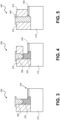
- Figure 3 shows a cross-sectional side view of a portion of another embodiment of a transistor device, not forming part of the invention.
- Device 200 includes junction region 220 (e.g., a source or drain) at channel 240 on substrate 210 with metal contact 260 to junction region 220.
- Figure 3 shows an interface having a conical shape. Either the graded interface ( Figure 1 ) or the conical interface of Figure 3 may be formed by an etching process into the junction region material followed by metal deposition. In another embodiment, such a conical or stepped etch profile need not be precise (e.g., because of an etch recipe or tool property) but is suitable to the extent that the low density of states metal is confined (e.g., quantized) in a contact with a profile such as contact 260 or contact 160.
- Figure 4 shows a cross-sectional side view of a portion of another embodiment of a transistor device, not forming part of the invention.
- Figure 4 shows transistor device 300 including junction region 320 (e.g., a source or drain) and channel 340 on substrate 310.
- Figure 4 also shows contact 360 to junction region 320.
- contact 360 of, for example, a low density of states metal is confined by dielectric material 370.
- a dielectric material such as deposited silicon dioxide is a high bandgap material which as it confines the metal will reflect a band structure similar to that shown in Figure 2
- a cross-sectional area of metal contact 360 is reduced, in this embodiment, in a conical way in a direction toward junction region 320.
- the confinement of metal contact 360 in a direction toward semiconductor material 320 can have other profiles including a step profile for a regular profile that similarly confines (e.g., quantizes) a metal material.
- Figure 5 shows another embodiment of a portion of a transistor device, not forming part of the invention.
- Device 400 includes channel 440 formed on substrate 410 and metal contact 460 directly contacted to channel 440.
- a junction region (source or drain) of, for example, semiconductor material is removed and metal directly contacts channel 440 of the transistor device.
- contact 460 is defined through dielectric layer 470.
- the metal As the metal contacts channel 440, the metal is confined by dielectric layer 470 at channel 440.
- Each of dielectric layer 470 and a low doped semiconductor material for channel 440 is a high bandgap material. The high bandgap will tend to increase the barrier. Thus, increasing a confinement of the metal, in this case, in a direction toward channel 440 will have a tendency to smooth out for junction and reduce a contact resistance.
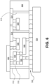
- Interposer 500 is an intervening substrate used to bridge first substrate 502 to second substrate 504.
- First substrate 502 may be, for instance, an integrated circuit die.
- Second substrate 504 may be, for instance, a memory module, a computer motherboard, or another integrated circuit die.
- the purpose of interposer 500 is to spread a connection to a wider pitch or to reroute a connection to a different connection.
- interposer 500 may couple an integrated circuit die to ball grid array (BGA) 506 that can subsequently be coupled to second substrate 504.
- BGA ball grid array
- first and second substrates 502/504 are attached to opposing sides of interposer 500.
- the first and second substrates 502/504 are attached to the same side of interposer 500.
- three or more substrates are interconnected by way of interposer 500.
- Interposer 500 may be formed of an epoxy resin, a fiberglass-reinforced epoxy resin, a ceramic material, or a polymer material such as polyimide.
- the interposer may be formed of alternate rigid or flexible materials that may include the same materials described above for use in a semiconductor substrate, such as silicon, germanium, and other group III-V and group IV materials.
- the interposer may include metal interconnects 508 and vias 510, including but not limited to through-silicon vias (TSVs) 512.
- the interposer 500 may further include embedded devices 514, including both passive and active devices. Such devices include, but are not limited to, capacitors, decoupling capacitors, resistors, inductors, fuses, diodes, transformers, sensors, and electrostatic discharge (ESD) devices. More complex devices such as radio-frequency (RF) devices, power amplifiers, power management devices, antennas, arrays, sensors, and MEMS devices may also be formed on interposer 500.
- RF radio-frequency
- apparatuses or processes disclosed herein may be used in the fabrication of interposer 500.
- FIG. 7 illustrates a computing device in accordance with one embodiment.
- Computing device 600 may include a number of components. In one embodiment, these components are attached to one or more motherboards. In an alternate embodiment, these components are fabricated onto a single system-on-a-chip (SoC) die rather than a motherboard.
- the components in computing device 600 include, but are not limited to, integrated circuit die 602 and at least one communication chip 608.
- the communication chip 608 is fabricated as part of integrated circuit die 602.
- Integrated circuit die 602 may include CPU 604 as well as on-die memory 606, often used as cache memory, that can be provided by technologies such as embedded DRAM (eDRAM) or spin-transfer torque memory (STTM or STTM-RAM).
- eDRAM embedded DRAM
- STTM spin-transfer torque memory
- Computing device 600 may include other components that may or may not be physically and electrically coupled to the motherboard or fabricated within an SoC die. These other components include, but are not limited to, volatile memory 610 (e.g., DRAM), non-volatile memory 612 (e.g., ROM or flash memory), a graphics processing unit 614 (GPU), digital signal processor 616, crypto processor 642 (a specialized processor that executes cryptographic algorithms within hardware), chipset 620, antenna 622, display or touchscreen display 624, touchscreen controller 626, battery 628 or other power source, power amplifier (not shown), global positioning system (GPS) device 644, compass 630, motion coprocessor or sensors 632 (that may include an accelerometer, a gyroscope, and a compass), speaker 634, camera 636, user input devices 638 (such as a keyboard, mouse, stylus, and touchpad), and mass storage device 640 (such as hard disk drive, compact disk (CD), digital versatile disk (DVD), and so forth).
- Communications chip 608 enables wireless communications for the transfer of data to and from computing device 600.
- wireless and its derivatives may be used to describe circuits, devices, systems, methods, techniques, communications channels, etc., that may communicate data through the use of modulated electromagnetic radiation through a non-solid medium. The term does not imply that the associated devices do not contain any wires, although in some embodiments they might not.
- Communication chip 608 may implement any of a number of wireless standards or protocols, including but not limited to Wi-Fi (IEEE 802.11 family), WiMAX (IEEE 802.16 family), IEEE 802.20, long term evolution (LTE), Ev-DO, HSPA+, HSDPA+, HSUPA+, EDGE, GSM, GPRS, CDMA, TDMA, DECT, Bluetooth, derivatives thereof, as well as any other wireless protocols that are designated as 3G, 4G, 5G, and beyond.
- Computing device 600 may include a plurality of communication chips 608.
- first communication chip 608 may be dedicated to shorter range wireless communications such as Wi-Fi and Bluetooth and a second communication chip 608 may be dedicated to longer range wireless communications such as GPS, EDGE, GPRS, CDMA, WiMAX, LTE, Ev-DO, and others.
- Processor 604 of computing device 600 includes one or more devices, such as transistors or metal interconnects, that are formed in accordance with embodiments including metal to semiconductor interfaces as described to confine a low density of states metal.
- the term "processor” may refer to any device or portion of a device that processes electronic data from registers and/or memory to transform that electronic data into other electronic data that may be stored in registers and/or memory.
- Communication chip 608 may also include one or more devices, such as transistors or metal interconnects, that are formed in accordance with embodiments including metal to semiconductor interfaces as described to confine a low density of states metal.
- devices such as transistors or metal interconnects, that are formed in accordance with embodiments including metal to semiconductor interfaces as described to confine a low density of states metal.
- another component housed within computing device 600 may contain one or more devices, such as transistors or metal interconnects, that are formed in accordance with implementations including metal to semiconductor interfaces as described to confine a low density of states metal.
- computing device 600 may be a laptop computer, a netbook computer, a notebook computer, an ultrabook computer, a smartphone, a tablet, a personal digital assistant (PDA), an ultra mobile PC, a mobile phone, a desktop computer, a server, a printer, a scanner, a monitor, a set-top box, an entertainment control unit, a digital camera, a portable music player, or a digital video recorder.
- computing device 600 may be any other electronic device that processes data.
Landscapes
- Electrodes Of Semiconductors (AREA)
- Chemical & Material Sciences (AREA)
- Crystallography & Structural Chemistry (AREA)
- Chemical Kinetics & Catalysis (AREA)
- General Chemical & Material Sciences (AREA)
- Insulated Gate Type Field-Effect Transistor (AREA)
Claims (7)
- Appareil comprenant :un transistor comprenant :une couche de diélectrique de grille (145) formée sur un substrat (110) ;une électrode de grille (150) formée sur la couche de diélectrique de grille (145) ;une source (120) sur un côté de l'électrode de grille (150), un drain (130) sur un côté opposé de l'électrode de grille (150) et un canal (140) entre la source (120) et le drain (130), la source (120), le drain (130) et le canal (140) comprenant chacun un matériau semi-conducteur ; etun contact (160, 170) soit avec la source (120), soit avec le drain (130), dans lequel le contact (160, 170) comprend un métal à faible densité d'états, ayant une interface du métal et d'un matériau semi-conducteur soit de la source (120), soit du drain (130), et dans lequel l'interface entre le métal et le matériau semi-conducteur a un profil en gradins,caractérisé en ce que la zone de contact entre le matériau semi-conducteur et le métal prise à travers une section transversale horizontale de l'interface devient progressivement plus petite en prenant une direction allant vers le substrat (110),dans lequel le métal à faible densité d'états en est un parmi l'antimoine, le bismuth et l'étain, ou est un alliage d'antimoine, de bismuth et d'étain.
- Appareil de la revendication 1, comprenant en outre un matériau diélectrique (180) sur le transistor, dans lequel le contact est disposé à travers le matériau diélectrique (180) et la zone de contact du métal est confinée dans le matériau diélectrique.
- Appareil de l'une quelconque des revendications 1 à 2, dans lequel le matériau semi-conducteur comprend un matériau semi-conducteur fortement dopé.
- Procédé comprenant la formation de l'appareil de l'une quelconque des revendications 1 à 3, le procédé comprenant :le confinement de la zone de contact du matériau semi-conducteur ; etla formation du contact métallique dans la zone de contact.
- Procédé de la revendication 4, dans lequel le confinement de la zone de contact comprend la gradation de la zone de contact du matériau semi-conducteur d'une première zone à une deuxième zone plus petite.
- Procédé de la revendication 4, dans lequel le confinement de la zone de contact comprend la formation d'une ouverture dans un matériau diélectrique (180).
- Procédé de l'une quelconque des revendications 4 à 6, dans lequel la formation du métal comprend le dépôt du métal par une technique de film mince chimique et un recuit sous une atmosphère inerte ou réductrice.
Applications Claiming Priority (1)
| Application Number | Priority Date | Filing Date | Title |
|---|---|---|---|
| PCT/US2015/038191 WO2017003408A1 (fr) | 2015-06-27 | 2015-06-27 | Procédé pour la formation de contacts ohmiques à des semi-conducteurs au moyen de métaux quantifiés |
Publications (3)
| Publication Number | Publication Date |
|---|---|
| EP3314635A1 EP3314635A1 (fr) | 2018-05-02 |
| EP3314635A4 EP3314635A4 (fr) | 2019-02-27 |
| EP3314635B1 true EP3314635B1 (fr) | 2023-08-30 |
Family
ID=57609528
Family Applications (1)
| Application Number | Title | Priority Date | Filing Date |
|---|---|---|---|
| EP15897299.2A Active EP3314635B1 (fr) | 2015-06-27 | 2015-06-27 | Procédé pour la formation de contacts ohmiques à des semi-conducteurs au moyen de métaux quantifiés |
Country Status (6)
| Country | Link |
|---|---|
| US (1) | US20180151684A1 (fr) |
| EP (1) | EP3314635B1 (fr) |
| KR (1) | KR102377768B1 (fr) |
| CN (1) | CN107636804B (fr) |
| TW (1) | TWI777920B (fr) |
| WO (1) | WO2017003408A1 (fr) |
Citations (1)
| Publication number | Priority date | Publication date | Assignee | Title |
|---|---|---|---|---|
| EP0838862A1 (fr) * | 1996-09-27 | 1998-04-29 | Nec Corporation | Structure de contact d'un dispositif semiconducteur et son procédé de fabrication |
Family Cites Families (18)
| Publication number | Priority date | Publication date | Assignee | Title |
|---|---|---|---|---|
| JP2001313342A (ja) * | 1999-06-04 | 2001-11-09 | Matsushita Electric Ind Co Ltd | 半導体素子およびその製造方法 |
| US7151285B2 (en) * | 2004-06-30 | 2006-12-19 | Micron Technology, Inc. | Transistor structures and transistors with a germanium-containing channel |
| JP2006024809A (ja) * | 2004-07-09 | 2006-01-26 | Renesas Technology Corp | 半導体装置及びその製造方法 |
| US7659628B2 (en) * | 2004-08-13 | 2010-02-09 | Imec | Contact structure comprising semiconductor and metal islands |
| US20070126021A1 (en) * | 2005-12-06 | 2007-06-07 | Yungryel Ryu | Metal oxide semiconductor film structures and methods |
| US8263466B2 (en) * | 2007-10-17 | 2012-09-11 | Acorn Technologies, Inc. | Channel strain induced by strained metal in FET source or drain |
| US7994014B2 (en) * | 2008-10-10 | 2011-08-09 | Advanced Micro Devices, Inc. | Semiconductor devices having faceted silicide contacts, and related fabrication methods |
| DE102008037613A1 (de) * | 2008-11-28 | 2010-06-02 | Schott Solar Ag | Verfahren zur Herstellung eines Metallkontakts |
| US20110006362A1 (en) * | 2009-07-10 | 2011-01-13 | Force Mos Technology Co. Ltd. | Trench MOSFET with on-resistance reduction |
| US8698127B2 (en) * | 2010-01-08 | 2014-04-15 | Sensor Electronic Technology, Inc. | Superlattice structure and method for making the same |
| US8470700B2 (en) * | 2010-07-22 | 2013-06-25 | Globalfoundries Singapore Pte. Ltd. | Semiconductor device with reduced contact resistance and method of manufacturing thereof |
| CN102376686B (zh) * | 2010-08-11 | 2013-09-18 | 中国科学院微电子研究所 | 一种半导体器件及其制造方法 |
| KR101697370B1 (ko) * | 2010-10-07 | 2017-01-17 | 서울시립대학교 산학협력단 | 종이를 기판으로 하는 유기발광 다이오드 및 그 제조방법 |
| US8896066B2 (en) * | 2011-12-20 | 2014-11-25 | Intel Corporation | Tin doped III-V material contacts |
| JP6061181B2 (ja) * | 2012-08-20 | 2017-01-18 | ローム株式会社 | 半導体装置 |
| US9012999B2 (en) | 2012-08-21 | 2015-04-21 | Stmicroelectronics, Inc. | Semiconductor device with an inclined source/drain and associated methods |
| US10109628B2 (en) * | 2013-12-18 | 2018-10-23 | Intel Corporation | Transistor device with gate control layer undercutting the gate dielectric |
| CN105762106B (zh) * | 2014-12-18 | 2021-02-19 | 联华电子股份有限公司 | 半导体装置及其制作工艺 |
-
2015
- 2015-06-27 EP EP15897299.2A patent/EP3314635B1/fr active Active
- 2015-06-27 CN CN201580080401.5A patent/CN107636804B/zh active Active
- 2015-06-27 WO PCT/US2015/038191 patent/WO2017003408A1/fr not_active Ceased
- 2015-06-27 KR KR1020187002633A patent/KR102377768B1/ko not_active Expired - Fee Related
- 2015-06-27 US US15/576,253 patent/US20180151684A1/en not_active Abandoned
-
2016
- 2016-05-24 TW TW105116136A patent/TWI777920B/zh active
Patent Citations (1)
| Publication number | Priority date | Publication date | Assignee | Title |
|---|---|---|---|---|
| EP0838862A1 (fr) * | 1996-09-27 | 1998-04-29 | Nec Corporation | Structure de contact d'un dispositif semiconducteur et son procédé de fabrication |
Also Published As
| Publication number | Publication date |
|---|---|
| CN107636804A (zh) | 2018-01-26 |
| EP3314635A4 (fr) | 2019-02-27 |
| TWI777920B (zh) | 2022-09-21 |
| WO2017003408A1 (fr) | 2017-01-05 |
| KR102377768B1 (ko) | 2022-03-23 |
| CN107636804B (zh) | 2022-06-07 |
| KR20180021172A (ko) | 2018-02-28 |
| EP3314635A1 (fr) | 2018-05-02 |
| TW201711104A (zh) | 2017-03-16 |
| US20180151684A1 (en) | 2018-05-31 |
Similar Documents
| Publication | Publication Date | Title |
|---|---|---|
| EP3394898B1 (fr) | Procédés de formation d'espaceurs auto-alignés pour structures de dispositifs à nanofils | |
| TWI787195B (zh) | 在薄膜電晶體的金屬接觸通孔中實施高遷移率低接觸電阻半導體氧化物的系統、方法及設備 | |
| US11393818B2 (en) | Stacked transistors with Si PMOS and high mobility thin film transistor NMOS | |
| US20160380191A1 (en) | Techniques for Filament Localization, Edge Effect Reduction, and Forming/Switching Voltage Reduction in RRAM Devices | |
| US10861870B2 (en) | Inverted staircase contact for density improvement to 3D stacked devices | |
| KR102309367B1 (ko) | 비대칭 프로파일을 갖는 핀 구조체들을 형성하는 방법 및 장치 | |
| US11270998B2 (en) | Embedded memory in three-dimensional integrated circuit | |
| KR102351550B1 (ko) | 측벽 라이너를 갖는 핀 구조를 형성하는 장치 및 방법 | |
| EP4156891A1 (fr) | Condensateur avec une couche électroconductrice couplée à une couche métallique du condensateur | |
| WO2019132904A1 (fr) | Protection d'électrode de source et d'électrode de drain pour transistors à nanofils | |
| EP4109503A1 (fr) | Interconnexion verticale à section conique inversé sur contact à grille auto-aligné | |
| US11121073B2 (en) | Through plate interconnect for a vertical MIM capacitor | |
| EP4109553A1 (fr) | Couche de recouvrement riche en silicium à faible teneur en germanium et à haute teneur en bore pour la stabilité thermique de résistance de contact pmos | |
| US12328946B2 (en) | ESD protection decoupled from diffusion | |
| US12170319B2 (en) | Dual contact process with stacked metal layers | |
| US12150297B2 (en) | Thin film transistors having a backside channel contact for high density memory | |
| US11923290B2 (en) | Halogen treatment for NMOS contact resistance improvement | |
| EP3314635B1 (fr) | Procédé pour la formation de contacts ohmiques à des semi-conducteurs au moyen de métaux quantifiés | |
| TWI713573B (zh) | 微電子結構、微電子結構的形成方法、及摻雜獨立式鰭部的方法 | |
| US12593486B2 (en) | Dual contact process with selective deposition | |
| TW201733037A (zh) | 可堆疊式切換裝置 | |
| WO2019009872A1 (fr) | Transistor en couches minces auto-aligné à contact supérieur et à grille arrière | |
| US11164747B2 (en) | Group III-V semiconductor devices having asymmetric source and drain structures | |
| WO2019009873A1 (fr) | Formation de motifs de damasquinage pour la fabrication de transistors à couches minces |
Legal Events
| Date | Code | Title | Description |
|---|---|---|---|
| STAA | Information on the status of an ep patent application or granted ep patent |
Free format text: STATUS: THE INTERNATIONAL PUBLICATION HAS BEEN MADE |
|
| PUAI | Public reference made under article 153(3) epc to a published international application that has entered the european phase |
Free format text: ORIGINAL CODE: 0009012 |
|
| STAA | Information on the status of an ep patent application or granted ep patent |
Free format text: STATUS: REQUEST FOR EXAMINATION WAS MADE |
|
| 17P | Request for examination filed |
Effective date: 20180115 |
|
| AK | Designated contracting states |
Kind code of ref document: A1 Designated state(s): AL AT BE BG CH CY CZ DE DK EE ES FI FR GB GR HR HU IE IS IT LI LT LU LV MC MK MT NL NO PL PT RO RS SE SI SK SM TR |
|
| AX | Request for extension of the european patent |
Extension state: BA ME |
|
| DAV | Request for validation of the european patent (deleted) | ||
| DAX | Request for extension of the european patent (deleted) | ||
| A4 | Supplementary search report drawn up and despatched |
Effective date: 20190130 |
|
| RIC1 | Information provided on ipc code assigned before grant |
Ipc: H01L 21/336 20060101ALI20190124BHEP Ipc: H01L 29/08 20060101ALI20190124BHEP Ipc: H01L 21/28 20060101ALI20190124BHEP Ipc: H01L 21/3205 20060101AFI20190124BHEP |
|
| STAA | Information on the status of an ep patent application or granted ep patent |
Free format text: STATUS: EXAMINATION IS IN PROGRESS |
|
| 17Q | First examination report despatched |
Effective date: 20200224 |
|
| GRAP | Despatch of communication of intention to grant a patent |
Free format text: ORIGINAL CODE: EPIDOSNIGR1 |
|
| STAA | Information on the status of an ep patent application or granted ep patent |
Free format text: STATUS: GRANT OF PATENT IS INTENDED |
|
| RIC1 | Information provided on ipc code assigned before grant |
Ipc: H01L 29/45 20060101ALI20230221BHEP Ipc: H01L 29/417 20060101ALI20230221BHEP Ipc: H01L 21/285 20060101ALI20230221BHEP Ipc: H01L 29/08 20060101ALI20230221BHEP Ipc: H01L 21/28 20060101ALI20230221BHEP Ipc: H01L 21/336 20060101ALI20230221BHEP Ipc: H01L 21/3205 20060101AFI20230221BHEP |
|
| INTG | Intention to grant announced |
Effective date: 20230322 |
|
| RIN1 | Information on inventor provided before grant (corrected) |
Inventor name: KAVALIEROS, JACK T. Inventor name: CLENDENNING, SCOTT B. Inventor name: DEWEY, GILBERT Inventor name: RIOS, RAFAEL Inventor name: LE, VAN H. Inventor name: CHU-KUNG, BENJAMIN |
|
| GRAS | Grant fee paid |
Free format text: ORIGINAL CODE: EPIDOSNIGR3 |
|
| GRAA | (expected) grant |
Free format text: ORIGINAL CODE: 0009210 |
|
| STAA | Information on the status of an ep patent application or granted ep patent |
Free format text: STATUS: THE PATENT HAS BEEN GRANTED |
|
| AK | Designated contracting states |
Kind code of ref document: B1 Designated state(s): AL AT BE BG CH CY CZ DE DK EE ES FI FR GB GR HR HU IE IS IT LI LT LU LV MC MK MT NL NO PL PT RO RS SE SI SK SM TR |
|
| REG | Reference to a national code |
Ref country code: GB Ref legal event code: FG4D |
|
| REG | Reference to a national code |
Ref country code: CH Ref legal event code: EP |
|
| REG | Reference to a national code |
Ref country code: DE Ref legal event code: R096 Ref document number: 602015085475 Country of ref document: DE |
|
| REG | Reference to a national code |
Ref country code: IE Ref legal event code: FG4D |
|
| P01 | Opt-out of the competence of the unified patent court (upc) registered |
Effective date: 20230905 |
|
| REG | Reference to a national code |
Ref country code: NL Ref legal event code: FP |
|
| REG | Reference to a national code |
Ref country code: LT Ref legal event code: MG9D |
|
| REG | Reference to a national code |
Ref country code: AT Ref legal event code: MK05 Ref document number: 1606538 Country of ref document: AT Kind code of ref document: T Effective date: 20230830 |
|
| PG25 | Lapsed in a contracting state [announced via postgrant information from national office to epo] |
Ref country code: GR Free format text: LAPSE BECAUSE OF FAILURE TO SUBMIT A TRANSLATION OF THE DESCRIPTION OR TO PAY THE FEE WITHIN THE PRESCRIBED TIME-LIMIT Effective date: 20231201 |
|
| PG25 | Lapsed in a contracting state [announced via postgrant information from national office to epo] |
Ref country code: IS Free format text: LAPSE BECAUSE OF FAILURE TO SUBMIT A TRANSLATION OF THE DESCRIPTION OR TO PAY THE FEE WITHIN THE PRESCRIBED TIME-LIMIT Effective date: 20231230 |
|
| PG25 | Lapsed in a contracting state [announced via postgrant information from national office to epo] |
Ref country code: SE Free format text: LAPSE BECAUSE OF FAILURE TO SUBMIT A TRANSLATION OF THE DESCRIPTION OR TO PAY THE FEE WITHIN THE PRESCRIBED TIME-LIMIT Effective date: 20230830 Ref country code: RS Free format text: LAPSE BECAUSE OF FAILURE TO SUBMIT A TRANSLATION OF THE DESCRIPTION OR TO PAY THE FEE WITHIN THE PRESCRIBED TIME-LIMIT Effective date: 20230830 Ref country code: NO Free format text: LAPSE BECAUSE OF FAILURE TO SUBMIT A TRANSLATION OF THE DESCRIPTION OR TO PAY THE FEE WITHIN THE PRESCRIBED TIME-LIMIT Effective date: 20231130 Ref country code: LV Free format text: LAPSE BECAUSE OF FAILURE TO SUBMIT A TRANSLATION OF THE DESCRIPTION OR TO PAY THE FEE WITHIN THE PRESCRIBED TIME-LIMIT Effective date: 20230830 Ref country code: LT Free format text: LAPSE BECAUSE OF FAILURE TO SUBMIT A TRANSLATION OF THE DESCRIPTION OR TO PAY THE FEE WITHIN THE PRESCRIBED TIME-LIMIT Effective date: 20230830 Ref country code: IS Free format text: LAPSE BECAUSE OF FAILURE TO SUBMIT A TRANSLATION OF THE DESCRIPTION OR TO PAY THE FEE WITHIN THE PRESCRIBED TIME-LIMIT Effective date: 20231230 Ref country code: HR Free format text: LAPSE BECAUSE OF FAILURE TO SUBMIT A TRANSLATION OF THE DESCRIPTION OR TO PAY THE FEE WITHIN THE PRESCRIBED TIME-LIMIT Effective date: 20230830 Ref country code: GR Free format text: LAPSE BECAUSE OF FAILURE TO SUBMIT A TRANSLATION OF THE DESCRIPTION OR TO PAY THE FEE WITHIN THE PRESCRIBED TIME-LIMIT Effective date: 20231201 Ref country code: FI Free format text: LAPSE BECAUSE OF FAILURE TO SUBMIT A TRANSLATION OF THE DESCRIPTION OR TO PAY THE FEE WITHIN THE PRESCRIBED TIME-LIMIT Effective date: 20230830 Ref country code: AT Free format text: LAPSE BECAUSE OF FAILURE TO SUBMIT A TRANSLATION OF THE DESCRIPTION OR TO PAY THE FEE WITHIN THE PRESCRIBED TIME-LIMIT Effective date: 20230830 |
|
| PGFP | Annual fee paid to national office [announced via postgrant information from national office to epo] |
Ref country code: FR Payment date: 20231212 Year of fee payment: 10 |
|
| PG25 | Lapsed in a contracting state [announced via postgrant information from national office to epo] |
Ref country code: PL Free format text: LAPSE BECAUSE OF FAILURE TO SUBMIT A TRANSLATION OF THE DESCRIPTION OR TO PAY THE FEE WITHIN THE PRESCRIBED TIME-LIMIT Effective date: 20230830 |
|
| PG25 | Lapsed in a contracting state [announced via postgrant information from national office to epo] |
Ref country code: ES Free format text: LAPSE BECAUSE OF FAILURE TO SUBMIT A TRANSLATION OF THE DESCRIPTION OR TO PAY THE FEE WITHIN THE PRESCRIBED TIME-LIMIT Effective date: 20230830 |
|
| PG25 | Lapsed in a contracting state [announced via postgrant information from national office to epo] |
Ref country code: SM Free format text: LAPSE BECAUSE OF FAILURE TO SUBMIT A TRANSLATION OF THE DESCRIPTION OR TO PAY THE FEE WITHIN THE PRESCRIBED TIME-LIMIT Effective date: 20230830 Ref country code: RO Free format text: LAPSE BECAUSE OF FAILURE TO SUBMIT A TRANSLATION OF THE DESCRIPTION OR TO PAY THE FEE WITHIN THE PRESCRIBED TIME-LIMIT Effective date: 20230830 Ref country code: ES Free format text: LAPSE BECAUSE OF FAILURE TO SUBMIT A TRANSLATION OF THE DESCRIPTION OR TO PAY THE FEE WITHIN THE PRESCRIBED TIME-LIMIT Effective date: 20230830 Ref country code: EE Free format text: LAPSE BECAUSE OF FAILURE TO SUBMIT A TRANSLATION OF THE DESCRIPTION OR TO PAY THE FEE WITHIN THE PRESCRIBED TIME-LIMIT Effective date: 20230830 Ref country code: DK Free format text: LAPSE BECAUSE OF FAILURE TO SUBMIT A TRANSLATION OF THE DESCRIPTION OR TO PAY THE FEE WITHIN THE PRESCRIBED TIME-LIMIT Effective date: 20230830 Ref country code: CZ Free format text: LAPSE BECAUSE OF FAILURE TO SUBMIT A TRANSLATION OF THE DESCRIPTION OR TO PAY THE FEE WITHIN THE PRESCRIBED TIME-LIMIT Effective date: 20230830 Ref country code: PT Free format text: LAPSE BECAUSE OF FAILURE TO SUBMIT A TRANSLATION OF THE DESCRIPTION OR TO PAY THE FEE WITHIN THE PRESCRIBED TIME-LIMIT Effective date: 20240102 Ref country code: SK Free format text: LAPSE BECAUSE OF FAILURE TO SUBMIT A TRANSLATION OF THE DESCRIPTION OR TO PAY THE FEE WITHIN THE PRESCRIBED TIME-LIMIT Effective date: 20230830 |
|
| PG25 | Lapsed in a contracting state [announced via postgrant information from national office to epo] |
Ref country code: IT Free format text: LAPSE BECAUSE OF FAILURE TO SUBMIT A TRANSLATION OF THE DESCRIPTION OR TO PAY THE FEE WITHIN THE PRESCRIBED TIME-LIMIT Effective date: 20230830 |
|
| REG | Reference to a national code |
Ref country code: DE Ref legal event code: R097 Ref document number: 602015085475 Country of ref document: DE |
|
| PLBE | No opposition filed within time limit |
Free format text: ORIGINAL CODE: 0009261 |
|
| STAA | Information on the status of an ep patent application or granted ep patent |
Free format text: STATUS: NO OPPOSITION FILED WITHIN TIME LIMIT |
|
| PGFP | Annual fee paid to national office [announced via postgrant information from national office to epo] |
Ref country code: GB Payment date: 20240516 Year of fee payment: 10 |
|
| PG25 | Lapsed in a contracting state [announced via postgrant information from national office to epo] |
Ref country code: SI Free format text: LAPSE BECAUSE OF FAILURE TO SUBMIT A TRANSLATION OF THE DESCRIPTION OR TO PAY THE FEE WITHIN THE PRESCRIBED TIME-LIMIT Effective date: 20230830 |
|
| 26N | No opposition filed |
Effective date: 20240603 |
|
| PG25 | Lapsed in a contracting state [announced via postgrant information from national office to epo] |
Ref country code: BG Free format text: LAPSE BECAUSE OF FAILURE TO SUBMIT A TRANSLATION OF THE DESCRIPTION OR TO PAY THE FEE WITHIN THE PRESCRIBED TIME-LIMIT Effective date: 20230830 |
|
| PG25 | Lapsed in a contracting state [announced via postgrant information from national office to epo] |
Ref country code: BG Free format text: LAPSE BECAUSE OF FAILURE TO SUBMIT A TRANSLATION OF THE DESCRIPTION OR TO PAY THE FEE WITHIN THE PRESCRIBED TIME-LIMIT Effective date: 20230830 |
|
| PG25 | Lapsed in a contracting state [announced via postgrant information from national office to epo] |
Ref country code: MC Free format text: LAPSE BECAUSE OF FAILURE TO SUBMIT A TRANSLATION OF THE DESCRIPTION OR TO PAY THE FEE WITHIN THE PRESCRIBED TIME-LIMIT Effective date: 20230830 |
|
| REG | Reference to a national code |
Ref country code: CH Ref legal event code: PL |
|
| PG25 | Lapsed in a contracting state [announced via postgrant information from national office to epo] |
Ref country code: LU Free format text: LAPSE BECAUSE OF NON-PAYMENT OF DUE FEES Effective date: 20240627 |
|
| PGFP | Annual fee paid to national office [announced via postgrant information from national office to epo] |
Ref country code: NL Payment date: 20250107 Year of fee payment: 11 |
|
| PG25 | Lapsed in a contracting state [announced via postgrant information from national office to epo] |
Ref country code: IE Free format text: LAPSE BECAUSE OF NON-PAYMENT OF DUE FEES Effective date: 20240627 |
|
| PG25 | Lapsed in a contracting state [announced via postgrant information from national office to epo] |
Ref country code: CH Free format text: LAPSE BECAUSE OF NON-PAYMENT OF DUE FEES Effective date: 20240630 Ref country code: BE Free format text: LAPSE BECAUSE OF NON-PAYMENT OF DUE FEES Effective date: 20240630 |
|
| REG | Reference to a national code |
Ref country code: BE Ref legal event code: MM Effective date: 20240630 |
|
| PGFP | Annual fee paid to national office [announced via postgrant information from national office to epo] |
Ref country code: DE Payment date: 20250521 Year of fee payment: 11 |
|
| PG25 | Lapsed in a contracting state [announced via postgrant information from national office to epo] |
Ref country code: CY Free format text: LAPSE BECAUSE OF FAILURE TO SUBMIT A TRANSLATION OF THE DESCRIPTION OR TO PAY THE FEE WITHIN THE PRESCRIBED TIME-LIMIT; INVALID AB INITIO Effective date: 20150627 |
|
| REG | Reference to a national code |
Ref country code: DE Ref legal event code: R079 Ref document number: 602015085475 Country of ref document: DE Free format text: PREVIOUS MAIN CLASS: H01L0021320500 Ipc: H10P0014400000 |
|
| GBPC | Gb: european patent ceased through non-payment of renewal fee |
Effective date: 20250627 |
|
| PG25 | Lapsed in a contracting state [announced via postgrant information from national office to epo] |
Ref country code: HU Free format text: LAPSE BECAUSE OF FAILURE TO SUBMIT A TRANSLATION OF THE DESCRIPTION OR TO PAY THE FEE WITHIN THE PRESCRIBED TIME-LIMIT; INVALID AB INITIO Effective date: 20150627 |
|
| PG25 | Lapsed in a contracting state [announced via postgrant information from national office to epo] |
Ref country code: GB Free format text: LAPSE BECAUSE OF NON-PAYMENT OF DUE FEES Effective date: 20250627 |
|
| PG25 | Lapsed in a contracting state [announced via postgrant information from national office to epo] |
Ref country code: FR Free format text: LAPSE BECAUSE OF NON-PAYMENT OF DUE FEES Effective date: 20250630 |