EP3317701B1 - Dispositif de détection d'empreintes digitales comprenant un motif tridimensionnel - Google Patents
Dispositif de détection d'empreintes digitales comprenant un motif tridimensionnel Download PDFInfo
- Publication number
- EP3317701B1 EP3317701B1 EP16821733.9A EP16821733A EP3317701B1 EP 3317701 B1 EP3317701 B1 EP 3317701B1 EP 16821733 A EP16821733 A EP 16821733A EP 3317701 B1 EP3317701 B1 EP 3317701B1
- Authority
- EP
- European Patent Office
- Prior art keywords
- sensing
- sensing device
- dimensional pattern
- cover layer
- range
- Prior art date
- Legal status (The legal status is an assumption and is not a legal conclusion. Google has not performed a legal analysis and makes no representation as to the accuracy of the status listed.)
- Active
Links
Images



Classifications
-
- G—PHYSICS
- G06—COMPUTING OR CALCULATING; COUNTING
- G06V—IMAGE OR VIDEO RECOGNITION OR UNDERSTANDING
- G06V40/00—Recognition of biometric, human-related or animal-related patterns in image or video data
- G06V40/10—Human or animal bodies, e.g. vehicle occupants or pedestrians; Body parts, e.g. hands
- G06V40/12—Fingerprints or palmprints
- G06V40/13—Sensors therefor
- G06V40/1306—Sensors therefor non-optical, e.g. ultrasonic or capacitive sensing
-
- G—PHYSICS
- G06—COMPUTING OR CALCULATING; COUNTING
- G06V—IMAGE OR VIDEO RECOGNITION OR UNDERSTANDING
- G06V40/00—Recognition of biometric, human-related or animal-related patterns in image or video data
- G06V40/10—Human or animal bodies, e.g. vehicle occupants or pedestrians; Body parts, e.g. hands
- G06V40/12—Fingerprints or palmprints
- G06V40/13—Sensors therefor
- G06V40/1329—Protecting the fingerprint sensor against damage caused by the finger
-
- G—PHYSICS
- G06—COMPUTING OR CALCULATING; COUNTING
- G06V—IMAGE OR VIDEO RECOGNITION OR UNDERSTANDING
- G06V40/00—Recognition of biometric, human-related or animal-related patterns in image or video data
- G06V40/10—Human or animal bodies, e.g. vehicle occupants or pedestrians; Body parts, e.g. hands
- G06V40/12—Fingerprints or palmprints
- G06V40/1365—Matching; Classification
Definitions
- the present invention relates to a fingerprint sensing device.
- the present invention relates to a surface pattern in a fingerprint sensing device.
- fingerprint sensing has been adopted more and more in, for example, consumer electronic devices, due to small form factor, relatively beneficial cost/performance factor and high user acceptance.
- Capacitive fingerprint sensing devices built based on CMOS technology for providing the fingerprint sensing elements and auxiliary logic circuitry, are increasingly popular as such sensing devices can be made both small and energy efficient while being able to identify a fingerprint with high accuracy.
- capacitive fingerprint sensors are advantageously used for consumer electronics, such as portable computers, tablet computers and mobile phones, e.g. smartphones.
- the fingerprint sensor may for example be arranged on the front surface of a handheld device, such as a smartphone or tablet computer, in which case the sensor is often arranged having the sensing surface in the same plane as a cover glass for the display of the device. To make the sensor blend in with, or to distinguish the fingerprint senor from the cover glass, it may be desirable to select a particular color or pattern of the fingerprint sensor.
- color pigments are molecules which only partially reflect the incident light and the color is defined by light absorption of molecules in the paint. Depending on the desired color, a molecule has to be found that has the required properties and fine tuning of colors is rather difficult. Moreover, as the color is depending on material properties, it may change as the pigment ages.
- US2015/0036065 describes a fingerprint sensor incorporated in a display stack in an electronic device. It is further described that a color masking layer may be included over the remote sensing electronics to reduce the visibility of the fingerprint sensor to the user.
- the color masking layer can be disposed around the peripheral edges of the display layer (above the display layer) so that other components and circuitry can be located in the areas around the display layer and not be visible to the user.
- a fingerprint sensing device comprising: a sensing chip comprising an array of sensing elements, the sensing elements being configured to be connected to readout circuitry for detecting a capacitive coupling between each of the sensing elements and a finger placed on a sensing surface of the sensing device; a cover layer arranged vertically above the sensing elements to cover at least a portions of the sensing elements, wherein an outer surface of the cover layer form the sensing surface of the sensing device; wherein the cover layer comprises a three-dimensional (3D) pattern configured to reduce the amount of reflected light within a predetermined sub-range of the visible range, the three-dimensional pattern being a plasmonic array comprising a plurality of electrically conductive nanostructures, wherein said nanostructures are galvanically isolated from each other.
- 3D three-dimensional
- That the cover layer is arranged vertically above the sensing elements does not exclude that there may be additional layers arranged between the cover layer and the sensing elements.
- That the cover layer comprises a three dimensional pattern means that the pattern comprises individual features which have an extension in three dimensions.
- the present invention is based on the realization that a fingerprint sensor can be made which can be tailored to have a desired visual appearance of the surface by using a cover layer comprising a three-dimensional pattern configured to reduce the amount of reflected light within a predetermined sub-range of the visible range, thereby achieving a particular color of the sensing device.
- fingerprint sensors in general comprise some type of cover layer to physically protect the sensing elements.
- cover layer By achieving the desired effects with respect to visual appearance of the fingerprint sensor using a three dimensional pattern comprised in the cover layer, no additional materials are required which is the case e.g. when using pigments.
- different colors can be achieved by tailoring the three-dimensional pattern with respect to size, shape of pattern and material composition.
- a higher resolution can be achieved compared to what is known for currently used methods using pigments.
- the plasmonic array further comprises an array of plasmonic nanostructures where the nanostructures are galvanically isolated from each other.
- nanostructures generally refers to structures having at least one dimension, and typically all three dimensions, in the nanometer range. The nanometer range is considered to reach up to and including 1000 nm.
- a size, shape and distribution of the nanostructures is selected to form a plasmonic array configured to reduce the amount of reflected light within a predetermined sub-range of the visible range.
- Plasmonic nanostructures can be pillars, cubes, holes, discs, or particles with any shape.
- the incident light excites localized surface electron plasma oscillations in the nano-scale structures.
- the structures have a size basically in the range of the wavelength of visible light. By exciting the localized surface plasmons the incident light is partly absorbed. Since white light consists of a spectrum of different wavelengths the light changes the color if some of the wavelengths are absorbed. Which part of the light is absorbed depends on the size and periodicity of the nanostructures.
- nanostructures are galvanically isolated from each other so as to not form a conductive path between adjacent nanostructures.
- the cover layer comprises a plurality of sub-layers. Accordingly, the cover layer must not be a homogeneous layer and the cover layer may thus comprise two or more sublayers to form a stack of sublayers. Furthermore, one or more additional layers or structures may be arranged on top of or below the cover layer. In applications where sublayers or structures are arranged on top of the three-dimensional pattern, such layers must be at least partially transparent for the three-dimensional pattern to have any effect with respect to the visual appearance of the sensor.
- the three-dimensional pattern is arranged in a first sub-layer which is covered by a second sub-layer.
- the three-dimensional pattern may require a protection layer to provide mechanical protection for the small structures constituting the array.
- the second sub-layer may preferably be transparent to allow light to pass through the second sublayer without absorption.
- Such a transparent layer may for example be a transparent material coated onto the three-dimensional pattern, or it may be a glass cover plate.
- the three-dimensional pattern is arranged at the sensing surface, and the pattern may advantageously be configured to provide hydrophobic surface properties.
- they may further be configured to provide a surface which repels water, which improves the performance of the fingerprint sensing device by reducing the amount of water adhering to the sensing surface.
- the structures may either cause a roughness that increases the actual contact line between droplet and substrate surface (Wenzel model) or cause air pockets between the surface and the water droplets that prevents the droplet from touching the surface (Cassie-Baxter model). In both cases the hydrophobicity of a material is increased. To enhance the hydrophobic effect, the structures can be as large as 10 ⁇ m.
- the three-dimensional pattern is configured to reduce the amount of reflected light within different predetermined sub-ranges of the visible range for different area portions of the sensing device such that an image is formed on the sensing surface.
- the three-dimensional pattern is configured such that the predetermined sub-range is different for different viewing angles.
- angle dependencies of the color can be achieved. Thereby holographic effects can be achieved which have a very small feature size and which are difficult to replicate, thereby providing an efficient method of ensuring the authenticity of the fingerprint sensing device.
- At least a portion of the cover layer is coated by an optically reflecting material.
- at least protruding portions of the three-dimensional pattern may be coated by an optically reflecting material.
- a metal can be applied on top of the structure or the structure itself can consist of metal.
- Such a reflecting metal layer cannot be a conductive sheet, which means it has to consist of isolated metal islands.
- a reflective layer may also be arranged as a background layer such that light which is not reflected by the three-dimensional pattern can be reflected by the reflecting layer.
- a method for manufacturing a fingerprint sensing device comprising: providing a sensing chip comprising an array of sensing elements, the sensing elements being configured to be connected to readout circuitry for detecting a capacitive coupling between each of the sensing elements and a finger placed on a sensing surface of the sensing device; forming a cover layer arranged vertically above the sensing elements to cover at least a portions of the sensing elements, wherein an outer surface of the cover layer form the sensing surface of the sensing device; and in the cover layer, forming a three-dimensional pattern configured to reduce the amount of reflected light within a predetermined sub-range of the visible range, the three-dimensional pattern being a plasmonic array comprising a plurality of electrically conductive nanostructures, wherein said nanostructures are galvanically isolated from each other.
- the step of forming a three-dimensional pattern advantageously comprises nanoimprint lithography or photolithography.
- NIL nanoimprint lithography
- Both photolithography and nanoimprint lithography (NIL) are methods which may be used for large scale production. NIL can be used at a low cost and with a high throughput. NIL is based on replicating a master that has the inverse of the desired nano- or micro-patterns. The master is pressed on a substrate to deform a thermoplastic or UV-curable layer. For large scale applications roll to roll NIL or mold inserts are available. Furthermore, pattern created by NIL can more easily have a high resolution compared to patterns formed by photolithography.
- the method further comprises depositing a reflective coating on protruding portions of the three-dimensional pattern.
- Fig. 1 is a schematic illustration of a handheld device 100 comprising a fingerprint sensing device 102 comprising a touchscreen display 104.
- a fingerprint sensing device 102 can be used in for example a mobile phone, a tablet computer, a portable computer or any other electronic device requiring a way to identify and/or authenticate a user.
- Figs. 2a-b are schematic illustrations of a fingerprint sensing device 200 according to an embodiment of the invention. It should be noted that the drawings are not made to scale and that they serve to illustrate general concepts of various embodiments of the invention.
- the exterior surface of the sensing device 200 is referred to as the sensing surface, since that is the surface where a finger will be placed for capturing a fingerprint image.
- the fingerprint sensing device is based on a sensing chip 202 comprising an array of sensing elements 204.
- the sensing elements 204 are here shown as square elements arranged in a square array. Typically, the sensing elements have a size of about 50x50 ⁇ m and a distance between adjacent elements is about 5 ⁇ m.
- the sensing elements 204 are electrically conductive, typically metallic, and can as a general approximation be considered to act as one plate in a parallel plate capacitor, where a finger placed on a sensing surface of the fingerprint sensing device 200 represents the other plate.
- Each sensing element 204 is connected to readout circuitry (not shown) for detecting a capacitive coupling between each of said sensing elements 204 and a finger placed on the sensing surface 201 in order to capture a fingerprint image.
- the sensing device further comprises a cover layer 206 arranged on top of the sensing elements 204, and the cover layer 206 is typically arranged to cover the entire area of the sensing chip 202.
- the cover layer comprises a three-dimensional pattern configured to reduce the amount of reflected light within a predetermined sub-range of the visible range, such that the visual appearance of the sensing device 200 can be tailored to exhibit a selected color.
- the three-dimensional pattern comprises a plurality of nanostructures 208 arranged in an array.
- the three-dimensional pattern is a plasmonic array.
- the nanostructures are electrically conductive, typically metallic.
- the nanostructures are galvanically isolated from each other, in order to not disturb the capacitive sensing mechanism of the fingerprint sensing device.
- parts of the overall ensemble of nanostructures may be electrically connected, as long as the resulting connected portions do not disturb the operation of the sensing elements.
- such connected portions cannot be larger than the sensing elements or be arranged to overlap multiple sensing elements.
- the nanostructures are provided in the form of an array of holes in a conductive layer, the conductive layer is interrupted on a larger scale, for example in alignment with the sensing elements.
- Fig. 2c outline some of the parameters determining the properties of the three-dimensional pattern, and of the nanostructures 208, determining the reflection properties of the pattern, where d represents the width or diameter of a nanostructure 208, s is the distance (spacing) between adjacent nanostructures 208, p is the pitch, and h is the height of the nanostructure 208.
- the pattern is here illustrated as a regular square array comprising square nanostructures, different configurations of the pattern are possible and the nanostructure may have different shapes, such as cylindrical, pyramid-shaped, conical, or a truncated cone or pyramid.
- the nanostructures may also be pillars, cubes, holes, discs, or particles with an arbitrary shape.
- the nanostructures may be elongated as will be illustrated below.
- the nanostructures 208 for a plasmonic array may have a height of about 150 nm, a diameter of about 200 nm, a spacing of about 300 nm with a periodicity of about 500 nm. It should be noted that various embodiments of the present invention are by no means limited to structures according to the above, and that the given example merely describe the order of magnitude of the size of the nanostructures. Specific example on how to form nanostructure arrays for reflecting different wavelengths can for example be found in Gu et al, Nanoscale, 2015, 7, 6409 .
- the sizes are about the same as above, but other shapes are possible.
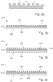
- Fig. 3a is a schematic illustration of a fingerprint sensing device 300 where the cover layer 302 comprises two separate sublayers.
- a first sublayer 304 is arranged to cover the sensing elements 204.
- the first sublayer 304 may for example be a mold layer used to protect the sensing elements 204 and to form an even surface on which the three-dimensional pattern can be formed.
- the second sublayer comprises a plurality of nanostructures 306 forming the three-dimensional pattern.
- Fig. 3b is a schematic illustration of a fingerprint sensing device 310 where the cover layer 312 comprises two separate sublayers, similar to as shown in Fig. 3a . However, in Fig. 3b , the nanostructures 314 are only formed in a portion of the second sublayer 316.
- Fig. 3c is a schematic illustration of a fingerprint sensing device 320 where the cover layer 322 can be said to comprise three sublayers, 304, 306 and 324, where the top surface of the nanostructures 306 are coated by a reflective material 324 to enhance the reflecting properties of the pattern in order to as efficiently as possible reflect the wavelengths which are not absorbed by the three-dimensional pattern.
- the reflective material 324 can for example be a metal.
- Fig. 3d is a schematic illustration of a fingerprint sensing device 330 where the cover layer 332 comprises a first sublayer 304 protecting the sensing elements, a second sublayer 334 comprising a reflective material, and a third sublayer comprising nanostructures 306 forming a three-dimensional pattern.
- the cover layer 332 comprises a first sublayer 304 protecting the sensing elements, a second sublayer 334 comprising a reflective material, and a third sublayer comprising nanostructures 306 forming a three-dimensional pattern.
- the reflective material cannot be electrically conductive as discussed above.
- the pattern may advantageously be configured to also provide hydrophobic or super-hydrophobic surface properties.
- Fig. 3e schematically illustrates a fingerprint sensing device 340 where the cover layer 342 comprises an additional sublayer 344 arranged to cover nanostructures 208 forming the three dimensional pattern.
- the additional layer 344 may for example be a mold layer arranged to protect the nanostructures 208.
- Fig. 3f schematically illustrates a fingerprint sensing device 350 where the cover layer 352 comprises a sublayer in the form of a protective plate 354 arranged to cover the three-dimensional pattern and to form an exterior surface 358, i.e. a sensing surface, of the fingerprint sensing device 350.
- the protective plate typically comprises a dielectric material in order to provide a good capacitive coupling between a finger placed on the plate and the sensing elements of the sensing chip.
- the protective plate may advantageously comprise a glass or ceramic material, such as a chemically strengthened glass, ZrO2 or sapphire.
- the aforementioned materials all provide advantageous properties in that they are hard and thereby resistant to wear and tear, and in that they are dielectric thereby providing a good capacitive coupling between a finger placed on the surface of the protective plate and the sensing element of the sensing device.
- the protective plate 354 can be attached to the sensing device using an adhesive 356 arranged between the pattern and the plate 354. The adhesive 356 can thus fill the spaces between the nanostructures so that no air is trapped in the device.
- the material covering the three-dimensional pattern is at least partially transparent to visible light so that light can reach the pattern.
- Fig. 4a is a schematic illustration of a fingerprint sensing device 400 according to an embodiment of the invention where different area portions 402a-c of the device 400 have different configurations of the three-dimensional pattern.
- Each area portion may be referred to as a sub-array or a color pixel 402a-c, which is not to be confused with the sensing element.
- Each color pixel can have a three-dimensional pattern configured to reduce the amount of reflected light within a specific predetermined sub-range of visible light.
- the pattern and/or the nanostructures may be varied in any of the ways discussed above so that each color pixel displays the desired color.
- the color pixels of the three dimensional pattern can have a size which is considerably smaller than the sensing element, thereby providing the possibility to form high resolution images on the surface of the sensing device 400.
- the color pixel may have a size in the range of 500 nm x 500 nm.
- Fig. 4b schematically illustrates a sensing device where different area portions of the device 408 comprises different types of diffraction gratings as illustrated by the saw-tooth patterns 410a-b and by the elongated ridges 412a-b, where the dimensions of the respective patterns are different to illustrate that each area portion can be tailored to reflect a desired wavelength spectrum. Accordingly, for a diffraction grating different shapes of the nanostructures can be used further to a plasmonic array.
- the illustrated color pixels also provides the possibility to combine plasmonic arrays with diffractive gratings in the same plane, where the technique used to achieve the desired color for each particular color pixel can be selected based on which technique provides the better result for the specific color.
- Fig. 5 is a flow chart outlining the general steps of a method according to an embodiment of the invention
- Figs. 6a-c are schematic illustrations outlining manufacturing steps according to an embodiment of the invention. The method will be described with reference to Figs. 6a-c illustrating a nanoimprint lithography method for forming a three-dimensional pattern in a fingerprint sensing device.
- a sensing chip 602 comprising sensing elements (not shown) is provided and the sensing chip is subsequently coated 504 with a cover layer 604 in which the pattern is to be formed.
- the cover layer can for example be a thermoplastic polymer resist.
- An imprint mold 606 is provided comprising a reversed/mirrored version of the pattern to be formed in the cover layer 604.
- the imprint mold 606 is being pressed onto the cover layer 604 while the cover layer 604 is being heated above the glass transition temperature so that the cover layer 604 becomes soft and deformable. Thereby, the pattern 608 is formed 506 in the cover layer 604.
- the sensing chip 602 and the imprint mold 606 is cooled so that the cover layer solidifies, leaving the sensing device with a three-dimensional pattern covering the sensing elements.
- the cover layer may also comprise a UV-curable material in which case the layer is illuminated by UV light to harden after the imprint mold has been pressed into the cover layer.
- Any additional layers described above with reference to Figs. 3a-f ⁇ can be formed using conventional and known manufacturing methods.
Landscapes
- Engineering & Computer Science (AREA)
- Human Computer Interaction (AREA)
- Physics & Mathematics (AREA)
- General Physics & Mathematics (AREA)
- Multimedia (AREA)
- Theoretical Computer Science (AREA)
- Measurement Of The Respiration, Hearing Ability, Form, And Blood Characteristics Of Living Organisms (AREA)
- Image Input (AREA)
- Measurement Of Length, Angles, Or The Like Using Electric Or Magnetic Means (AREA)
- Optical Modulation, Optical Deflection, Nonlinear Optics, Optical Demodulation, Optical Logic Elements (AREA)
Claims (13)
- Dispositif de détection d'empreintes digitales (200) comprenant :une puce de détection (202) comprenant un réseau d'éléments de détection (204), lesdits éléments de détection étant configurés pour être reliés à une circuiterie de lecture pour détecter un couplage capacitif entre chacun desdits éléments de détection et un doigt placé sur une surface de détection dudit dispositif de détection ;une couche de recouvrement (206) agencée verticalement au-dessus desdits éléments de détection pour recouvrir au moins une partie desdits éléments de détection, dans lequel une surface extérieure de ladite couche de recouvrement forme ladite surface de détection dudit dispositif de détection ;caractérisé en ce que ladite couche de recouvrement comprend un motif tridimensionnel (208, 410a-b, 412a-b) configuré pour réduire la quantité de lumière réfléchie à l'intérieur d'une sous-plage prédéterminée de la plage visible, le motif tridimensionnel étant un réseau plasmonique comprenant une pluralité de nanostructures électriquement conductrices (208), dans lequel lesdites nanostructures sont galvaniquement isolées les unes des autres.
- Dispositif de détection selon la revendication 1, dans lequel une taille, une forme et une répartition desdites nanostructures sont sélectionnées pour former un réseau plasmonique configuré pour réduire la quantité de lumière réfléchie à l'intérieur d'une sous-plage prédéterminée de la plage visible.
- Dispositif de détection selon l'une quelconque des revendications précédentes, dans lequel ladite couche de recouvrement comprend une pluralité de sous-couches.
- Dispositif de détection selon la revendication 1, dans lequel ledit motif tridimensionnel est agencé dans une première sous-couche qui est recouverte par une deuxième sous-couche.
- Dispositif de détection selon l'une quelconque des revendications précédentes, dans lequel ladite couche de recouvrement comprend une première partie d'aire dans laquelle ledit motif tridimensionnel est configuré pour réduire la quantité de lumière réfléchie à l'intérieur d'une première sous-plage prédéterminée, et une deuxième partie d'aire dans laquelle ledit motif tridimensionnel est configuré pour réduire la quantité de lumière réfléchie à l'intérieur d'une deuxième sous-plage prédéterminée, dans lequel ladite première sous-plage est différente de ladite deuxième sous-plage.
- Dispositif de détection selon l'une quelconque des revendications précédentes, dans lequel ledit motif tridimensionnel est agencé au niveau de ladite surface de détection, et dans lequel ledit motif est configuré pour fournir des propriétés de surface hydrophobes.
- Dispositif de détection selon l'une quelconque des revendications précédentes, dans lequel ledit motif tridimensionnel est configuré pour réduire la quantité de lumière réfléchie à l'intérieur de différentes sous-plages prédéterminées de la plage visible pour différentes parties d'aire du dispositif de détection de sorte qu'une image soit formée sur ladite surface de détection.
- Dispositif de détection selon l'une quelconque des revendications précédentes, dans lequel ledit motif tridimensionnel est configuré de sorte que la sous-plage prédéterminée soit différente pour différents angles de vision.
- Dispositif de détection selon l'une quelconque des revendications précédentes, dans lequel au moins une partie de ladite couche de recouvrement est revêtue d'un matériau optiquement réfléchissant.
- Dispositif de détection selon l'une quelconque des revendications précédentes, dans lequel au moins des parties saillantes dudit motif tridimensionnel sont revêtues d'un matériau optiquement réfléchissant.
- Procédé de fabrication d'un dispositif de détection d'empreintes digitales (200), ledit procédé comprenant :la fourniture (502) d'une puce de détection (202) comprenant un réseau d'éléments de détection (204), lesdits éléments de détection étant configurés pour être reliés à une circuiterie de lecture pour détecter un couplage capacitif entre chacun desdits éléments de détection et un doigt placé sur une surface de détection dudit dispositif de détection ;la formation (504) d'une couche de recouvrement (206) agencée verticalement au-dessus desdits éléments de détection pour recouvrir au moins une partie desdits éléments de détection, dans lequel une surface extérieure de ladite couche de recouvrement forme ladite surface de détection dudit dispositif de détection ; etle procédé étant caractérisé par, dans ladite couche de recouvrement, la formation (505) d'un motif tridimensionnel (208, 410a-b, 412a-b) configuré pour réduire la quantité de lumière réfléchie à l'intérieur d'une sous-plage prédéterminée de la plage visible, le motif tridimensionnel étant un réseau plasmonique comprenant une pluralité de nanostructures électriquement conductrices (208), dans lequel lesdites nanostructures sont galvaniquement isolées les unes des autres.
- Procédé selon la revendication 11, dans lequel ladite étape de formation d'un motif tridimensionnel comprend une lithographie par nano-impression ou une photolithographie.
- Procédé selon la revendication 11 ou 12, comprenant en outre le dépôt d'un revêtement réfléchissant sur des parties saillantes dudit motif tridimensionnel.
Applications Claiming Priority (2)
| Application Number | Priority Date | Filing Date | Title |
|---|---|---|---|
| SE1550957 | 2015-07-03 | ||
| PCT/SE2016/050637 WO2017007400A1 (fr) | 2015-07-03 | 2016-06-27 | Dispositif de détection d'empreintes digitales comprenant un motif tridimensionnel |
Publications (3)
| Publication Number | Publication Date |
|---|---|
| EP3317701A1 EP3317701A1 (fr) | 2018-05-09 |
| EP3317701A4 EP3317701A4 (fr) | 2018-12-26 |
| EP3317701B1 true EP3317701B1 (fr) | 2023-07-19 |
Family
ID=57685363
Family Applications (1)
| Application Number | Title | Priority Date | Filing Date |
|---|---|---|---|
| EP16821733.9A Active EP3317701B1 (fr) | 2015-07-03 | 2016-06-27 | Dispositif de détection d'empreintes digitales comprenant un motif tridimensionnel |
Country Status (6)
| Country | Link |
|---|---|
| US (1) | US9524416B1 (fr) |
| EP (1) | EP3317701B1 (fr) |
| JP (1) | JP6759253B2 (fr) |
| KR (1) | KR20180025862A (fr) |
| CN (1) | CN106662682B (fr) |
| WO (1) | WO2017007400A1 (fr) |
Families Citing this family (15)
| Publication number | Priority date | Publication date | Assignee | Title |
|---|---|---|---|---|
| US8485442B2 (en) | 2009-07-02 | 2013-07-16 | Biometric Payment Solutions | Electronic transaction verification system with biometric authentication |
| RU2765181C2 (ru) | 2015-07-06 | 2022-01-26 | Тёрнинг Поинт Терапьютикс, Инк. | Полиморфная форма диарильного макроцикла |
| EP3379391B1 (fr) * | 2017-01-19 | 2020-12-02 | Shenzhen Goodix Technology Co., Ltd. | Capteur d'empreintes digitales et procede pour sa fabrication |
| CN107808853B (zh) * | 2017-11-14 | 2019-09-24 | 苏州科阳光电科技有限公司 | 一种指纹芯片封装结构及制作方法、终端设备 |
| KR102808360B1 (ko) * | 2019-01-04 | 2025-05-19 | 삼성디스플레이 주식회사 | 지문 센서 및 이를 포함하는 표시 장치 |
| TWI742555B (zh) * | 2019-07-22 | 2021-10-11 | 神亞科技股份有限公司 | 成像系統 |
| CN111145071B (zh) * | 2019-12-23 | 2021-10-22 | 武汉大学 | 将水印叠加在连续灰度图像中的三通道超表面复用方法 |
| TWM608543U (zh) * | 2020-03-02 | 2021-03-01 | 神盾股份有限公司 | 整合式真手指光譜感測裝置 |
| WO2021197677A1 (fr) | 2020-04-02 | 2021-10-07 | Nil Technology Aps | Revêtements de métasurface |
| CN111461040B (zh) * | 2020-04-07 | 2024-11-19 | 武汉华星光电技术有限公司 | 电子设备及其光学指纹识别模组 |
| GB2621408A (en) * | 2022-08-12 | 2024-02-14 | Touch Biometrix Ltd | Sensors and methods |
| US20260065710A1 (en) * | 2022-08-12 | 2026-03-05 | Touch Biometrix Limited | Sensors and Methods |
| GB2621409A (en) * | 2022-08-12 | 2024-02-14 | Touch Biometrix Ltd | Sensors and methods |
| WO2024092243A1 (fr) * | 2022-10-28 | 2024-05-02 | Arizona Board Of Regents On Behalf Of The University Of Arizona | Substrats de miroir en verre pour réflexion non spéculaire |
| US20240322056A1 (en) * | 2023-03-21 | 2024-09-26 | Visera Technologies Company Ltd. | Optical device |
Citations (5)
| Publication number | Priority date | Publication date | Assignee | Title |
|---|---|---|---|---|
| US3968476A (en) * | 1974-07-17 | 1976-07-06 | Sperry Rand Corporation | Spurious signal removal in optical processor fingerprint identification apparatus |
| CA2529147A1 (fr) * | 2003-06-21 | 2005-01-06 | Aprilis, Inc. | Acquisition d'images biometriques haute resolution |
| KR20080050460A (ko) * | 2005-09-01 | 2008-06-05 | 루미다임 인크. | 생체계측 센서 |
| US20120249797A1 (en) * | 2010-02-28 | 2012-10-04 | Osterhout Group, Inc. | Head-worn adaptive display |
| US8284019B2 (en) * | 2007-05-08 | 2012-10-09 | Davar Pishva | Spectroscopic method and system for multi-factor biometric authentication |
Family Cites Families (25)
| Publication number | Priority date | Publication date | Assignee | Title |
|---|---|---|---|---|
| US4353056A (en) * | 1980-06-05 | 1982-10-05 | Siemens Corporation | Capacitive fingerprint sensor |
| US6411726B1 (en) * | 1998-10-08 | 2002-06-25 | Durel Corporation | Fingerprint detector using an EL lamp |
| JP2005055327A (ja) * | 2003-08-05 | 2005-03-03 | Sony Corp | 指紋照合装置 |
| EP1766547B1 (fr) * | 2004-06-18 | 2008-11-19 | Fingerprint Cards AB | Element de capteur d'empreinte digitale |
| TW200737486A (en) * | 2006-03-24 | 2007-10-01 | Lightuning Tech Inc | Semiconductor integrated circuit chip with nano-structure-surface resin passivation and method of fabricating the same |
| JP4621270B2 (ja) * | 2007-07-13 | 2011-01-26 | キヤノン株式会社 | 光学フィルタ |
| JP5300495B2 (ja) * | 2009-01-06 | 2013-09-25 | 株式会社東芝 | 選択的な光透過特性を有する金属薄膜複合体およびその製造方法 |
| KR101649700B1 (ko) * | 2009-12-28 | 2016-08-19 | 엘지디스플레이 주식회사 | 대면적 패터닝을 위한 마스터 몰드 제조방법 및 이를 이용한 표면 플라즈몬 컬러필터의 제조방법 |
| CA2796348C (fr) * | 2010-04-15 | 2016-01-12 | Authentec, Inc. | Capteur de doigt comprenant une lentille capacitive et procedes associes |
| EP2564247A2 (fr) * | 2010-04-27 | 2013-03-06 | The Regents Of The University Of Michigan | Dispositif d'affichage ayant des filtres de couleur plasmoniques et ayant des capacités photovoltaïques |
| US8724038B2 (en) * | 2010-10-18 | 2014-05-13 | Qualcomm Mems Technologies, Inc. | Wraparound assembly for combination touch, handwriting and fingerprint sensor |
| JP5080660B2 (ja) * | 2011-01-05 | 2012-11-21 | エイエスディ株式会社 | 指紋読取りセンサ |
| WO2012169656A1 (fr) * | 2011-06-09 | 2012-12-13 | Sharp Kabushiki Kaisha | Dispositif d'affichage réflectif plasmonique tactile et procédé pour modifier les couleurs réfléchies |
| DE102012108170B4 (de) * | 2012-09-03 | 2015-01-22 | Bundesdruckerei Gmbh | Sicherheitselement und Verfahren zur Herstellung eines Sicherheitselements |
| KR101974581B1 (ko) * | 2012-09-24 | 2019-05-02 | 삼성전자주식회사 | 3차원 나노플라즈모닉 구조체 및 이의 제조방법 |
| SG2013073085A (en) * | 2012-09-28 | 2014-04-28 | Agency Science Tech & Res | Method of writing to an optical data storage medium, method of reading from an optical data storage medium, and optical data storage medium |
| US9547107B2 (en) * | 2013-03-15 | 2017-01-17 | The Regents Of The University Of Michigan | Dye and pigment-free structural colors and angle-insensitive spectrum filters |
| US9984270B2 (en) * | 2013-08-05 | 2018-05-29 | Apple Inc. | Fingerprint sensor in an electronic device |
| US9418273B2 (en) * | 2013-09-18 | 2016-08-16 | Blackberry Limited | Structure for multicolor biometric scanning user interface |
| US9311545B2 (en) * | 2013-09-18 | 2016-04-12 | Blackberry Limited | Multicolor biometric scanning user interface |
| US20150124306A1 (en) * | 2013-11-06 | 2015-05-07 | Lehigh University | Ultrathin nanostructured metals for highly transmissive plasmonic subtractive color filters |
| KR101700998B1 (ko) * | 2014-01-02 | 2017-01-31 | 삼성전기주식회사 | 지문 감지 센서 및 이를 포함하는 전자 기기 |
| CN103955679B (zh) * | 2014-05-19 | 2017-12-15 | 上海天马微电子有限公司 | 彩膜基板、阵列基板和显示装置 |
| US9489604B2 (en) * | 2014-06-03 | 2016-11-08 | IE-9 Technology Corp. | Optically variable data storage device |
| US20160086044A1 (en) * | 2014-09-24 | 2016-03-24 | Au Optronics Corporation | Optical Device and Optical Scanning Method Thereof |
-
2016
- 2016-02-17 US US15/045,379 patent/US9524416B1/en active Active
- 2016-06-27 EP EP16821733.9A patent/EP3317701B1/fr active Active
- 2016-06-27 JP JP2017565962A patent/JP6759253B2/ja active Active
- 2016-06-27 CN CN201680002230.9A patent/CN106662682B/zh active Active
- 2016-06-27 WO PCT/SE2016/050637 patent/WO2017007400A1/fr not_active Ceased
- 2016-06-27 KR KR1020177036257A patent/KR20180025862A/ko not_active Ceased
Patent Citations (5)
| Publication number | Priority date | Publication date | Assignee | Title |
|---|---|---|---|---|
| US3968476A (en) * | 1974-07-17 | 1976-07-06 | Sperry Rand Corporation | Spurious signal removal in optical processor fingerprint identification apparatus |
| CA2529147A1 (fr) * | 2003-06-21 | 2005-01-06 | Aprilis, Inc. | Acquisition d'images biometriques haute resolution |
| KR20080050460A (ko) * | 2005-09-01 | 2008-06-05 | 루미다임 인크. | 생체계측 센서 |
| US8284019B2 (en) * | 2007-05-08 | 2012-10-09 | Davar Pishva | Spectroscopic method and system for multi-factor biometric authentication |
| US20120249797A1 (en) * | 2010-02-28 | 2012-10-04 | Osterhout Group, Inc. | Head-worn adaptive display |
Also Published As
| Publication number | Publication date |
|---|---|
| CN106662682B (zh) | 2018-01-09 |
| KR20180025862A (ko) | 2018-03-09 |
| WO2017007400A1 (fr) | 2017-01-12 |
| CN106662682A (zh) | 2017-05-10 |
| JP2018533030A (ja) | 2018-11-08 |
| EP3317701A4 (fr) | 2018-12-26 |
| JP6759253B2 (ja) | 2020-09-23 |
| US9524416B1 (en) | 2016-12-20 |
| US20170004342A1 (en) | 2017-01-05 |
| EP3317701A1 (fr) | 2018-05-09 |
Similar Documents
| Publication | Publication Date | Title |
|---|---|---|
| EP3317701B1 (fr) | Dispositif de détection d'empreintes digitales comprenant un motif tridimensionnel | |
| AU2022263490B2 (en) | An improved polymeric sheet material for use in making polymeric security documents such as banknotes | |
| US12253691B2 (en) | Optical products, masters for fabricating optical products, and methods for manufacturing masters and optical products | |
| TWI765870B (zh) | 薄膜及其製造方法、包含該薄膜的電性作用件及其製造方法 | |
| US10409331B2 (en) | Cover glass for electronic device | |
| JP5186378B2 (ja) | 多層体およびその製造方法 | |
| US7864424B2 (en) | Zero order pigments (ZOP) | |
| KR102414589B1 (ko) | 다층체 및 이를 제조하는 방법 | |
| CN106808835B (zh) | 光学防伪元件及其制备方法和光学防伪产品 | |
| CN105378514B (zh) | 日光管控 | |
| CA3195166A1 (fr) | Produits optiques, maitres de fabrication de produits optiques, et procedes de fabrication de maitres et de produits optiques | |
| TWI815976B (zh) | 光學可變化元件、防偽文件、光學可變化元件的製造方法、防偽文件的製造方法 | |
| US8133638B2 (en) | All-polymer grating microstructure | |
| JP7691538B2 (ja) | 完全マイクロ光学セキュリティドキュメント | |
| JP2014046667A (ja) | 情報表示媒体及びその真贋判定方法 | |
| KR20150064996A (ko) | 이중 색변환 보안장치 및 이를 포함하는 보안제품 | |
| JP6186837B2 (ja) | 表示体、表示体付き物品およびそれらの真偽判定方法 | |
| US12585132B2 (en) | Optical film for controlling optical path, and manufacturing method therefor | |
| WO2023082729A1 (fr) | Élément anti-contrefaçon et produit anti-contrefaçon | |
| JP6277712B2 (ja) | 表示体 | |
| CN114475043A (zh) | 光学防伪元件及其制作方法、防伪产品 | |
| WO2017164403A1 (fr) | Stratifié sensible aux ondes électromagnétiques | |
| WO2017199969A1 (fr) | Stratifié à résonance plasmonique, composition de formation de partie de liant, procédé permettant de fabriquer un stratifié à résonance plasmonique et support d'enregistrement d'informations |
Legal Events
| Date | Code | Title | Description |
|---|---|---|---|
| STAA | Information on the status of an ep patent application or granted ep patent |
Free format text: STATUS: THE INTERNATIONAL PUBLICATION HAS BEEN MADE |
|
| PUAI | Public reference made under article 153(3) epc to a published international application that has entered the european phase |
Free format text: ORIGINAL CODE: 0009012 |
|
| STAA | Information on the status of an ep patent application or granted ep patent |
Free format text: STATUS: REQUEST FOR EXAMINATION WAS MADE |
|
| 17P | Request for examination filed |
Effective date: 20171204 |
|
| AK | Designated contracting states |
Kind code of ref document: A1 Designated state(s): AL AT BE BG CH CY CZ DE DK EE ES FI FR GB GR HR HU IE IS IT LI LT LU LV MC MK MT NL NO PL PT RO RS SE SI SK SM TR |
|
| AX | Request for extension of the european patent |
Extension state: BA ME |
|
| DAV | Request for validation of the european patent (deleted) | ||
| DAX | Request for extension of the european patent (deleted) | ||
| A4 | Supplementary search report drawn up and despatched |
Effective date: 20181126 |
|
| RIC1 | Information provided on ipc code assigned before grant |
Ipc: B82Y 20/00 20110101ALI20181120BHEP Ipc: G06K 9/00 20060101ALI20181120BHEP Ipc: G01N 21/552 20140101ALI20181120BHEP Ipc: A61B 5/117 20160101ALI20181120BHEP Ipc: G02B 5/00 20060101AFI20181120BHEP Ipc: G02B 5/18 20060101ALI20181120BHEP |
|
| STAA | Information on the status of an ep patent application or granted ep patent |
Free format text: STATUS: EXAMINATION IS IN PROGRESS |
|
| 17Q | First examination report despatched |
Effective date: 20200423 |
|
| RAP1 | Party data changed (applicant data changed or rights of an application transferred) |
Owner name: FINGERPRINT CARDS ANACATUM IP AB |
|
| REG | Reference to a national code |
Ref country code: DE Ref legal event code: R079 Free format text: PREVIOUS MAIN CLASS: G02B0005000000 Ipc: G06V0040130000 Ref country code: DE Ref legal event code: R079 Ref document number: 602016081201 Country of ref document: DE Free format text: PREVIOUS MAIN CLASS: G02B0005000000 Ipc: G06V0040130000 |
|
| GRAP | Despatch of communication of intention to grant a patent |
Free format text: ORIGINAL CODE: EPIDOSNIGR1 |
|
| STAA | Information on the status of an ep patent application or granted ep patent |
Free format text: STATUS: GRANT OF PATENT IS INTENDED |
|
| RIC1 | Information provided on ipc code assigned before grant |
Ipc: G06V 40/13 20220101AFI20230206BHEP |
|
| INTG | Intention to grant announced |
Effective date: 20230220 |
|
| GRAS | Grant fee paid |
Free format text: ORIGINAL CODE: EPIDOSNIGR3 |
|
| GRAA | (expected) grant |
Free format text: ORIGINAL CODE: 0009210 |
|
| STAA | Information on the status of an ep patent application or granted ep patent |
Free format text: STATUS: THE PATENT HAS BEEN GRANTED |
|
| AK | Designated contracting states |
Kind code of ref document: B1 Designated state(s): AL AT BE BG CH CY CZ DE DK EE ES FI FR GB GR HR HU IE IS IT LI LT LU LV MC MK MT NL NO PL PT RO RS SE SI SK SM TR |
|
| REG | Reference to a national code |
Ref country code: GB Ref legal event code: FG4D |
|
| REG | Reference to a national code |
Ref country code: CH Ref legal event code: EP |
|
| REG | Reference to a national code |
Ref country code: DE Ref legal event code: R096 Ref document number: 602016081201 Country of ref document: DE |
|
| REG | Reference to a national code |
Ref country code: IE Ref legal event code: FG4D |
|
| REG | Reference to a national code |
Ref country code: LT Ref legal event code: MG9D |
|
| REG | Reference to a national code |
Ref country code: NL Ref legal event code: MP Effective date: 20230719 |
|
| REG | Reference to a national code |
Ref country code: AT Ref legal event code: MK05 Ref document number: 1590264 Country of ref document: AT Kind code of ref document: T Effective date: 20230719 |
|
| PG25 | Lapsed in a contracting state [announced via postgrant information from national office to epo] |
Ref country code: NL Free format text: LAPSE BECAUSE OF FAILURE TO SUBMIT A TRANSLATION OF THE DESCRIPTION OR TO PAY THE FEE WITHIN THE PRESCRIBED TIME-LIMIT Effective date: 20230719 |
|
| PG25 | Lapsed in a contracting state [announced via postgrant information from national office to epo] |
Ref country code: GR Free format text: LAPSE BECAUSE OF FAILURE TO SUBMIT A TRANSLATION OF THE DESCRIPTION OR TO PAY THE FEE WITHIN THE PRESCRIBED TIME-LIMIT Effective date: 20231020 |
|
| PG25 | Lapsed in a contracting state [announced via postgrant information from national office to epo] |
Ref country code: IS Free format text: LAPSE BECAUSE OF FAILURE TO SUBMIT A TRANSLATION OF THE DESCRIPTION OR TO PAY THE FEE WITHIN THE PRESCRIBED TIME-LIMIT Effective date: 20231119 |
|
| PG25 | Lapsed in a contracting state [announced via postgrant information from national office to epo] |
Ref country code: SE Free format text: LAPSE BECAUSE OF FAILURE TO SUBMIT A TRANSLATION OF THE DESCRIPTION OR TO PAY THE FEE WITHIN THE PRESCRIBED TIME-LIMIT Effective date: 20230719 Ref country code: RS Free format text: LAPSE BECAUSE OF FAILURE TO SUBMIT A TRANSLATION OF THE DESCRIPTION OR TO PAY THE FEE WITHIN THE PRESCRIBED TIME-LIMIT Effective date: 20230719 Ref country code: PT Free format text: LAPSE BECAUSE OF FAILURE TO SUBMIT A TRANSLATION OF THE DESCRIPTION OR TO PAY THE FEE WITHIN THE PRESCRIBED TIME-LIMIT Effective date: 20231120 Ref country code: NO Free format text: LAPSE BECAUSE OF FAILURE TO SUBMIT A TRANSLATION OF THE DESCRIPTION OR TO PAY THE FEE WITHIN THE PRESCRIBED TIME-LIMIT Effective date: 20231019 Ref country code: LV Free format text: LAPSE BECAUSE OF FAILURE TO SUBMIT A TRANSLATION OF THE DESCRIPTION OR TO PAY THE FEE WITHIN THE PRESCRIBED TIME-LIMIT Effective date: 20230719 Ref country code: LT Free format text: LAPSE BECAUSE OF FAILURE TO SUBMIT A TRANSLATION OF THE DESCRIPTION OR TO PAY THE FEE WITHIN THE PRESCRIBED TIME-LIMIT Effective date: 20230719 Ref country code: IS Free format text: LAPSE BECAUSE OF FAILURE TO SUBMIT A TRANSLATION OF THE DESCRIPTION OR TO PAY THE FEE WITHIN THE PRESCRIBED TIME-LIMIT Effective date: 20231119 Ref country code: HR Free format text: LAPSE BECAUSE OF FAILURE TO SUBMIT A TRANSLATION OF THE DESCRIPTION OR TO PAY THE FEE WITHIN THE PRESCRIBED TIME-LIMIT Effective date: 20230719 Ref country code: GR Free format text: LAPSE BECAUSE OF FAILURE TO SUBMIT A TRANSLATION OF THE DESCRIPTION OR TO PAY THE FEE WITHIN THE PRESCRIBED TIME-LIMIT Effective date: 20231020 Ref country code: FI Free format text: LAPSE BECAUSE OF FAILURE TO SUBMIT A TRANSLATION OF THE DESCRIPTION OR TO PAY THE FEE WITHIN THE PRESCRIBED TIME-LIMIT Effective date: 20230719 Ref country code: AT Free format text: LAPSE BECAUSE OF FAILURE TO SUBMIT A TRANSLATION OF THE DESCRIPTION OR TO PAY THE FEE WITHIN THE PRESCRIBED TIME-LIMIT Effective date: 20230719 |
|
| PG25 | Lapsed in a contracting state [announced via postgrant information from national office to epo] |
Ref country code: PL Free format text: LAPSE BECAUSE OF FAILURE TO SUBMIT A TRANSLATION OF THE DESCRIPTION OR TO PAY THE FEE WITHIN THE PRESCRIBED TIME-LIMIT Effective date: 20230719 |
|
| REG | Reference to a national code |
Ref country code: DE Ref legal event code: R097 Ref document number: 602016081201 Country of ref document: DE |
|
| PG25 | Lapsed in a contracting state [announced via postgrant information from national office to epo] |
Ref country code: ES Free format text: LAPSE BECAUSE OF FAILURE TO SUBMIT A TRANSLATION OF THE DESCRIPTION OR TO PAY THE FEE WITHIN THE PRESCRIBED TIME-LIMIT Effective date: 20230719 |
|
| PG25 | Lapsed in a contracting state [announced via postgrant information from national office to epo] |
Ref country code: SM Free format text: LAPSE BECAUSE OF FAILURE TO SUBMIT A TRANSLATION OF THE DESCRIPTION OR TO PAY THE FEE WITHIN THE PRESCRIBED TIME-LIMIT Effective date: 20230719 Ref country code: RO Free format text: LAPSE BECAUSE OF FAILURE TO SUBMIT A TRANSLATION OF THE DESCRIPTION OR TO PAY THE FEE WITHIN THE PRESCRIBED TIME-LIMIT Effective date: 20230719 Ref country code: ES Free format text: LAPSE BECAUSE OF FAILURE TO SUBMIT A TRANSLATION OF THE DESCRIPTION OR TO PAY THE FEE WITHIN THE PRESCRIBED TIME-LIMIT Effective date: 20230719 Ref country code: EE Free format text: LAPSE BECAUSE OF FAILURE TO SUBMIT A TRANSLATION OF THE DESCRIPTION OR TO PAY THE FEE WITHIN THE PRESCRIBED TIME-LIMIT Effective date: 20230719 Ref country code: DK Free format text: LAPSE BECAUSE OF FAILURE TO SUBMIT A TRANSLATION OF THE DESCRIPTION OR TO PAY THE FEE WITHIN THE PRESCRIBED TIME-LIMIT Effective date: 20230719 Ref country code: CZ Free format text: LAPSE BECAUSE OF FAILURE TO SUBMIT A TRANSLATION OF THE DESCRIPTION OR TO PAY THE FEE WITHIN THE PRESCRIBED TIME-LIMIT Effective date: 20230719 Ref country code: SK Free format text: LAPSE BECAUSE OF FAILURE TO SUBMIT A TRANSLATION OF THE DESCRIPTION OR TO PAY THE FEE WITHIN THE PRESCRIBED TIME-LIMIT Effective date: 20230719 |
|
| PLBE | No opposition filed within time limit |
Free format text: ORIGINAL CODE: 0009261 |
|
| STAA | Information on the status of an ep patent application or granted ep patent |
Free format text: STATUS: NO OPPOSITION FILED WITHIN TIME LIMIT |
|
| PG25 | Lapsed in a contracting state [announced via postgrant information from national office to epo] |
Ref country code: IT Free format text: LAPSE BECAUSE OF FAILURE TO SUBMIT A TRANSLATION OF THE DESCRIPTION OR TO PAY THE FEE WITHIN THE PRESCRIBED TIME-LIMIT Effective date: 20230719 |
|
| 26N | No opposition filed |
Effective date: 20240422 |
|
| PGFP | Annual fee paid to national office [announced via postgrant information from national office to epo] |
Ref country code: GB Payment date: 20240627 Year of fee payment: 9 |
|
| PGFP | Annual fee paid to national office [announced via postgrant information from national office to epo] |
Ref country code: DE Payment date: 20240627 Year of fee payment: 9 |
|
| PG25 | Lapsed in a contracting state [announced via postgrant information from national office to epo] |
Ref country code: SI Free format text: LAPSE BECAUSE OF FAILURE TO SUBMIT A TRANSLATION OF THE DESCRIPTION OR TO PAY THE FEE WITHIN THE PRESCRIBED TIME-LIMIT Effective date: 20230719 |
|
| PGFP | Annual fee paid to national office [announced via postgrant information from national office to epo] |
Ref country code: FR Payment date: 20240625 Year of fee payment: 9 |
|
| PG25 | Lapsed in a contracting state [announced via postgrant information from national office to epo] |
Ref country code: BG Free format text: LAPSE BECAUSE OF FAILURE TO SUBMIT A TRANSLATION OF THE DESCRIPTION OR TO PAY THE FEE WITHIN THE PRESCRIBED TIME-LIMIT Effective date: 20230719 |
|
| PG25 | Lapsed in a contracting state [announced via postgrant information from national office to epo] |
Ref country code: BG Free format text: LAPSE BECAUSE OF FAILURE TO SUBMIT A TRANSLATION OF THE DESCRIPTION OR TO PAY THE FEE WITHIN THE PRESCRIBED TIME-LIMIT Effective date: 20230719 |
|
| PG25 | Lapsed in a contracting state [announced via postgrant information from national office to epo] |
Ref country code: MC Free format text: LAPSE BECAUSE OF FAILURE TO SUBMIT A TRANSLATION OF THE DESCRIPTION OR TO PAY THE FEE WITHIN THE PRESCRIBED TIME-LIMIT Effective date: 20230719 |
|
| REG | Reference to a national code |
Ref country code: CH Ref legal event code: PL |
|
| PG25 | Lapsed in a contracting state [announced via postgrant information from national office to epo] |
Ref country code: LU Free format text: LAPSE BECAUSE OF NON-PAYMENT OF DUE FEES Effective date: 20240627 |
|
| PG25 | Lapsed in a contracting state [announced via postgrant information from national office to epo] |
Ref country code: IE Free format text: LAPSE BECAUSE OF NON-PAYMENT OF DUE FEES Effective date: 20240627 |
|
| PG25 | Lapsed in a contracting state [announced via postgrant information from national office to epo] |
Ref country code: CH Free format text: LAPSE BECAUSE OF NON-PAYMENT OF DUE FEES Effective date: 20240630 Ref country code: BE Free format text: LAPSE BECAUSE OF NON-PAYMENT OF DUE FEES Effective date: 20240630 |
|
| REG | Reference to a national code |
Ref country code: BE Ref legal event code: MM Effective date: 20240630 |
|
| PG25 | Lapsed in a contracting state [announced via postgrant information from national office to epo] |
Ref country code: CY Free format text: LAPSE BECAUSE OF FAILURE TO SUBMIT A TRANSLATION OF THE DESCRIPTION OR TO PAY THE FEE WITHIN THE PRESCRIBED TIME-LIMIT; INVALID AB INITIO Effective date: 20160627 |
|
| REG | Reference to a national code |
Ref country code: DE Ref legal event code: R119 Ref document number: 602016081201 Country of ref document: DE |
|
| GBPC | Gb: european patent ceased through non-payment of renewal fee |
Effective date: 20250627 |
|
| PG25 | Lapsed in a contracting state [announced via postgrant information from national office to epo] |
Ref country code: HU Free format text: LAPSE BECAUSE OF FAILURE TO SUBMIT A TRANSLATION OF THE DESCRIPTION OR TO PAY THE FEE WITHIN THE PRESCRIBED TIME-LIMIT; INVALID AB INITIO Effective date: 20160627 |
|
| PG25 | Lapsed in a contracting state [announced via postgrant information from national office to epo] |
Ref country code: GB Free format text: LAPSE BECAUSE OF NON-PAYMENT OF DUE FEES Effective date: 20250627 |
|
| PG25 | Lapsed in a contracting state [announced via postgrant information from national office to epo] |
Ref country code: DE Free format text: LAPSE BECAUSE OF NON-PAYMENT OF DUE FEES Effective date: 20260101 |
|
| PG25 | Lapsed in a contracting state [announced via postgrant information from national office to epo] |
Ref country code: FR Free format text: LAPSE BECAUSE OF NON-PAYMENT OF DUE FEES Effective date: 20250630 |