EP3320403B1 - Verfahren zur fixierung durch anodische verbindung - Google Patents
Verfahren zur fixierung durch anodische verbindung Download PDFInfo
- Publication number
- EP3320403B1 EP3320403B1 EP16734046.2A EP16734046A EP3320403B1 EP 3320403 B1 EP3320403 B1 EP 3320403B1 EP 16734046 A EP16734046 A EP 16734046A EP 3320403 B1 EP3320403 B1 EP 3320403B1
- Authority
- EP
- European Patent Office
- Prior art keywords
- anodic bonding
- bonding method
- assembly
- previous
- intermediate layer
- Prior art date
- Legal status (The legal status is an assumption and is not a legal conclusion. Google has not performed a legal analysis and makes no representation as to the accuracy of the status listed.)
- Active
Links
Images


Classifications
-
- G—PHYSICS
- G04—HOROLOGY
- G04B—MECHANICALLY-DRIVEN CLOCKS OR WATCHES; MECHANICAL PARTS OF CLOCKS OR WATCHES IN GENERAL; TIME PIECES USING THE POSITION OF THE SUN, MOON OR STARS
- G04B39/00—Watch crystals; Fastening or sealing of crystals; Clock glasses
- G04B39/02—Sealing crystals or glasses
- G04B39/025—Sealing crystals or glasses without special sealing parts
-
- C—CHEMISTRY; METALLURGY
- C03—GLASS; MINERAL OR SLAG WOOL
- C03C—CHEMICAL COMPOSITION OF GLASSES, GLAZES OR VITREOUS ENAMELS; SURFACE TREATMENT OF GLASS; SURFACE TREATMENT OF FIBRES OR FILAMENTS MADE FROM GLASS, MINERALS OR SLAGS; JOINING GLASS TO GLASS OR OTHER MATERIALS
- C03C27/00—Joining pieces of glass to pieces of other inorganic material; Joining glass to glass other than by fusing
-
- C—CHEMISTRY; METALLURGY
- C03—GLASS; MINERAL OR SLAG WOOL
- C03C—CHEMICAL COMPOSITION OF GLASSES, GLAZES OR VITREOUS ENAMELS; SURFACE TREATMENT OF GLASS; SURFACE TREATMENT OF FIBRES OR FILAMENTS MADE FROM GLASS, MINERALS OR SLAGS; JOINING GLASS TO GLASS OR OTHER MATERIALS
- C03C27/00—Joining pieces of glass to pieces of other inorganic material; Joining glass to glass other than by fusing
- C03C27/02—Joining pieces of glass to pieces of other inorganic material; Joining glass to glass other than by fusing by fusing glass directly to metal
-
- C—CHEMISTRY; METALLURGY
- C03—GLASS; MINERAL OR SLAG WOOL
- C03C—CHEMICAL COMPOSITION OF GLASSES, GLAZES OR VITREOUS ENAMELS; SURFACE TREATMENT OF GLASS; SURFACE TREATMENT OF FIBRES OR FILAMENTS MADE FROM GLASS, MINERALS OR SLAGS; JOINING GLASS TO GLASS OR OTHER MATERIALS
- C03C27/00—Joining pieces of glass to pieces of other inorganic material; Joining glass to glass other than by fusing
- C03C27/06—Joining glass to glass by processes other than fusing
-
- G—PHYSICS
- G04—HOROLOGY
- G04B—MECHANICALLY-DRIVEN CLOCKS OR WATCHES; MECHANICAL PARTS OF CLOCKS OR WATCHES IN GENERAL; TIME PIECES USING THE POSITION OF THE SUN, MOON OR STARS
- G04B19/00—Indicating the time by visual means
- G04B19/06—Dials
-
- G—PHYSICS
- G04—HOROLOGY
- G04B—MECHANICALLY-DRIVEN CLOCKS OR WATCHES; MECHANICAL PARTS OF CLOCKS OR WATCHES IN GENERAL; TIME PIECES USING THE POSITION OF THE SUN, MOON OR STARS
- G04B37/00—Cases
- G04B37/22—Materials or processes of manufacturing pocket watch or wrist watch cases
-
- H—ELECTRICITY
- H10—SEMICONDUCTOR DEVICES; ELECTRIC SOLID-STATE DEVICES NOT OTHERWISE PROVIDED FOR
- H10P—GENERIC PROCESSES OR APPARATUS FOR THE MANUFACTURE OR TREATMENT OF DEVICES COVERED BY CLASS H10
- H10P90/00—Preparation of wafers not covered by a single main group of this subclass, e.g. wafer reinforcement
- H10P90/19—Preparing inhomogeneous wafers
- H10P90/1904—Preparing vertically inhomogeneous wafers
- H10P90/1906—Preparing SOI wafers
- H10P90/1914—Preparing SOI wafers using bonding
-
- B—PERFORMING OPERATIONS; TRANSPORTING
- B23—MACHINE TOOLS; METAL-WORKING NOT OTHERWISE PROVIDED FOR
- B23K—SOLDERING OR UNSOLDERING; WELDING; CLADDING OR PLATING BY SOLDERING OR WELDING; CUTTING BY APPLYING HEAT LOCALLY, e.g. FLAME CUTTING; WORKING BY LASER BEAM
- B23K1/00—Soldering, e.g. brazing, or unsoldering
- B23K1/0004—Resistance soldering
-
- B—PERFORMING OPERATIONS; TRANSPORTING
- B29—WORKING OF PLASTICS; WORKING OF SUBSTANCES IN A PLASTIC STATE IN GENERAL
- B29C—SHAPING OR JOINING OF PLASTICS; SHAPING OF MATERIAL IN A PLASTIC STATE, NOT OTHERWISE PROVIDED FOR; AFTER-TREATMENT OF THE SHAPED PRODUCTS, e.g. REPAIRING
- B29C65/00—Joining or sealing of preformed parts, e.g. welding of plastics materials; Apparatus therefor
- B29C65/002—Joining methods not otherwise provided for
- B29C65/006—Diffusion joining
-
- B—PERFORMING OPERATIONS; TRANSPORTING
- B29—WORKING OF PLASTICS; WORKING OF SUBSTANCES IN A PLASTIC STATE IN GENERAL
- B29C—SHAPING OR JOINING OF PLASTICS; SHAPING OF MATERIAL IN A PLASTIC STATE, NOT OTHERWISE PROVIDED FOR; AFTER-TREATMENT OF THE SHAPED PRODUCTS, e.g. REPAIRING
- B29C65/00—Joining or sealing of preformed parts, e.g. welding of plastics materials; Apparatus therefor
- B29C65/02—Joining or sealing of preformed parts, e.g. welding of plastics materials; Apparatus therefor by heating, with or without pressure
- B29C65/04—Dielectric heating, e.g. high-frequency welding, i.e. radio frequency welding of plastic materials having dielectric properties, e.g. PVC
-
- C—CHEMISTRY; METALLURGY
- C03—GLASS; MINERAL OR SLAG WOOL
- C03C—CHEMICAL COMPOSITION OF GLASSES, GLAZES OR VITREOUS ENAMELS; SURFACE TREATMENT OF GLASS; SURFACE TREATMENT OF FIBRES OR FILAMENTS MADE FROM GLASS, MINERALS OR SLAGS; JOINING GLASS TO GLASS OR OTHER MATERIALS
- C03C27/00—Joining pieces of glass to pieces of other inorganic material; Joining glass to glass other than by fusing
- C03C27/06—Joining glass to glass by processes other than fusing
- C03C27/08—Joining glass to glass by processes other than fusing with the aid of intervening metal
-
- G—PHYSICS
- G04—HOROLOGY
- G04B—MECHANICALLY-DRIVEN CLOCKS OR WATCHES; MECHANICAL PARTS OF CLOCKS OR WATCHES IN GENERAL; TIME PIECES USING THE POSITION OF THE SUN, MOON OR STARS
- G04B37/00—Cases
- G04B37/08—Hermetic sealing of openings, joints, passages or slits
- G04B37/11—Hermetic sealing of openings, joints, passages or slits of the back cover of pocket or wrist watches
-
- G—PHYSICS
- G04—HOROLOGY
- G04B—MECHANICALLY-DRIVEN CLOCKS OR WATCHES; MECHANICAL PARTS OF CLOCKS OR WATCHES IN GENERAL; TIME PIECES USING THE POSITION OF THE SUN, MOON OR STARS
- G04B39/00—Watch crystals; Fastening or sealing of crystals; Clock glasses
- G04B39/002—Watch crystals; Fastening or sealing of crystals; Clock glasses made of glass
-
- G—PHYSICS
- G04—HOROLOGY
- G04B—MECHANICALLY-DRIVEN CLOCKS OR WATCHES; MECHANICAL PARTS OF CLOCKS OR WATCHES IN GENERAL; TIME PIECES USING THE POSITION OF THE SUN, MOON OR STARS
- G04B39/00—Watch crystals; Fastening or sealing of crystals; Clock glasses
- G04B39/004—Watch crystals; Fastening or sealing of crystals; Clock glasses from a material other than glass
- G04B39/006—Watch crystals; Fastening or sealing of crystals; Clock glasses from a material other than glass out of wear resistant material, e.g. sapphire
-
- G—PHYSICS
- G04—HOROLOGY
- G04B—MECHANICALLY-DRIVEN CLOCKS OR WATCHES; MECHANICAL PARTS OF CLOCKS OR WATCHES IN GENERAL; TIME PIECES USING THE POSITION OF THE SUN, MOON OR STARS
- G04B39/00—Watch crystals; Fastening or sealing of crystals; Clock glasses
- G04B39/02—Sealing crystals or glasses
-
- H—ELECTRICITY
- H10—SEMICONDUCTOR DEVICES; ELECTRIC SOLID-STATE DEVICES NOT OTHERWISE PROVIDED FOR
- H10P—GENERIC PROCESSES OR APPARATUS FOR THE MANUFACTURE OR TREATMENT OF DEVICES COVERED BY CLASS H10
- H10P95/00—Generic processes or apparatus for manufacture or treatments not covered by the other groups of this subclass
- H10P95/80—Electrical treatments, e.g. for electroforming
Definitions
- the present invention relates to a method of anodic assembly between two elements with an intermediate layer, in particular, but not exclusively, the present invention relates to a method of anodic assembly between a metallic element and a heterogeneous element, such as for example a glass , a synthetic crystal, such as for example a sapphire, or a ceramic.
- a metallic element and a heterogeneous element such as for example a glass , a synthetic crystal, such as for example a sapphire, or a ceramic.
- the specificity and the aim of the present invention is to produce a gas-tight and liquid-tight assembly without welding, without soldering and without organic compound (adhesive).
- the present method makes it possible to attach a watch crystal which can typically be made of mineral glass, sapphire or other transparent or translucent ceramics, to a bezel or middle-bezel of a watch case by the technique of anodic bonding.
- the area of the watch case on which the crystal is fixed is typically made of stainless steel, platinum, gold, titanium or one of the alloys associated with these materials.
- the aforementioned materials can either be coated with rhodium or any other material used for the manufacture of watch cases or of jewelery products.
- the glass can be totally or partially coated with an anti-reflective layer, without this interfering with the assembly process.
- the present invention also allows the fixing of the bottom windows. It is also possible, by the method of the invention, to attach drive elements to a transparent blade, thus producing an invisible gear, or a mysterious watch.
- the anodic bonding process is used in the general field of microtechnology, more particularly in biomedical, aerospace and electronics sectors.
- anode assemblies are mainly used for films and thin and flat layers in particular as wafers of metal, glass and silicon. Since the process requires relatively high temperatures, it is generally used to assemble materials with close coefficients of thermal expansion, in order to limit the constraints linked to differences in contraction.
- the anodic assembly is mainly reserved for joining glass, in particular Pyrex® or borofloat® glass (borosilicate glasses).
- the document BE680529 A4 discloses assembly methods by anodic connection between several substrates with a pulsed electric voltage or AC
- CH678680 A3 discloses a method of assembling a watch crystal by welding. This document recommends the use of a tin or lead solder alloy and the deposition of a layer or several layers of weldable material such as Ag, In, Bi, Au, Cu.
- An object of the present invention is to provide an assembly method free from the limitations of known anode assembly methods, in particular a method making it possible to obtain stronger bonds. and waterproof.
- the process takes place at low temperature, much lower than the transition or melting temperatures of the materials used.
- Another object of the present invention is to provide an anodic assembly process which allows the union of heterogeneous materials, without being limited to borosilicate glasses.
- the assembly described makes it possible to make metal to metal, metal to non-metal and non-metal to non-metal connections.
- the low temperatures involved in the process of the invention also allow it to be applied to assemblies comprising elements made of synthetic and / or composite materials.
- the assembly proposed by the present invention allows the binding of a large number of materials through intermediate layers, this in order to consolidate the link, increase the speed of diffusion and allow the assembly for a greater range of materials and more massive parts, subjected to strong constraints and having to resist shocks.
- the intermediate layer is an insulating or semiconductive layer. It can be an insert (for example a thin glass slide) or, preferably, a layer deposited by a physical or chemical deposition process (PVD, PE-CVD, Sol-gel, electroplating). Alternatively, the intermediate layer can be a natural or forced passivation layer, for example an oxide layer on a metallic element made of steel or titanium.
- the elements of the assembly are brought into intimate contact at the atomic level by an electric field of sufficient intensity. It is believed, without wishing to be limited by theory, that the application of an electric field allows the migration of atoms and ions in and of the intermediate layer, as well as the creation of chemical and charge gradients, thus giving rise to covalent and / or ionic links between the elements of the assembly.
- the electric field has a variable component, pulsed or alternating, and a continuous component.
- the characteristic frequencies of the pulsed or alternating variable component are essentially above the dielectric relaxation frequency of the materials used and are between 0.1 and 100 kHz.
- the stability and strength of the anode link can be considerably improved by functionalizing the surfaces before the application of the electric field by plasma bombardment, in particular by oxygen-rich plasmas.
- the present description has presented examples related to the manufacture of watches, the present invention also has other applications in watchmaking, and also in jewelry, leather goods, eyewear, and the production of writing instruments.
- the invention is also not limited to the production of decorative elements, but also allows the assembly of composite technical elements for watch movements, optical instruments, medical devices, and a wide variety of 'articles and products that use glass or ceramics.
- the method of the invention is applied to the fixing of a watch crystal on a case or on a watch bezel. It should however be understood that the invention can also be applied to the assembly of any other object or component. The description will be better understood with reference to FIG. 1a which represents, in section, an assembly as described in an anode assembly device.
- the part intended to receive the ice can be produced by any known method, for example by machining, stamping, rolling, 3D printing, or any other method. It is important that the face in contact with the ice is perfectly flat and free of roughness on a microscopic scale, to allow intimate contact. Depending on the needs and the nature of the materials used, this can be obtained by mechanical and / or electrochemical polishing, for example.
- the contact surface of the glass is chemically or mechanically polished in order to perfectly match the corresponding surface of the telescope and / or the notch.
- An intermediate layer 23 is then developed on the contact surface of the telescope 20, and / or of the crystal 10.
- this is a thin layer deposited by a physical or chemical deposition process (PVD, PE-CVD, Sol-gel, electroplating).
- PVD physical or chemical deposition process
- PE-CVD PE-CVD
- Sol-gel electroplating
- metallic layers deposited by a PVD process for example layers of oxidized titanium, or by natural oxidation layers functionalized by oxygen-rich plasma.
- the process of the invention does not require a homogeneous chemical composition of the intermediate layer 23.
- layers having a chemical and / or oxidation gradient have provided superior results in terms of adhesion, solidity of the connection and speed of assembly.
- the intermediate layer 23 has a thickness between 1 nm and 10 ⁇ m and its composition varies from pure titanium, in the deeper regions, to TiO 2 oxide on the surface, passing through all the intermediate stoichiometries. As will be seen later, it is advantageous to accentuate this chemical gradient with exposures to a reactive plasma.
- Titanium layers as we say, have given excellent results, but the invention can be replicated with other materials, for example Zr, Hf, Fe, Si , Al, Cr, Ni, invar among others.
- the chemical gradient can be obtained by oxidation, nitriding, carburation, for example, so that the composition of the layer can be of the Ti x O y , Si x O y , Si x N y , or Al x O y type .
- the intermediate layer can be enriched by mobile atoms / ions such as Li, Na, K, Ca, Be, or halogens.
- the intermediate layer 23 can be a layer of natural oxide, developing spontaneously following exposure to air, or forced, by exposure to a reactive atmosphere or plasma.
- the intermediate layer 23 can be obtained, in variants of the invention, by a process of physical deposition in a reactive atmosphere of variable composition.
- a process of physical deposition in a reactive atmosphere of variable composition One can for example deposit a layer by sputtering, in an inert atmosphere, in a first phase, and with a progressively increasing concentration of reactive gas (typically oxygen) thereafter.
- the layer 23 is activated by exposure to a plasma chemically at the same time as it is deposited. By this process, layers with the desired chemical gradient can be obtained.
- the intermediate layer can be an insert, for example a thin glass slide.
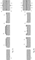
- Figure la very schematically shows an assembly device for carrying out the inventive process.
- the glass 10 is positioned on the upper face of the telescope 20 in an enclosure 40.
- Heating means 45 make it possible to maintain the parts at a desired temperature.
- the invention takes place at temperatures lower than those of conventional anode assembly processes.
- the temperature is preferably below 250 ° C. Very satisfactory results have been obtained at temperatures of 200 ° C, 150 ° C, 100 ° C, and even 75 ° C. In no case will the temperature be close to that of melting or glass transition of the materials used.
- the glass is connected to an electrode 31 and the telescope is connected to a counter electrode 32, to which a voltage source 30 is connected.
- the voltage source produces an electric field which generates an ion migration between the part 20, the layer 23 and Exhibit 10.
- the voltage generated by the source 30 comprises a direct component (its mean value or DC offset voltage) within the limits of what is generally used in anodic assembly processes, that is to say in the range 0.1-15 kV, depending on the thickness of the parts to be joined and the dielectric strength of the assembly.
- a direct component (its mean value or DC offset voltage) within the limits of what is generally used in anodic assembly processes, that is to say in the range 0.1-15 kV, depending on the thickness of the parts to be joined and the dielectric strength of the assembly.
- the amplitude of the AC component or the height of the pulses is preferably comparable to that of the DC component, and the characteristic frequency will be greater than 100 Hz, for example 1 kHz, 10 kHz, or more.
- the characteristic frequency of the AC component or of the pulses is also preferably greater than the dielectric relaxation frequencies of the materials used.
- the parts 20, 10 can be mechanically compressed. However, it has been found that if the contact surfaces are meticulously polished and clean, such plating is often superfluous.
- the assembly speeds are of the order of a few mm 2 / minutes.
- intermediate layer 23 and the substrate 20 can be deposited thin layers with an aesthetic or physical function such as anti-reflection functions (if the substrate 20 is transparent, for example), or to improve adhesion, or for any other purpose .
- additional layers are not shown in the figures.
- the transition between layer materials can be discontinuous or gradual.
- the method of the invention is not limited to the assembly of two elements.
- the figure 1b schematically illustrates an assembly with an intermediate substrate 15 between the first element 10 and the second element 20. Intermediate layers 13, 23 are present at each interface. The number of overlapping elements can be increased at will.
- transport phenomena The properties relating to electric currents and to the movements of charge carriers under the influence of applied forces are called transport phenomena.
- transport phenomena mobility, whether for example gaps, impurities, charge carriers (the materials are differentiated by the Debye length of the majority carriers and their behavior is notably described by the equation of continuity ) as well as diffusion (based on Fick's laws) are the key mechanisms of anodic assembly.
- the parameters which most influence the mobility of the charge carriers are the temperature and the volume number of impurities. Among the defects one can distinguish the impurities and the gaps. These are the same gaps, Schottky or Frenkel faults among others which facilitate the diffusion of charge carriers and which define the energy necessary for their diffusion. In addition moving a gap through a crystal requires much less work than forcing an ion to move through a dense ion network of a crystal. Ion conduction depends on the movement of the vacancies.
- the impurities which contribute to the density of charge carriers are called “donors” if they provide additional electrons and “acceptors” if they provide additional holes. Note that the speed of phenomenon of anodic assembly depends on the quantity of defects and on the temperature in particular.
- the choice of the intermediate layer or layers strongly depends on the "properties" of the charge carriers.
- the chemical composition of the layer or layers is naturally important since the transport phenomena depend on the characteristics of the atomic bonds.
- the bonds created during the anodic assembly process are mostly covalent type bonds. These strong bonds are established by the pooling of a pair of electrons from each of the charge carriers.
- the thickness limitations depend on the tolerances in terms of glasses and lenses and are between 1-1000 nm.
- the figure 2 schematically represents a succession of steps of the inventive process.
- the part 20, machined and polished is first cleaned (step a) by leaching baths, or by ultrasound, or by any suitable washing process 50.
- step b) an intermediate assembly layer is created by PVD deposition 55, as discussed above, or by any other suitable method.
- Step c) represents the element 20 with the intermediate layer 23 activated (the element 10 with another intermediate layer 13 is not shown in step c) of the figure).
- the surface or surfaces to be joined are preferably activated by a bombardment of reactive plasma 60 (step d).
- the chemical and physical characteristics of the plasma will be chosen according to the chemistry desired for the intermediate layer. For example, oxygen plasmas applied to titanium or steel layers have given very satisfactory assemblies in terms of solidity and speed. Activation takes place if possible, in the same reactor in which deposition 55 is carried out.
- step d The activated surfaces are sensitive to air, for this reason it is preferable to complete the assembly quickly after step d).
- Elements 10 and 20 are brought into contact and heated (step e), then the electric field is applied by the electrodes 31, 32 (step f) for a determined time, until the anode link is obtained.
- the figure 3a illustrates a possibility of obtaining such an assembly.
- the part 20 is initially partially covered by an openwork protective coating 70 which partially covers the surface, leaving exposed only the regions to be joined.
- the protective coating or mask 70 can be produced by the application of photosensitive resins, or by any other suitable method.
- a thin layer 84 is deposited over the entire part.
- layer 84 also has the function of an intermediate layer for anodic bonding. It can be homogeneous or comprise several stacked layers of heterogeneous chemical composition. The dissolution or the chemical attack of the mask 70 leaves on the surface of the projecting regions 90 which will serve as inking for the assembly.
- the element 10 is superimposed, and the assembly is carried out by application of an electric and heat field, as explained above.
- the electric field has a continuous component and an alternating or pulsed component.
- the figure 3b illustrates a variant of the method of the invention in which the selection of the regions to be treated is carried out by a method of selective attack on the substrate.
- the element 20 is masked by a protective coating 70 which covers only the regions intended to be joined. Unprotected regions undergo a selective attack, for example by a bath corrosive chemical, plasma, ion bombardment, laser beam, or other suitable means, leaving regions 90 in the air.
- connection is completed by the superposition of the part 10 and the application of an electric voltage at controlled temperature, as in the previous examples.
- the electric field has a continuous component and an alternating or pulsed component.
- the intermediate layer 13 is deposited on the element 10 and covers its entire surface. In an alternative embodiment, not shown in the figure, it could be deposited selectively on the part 20, for example before the deposition of the mask 70.
- the figure 4 represents in a simplified way a section of an assembly between a glass plate 10 of glass 500 ⁇ m thick and a sapphire blade 20. Prior to the assembly, an intermediate layer of titanium 23 was deposited by a sputtering process on the sapphire, for a total thickness of about one micrometer.
- the deposition of the intermediate layer 23 took place first in an inert atmosphere (for example argon), and in the presence of a progressively increasing concentration of oxygen thereafter.
- the chemical composition of the intermediate layer continuously changes from pure titanium to Titanium oxide TiO 2 (region 25), passing through all the intermediate stoichiometries.
- the assembly was then obtained by applying an electric field comprising a continuous component -2.4 kV (polarity of the electrode applied to the glass slide 10) superimposed on a pulsed component in square wave from 1.2 kV to 1 kHz for 12.5 minutes at 200 ° C.
- an electric field comprising a continuous component -2.4 kV (polarity of the electrode applied to the glass slide 10) superimposed on a pulsed component in square wave from 1.2 kV to 1 kHz for 12.5 minutes at 200 ° C.
- the figure 4 was obtained from a SEM-EDX (Scanning Electron Microscope-Energy Dispersive X-ray analysis) analysis of a section of the assembly. This technique provides information on the nature chemical of the analyzed layers.
- the frame on the right of the figure 4 shows the concentration profiles of different atomic species. It should be noted that the concentration diagrams are not all on the same scale, and have been shifted to improve readability.
- the diagrams clearly show the presence of a chemical oxidation gradient inside the intermediate layer 23 and a sodium-rich zone, due to the migration of Na ions in the glass under the effect of the electric field, which is characteristic of anodic bonds.
Landscapes
- Chemical & Material Sciences (AREA)
- Engineering & Computer Science (AREA)
- General Physics & Mathematics (AREA)
- Physics & Mathematics (AREA)
- Organic Chemistry (AREA)
- General Chemical & Material Sciences (AREA)
- Geochemistry & Mineralogy (AREA)
- Materials Engineering (AREA)
- Chemical Kinetics & Catalysis (AREA)
- Life Sciences & Earth Sciences (AREA)
- Ceramic Engineering (AREA)
- Crystallography & Structural Chemistry (AREA)
- Manufacturing & Machinery (AREA)
- Other Surface Treatments For Metallic Materials (AREA)
- Joining Of Glass To Other Materials (AREA)
- Physical Vapour Deposition (AREA)
Claims (9)
- Verfahren zum Zusammenfügen durch anodisches Bonden zwischen einem ersten Substrat und einem zweiten Substrat, umfassend• Einfügen einer Zwischenschicht zwischen dem ersten und dem zweiten Substrat;• Zusammenfügen der Substrate bei einer bestimmten Fügetemperatur;• Anlegen einer elektrischen Spannung zwischen dem ersten und dem zweiten Substrat,
dadurch gekennzeichnet, dass die elektrische Spannung eine gepulste oder AC-Komponente aufweist und dadurch, dass die Fügetemperatur niedriger als 300 °C ist, wobei sie vorzugsweise 200 °C nicht übersteigt. - Verfahren zum Zusammenfügen nach dem vorhergehenden Anspruch, wobei die elektrische Spannung eine DC-Komponente aufweist.
- Verfahren zum Zusammenfügen nach dem vorhergehenden Anspruch, wobei die gepulste oder AC-Komponente eine Frequenz hat, die höher als 50 Hz, vorzugsweise höher als 100 Hz, ist.
- Verfahren zum Zusammenfügen nach einem der vorhergehenden Ansprüche, wobei es sich bei der Zwischenschicht um eine Glasschicht handelt.
- Verfahren zum Zusammenfügen nach dem vorhergehenden Anspruch, wobei die Zwischenschicht einen chemischen Gradienten und/oder einen Oxidationsgradienten aufweist.
- Verfahren zum Zusammenfügen nach einem der Ansprüche 1 bis 2, wobei es sich bei der Zwischenschicht um eine Titanoxidschicht handelt.
- Verfahren zum Zusammenfügen nach dem vorhergehenden Anspruch, wobei es einen Schritt des Abscheidens einer oxidierbaren Dünnschicht auf einem der Substrate, gefolgt von einem Oxidationsschritt, umfasst.
- Verfahren zum Zusammenfügen nach einem der vorhergehenden Ansprüche, wobei es einen Schritt des Funktionalisierens der Zwischenschicht durch ein reaktionsfähiges Plasma, beispielsweise ein sauerstoffreiches Plasma, umfasst.
- Verfahren zum Zusammenfügen nach einem der vorhergehenden Ansprüche, wobei es sich bei dem ersten Substrat um ein metallisches handelt, beispielsweise um ein Substrat aus Stahl, nichtrostendem Stahl, Titan, Gold, Aluminium, Platin oder aus einer der Legierungen in Verbindung mit diesen Materialien, und es sich bei dem zweiten Substrat um einen keramischen Stoff oder um ein Glas oder um ein kristallines isolierendes Material handelt, insbesondere um einen synthetischen Saphir.
Applications Claiming Priority (2)
| Application Number | Priority Date | Filing Date | Title |
|---|---|---|---|
| CH9772015A CH711295B1 (fr) | 2015-07-06 | 2015-07-06 | Procédé de fixation par assemblage anodique. |
| PCT/IB2016/053871 WO2017006218A1 (fr) | 2015-07-06 | 2016-06-29 | Procédé de fixation par assemblage anodique |
Publications (2)
| Publication Number | Publication Date |
|---|---|
| EP3320403A1 EP3320403A1 (de) | 2018-05-16 |
| EP3320403B1 true EP3320403B1 (de) | 2020-04-29 |
Family
ID=53513906
Family Applications (1)
| Application Number | Title | Priority Date | Filing Date |
|---|---|---|---|
| EP16734046.2A Active EP3320403B1 (de) | 2015-07-06 | 2016-06-29 | Verfahren zur fixierung durch anodische verbindung |
Country Status (4)
| Country | Link |
|---|---|
| US (1) | US10788793B2 (de) |
| EP (1) | EP3320403B1 (de) |
| CH (1) | CH711295B1 (de) |
| WO (1) | WO2017006218A1 (de) |
Families Citing this family (7)
| Publication number | Priority date | Publication date | Assignee | Title |
|---|---|---|---|---|
| CH716104A1 (fr) * | 2019-04-18 | 2020-10-30 | Sy&Se Sa | Procédé d'amélioration de l'adhérence d'une couche sur un substrat. |
| CN113072309A (zh) * | 2021-03-11 | 2021-07-06 | 卓外(上海)医疗电子科技有限公司 | 一种适用于镜片材料与金属材料的接合方法 |
| CN113085194A (zh) * | 2021-03-11 | 2021-07-09 | 卓外(上海)医疗电子科技有限公司 | 一种适用于内窥镜结构的异质接合方法 |
| CN113073363B (zh) * | 2021-03-11 | 2024-07-09 | 卓外(上海)医疗电子科技有限公司 | 一种适用于内窥镜结构的化学接合方法 |
| CN114953643A (zh) * | 2022-06-15 | 2022-08-30 | Oppo广东移动通信有限公司 | 终端及其壳体组件以及壳体组件的键合方法 |
| ES3008710A1 (es) * | 2023-09-22 | 2025-03-24 | Univ Valladolid | Lamina conformadora de envases para piezas alimenticias |
| NL2036782B1 (en) * | 2024-01-11 | 2025-07-22 | Suss Microtec Solutions Gmbh & Co Kg | Method for low temperature bonding of substrates |
Family Cites Families (16)
| Publication number | Priority date | Publication date | Assignee | Title |
|---|---|---|---|---|
| GB1138401A (en) * | 1965-05-06 | 1969-01-01 | Mallory & Co Inc P R | Bonding |
| CH678680GA3 (en) * | 1990-02-20 | 1991-10-31 | Watch glass mounting - has a deposited metal layer between decorative layer and solder to prevent visible effects of soldering | |
| JPH0580163A (ja) | 1991-09-20 | 1993-04-02 | Seiko Epson Corp | 時計用外装部品 |
| JPH08166469A (ja) | 1994-12-15 | 1996-06-25 | Citizen Watch Co Ltd | 時計用文字板およびその製造方法 |
| US6475326B2 (en) * | 2000-12-13 | 2002-11-05 | Applied Materials, Inc. | Anodic bonding of a stack of conductive and glass layers |
| JP2007292499A (ja) * | 2006-04-21 | 2007-11-08 | Sony Corp | モーションセンサ及びその製造方法 |
| EP1988575A3 (de) * | 2007-03-26 | 2008-12-31 | Semiconductor Energy Laboratory Co., Ltd. | Halbleiterbauelement |
| JP4348454B2 (ja) * | 2007-11-08 | 2009-10-21 | 三菱重工業株式会社 | デバイスおよびデバイス製造方法 |
| CN102884814A (zh) * | 2010-02-26 | 2013-01-16 | 株式会社意捷莫斯尔 | 超声波传感器机组及超声波探测器 |
| JP2012085253A (ja) * | 2010-03-25 | 2012-04-26 | Nippon Dempa Kogyo Co Ltd | 表面実装型の水晶デバイス及び水晶デバイスの製造方法 |
| JP2011235533A (ja) * | 2010-05-10 | 2011-11-24 | Seiko Epson Corp | 液滴吐出ヘッドおよび液滴吐出装置 |
| US8357974B2 (en) * | 2010-06-30 | 2013-01-22 | Corning Incorporated | Semiconductor on glass substrate with stiffening layer and process of making the same |
| EP2532619A1 (de) * | 2011-06-08 | 2012-12-12 | Debiotech S.A. | Anodisches Bonden für eine MEMS-Vorrichtung |
| EP2728904A4 (de) * | 2011-06-27 | 2015-03-04 | Ingen Msl Inc | Vibrierendes element und verfahren zur herstellung eines vibrierenden elements |
| JP6048794B2 (ja) * | 2012-07-31 | 2016-12-21 | 株式会社リコー | ノズルプレート、ノズルプレートの製造方法、インクジェットヘッド及びインクジェット印刷装置 |
| JP6518264B2 (ja) * | 2014-01-07 | 2019-05-22 | カルティエ インターナショナル アクチェンゲゼルシャフト | 時計ケースにガラスを取り付けるための方法 |
-
2015
- 2015-07-06 CH CH9772015A patent/CH711295B1/fr unknown
-
2016
- 2016-06-29 EP EP16734046.2A patent/EP3320403B1/de active Active
- 2016-06-29 US US15/741,085 patent/US10788793B2/en active Active
- 2016-06-29 WO PCT/IB2016/053871 patent/WO2017006218A1/fr not_active Ceased
Non-Patent Citations (1)
| Title |
|---|
| None * |
Also Published As
| Publication number | Publication date |
|---|---|
| CH711295A1 (fr) | 2017-01-13 |
| US20180188692A1 (en) | 2018-07-05 |
| CH711295B1 (fr) | 2019-11-29 |
| US10788793B2 (en) | 2020-09-29 |
| WO2017006218A1 (fr) | 2017-01-12 |
| EP3320403A1 (de) | 2018-05-16 |
Similar Documents
| Publication | Publication Date | Title |
|---|---|---|
| EP3320403B1 (de) | Verfahren zur fixierung durch anodische verbindung | |
| EP3092531B1 (de) | Verfahren zur befestigung eines uhrenglases an einem uhrengehäuse | |
| EP3495894B1 (de) | Verfahren zur herstellung einer uhrkomponente | |
| WO2017006219A1 (fr) | Procédé de fixation par assemblage anodique | |
| FR2801302A1 (fr) | Procede de traitement de substrats en verre et substrats en verre pour la realisation d'ecrans de visualisation | |
| FR2926748A1 (fr) | Objet muni d'un element graphique reporte sur un support et procede de realisation d'un tel objet. | |
| FR2924273A1 (fr) | Procede de moderation de deformation | |
| EP3141966B1 (de) | Erzeugungsverfahren einer dekoroberfläche eines mikromechanischen uhrenbauteils, und entsprechendes mikromechanisches uhrenbauteil | |
| EP2532619A1 (de) | Anodisches Bonden für eine MEMS-Vorrichtung | |
| EP3956494B1 (de) | Förderung der adhäsion von dünnschichten | |
| FR2460545A1 (fr) | Procede de preparation de couches de hg1-xcdxte | |
| EP3165502B1 (de) | Mikroelektronische vorrichtung | |
| EP3465787B1 (de) | Verfahren zur reparatur von defekten in einer schicht durch implantation und dann ablösung von einem substrat | |
| EP4513276B1 (de) | Verfahren zur dreidimensionalen dekoration eines substrats zur herstellung eines verkleidungsteils | |
| EP3274480B1 (de) | Einphasige legierung aus gold und wolfram | |
| HK40109137A (zh) | 促进薄层的粘附 | |
| EP4492158A1 (de) | Verfahren zur verbesserten abscheidung von keramik | |
| WO2025068217A1 (fr) | Composant de rappel élastique pour mouvement horloger | |
| CH720559A2 (fr) | Procédé de fabrication d'un cadran horloger à base de polymère | |
| CH711499A2 (fr) | Procédé de formation d'une surface décorative sur une pièce micromécanique horlogère et ladite pièce micromécanique horlogère. | |
| WO2017203174A1 (fr) | Procede de fabrication d'une couche |
Legal Events
| Date | Code | Title | Description |
|---|---|---|---|
| STAA | Information on the status of an ep patent application or granted ep patent |
Free format text: STATUS: THE INTERNATIONAL PUBLICATION HAS BEEN MADE |
|
| PUAI | Public reference made under article 153(3) epc to a published international application that has entered the european phase |
Free format text: ORIGINAL CODE: 0009012 |
|
| STAA | Information on the status of an ep patent application or granted ep patent |
Free format text: STATUS: REQUEST FOR EXAMINATION WAS MADE |
|
| 17P | Request for examination filed |
Effective date: 20180125 |
|
| AK | Designated contracting states |
Kind code of ref document: A1 Designated state(s): AL AT BE BG CY CZ DE DK EE ES FI FR GB GR HR HU IE IS IT LT LU LV MC MK MT NL NO PL PT RO RS SE SI SK SM TR |
|
| AX | Request for extension of the european patent |
Extension state: BA ME |
|
| RAP1 | Party data changed (applicant data changed or rights of an application transferred) |
Owner name: SY & SE SARL |
|
| DAV | Request for validation of the european patent (deleted) | ||
| DAX | Request for extension of the european patent (deleted) | ||
| STAA | Information on the status of an ep patent application or granted ep patent |
Free format text: STATUS: EXAMINATION IS IN PROGRESS |
|
| 17Q | First examination report despatched |
Effective date: 20190214 |
|
| GRAP | Despatch of communication of intention to grant a patent |
Free format text: ORIGINAL CODE: EPIDOSNIGR1 |
|
| STAA | Information on the status of an ep patent application or granted ep patent |
Free format text: STATUS: GRANT OF PATENT IS INTENDED |
|
| INTG | Intention to grant announced |
Effective date: 20191125 |
|
| GRAS | Grant fee paid |
Free format text: ORIGINAL CODE: EPIDOSNIGR3 |
|
| GRAA | (expected) grant |
Free format text: ORIGINAL CODE: 0009210 |
|
| STAA | Information on the status of an ep patent application or granted ep patent |
Free format text: STATUS: THE PATENT HAS BEEN GRANTED |
|
| RAP1 | Party data changed (applicant data changed or rights of an application transferred) |
Owner name: SY&SE SA |
|
| RIN1 | Information on inventor provided before grant (corrected) |
Inventor name: STUER, MICHAEL Inventor name: BRUN, SEBASTIEN |
|
| AK | Designated contracting states |
Kind code of ref document: B1 Designated state(s): AL AT BE BG CY CZ DE DK EE ES FI FR GB GR HR HU IE IS IT LT LU LV MC MK MT NL NO PL PT RO RS SE SI SK SM TR |
|
| REG | Reference to a national code |
Ref country code: GB Ref legal event code: FG4D Free format text: NOT ENGLISH |
|
| REG | Reference to a national code |
Ref country code: AT Ref legal event code: REF Ref document number: 1264247 Country of ref document: AT Kind code of ref document: T Effective date: 20200515 |
|
| REG | Reference to a national code |
Ref country code: DE Ref legal event code: R096 Ref document number: 602016035081 Country of ref document: DE |
|
| REG | Reference to a national code |
Ref country code: IE Ref legal event code: FG4D Free format text: LANGUAGE OF EP DOCUMENT: FRENCH |
|
| REG | Reference to a national code |
Ref country code: NL Ref legal event code: MP Effective date: 20200429 |
|
| REG | Reference to a national code |
Ref country code: LT Ref legal event code: MG4D |
|
| PG25 | Lapsed in a contracting state [announced via postgrant information from national office to epo] |
Ref country code: GR Free format text: LAPSE BECAUSE OF FAILURE TO SUBMIT A TRANSLATION OF THE DESCRIPTION OR TO PAY THE FEE WITHIN THE PRESCRIBED TIME-LIMIT Effective date: 20200730 Ref country code: FI Free format text: LAPSE BECAUSE OF FAILURE TO SUBMIT A TRANSLATION OF THE DESCRIPTION OR TO PAY THE FEE WITHIN THE PRESCRIBED TIME-LIMIT Effective date: 20200429 Ref country code: LT Free format text: LAPSE BECAUSE OF FAILURE TO SUBMIT A TRANSLATION OF THE DESCRIPTION OR TO PAY THE FEE WITHIN THE PRESCRIBED TIME-LIMIT Effective date: 20200429 Ref country code: IS Free format text: LAPSE BECAUSE OF FAILURE TO SUBMIT A TRANSLATION OF THE DESCRIPTION OR TO PAY THE FEE WITHIN THE PRESCRIBED TIME-LIMIT Effective date: 20200829 Ref country code: SE Free format text: LAPSE BECAUSE OF FAILURE TO SUBMIT A TRANSLATION OF THE DESCRIPTION OR TO PAY THE FEE WITHIN THE PRESCRIBED TIME-LIMIT Effective date: 20200429 Ref country code: NO Free format text: LAPSE BECAUSE OF FAILURE TO SUBMIT A TRANSLATION OF THE DESCRIPTION OR TO PAY THE FEE WITHIN THE PRESCRIBED TIME-LIMIT Effective date: 20200729 Ref country code: PT Free format text: LAPSE BECAUSE OF FAILURE TO SUBMIT A TRANSLATION OF THE DESCRIPTION OR TO PAY THE FEE WITHIN THE PRESCRIBED TIME-LIMIT Effective date: 20200831 |
|
| REG | Reference to a national code |
Ref country code: AT Ref legal event code: MK05 Ref document number: 1264247 Country of ref document: AT Kind code of ref document: T Effective date: 20200429 |
|
| PG25 | Lapsed in a contracting state [announced via postgrant information from national office to epo] |
Ref country code: BG Free format text: LAPSE BECAUSE OF FAILURE TO SUBMIT A TRANSLATION OF THE DESCRIPTION OR TO PAY THE FEE WITHIN THE PRESCRIBED TIME-LIMIT Effective date: 20200729 Ref country code: HR Free format text: LAPSE BECAUSE OF FAILURE TO SUBMIT A TRANSLATION OF THE DESCRIPTION OR TO PAY THE FEE WITHIN THE PRESCRIBED TIME-LIMIT Effective date: 20200429 Ref country code: RS Free format text: LAPSE BECAUSE OF FAILURE TO SUBMIT A TRANSLATION OF THE DESCRIPTION OR TO PAY THE FEE WITHIN THE PRESCRIBED TIME-LIMIT Effective date: 20200429 Ref country code: LV Free format text: LAPSE BECAUSE OF FAILURE TO SUBMIT A TRANSLATION OF THE DESCRIPTION OR TO PAY THE FEE WITHIN THE PRESCRIBED TIME-LIMIT Effective date: 20200429 |
|
| PG25 | Lapsed in a contracting state [announced via postgrant information from national office to epo] |
Ref country code: AL Free format text: LAPSE BECAUSE OF FAILURE TO SUBMIT A TRANSLATION OF THE DESCRIPTION OR TO PAY THE FEE WITHIN THE PRESCRIBED TIME-LIMIT Effective date: 20200429 Ref country code: NL Free format text: LAPSE BECAUSE OF FAILURE TO SUBMIT A TRANSLATION OF THE DESCRIPTION OR TO PAY THE FEE WITHIN THE PRESCRIBED TIME-LIMIT Effective date: 20200429 |
|
| PG25 | Lapsed in a contracting state [announced via postgrant information from national office to epo] |
Ref country code: SM Free format text: LAPSE BECAUSE OF FAILURE TO SUBMIT A TRANSLATION OF THE DESCRIPTION OR TO PAY THE FEE WITHIN THE PRESCRIBED TIME-LIMIT Effective date: 20200429 Ref country code: EE Free format text: LAPSE BECAUSE OF FAILURE TO SUBMIT A TRANSLATION OF THE DESCRIPTION OR TO PAY THE FEE WITHIN THE PRESCRIBED TIME-LIMIT Effective date: 20200429 Ref country code: DK Free format text: LAPSE BECAUSE OF FAILURE TO SUBMIT A TRANSLATION OF THE DESCRIPTION OR TO PAY THE FEE WITHIN THE PRESCRIBED TIME-LIMIT Effective date: 20200429 Ref country code: RO Free format text: LAPSE BECAUSE OF FAILURE TO SUBMIT A TRANSLATION OF THE DESCRIPTION OR TO PAY THE FEE WITHIN THE PRESCRIBED TIME-LIMIT Effective date: 20200429 Ref country code: AT Free format text: LAPSE BECAUSE OF FAILURE TO SUBMIT A TRANSLATION OF THE DESCRIPTION OR TO PAY THE FEE WITHIN THE PRESCRIBED TIME-LIMIT Effective date: 20200429 Ref country code: CZ Free format text: LAPSE BECAUSE OF FAILURE TO SUBMIT A TRANSLATION OF THE DESCRIPTION OR TO PAY THE FEE WITHIN THE PRESCRIBED TIME-LIMIT Effective date: 20200429 Ref country code: ES Free format text: LAPSE BECAUSE OF FAILURE TO SUBMIT A TRANSLATION OF THE DESCRIPTION OR TO PAY THE FEE WITHIN THE PRESCRIBED TIME-LIMIT Effective date: 20200429 Ref country code: MC Free format text: LAPSE BECAUSE OF FAILURE TO SUBMIT A TRANSLATION OF THE DESCRIPTION OR TO PAY THE FEE WITHIN THE PRESCRIBED TIME-LIMIT Effective date: 20200429 |
|
| REG | Reference to a national code |
Ref country code: DE Ref legal event code: R097 Ref document number: 602016035081 Country of ref document: DE |
|
| PG25 | Lapsed in a contracting state [announced via postgrant information from national office to epo] |
Ref country code: PL Free format text: LAPSE BECAUSE OF FAILURE TO SUBMIT A TRANSLATION OF THE DESCRIPTION OR TO PAY THE FEE WITHIN THE PRESCRIBED TIME-LIMIT Effective date: 20200429 Ref country code: SK Free format text: LAPSE BECAUSE OF FAILURE TO SUBMIT A TRANSLATION OF THE DESCRIPTION OR TO PAY THE FEE WITHIN THE PRESCRIBED TIME-LIMIT Effective date: 20200429 |
|
| PLBE | No opposition filed within time limit |
Free format text: ORIGINAL CODE: 0009261 |
|
| STAA | Information on the status of an ep patent application or granted ep patent |
Free format text: STATUS: NO OPPOSITION FILED WITHIN TIME LIMIT |
|
| PG25 | Lapsed in a contracting state [announced via postgrant information from national office to epo] |
Ref country code: LU Free format text: LAPSE BECAUSE OF NON-PAYMENT OF DUE FEES Effective date: 20200629 |
|
| 26N | No opposition filed |
Effective date: 20210201 |
|
| REG | Reference to a national code |
Ref country code: BE Ref legal event code: MM Effective date: 20200630 |
|
| PG25 | Lapsed in a contracting state [announced via postgrant information from national office to epo] |
Ref country code: IE Free format text: LAPSE BECAUSE OF NON-PAYMENT OF DUE FEES Effective date: 20200629 |
|
| PG25 | Lapsed in a contracting state [announced via postgrant information from national office to epo] |
Ref country code: BE Free format text: LAPSE BECAUSE OF NON-PAYMENT OF DUE FEES Effective date: 20200630 Ref country code: SI Free format text: LAPSE BECAUSE OF FAILURE TO SUBMIT A TRANSLATION OF THE DESCRIPTION OR TO PAY THE FEE WITHIN THE PRESCRIBED TIME-LIMIT Effective date: 20200429 |
|
| PG25 | Lapsed in a contracting state [announced via postgrant information from national office to epo] |
Ref country code: TR Free format text: LAPSE BECAUSE OF FAILURE TO SUBMIT A TRANSLATION OF THE DESCRIPTION OR TO PAY THE FEE WITHIN THE PRESCRIBED TIME-LIMIT Effective date: 20200429 Ref country code: MT Free format text: LAPSE BECAUSE OF FAILURE TO SUBMIT A TRANSLATION OF THE DESCRIPTION OR TO PAY THE FEE WITHIN THE PRESCRIBED TIME-LIMIT Effective date: 20200429 Ref country code: CY Free format text: LAPSE BECAUSE OF FAILURE TO SUBMIT A TRANSLATION OF THE DESCRIPTION OR TO PAY THE FEE WITHIN THE PRESCRIBED TIME-LIMIT Effective date: 20200429 |
|
| PG25 | Lapsed in a contracting state [announced via postgrant information from national office to epo] |
Ref country code: MK Free format text: LAPSE BECAUSE OF FAILURE TO SUBMIT A TRANSLATION OF THE DESCRIPTION OR TO PAY THE FEE WITHIN THE PRESCRIBED TIME-LIMIT Effective date: 20200429 |
|
| P01 | Opt-out of the competence of the unified patent court (upc) registered |
Effective date: 20230530 |
|
| PGFP | Annual fee paid to national office [announced via postgrant information from national office to epo] |
Ref country code: DE Payment date: 20250618 Year of fee payment: 10 |
|
| PGFP | Annual fee paid to national office [announced via postgrant information from national office to epo] |
Ref country code: GB Payment date: 20250618 Year of fee payment: 10 |
|
| PGFP | Annual fee paid to national office [announced via postgrant information from national office to epo] |
Ref country code: FR Payment date: 20250625 Year of fee payment: 10 |
|
| PGFP | Annual fee paid to national office [announced via postgrant information from national office to epo] |
Ref country code: IT Payment date: 20250624 Year of fee payment: 10 |