EP3330737B1 - Capteur radar pour un véhicule et procédé d'assemblage d'un capteur radar - Google Patents
Capteur radar pour un véhicule et procédé d'assemblage d'un capteur radar Download PDFInfo
- Publication number
- EP3330737B1 EP3330737B1 EP17202560.3A EP17202560A EP3330737B1 EP 3330737 B1 EP3330737 B1 EP 3330737B1 EP 17202560 A EP17202560 A EP 17202560A EP 3330737 B1 EP3330737 B1 EP 3330737B1
- Authority
- EP
- European Patent Office
- Prior art keywords
- radar sensor
- circuit board
- radome
- printed circuit
- contact
- Prior art date
- Legal status (The legal status is an assumption and is not a legal conclusion. Google has not performed a legal analysis and makes no representation as to the accuracy of the status listed.)
- Active
Links
Images

Classifications
-
- G—PHYSICS
- G01—MEASURING; TESTING
- G01S—RADIO DIRECTION-FINDING; RADIO NAVIGATION; DETERMINING DISTANCE OR VELOCITY BY USE OF RADIO WAVES; LOCATING OR PRESENCE-DETECTING BY USE OF THE REFLECTION OR RERADIATION OF RADIO WAVES; ANALOGOUS ARRANGEMENTS USING OTHER WAVES
- G01S13/00—Systems using the reflection or reradiation of radio waves, e.g. radar systems; Analogous systems using reflection or reradiation of waves whose nature or wavelength is irrelevant or unspecified
- G01S13/88—Radar or analogous systems specially adapted for specific applications
- G01S13/93—Radar or analogous systems specially adapted for specific applications for anti-collision purposes
- G01S13/931—Radar or analogous systems specially adapted for specific applications for anti-collision purposes of land vehicles
-
- G—PHYSICS
- G01—MEASURING; TESTING
- G01S—RADIO DIRECTION-FINDING; RADIO NAVIGATION; DETERMINING DISTANCE OR VELOCITY BY USE OF RADIO WAVES; LOCATING OR PRESENCE-DETECTING BY USE OF THE REFLECTION OR RERADIATION OF RADIO WAVES; ANALOGOUS ARRANGEMENTS USING OTHER WAVES
- G01S7/00—Details of systems according to groups G01S13/00, G01S15/00, G01S17/00
- G01S7/02—Details of systems according to groups G01S13/00, G01S15/00, G01S17/00 of systems according to group G01S13/00
- G01S7/027—Constructional details of housings, e.g. form, type, material or ruggedness
-
- H—ELECTRICITY
- H01—ELECTRIC ELEMENTS
- H01Q—ANTENNAS, i.e. RADIO AERIALS
- H01Q1/00—Details of, or arrangements associated with, antennas
- H01Q1/27—Adaptation for use in or on movable bodies
- H01Q1/32—Adaptation for use in or on road or rail vehicles
- H01Q1/3208—Adaptation for use in or on road or rail vehicles characterised by the application wherein the antenna is used
- H01Q1/3233—Adaptation for use in or on road or rail vehicles characterised by the application wherein the antenna is used particular used as part of a sensor or in a security system, e.g. for automotive radar, navigation systems
-
- H—ELECTRICITY
- H01—ELECTRIC ELEMENTS
- H01Q—ANTENNAS, i.e. RADIO AERIALS
- H01Q1/00—Details of, or arrangements associated with, antennas
- H01Q1/42—Housings not intimately mechanically associated with radiating elements, e.g. radome
-
- H—ELECTRICITY
- H01—ELECTRIC ELEMENTS
- H01Q—ANTENNAS, i.e. RADIO AERIALS
- H01Q1/00—Details of, or arrangements associated with, antennas
- H01Q1/52—Means for reducing coupling between antennas; Means for reducing coupling between an antenna and another structure
- H01Q1/526—Electromagnetic shields
-
- H—ELECTRICITY
- H01—ELECTRIC ELEMENTS
- H01Q—ANTENNAS, i.e. RADIO AERIALS
- H01Q17/00—Devices for absorbing waves radiated from an antenna; Combinations of such devices with active antenna elements or systems
Definitions
- the invention relates to a radar sensor for a vehicle, having at least one radar sensor housing in which at least one radar antenna and at least one circuit board is arranged, the radar sensor housing having at least one basic housing part with an installation side on which the at least one radar antenna and the at least one circuit board can be introduced , and has a radome with which the installation side is covered and through which signals transmitted by the at least one radar antenna and / or signals to be received during operation of the radar sensor can pass, wherein the radome has at least one electrical connection element that is inside the radar sensor housing at least has an inner contact section for making electrical contact with the at least one circuit board and outside the radar sensor housing at least one outer contact section for connecting at least one electrical line.
- the invention also relates to a method for assembling a radar sensor for a vehicle, in which at least one radar antenna and at least one printed circuit board are arranged in or on a basic housing part of a radar sensor housing of the radar sensor, a radome is mounted on the basic housing part, the at least one printed circuit board with at least electrical contact is made with an electrical connection element on the radome side, and the radome is fixed to the base housing part, wherein the at least one connection element can be connected to at least one electrical line outside the radar sensor housing.
- the radar device consists of a trough-shaped housing with side walls connected via a housing base and a housing cover.
- a first printed circuit board with high-frequency components and one that is spaced therefrom by means of a resilient shielding device are arranged from the housing added second circuit board with low frequency components.
- the first circuit board is also called a high-frequency circuit board and the second circuit board is also called a low-frequency circuit board.
- the high-frequency circuit board has a radar antenna on the bottom of the housing.
- a plug socket is formed on a transverse side wall, the plug contacts of which are guided into the housing and end there bent at right angles in press-fit pins.
- the invention is based on the object of designing a radar sensor and a method of the type mentioned at the outset in which the radar sensor can be assembled more simply, in particular the at least one electrical connection element can be contacted more easily with the at least one circuit board.
- this object is achieved by the radar sensor according to claim 1 or by the method according to claim 13.
- the electrical contact between the at least one inner contact section and a contact surface on the side of the at least one printed circuit board is realized by pressing the corresponding electrical contact surfaces onto one another. It is not necessary that parts of the at least one inner contact section have to be inserted or pressed into the at least one circuit board, as is the case with the radar device known from the prior art.
- the contact is only ensured on the surface and by mechanical pressure.
- the mechanical pressure can be implemented by a pressing force which is built up in any case when the radar sensor housing is assembled between the radome and the at least one basic housing part. In this way, the at least one inner contact section can be contacted automatically when the at least one base housing part and the radome are assembled.
- surface contacts have the advantage that the contacted at least one printed circuit board only has to be freely accessible on the contacted front side.
- Drilling through the printed circuit board is not necessary according to the invention.
- further components and / or conductor tracks can therefore be arranged on the rear side of the at least one printed circuit board opposite the side contacted.
- the at least one printed circuit board can be made smaller overall. This is particularly advantageous when a plurality of electrical connection elements are provided, since a correspondingly large area would be occupied on the rear side of the circuit board for these with the previously known use of continuous bores for press-in pins.
- the at least one connecting element leads out of the radar sensor housing.
- the at least one connecting element can advantageously be designed outside the radar sensor housing for connecting external signal and / or power supply lines.
- the at least one circuit board can advantageously carry at least one electrical component and / or at least one radar antenna, in particular a substrate with the at least one radar antenna. Furthermore, corresponding electrical lines, in particular in the form of conductor tracks, can be implemented on the at least one printed circuit board.
- the substrate can advantageously be a ceramic substrate.
- the at least one printed circuit board can carry components, in particular for signal processing and / or voltage supply.
- the radar sensor can be equipped with its own signal processing and / or voltage supply.
- At least one in particular electrical / electronic component can be arranged on a surface of the at least one printed circuit board facing away from the at least one radar antenna.
- a space between the at least one radar antenna and the at least one printed circuit board can be kept free or provided with other elements, in particular at least one absorber element.
- the at least one printed circuit board can advantageously be a so-called FR4 printed circuit card.
- Such circuit cards can have a greater mechanical inherent stability in comparison in particular to circuit boards made of hard cardboard known on the market.
- FR4 flame retardant class 4 denotes a class of flame-retardant and flame-retardant composite materials consisting of epoxy resin and glass fiber fabric.
- the radar sensor can advantageously be designed for use in a radar band between 76 GHz and 81 GHz.
- the radar sensor can advantageously be designed for use in what is known as an automotive radar band. In this way, the radar sensor can be used in the automotive sector.
- a radome is a closed protective cover that protects radar antennas from external mechanical and chemical influences such as wind or rain.
- radomes it is known that materials are used which are particularly permeable to radar signals.
- the radar sensor can be used in a vehicle, in particular a motor vehicle.
- the radar sensor can advantageously be used in a land vehicle, in particular a passenger car, truck, bus, motorcycle or the like.
- the radar sensor can also be used in autonomous or at least partially autonomous vehicles.
- the radar sensor can advantageously be connected to or part of at least one electronic control device of a vehicle, in particular a driver assistance system and / or a chassis control and / or a driver information device.
- the object data recorded with the radar sensor in particular the distance, direction and / or relative speed of an object relative to the vehicle, can be transmitted to the control device and used to influence driving functions, in particular the speed, a braking function, a steering function and / or an output an information and / or warning signal, in particular for the driver.
- At least the at least one inner contact section can be elastic at least in sections.
- the electrical contact can be provided with a mechanical elastic preload.
- any component-related and / or assembly-related tolerances can be better compensated.
- any vibrations during operation of the radar sensor, in particular when used in a vehicle can be better compensated for.
- the elasticity of the at least one inner contact section can be realized by choosing a suitable material and / or a suitable shape.
- the at least one inner contact section can advantageously be made of an elastic material or have such a material. Alternatively or additionally, the at least one inner contact section can have a shape which allows elastic deformation. The at least one inner contact section can advantageously have at least one elastically deformable prebend.
- At least the at least one inner contact section can be made of an in particular elastic metal or have such a metal. In this way, elasticity and electrical conductivity can easily be combined.
- the entire at least one connecting element can advantageously be elastic, at least in sections. In this way, the at least one connecting element can be produced more easily.
- At least one electrical connection element can be embedded, at least in sections, directly or indirectly in the material of the radome. At least one electrical connection element can be embedded, at least in sections, directly into the material of the radome. In this way, the at least one electrical connecting element can be embedded directly in the material of the radome during the manufacture of the radome, in particular encapsulated or overmolded with the material of the radome, and thus prefabricated together with it.
- At least one electrical connection element can be embedded indirectly, in particular by means of a holding element, in the material of the radome.
- the at least one electrical connection element can, in particular, be preassembled in the holding element and, together with this, embedded in the material of the radome.
- the at least one inner contact section has at least one bend.
- At least one bend is advantageously convex when viewed from the at least one printed circuit board.
- the contact area of the at least one inner contact section which rests in an electrically conductive manner on a corresponding contact area of the circuit board, can be enlarged.
- the at least one inner contact section can face the basic housing part. In this way, when the radome is arranged on or in the base housing part, the at least one inner contact section can automatically be brought into electrical contact with a corresponding facing contact surface of the at least one circuit board which is arranged in or on the at least one base housing part.
- At least one directional component of the at least one inner contact section and at least one directional component of the corresponding contact surface of the at least one printed circuit board can be directed parallel to an assembly direction of the radome with the at least one basic housing part.
- corresponding assembly forces between the radome and the at least one base housing part can simultaneously increase a contact pressure of the at least one inner contact section against the corresponding contact surface of the at least one circuit board.
- the electrical contact can be improved overall.
- At least one electrical connection element can be arranged at least in sections in a holding element.
- the at least one electrical connection element can be held with the at least one holding element.
- the at least one electrical connection element can be prefabricated with the at least one holding element and then connected to the radome. In this way, a plurality of electrical connecting elements can also be prefabricated in the at least one holding element and more easily connected together with the radome.
- the at least one electrical connection element can advantageously be embedded, in particular cast, in the at least one holding element. In this way, the at least one electrical connection element can be held stably in the at least one holding element.
- the at least one holding element can advantageously be made of an electrically insulating material. In this way, several electrical connecting elements can be arranged and held in an electrically insulated manner from one another.
- the at least one holding element can advantageously be made of plastic.
- the at least one electrical connection element can simply be extrusion-coated or encapsulated with the plastic material during the production of the holding element.
- At least one electrical connection element can be arranged in a circumferential wall of the radome. In this way, the at least one electrical connection element can be arranged in an area where it does not interfere with the reception and / or transmission of radar signals.
- At least one electrical connection element can be designed in one piece with at least one inner contact section and at least one connection section. In this way, a reliable electrical connection between the at least one inner contact section and the at least one connection section can be easily implemented. For this no additional work step is required.
- the at least one electrical connection element outside the radar sensor housing can be designed as part of an electrical quick connection.
- a quick connection can be closed quickly and easily.
- a quick connection can be designed to be non-destructive and detachable.
- the quick connection can advantageously be a plug connection.
- the at least one connecting element can be designed as a plug and / or socket of a plug connection.
- the radar sensor housing has a plurality of elastic clip elements with which the radome can be attached to the at least one basic housing part.
- a mechanical basic tension can be realized with which the at least one inner contact section can be pressed against the at least one contact surface of the at least one circuit board and / or the at least one circuit board can be clamped and fixed.
- the at least one basic housing part can advantageously comprise or consist of metal, in particular aluminum. In this way, a mechanically stable radar sensor housing can be realized.
- the radome can in particular comprise or consist of thermoplastic plastic, in particular polybutylene terephthalate (PBT) and / or polyamide (PA).
- thermoplastic plastic in particular polybutylene terephthalate (PBT) and / or polyamide (PA).
- PBT polybutylene terephthalate
- PA polyamide
- the radome can be transparent to radar signals.
- housing parts made of plastic can give way to pressures acting on them over time. This can be compensated for by the elasticity of the clip elements and / or of the at least one inner contact section.
- the clamp connection can prevent the connection between the at least one base housing part and the radome and / or the contact between the at least an inner contact portion and the at least one circuit board loosens over time.
- the radome can advantageously have at least one clamping element for fixing at least one radar antenna.
- the at least one radar antenna can advantageously be implemented on a carrier element in the form of an in particular plate-shaped ceramic substrate.
- the carrier element can carry at least one electrical / electronic functional component.
- a connection between the radome and the basic housing part can advantageously be designed in such a way that a mechanical preload is provided for clamping the radar antenna. In this way, assembly-related, operational-related and / or component-related tolerances can be better compensated, especially in the area of the radar sensor housing.
- the technical object is achieved according to the invention in the method in that the at least one printed circuit board is electrically contacted during assembly of the radome on the base housing part with at least one inner surface contact section of at least one electrical connection element on the radome side.
- the contacting of the at least one printed circuit board with the at least one electrical connecting element is implemented automatically when the radome is installed and by the contact pressure exerted thereby.
- the contact is made only by means of surface contacts.
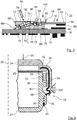
- a radar sensor 10 is shown in different representations.
- the radar sensor 10 can be used, for example, in connection with a driver assistance system of a motor vehicle.
- the radar sensor 10 comprises an openable radar sensor housing 12 in which a ceramic substrate 90 with a radar antenna 14 and a circuit board 16 with components 18 for signal processing and voltage supply are arranged. Furthermore, the radar sensor 10 has a connector 200, which is from the radar sensor housing 12 leads out and can be connected via the corresponding signal lines and power supply lines.
- the radar sensor housing 12 is composed of a basic housing part 22 and a radome 24.
- the basic housing part 22 is made of aluminum, for example.
- the radome 24 is made of plastic, for example PBT.
- the radar sensor housing 12 has approximately the shape of a cuboid.
- the basic housing part 22 and the radome 24 each have the shape of an approximately cuboid trough.
- the radome 24 is placed on an edge of a peripheral wall of the basic housing part 22.
- a circumferential wall 28 of the radome 24 engages around the circumferential wall of the base housing part 22.
- the basic housing part 22 has an installation side 26 with an installation opening.
- the ceramic substrate 90 with the radar antenna 14 and the circuit board 16 can be installed through the installation opening.
- the installation side 26 is openably closed with the radome 24.
- the basic housing part 22, the ceramic substrate 90 with the radar antenna 14, the circuit board 16 and the radome 24 are put together parallel to an imaginary assembly axis 30.
- the radome 24 is fixed to the base housing part 22 by means of a total of four essentially identical clamp connections 32.
- the radome 24 is pressed with the clamp connections 32 parallel to the assembly axis 30 against the edge of the peripheral wall of the base housing part 22.
- the clamp connections 32 are located on opposite longitudinal sides of the radar sensor housing 12. Two of the clamp connections 32 are arranged on the same longitudinal side of the radar sensor housing 12.
- Each clamp connection 32 comprises an elastic clamp element 34 on the side of the radome 24 and a latching lug 36 on the side of the base housing part 22.
- the latching lugs 36 are located on the outer circumferential side of the base housing part 22 and rise radially outward with respect to the assembly axis 30.
- Each of the Latching lugs 36 have a wedge-like bevel 38 on their side facing the installation side 26.
- On the side facing away from the installation side 26, each latching lug 36 has a latching groove 40.
- the clip elements 34 are each elastic spring elements, for example made of spring steel.
- the clamp elements 34 are described below using the clamp element 34 from FIG Figure 4 explained in more detail.
- the clamp element 34 In the area of one of its ends 42, the clamp element 34 has a bend of approximately 90 °. The portion of the clamp element 34 in the region of this bend is embedded in the peripheral wall 28 of the radome 24.
- the clamp element 34 extends in the area of its end 42 in front of the 90 ° bend with respect to the assembly axis 30 radially inward into a cover-side shoulder 48 of the radome 24.
- the clamp element 34 extends on the side of the 90 ° bend facing away from the end 42 roughly parallel to the assembly axis 30.
- the clamp element 34 has an S-shaped bend 44 in its central part running approximately parallel to the assembly axis 30.
- the S-shaped bend 44 is located in an area outside the material of the peripheral wall 28.
- the S-shaped bend 44 is in the assembled state approximately at the level of the wedge-like incline 38 of the corresponding latching lug 36.
- a bent section of the S-shaped bend 44, which faces the peripheral wall 28 of the radome 24, rises towards the peripheral wall of the base housing part 22.
- the clamp element 34 has a latching eye 46 between the S-shaped bend 44 and a free end of the clamp element 34.
- the locking eyelet 46 has the shape of a rectangular window.
- the inner dimensions of the locking lug 46 are somewhat larger than the corresponding outer dimensions of the locking lug 36.
- the locking lug 46 can thus be guided over the locking lug 36 from the outside. In the Figure 4 are indicated by dashed lines for the sake of clarity because of the side boundaries of the locking lug 46 that are actually covered by the locking lug 36.
- the cover-side shoulder 48 forms a rear delimitation of a sealing groove 50, viewed axially to the assembly axis 30 from the radome 24.
- the sealing groove 50 extends circumferentially along the outer circumferential side of the base housing part 22 with respect to the assembly axis 30 and surrounds the installation side 26.
- the sealing groove 50 is delimited at the front by a projection 52 of the base housing part 22.
- the projection 52 extends circumferentially on the outer circumferential side of the base housing part 22 with respect to the assembly axis 30.
- the projection 52 is located between the installation side 26 and the latching lug 36, viewed axially to the assembly axis 30.
- the sealing groove 50 is delimited on its radially inner side with respect to the assembly axis 30 by the peripheral wall of the base housing part 22. On the radially outer side, the sealing groove 50 is delimited by the peripheral wall 28 of the radome 24.
- the circumferential wall 28 overlaps the projection 22.
- the circumferential wall 28 lies with its radially inner circumferential side with respect to the assembly axis 30 on the radially outer circumferential side of the projection 22.
- a seal 54 which is circumferentially connected with respect to the assembly axis 30, is arranged sealingly in the radial direction.
- the radome 24 also has a total of four housing-side clamping elements 56 of a clamping device 58 for clamping the ceramic substrate 90 with the radar antenna 14.
- the housing-side clamping elements 56 are in the Figure 2 , in which the radome 24 is shown transparently for the sake of clarity, and the Figure 3 shown.
- the housing-side clamping elements 56 are arranged on the inner top side of the radome 24 facing the base housing part 22.
- the housing-side clamping elements 56 are each approximately cuboid pedestals which, viewed in the direction of the assembly axis 30, extend away from the top side of the radome 24.
- two of the housing-side clamping elements 56 are located in the area of the same circumferential side of the circumferential wall 28, on which the respective clamp elements 34 are also arranged.
- the clamping elements on the housing side 56 are located approximately between the respective adjacent clamp elements 34.
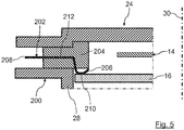
- the connector 200 is located in a circumferential wall 28 of the radome 24 between the clamp connections 32 there.
- the connector 200 comprises several, for example identical, electrical connection elements 202 in the form of elongated bent metal parts, for example bent metal pins.
- the electrical connecting elements 202 are embedded next to one another in a holding element 204 made of plastic.
- the holding element 204 with the connecting elements 202 is for its part embedded in the material of the radome 24.
- the electrical connecting elements 202 thus lead to the outside through the circumferential wall 28 of the radome 24.
- the connecting elements 202 are described below using one shown in FIG Figure 5 Example shown in more detail.
- the connecting element 202 is constructed in one piece overall.
- the connecting element 202 has an inner contact section 206 and an outer contact section 208.
- the inner contact section 206 is located within the radar sensor housing 12 and is used to make electrical contact with a corresponding contact surface 210, for example a conductor track, on the circuit board 16.
- the inner contact section 206 is designed as a surface contact. The contact is made exclusively on the corresponding surfaces of the inner contact section 206 and the corresponding contact area 210.
- the inner contact section 206 is located on the side of the holding element 204 facing the main housing part 22. On the side facing away from the main housing part 22, the inner contact section 206 is supported by a corresponding section of the holding element 204.
- the inner contact section 206 is curved in a convex manner when viewed from the circuit board 16. It is elastically bendable.
- the inner contact section 206 thus has an elastically deformable pre-bend, with which a mechanical preload and a corresponding tolerance compensation can take place in the direction parallel to the assembly axis 30.
- the contact surfaces 210 of the circuit board 16, on which the corresponding inner contact sections 206 of the connecting elements 202 can abut in an electrically conductive manner, are located on the side of the circuit board 16 on which the radar antenna 14 is also arranged.
- the outer contact section 208 is designed as a plug.
- the outer contact section 208 extends outwardly, for example, transversely to the assembly axis 30.
- the outer contact section 208 can be plugged into a corresponding socket on the signal and / or power supply line for electrical connection.
- the electrical connection elements 202 are each embedded with a holding section 212 between the inner contact section 206 and the outer contact section 208 in the holding element 204.
- the holding sections 212 each extend from the outer contact section 208, initially in the same direction, in order to merge into the respective inner contact section 206 after a bend approximately parallel to the assembly axis 30.
- the circuit board 16 is a so-called FR4 circuit card.
- the circuit board 16 is designed as a rectangular flat plate. In a manner which is not of further interest here, it is fastened in the basic housing 22 in such a way that its opposing surfaces each extend perpendicular to the assembly axis 30.
- the components 18 for signal processing and voltage supply are mounted on the surface of the circuit board 16 facing away from the installation side 26 and are electrically connected to corresponding conductor tracks.
- connection device 62 On the surface of the printed circuit board 16 facing the installation side 26, two elongated connection strips 60 of a connection device 62 are arranged.
- the connection device 62 is used for the mechanical and electrical connection of the ceramic substrate 90 to the radar antenna 14.
- the connection strips 60 run as in FIG Figure 2 shown, parallel to one another and each extend between those circumferential sides of the radar sensor housing 12 on which the respective clamp connections 32 are arranged.
- a section of the circuit board 16 with one of the terminal strips 60 is shown in FIG Figure 3 shown in section.
- the connection strips 60 are mechanically connected to the Circuit board 16 and electrically connected to corresponding conductor tracks of circuit board 16.
- connection strips 60 Between the two connection strips 60 is a in the Figure 3
- the absorber element 64 indicated is fastened flatly on the corresponding surface of the circuit board 16, for example glued on.
- the absorber element 64 serves to dampen electromagnetic radiation.
- connection strips 60 The structure of the two connection strips 60 is essentially identical. In the following, the structure is based on the terminal strip 60 from FIG Figure 3 explained in more detail.
- the terminal strip 60 has an electrical contact device 66 for making electrical contact with corresponding electrical contact areas 68 on the side of the ceramic substrate 90 with the radar antenna 14. Furthermore, the terminal strip 60 comprises a connection-side clamping element 70 of the clamping device 58. In addition, the terminal strip 60 has an elongated connection base body 72, on which the connection-side clamping element 70 is realized in one piece and in which a plurality of electrical contact elements 74 of the contact device 66 are mounted.
- connection base body 72 is made of electrically insulating material. It extends between the circumferential sides of the radar sensor housing 12.
- the connection-side clamping element 70 is located on a longitudinal side facing the other connection strip 60 of the connection device 62 Connection body 72.
- a recess 76 is arranged on the side of the connection-side clamping element 70 facing away from the other connection body 72.
- the recess 76 is open on its side facing away from the circuit board 16. It extends almost over the entire length of the connection base body 72.
- a guide gap 78 is located for the electrical contact elements 78.
- the guide gap 78 extends on the one hand Almost over the entire length of the connection base body 72.
- the guide gap 78 connects a rear side of the connection base body 72 facing away from the other connection strip 60 with the recess 76.
- the guide gap 78 opens on the side facing the circuit board 16.
- a pair of holding rods 80 for positioning and mounting the electrical contact elements 74 is arranged in each case.
- the holding rods 80 extend parallel to one another along the connection base body 72.
- the holding rods 80 are made of electrically insulating material.
- a tool holder 82 leads through the upper side of the platform of the connection base body 62 facing away from the printed circuit board 16.
- the tool holder 82 leads into the guide gap 78.
- the tool holder 82 has the shape of an elongated gap which extends beyond the guide gap 78 in the longitudinal direction.
- the tool holder 82 serves to receive and guide an external tool 84 for actuating the contact elements 74.
- the electrical contact device 66 has a multiplicity of electrical contact elements 74 which are arranged next to one another along the connection base body 72 in the guide gap 78.
- the electrical contact elements 74 are not in electrical contact with one another.
- the contact elements 74 of the exemplary embodiment shown are constructed essentially identically.
- Each contact element 74 consists of an elongated elastic electrical conductor, for example a metal spring.
- the contact elements 74 are based on the in Figure 3 contact element 74 shown in more detail.
- the contact element 74 extends through the two openings of the guide gap 78.
- the contact element 74 is mounted between the corresponding holding rods 80 of the two holding rod pairs.
- the contact element 74 is electrically and mechanically connected to a corresponding electrically conductive area of the circuit board 16, for example by means of a soldered connection.
- the contact element 74 is outside the guide gap 78 equipped with a contact arm 86.
- the contact arm 86 merges into two fork-shaped contact fingers 88.
- the contact fingers 88 encompass an edge of the ceramic substrate 90 on opposite sides viewed in the direction of the assembly axis 30.
- the contact element 74 also has an actuating section 92.
- the actuating section 92 is located between the contact arm 86 and the end of the contact element 74 fastened to the printed circuit board 16.
- the actuating section 92 is arranged within the guide gap 78 in the region of the tool holder 82.
- the tool 84 can act on the actuating section 92 and thus move the contact arm 86 from the contact position I into an assembly position II.
- the assembly position II of the contact arm 86 is in the Figure 3 indicated by dashed lines.
- the contact fingers 88 are bent away from the circuit board 16 in the direction of the installation side 26.
- the fork which is formed by the contact fingers 88, is ready to receive the ceramic substrate 90 in the assembly position II.
- the ceramic substrate 90 has, for example, the shape of a rectangular plate.
- the ceramic substrate 90 is formed from a multilayer ceramic such as LTCC.
- the plate surface of the ceramic substrate 90 facing the installation side 26 of the base housing part 22 forms an emission side 94 for the radar antenna 14.
- the ceramic substrate 90 has corresponding antenna structures not shown in detail in the figures.
- a radar TRX chip 96 is arranged on the rear side of the ceramic substrate 90 and is correspondingly electrical contacted.
- the radar TRX chip 96 has a transmitter and a receiver for corresponding radar signals.
- the radar TRX chip 96 is arranged in the free area between the ceramic substrate 90 and the circuit board 16.
- the radar TRX chip 96 is located between the terminal strips 60.
- the basic housing part 22, the radome 24, the connector 200, the printed circuit board 16 with the connection strips 60 and the ceramic substrate 90 with the radar antenna 14 are each preassembled.
- the circuit board 16 with its side carrying the components 18 is first in an assembly direction 98, which in the Figure 3 is indicated by an arrow, installed parallel to the assembly axis 30 in the basic housing part 22 and fixed there.
- One of the tools 84 is then inserted into the tool receptacles 82 of the two connection strips 60.
- the contact elements 74 are thus moved into their assembly position II against their elastic restoring force.
- the ceramic substrate 90 with the radar antenna 14 is placed with the rear side facing away from the emission side 94 first in the assembly direction 98 between the connection strips 60 such that the respective longitudinal edges come to lie in the forks of the contact fingers 88 of the corresponding contact elements 74.
- the tools 84 are removed from the tool receptacles 82, as a result of which the contact elements 74 move into their respective contact position I due to their elastic restoring force.
- respective electrical contacts are established between the contact fingers 88 and the respective contact areas 68 of the ceramic substrate 90.
- the ceramic substrate 90 rests in the correct installation position on the connection-side clamping elements 70, mounted on opposite sides.
- the radome 24 is plugged onto the base housing part 22 in the assembly direction 98 with the seal 54 interposed.
- the corresponding free ends of the clamp elements 34 are each guided over the wedge-like bevels 38 of the latching lugs 36.
- a locking tool 100 which is in the Figure 4 indicated is, the clamp elements 34 are pressed at their S-shaped bends 44 to the peripheral wall of the base housing part 22, whereby the respective locking eyes 46 slide over the locking lugs 36.
- the clamp elements 34 snap into the corresponding locking grooves 40 of the locking lugs 36 due to the elastic restoring force of the clamp elements 34.
- the inner contact sections 206 of the connecting elements 202 of the connector 200 are automatically connected to the corresponding contact surfaces 210 of the circuit board 16 brought into electrical contact.
- the radome 24 is pressed in the direction of the assembly axis 30 against the edge of the base housing part 22.
- the housing-side clamping elements 56 press against the emission side 94 of the ceramic substrate 90.
- the housing-side clamping elements 56 are each located opposite the corresponding connection-side clamping element 70.
- a clamping force is generated in the Figure 3 indicated by an arrow 102, with which the ceramic substrate 90 and thus the radar antenna 14 are clamped between the housing-side clamping elements 56 and the respective connection-side clamping elements 70.
- the inner contact sections 206 of the connector 200 are pressed against the contact surfaces 210 of the circuit board 16 by the clamping force 102.
- the latches of the clamp connection 32 are released with the aid of the locking tool 100.
- the radome 24 is removed from the basic housing part 22 counter to the assembly direction 98.
- the tools 84 are inserted into the respective tool receptacles 82, so that the contact elements 74 are moved into their assembly position II.
- the ceramic substrate 90 with the radar antenna 14 is then removed against the assembly direction 98.
Landscapes
- Engineering & Computer Science (AREA)
- Radar, Positioning & Navigation (AREA)
- Remote Sensing (AREA)
- Physics & Mathematics (AREA)
- Computer Networks & Wireless Communication (AREA)
- General Physics & Mathematics (AREA)
- Electromagnetism (AREA)
- Computer Security & Cryptography (AREA)
- Radar Systems Or Details Thereof (AREA)
- Details Of Aerials (AREA)
Claims (13)
- Capteur radar (10) destiné à un véhicule et comportant au moins un boîtier de capteur radar (12) dans lequel au moins une antenne radar (14) et au moins une carte de circuit imprimé (16) sont disposées, le boîtier de capteur radar (12) comportant au moins une partie de boîtier de base (22) pourvue d'un côté de montage (26) sur lequel l'au moins une antenne radar (14) et l'au moins une carte de circuit imprimé (16) sont montées, et un radôme (24), recouvrant le côté de montage (26) et traversé par des signaux émis par l'au moins une antenne radar (14) et/ou des signaux reçus lorsque le capteur radar (10) est en fonctionnement, le boîtier de capteur radar (12) comportant une pluralité d'éléments de serrage élastiques (34) permettant de fixer le radôme (24) à l'au moins une partie de boîtier de base (22), le radôme (24) comportant au moins un élément de liaison électrique (202) qui comporte à l'intérieur du boîtier de capteur radar (12) au moins une portion de contact intérieure (206) destinée à établir un contact électrique avec l'au moins une carte de circuit imprimé (16) et, à l'extérieur du boîtier de capteur radar (12), au moins une portion de contact extérieure (208) destinée au raccordement d'au moins une ligne électrique, caractérisé en ce qu'au moins une portion de contact intérieure (206) est conçue comme un contact de surface, présente au moins un coude et sert à établir un contact électrique avec une surface de contact correspondante (210) de l'au moins une carte de circuit imprimé (16), et en ce que les éléments de serrage élastiques (34) permettent de réaliser une contrainte de base mécanique avec laquelle l'au moins une portion de contact intérieure (206) est pressée contre l'au moins une surface de contact (210) de l'au moins une carte de circuit imprimé (16).
- Capteur radar selon la revendication 1, caractérisé en ce que l'au moins une portion de contact intérieure (206) est au moins en partie élastique.
- Capteur radar selon la revendication 1 ou 2, caractérisé en ce qu'au moins un élément de liaison électrique (202) est au moins en partie noyé directement ou indirectement dans la matière du radôme (24) .
- Capteur radar selon l'une des revendications précédentes, caractérisé en ce que l'au moins un coude de l'au moins une portion de contact intérieure (206) est situé dans la zone de contact de la surface de contact correspondante (210) de l'au moins une carte de circuit imprimé (16) .
- Capteur radar selon l'une des revendications précédentes, caractérisé en ce que l'au moins un coude de l'au moins une portion de contact intérieure (206) est convexe lorsqu'il est observé depuis l'au moins une carte de circuit imprimé (16).
- Capteur radar selon l'une des revendications précédentes, caractérisé en ce que, lors d'une augmentation de la pression de contact et d'une flexion élastique correspondante de l'au moins une portion de contact intérieure (206), la surface de contact de l'au moins une portion de contact intérieure (206), qui est en appui de manière électriquement conductrice sur une surface de contact correspondante (210) de la carte de circuit imprimé (16), est agrandie.
- Capteur radar selon l'une des revendications précédentes, caractérisé en ce que l'au moins une portion de contact intérieure (206) est dirigée vers la partie de boîtier de base (22).
- Capteur radar selon l'une des revendications précédentes, caractérisé en ce qu'au moins un élément de liaison électrique (202) est disposé au moins en partie dans un élément de retenue (204).
- Capteur radar selon l'une des revendications précédentes, caractérisé en ce qu'au moins un élément de liaison électrique (202) est disposé dans une paroi périphérique (28) du radôme (24) .
- Capteur radar selon l'une des revendications précédentes, caractérisé en ce qu'au moins un élément de liaison électrique (202) est conçu d'une seule pièce avec au moins une portion de contact intérieure (206) et au moins une portion de contact extérieure (208).
- Capteur radar selon l'une des revendications précédentes, caractérisé en ce qu'au moins un élément de liaison électrique (202) à l'extérieur du boîtier de capteur radar (12) est conçu comme une partie d'une connexion électrique rapide (200).
- Capteur radar selon l'une des revendications précédentes, caractérisé en ce que les éléments de serrage élastiques (34) peuvent être utilisés pour réaliser la contrainte de base mécanique avec laquelle l'au moins une carte de circuit imprimé (16) peut également être serrée et fixée.
- Procédé d'assemblage d'un capteur radar (10) destiné à un véhicule et dans lequel au moins une antenne radar (14) et au moins une carte de circuit imprimé (16) sont disposées dans ou sur une partie de boîtier de base (22) d'un boîtier de capteur radar (12) du capteur radar (10), un radôme (24) est monté sur la partie de boîtier de base (22), l'au moins une carte de circuit imprimé (16) étant en contact électrique avec au moins un élément de liaison électrique (202) sur des côtés du radôme (24), et le radôme (24) est fixé à la partie de boîtier de base (22) au moyen d'une pluralité d'éléments de serrage élastiques (34), l'au moins un élément de liaison (202) à l'extérieur du boîtier de capteur radar (12) pouvant être relié à au moins une ligne électrique, caractérisé en ce que, lorsque le radôme (24) est monté sur la partie de boîtier de base (22), une surface de contact (210) de l'au moins une carte de circuit imprimé (16) est en contact électrique avec au moins une portion de contact de surface intérieure (206), qui comporte au moins un coude, d'au moins un élément de liaison électrique (202) sur des côtés du radôme (24), et en ce que des éléments de serrage élastiques (34) réalisent une contrainte de base mécanique avec laquelle l'au moins une portion de contact intérieure (206) est pressée contre l'au moins une surface de contact (210) de l'au moins une carte de circuit imprimé (16) .
Applications Claiming Priority (1)
| Application Number | Priority Date | Filing Date | Title |
|---|---|---|---|
| DE102016123437.0A DE102016123437A1 (de) | 2016-12-05 | 2016-12-05 | Radarsensor für ein Fahrzeug und Verfahren zum Zusammenbau eines Radarsensors |
Publications (2)
| Publication Number | Publication Date |
|---|---|
| EP3330737A1 EP3330737A1 (fr) | 2018-06-06 |
| EP3330737B1 true EP3330737B1 (fr) | 2021-06-30 |
Family
ID=60413079
Family Applications (1)
| Application Number | Title | Priority Date | Filing Date |
|---|---|---|---|
| EP17202560.3A Active EP3330737B1 (fr) | 2016-12-05 | 2017-11-20 | Capteur radar pour un véhicule et procédé d'assemblage d'un capteur radar |
Country Status (2)
| Country | Link |
|---|---|
| EP (1) | EP3330737B1 (fr) |
| DE (1) | DE102016123437A1 (fr) |
Families Citing this family (3)
| Publication number | Priority date | Publication date | Assignee | Title |
|---|---|---|---|---|
| JP7313266B2 (ja) * | 2019-12-18 | 2023-07-24 | ロベルト・ボッシュ・ゲゼルシャフト・ミト・ベシュレンクテル・ハフツング | アダプター、レーダーユニット及び車両 |
| CN113138368B (zh) * | 2020-01-20 | 2025-08-19 | 深圳引望智能技术有限公司 | 一种雷达装置和移动平台 |
| DE102021207850A1 (de) * | 2021-07-22 | 2023-01-26 | Robert Bosch Gesellschaft mit beschränkter Haftung | Sortiment von Radarsensoren |
Citations (2)
| Publication number | Priority date | Publication date | Assignee | Title |
|---|---|---|---|---|
| US2935725A (en) * | 1955-08-30 | 1960-05-03 | Fox Benjamin | Electrical connector for printed circuit board |
| US20060092076A1 (en) * | 2004-10-29 | 2006-05-04 | Franson Steven J | Patch array feed for an automotive radar antenna |
Family Cites Families (2)
| Publication number | Priority date | Publication date | Assignee | Title |
|---|---|---|---|---|
| DE102007042173B4 (de) * | 2007-09-05 | 2019-03-14 | HELLA GmbH & Co. KGaA | Radarsensor |
| DE102012111184A1 (de) | 2012-11-20 | 2014-05-22 | Conti Temic Microelectronic Gmbh | Radareinrichtung für ein Fahrzeug |
-
2016
- 2016-12-05 DE DE102016123437.0A patent/DE102016123437A1/de not_active Withdrawn
-
2017
- 2017-11-20 EP EP17202560.3A patent/EP3330737B1/fr active Active
Patent Citations (2)
| Publication number | Priority date | Publication date | Assignee | Title |
|---|---|---|---|---|
| US2935725A (en) * | 1955-08-30 | 1960-05-03 | Fox Benjamin | Electrical connector for printed circuit board |
| US20060092076A1 (en) * | 2004-10-29 | 2006-05-04 | Franson Steven J | Patch array feed for an automotive radar antenna |
Also Published As
| Publication number | Publication date |
|---|---|
| EP3330737A1 (fr) | 2018-06-06 |
| DE102016123437A1 (de) | 2018-06-07 |
Similar Documents
| Publication | Publication Date | Title |
|---|---|---|
| DE102011013449B4 (de) | Baugruppe mit einem Träger, einem SMD-Bauteil und einem Stanzgitterteil | |
| DE102010037498B4 (de) | Elektrischer Kontakt | |
| EP2034328A1 (fr) | Capteur de radar | |
| EP3330737B1 (fr) | Capteur radar pour un véhicule et procédé d'assemblage d'un capteur radar | |
| EP1282345B1 (fr) | Boîtier abritant une carte électronique avec ses composants dans un véhicule | |
| DE102010039740A1 (de) | Kontaktelement zur Kontaktierung eines Schaltungsträgers, sowie Schaltungsträger mit einem Kontaktelement | |
| DE102014217923A1 (de) | Leiterplattenanordnung, insbesondere für Kfz-Getriebesteuergerät, mit zwei miteinander verbundenen Leiterplatten und einem Spanschutz | |
| EP2787578B1 (fr) | Entraînement de porte comportant un système électrique | |
| EP3728772A1 (fr) | Poignée de portière de véhicule | |
| DE102009009091A1 (de) | Abschirmvorrichtung einer Steckverbindung für ein Fahrzeug und Verfahren zur Herstellung derselben | |
| EP1416614B1 (fr) | Raccord adapter pour un moteur électrique | |
| DE102007033005A1 (de) | Modul und Verfahren zur Herstellung eines Moduls | |
| EP3330733B1 (fr) | Capteur radar pour un véhicule et procédé d'assemblage d'un capteur radar | |
| EP2875552B1 (fr) | Module de commande de véhicule à moteur comportant un élément de connexion, et véhicule comportant un tel module de commande de véhicule à moteur | |
| EP1905121B1 (fr) | Support destine a accueillir un amplificateur d'antenne d'un vehicule | |
| DE102007002193B4 (de) | Mehrteiliges Kontaktierungsbauteil | |
| EP3331100B1 (fr) | Dispositif de raccordement pour un substrat céramique pourvu d'une antenne radar, capteur radar pour un véhicule et procédé de montage d'un capteur radar | |
| EP2609797B1 (fr) | Boîtier destiné à contenir un support de circuit électronique | |
| DE102013219377A1 (de) | Antennenanordnung mit antenneneinheit und verbindereinheit | |
| DE102018113757A1 (de) | Abdeckung für Batteriegehäuse | |
| DE102011086707A1 (de) | Schaltungsanordnung für elektronische und/oder elektrische Bauteile | |
| DE102017129373B4 (de) | Baugruppe, insbesondere Telematikbox für ein Fahrzeug | |
| EP3084895B1 (fr) | Ensemble de liaison et véhicule automobile équipé d'un ensemble de liaison de ce type | |
| DE102016106606B3 (de) | Fahrzeugantenne | |
| DE102025108897A1 (de) | Elektromagnetische abschirmboxbaugruppe und elektromechanische vorrichtung |
Legal Events
| Date | Code | Title | Description |
|---|---|---|---|
| PUAI | Public reference made under article 153(3) epc to a published international application that has entered the european phase |
Free format text: ORIGINAL CODE: 0009012 |
|
| STAA | Information on the status of an ep patent application or granted ep patent |
Free format text: STATUS: THE APPLICATION HAS BEEN PUBLISHED |
|
| AK | Designated contracting states |
Kind code of ref document: A1 Designated state(s): AL AT BE BG CH CY CZ DE DK EE ES FI FR GB GR HR HU IE IS IT LI LT LU LV MC MK MT NL NO PL PT RO RS SE SI SK SM TR |
|
| AX | Request for extension of the european patent |
Extension state: BA ME |
|
| STAA | Information on the status of an ep patent application or granted ep patent |
Free format text: STATUS: REQUEST FOR EXAMINATION WAS MADE |
|
| 17P | Request for examination filed |
Effective date: 20181129 |
|
| RBV | Designated contracting states (corrected) |
Designated state(s): AL AT BE BG CH CY CZ DE DK EE ES FI FR GB GR HR HU IE IS IT LI LT LU LV MC MK MT NL NO PL PT RO RS SE SI SK SM TR |
|
| STAA | Information on the status of an ep patent application or granted ep patent |
Free format text: STATUS: EXAMINATION IS IN PROGRESS |
|
| 17Q | First examination report despatched |
Effective date: 20200420 |
|
| REG | Reference to a national code |
Ref country code: DE Ref legal event code: R079 Ref document number: 502017010774 Country of ref document: DE Free format text: PREVIOUS MAIN CLASS: G01S0013930000 Ipc: G01S0013931000 |
|
| GRAP | Despatch of communication of intention to grant a patent |
Free format text: ORIGINAL CODE: EPIDOSNIGR1 |
|
| STAA | Information on the status of an ep patent application or granted ep patent |
Free format text: STATUS: GRANT OF PATENT IS INTENDED |
|
| RIC1 | Information provided on ipc code assigned before grant |
Ipc: H01Q 1/42 20060101ALI20210119BHEP Ipc: G01S 7/02 20060101ALI20210119BHEP Ipc: H01Q 1/52 20060101ALI20210119BHEP Ipc: H01Q 17/00 20060101ALI20210119BHEP Ipc: G01S 13/931 20200101AFI20210119BHEP Ipc: H01Q 1/32 20060101ALI20210119BHEP |
|
| INTG | Intention to grant announced |
Effective date: 20210208 |
|
| GRAS | Grant fee paid |
Free format text: ORIGINAL CODE: EPIDOSNIGR3 |
|
| GRAA | (expected) grant |
Free format text: ORIGINAL CODE: 0009210 |
|
| STAA | Information on the status of an ep patent application or granted ep patent |
Free format text: STATUS: THE PATENT HAS BEEN GRANTED |
|
| AK | Designated contracting states |
Kind code of ref document: B1 Designated state(s): AL AT BE BG CH CY CZ DE DK EE ES FI FR GB GR HR HU IE IS IT LI LT LU LV MC MK MT NL NO PL PT RO RS SE SI SK SM TR |
|
| REG | Reference to a national code |
Ref country code: CH Ref legal event code: EP |
|
| REG | Reference to a national code |
Ref country code: DE Ref legal event code: R096 Ref document number: 502017010774 Country of ref document: DE Ref country code: AT Ref legal event code: REF Ref document number: 1406843 Country of ref document: AT Kind code of ref document: T Effective date: 20210715 |
|
| REG | Reference to a national code |
Ref country code: IE Ref legal event code: FG4D Free format text: LANGUAGE OF EP DOCUMENT: GERMAN |
|
| REG | Reference to a national code |
Ref country code: LT Ref legal event code: MG9D |
|
| PG25 | Lapsed in a contracting state [announced via postgrant information from national office to epo] |
Ref country code: FI Free format text: LAPSE BECAUSE OF FAILURE TO SUBMIT A TRANSLATION OF THE DESCRIPTION OR TO PAY THE FEE WITHIN THE PRESCRIBED TIME-LIMIT Effective date: 20210630 Ref country code: BG Free format text: LAPSE BECAUSE OF FAILURE TO SUBMIT A TRANSLATION OF THE DESCRIPTION OR TO PAY THE FEE WITHIN THE PRESCRIBED TIME-LIMIT Effective date: 20210930 Ref country code: HR Free format text: LAPSE BECAUSE OF FAILURE TO SUBMIT A TRANSLATION OF THE DESCRIPTION OR TO PAY THE FEE WITHIN THE PRESCRIBED TIME-LIMIT Effective date: 20210630 |
|
| REG | Reference to a national code |
Ref country code: NL Ref legal event code: MP Effective date: 20210630 |
|
| PG25 | Lapsed in a contracting state [announced via postgrant information from national office to epo] |
Ref country code: NO Free format text: LAPSE BECAUSE OF FAILURE TO SUBMIT A TRANSLATION OF THE DESCRIPTION OR TO PAY THE FEE WITHIN THE PRESCRIBED TIME-LIMIT Effective date: 20210930 Ref country code: SE Free format text: LAPSE BECAUSE OF FAILURE TO SUBMIT A TRANSLATION OF THE DESCRIPTION OR TO PAY THE FEE WITHIN THE PRESCRIBED TIME-LIMIT Effective date: 20210630 Ref country code: RS Free format text: LAPSE BECAUSE OF FAILURE TO SUBMIT A TRANSLATION OF THE DESCRIPTION OR TO PAY THE FEE WITHIN THE PRESCRIBED TIME-LIMIT Effective date: 20210630 Ref country code: GR Free format text: LAPSE BECAUSE OF FAILURE TO SUBMIT A TRANSLATION OF THE DESCRIPTION OR TO PAY THE FEE WITHIN THE PRESCRIBED TIME-LIMIT Effective date: 20211001 Ref country code: LV Free format text: LAPSE BECAUSE OF FAILURE TO SUBMIT A TRANSLATION OF THE DESCRIPTION OR TO PAY THE FEE WITHIN THE PRESCRIBED TIME-LIMIT Effective date: 20210630 |
|
| PG25 | Lapsed in a contracting state [announced via postgrant information from national office to epo] |
Ref country code: PT Free format text: LAPSE BECAUSE OF FAILURE TO SUBMIT A TRANSLATION OF THE DESCRIPTION OR TO PAY THE FEE WITHIN THE PRESCRIBED TIME-LIMIT Effective date: 20211102 Ref country code: NL Free format text: LAPSE BECAUSE OF FAILURE TO SUBMIT A TRANSLATION OF THE DESCRIPTION OR TO PAY THE FEE WITHIN THE PRESCRIBED TIME-LIMIT Effective date: 20210630 Ref country code: RO Free format text: LAPSE BECAUSE OF FAILURE TO SUBMIT A TRANSLATION OF THE DESCRIPTION OR TO PAY THE FEE WITHIN THE PRESCRIBED TIME-LIMIT Effective date: 20210630 Ref country code: ES Free format text: LAPSE BECAUSE OF FAILURE TO SUBMIT A TRANSLATION OF THE DESCRIPTION OR TO PAY THE FEE WITHIN THE PRESCRIBED TIME-LIMIT Effective date: 20210630 Ref country code: CZ Free format text: LAPSE BECAUSE OF FAILURE TO SUBMIT A TRANSLATION OF THE DESCRIPTION OR TO PAY THE FEE WITHIN THE PRESCRIBED TIME-LIMIT Effective date: 20210630 Ref country code: EE Free format text: LAPSE BECAUSE OF FAILURE TO SUBMIT A TRANSLATION OF THE DESCRIPTION OR TO PAY THE FEE WITHIN THE PRESCRIBED TIME-LIMIT Effective date: 20210630 Ref country code: SM Free format text: LAPSE BECAUSE OF FAILURE TO SUBMIT A TRANSLATION OF THE DESCRIPTION OR TO PAY THE FEE WITHIN THE PRESCRIBED TIME-LIMIT Effective date: 20210630 Ref country code: SK Free format text: LAPSE BECAUSE OF FAILURE TO SUBMIT A TRANSLATION OF THE DESCRIPTION OR TO PAY THE FEE WITHIN THE PRESCRIBED TIME-LIMIT Effective date: 20210630 |
|
| PG25 | Lapsed in a contracting state [announced via postgrant information from national office to epo] |
Ref country code: PL Free format text: LAPSE BECAUSE OF FAILURE TO SUBMIT A TRANSLATION OF THE DESCRIPTION OR TO PAY THE FEE WITHIN THE PRESCRIBED TIME-LIMIT Effective date: 20210630 |
|
| REG | Reference to a national code |
Ref country code: DE Ref legal event code: R097 Ref document number: 502017010774 Country of ref document: DE |
|
| PG25 | Lapsed in a contracting state [announced via postgrant information from national office to epo] |
Ref country code: DK Free format text: LAPSE BECAUSE OF FAILURE TO SUBMIT A TRANSLATION OF THE DESCRIPTION OR TO PAY THE FEE WITHIN THE PRESCRIBED TIME-LIMIT Effective date: 20210630 |
|
| PLBE | No opposition filed within time limit |
Free format text: ORIGINAL CODE: 0009261 |
|
| STAA | Information on the status of an ep patent application or granted ep patent |
Free format text: STATUS: NO OPPOSITION FILED WITHIN TIME LIMIT |
|
| PG25 | Lapsed in a contracting state [announced via postgrant information from national office to epo] |
Ref country code: AL Free format text: LAPSE BECAUSE OF FAILURE TO SUBMIT A TRANSLATION OF THE DESCRIPTION OR TO PAY THE FEE WITHIN THE PRESCRIBED TIME-LIMIT Effective date: 20210630 |
|
| 26N | No opposition filed |
Effective date: 20220331 |
|
| PG25 | Lapsed in a contracting state [announced via postgrant information from national office to epo] |
Ref country code: MC Free format text: LAPSE BECAUSE OF FAILURE TO SUBMIT A TRANSLATION OF THE DESCRIPTION OR TO PAY THE FEE WITHIN THE PRESCRIBED TIME-LIMIT Effective date: 20210630 |
|
| REG | Reference to a national code |
Ref country code: CH Ref legal event code: PL |
|
| GBPC | Gb: european patent ceased through non-payment of renewal fee |
Effective date: 20211120 |
|
| PG25 | Lapsed in a contracting state [announced via postgrant information from national office to epo] |
Ref country code: LU Free format text: LAPSE BECAUSE OF NON-PAYMENT OF DUE FEES Effective date: 20211120 Ref country code: IT Free format text: LAPSE BECAUSE OF FAILURE TO SUBMIT A TRANSLATION OF THE DESCRIPTION OR TO PAY THE FEE WITHIN THE PRESCRIBED TIME-LIMIT Effective date: 20210630 Ref country code: BE Free format text: LAPSE BECAUSE OF NON-PAYMENT OF DUE FEES Effective date: 20211130 |
|
| REG | Reference to a national code |
Ref country code: BE Ref legal event code: MM Effective date: 20211130 |
|
| PG25 | Lapsed in a contracting state [announced via postgrant information from national office to epo] |
Ref country code: LI Free format text: LAPSE BECAUSE OF NON-PAYMENT OF DUE FEES Effective date: 20211130 Ref country code: CH Free format text: LAPSE BECAUSE OF NON-PAYMENT OF DUE FEES Effective date: 20211130 |
|
| PG25 | Lapsed in a contracting state [announced via postgrant information from national office to epo] |
Ref country code: IE Free format text: LAPSE BECAUSE OF NON-PAYMENT OF DUE FEES Effective date: 20211120 Ref country code: GB Free format text: LAPSE BECAUSE OF NON-PAYMENT OF DUE FEES Effective date: 20211120 |
|
| PG25 | Lapsed in a contracting state [announced via postgrant information from national office to epo] |
Ref country code: LT Free format text: LAPSE BECAUSE OF FAILURE TO SUBMIT A TRANSLATION OF THE DESCRIPTION OR TO PAY THE FEE WITHIN THE PRESCRIBED TIME-LIMIT Effective date: 20210630 |
|
| PG25 | Lapsed in a contracting state [announced via postgrant information from national office to epo] |
Ref country code: HU Free format text: LAPSE BECAUSE OF FAILURE TO SUBMIT A TRANSLATION OF THE DESCRIPTION OR TO PAY THE FEE WITHIN THE PRESCRIBED TIME-LIMIT; INVALID AB INITIO Effective date: 20171120 |
|
| PG25 | Lapsed in a contracting state [announced via postgrant information from national office to epo] |
Ref country code: CY Free format text: LAPSE BECAUSE OF FAILURE TO SUBMIT A TRANSLATION OF THE DESCRIPTION OR TO PAY THE FEE WITHIN THE PRESCRIBED TIME-LIMIT Effective date: 20210630 |
|
| P01 | Opt-out of the competence of the unified patent court (upc) registered |
Effective date: 20230528 |
|
| REG | Reference to a national code |
Ref country code: AT Ref legal event code: MM01 Ref document number: 1406843 Country of ref document: AT Kind code of ref document: T Effective date: 20221120 |
|
| PG25 | Lapsed in a contracting state [announced via postgrant information from national office to epo] |
Ref country code: AT Free format text: LAPSE BECAUSE OF NON-PAYMENT OF DUE FEES Effective date: 20221120 |
|
| PG25 | Lapsed in a contracting state [announced via postgrant information from national office to epo] |
Ref country code: MK Free format text: LAPSE BECAUSE OF FAILURE TO SUBMIT A TRANSLATION OF THE DESCRIPTION OR TO PAY THE FEE WITHIN THE PRESCRIBED TIME-LIMIT Effective date: 20210630 |
|
| PG25 | Lapsed in a contracting state [announced via postgrant information from national office to epo] |
Ref country code: TR Free format text: LAPSE BECAUSE OF FAILURE TO SUBMIT A TRANSLATION OF THE DESCRIPTION OR TO PAY THE FEE WITHIN THE PRESCRIBED TIME-LIMIT Effective date: 20210630 |
|
| PG25 | Lapsed in a contracting state [announced via postgrant information from national office to epo] |
Ref country code: MT Free format text: LAPSE BECAUSE OF FAILURE TO SUBMIT A TRANSLATION OF THE DESCRIPTION OR TO PAY THE FEE WITHIN THE PRESCRIBED TIME-LIMIT Effective date: 20210630 |
|
| PGFP | Annual fee paid to national office [announced via postgrant information from national office to epo] |
Ref country code: DE Payment date: 20251117 Year of fee payment: 9 |
|
| PGFP | Annual fee paid to national office [announced via postgrant information from national office to epo] |
Ref country code: FR Payment date: 20251128 Year of fee payment: 9 |