EP3335228B1 - Conducteur apte à la supraconduction et utilisation du conducteur apte à la supraconduction - Google Patents
Conducteur apte à la supraconduction et utilisation du conducteur apte à la supraconduction Download PDFInfo
- Publication number
- EP3335228B1 EP3335228B1 EP16757151.2A EP16757151A EP3335228B1 EP 3335228 B1 EP3335228 B1 EP 3335228B1 EP 16757151 A EP16757151 A EP 16757151A EP 3335228 B1 EP3335228 B1 EP 3335228B1
- Authority
- EP
- European Patent Office
- Prior art keywords
- superconductor
- tapes
- width
- conductor
- conductive
- Prior art date
- Legal status (The legal status is an assumption and is not a legal conclusion. Google has not performed a legal analysis and makes no representation as to the accuracy of the status listed.)
- Active
Links
Images



Classifications
-
- H—ELECTRICITY
- H01—ELECTRIC ELEMENTS
- H01B—CABLES; CONDUCTORS; INSULATORS; SELECTION OF MATERIALS FOR THEIR CONDUCTIVE, INSULATING OR DIELECTRIC PROPERTIES
- H01B12/00—Superconductive or hyperconductive conductors, cables, or transmission lines
- H01B12/02—Superconductive or hyperconductive conductors, cables, or transmission lines characterised by their form
- H01B12/06—Films or wires on bases or cores
-
- B—PERFORMING OPERATIONS; TRANSPORTING
- B23—MACHINE TOOLS; METAL-WORKING NOT OTHERWISE PROVIDED FOR
- B23K—SOLDERING OR UNSOLDERING; WELDING; CLADDING OR PLATING BY SOLDERING OR WELDING; CUTTING BY APPLYING HEAT LOCALLY, e.g. FLAME CUTTING; WORKING BY LASER BEAM
- B23K1/00—Soldering, e.g. brazing, or unsoldering
- B23K1/19—Soldering, e.g. brazing, or unsoldering taking account of the properties of the materials to be soldered
-
- H—ELECTRICITY
- H01—ELECTRIC ELEMENTS
- H01B—CABLES; CONDUCTORS; INSULATORS; SELECTION OF MATERIALS FOR THEIR CONDUCTIVE, INSULATING OR DIELECTRIC PROPERTIES
- H01B13/00—Apparatus or processes specially adapted for manufacturing conductors or cables
- H01B13/0036—Details
-
- H—ELECTRICITY
- H01—ELECTRIC ELEMENTS
- H01R—ELECTRICALLY-CONDUCTIVE CONNECTIONS; STRUCTURAL ASSOCIATIONS OF A PLURALITY OF MUTUALLY-INSULATED ELECTRICAL CONNECTING ELEMENTS; COUPLING DEVICES; CURRENT COLLECTORS
- H01R4/00—Electrically-conductive connections between two or more conductive members in direct contact, i.e. touching one another; Means for effecting or maintaining such contact; Electrically-conductive connections having two or more spaced connecting locations for conductors and using contact members penetrating insulation
- H01R4/58—Electrically-conductive connections between two or more conductive members in direct contact, i.e. touching one another; Means for effecting or maintaining such contact; Electrically-conductive connections having two or more spaced connecting locations for conductors and using contact members penetrating insulation characterised by the form or material of the contacting members
- H01R4/68—Connections to or between superconductive connectors
-
- H—ELECTRICITY
- H02—GENERATION; CONVERSION OR DISTRIBUTION OF ELECTRIC POWER
- H02G—INSTALLATION OF ELECTRIC CABLES OR LINES, OR OF COMBINED OPTICAL AND ELECTRIC CABLES OR LINES
- H02G15/00—Cable fittings
- H02G15/34—Cable fittings for cryogenic cables
-
- H—ELECTRICITY
- H10—SEMICONDUCTOR DEVICES; ELECTRIC SOLID-STATE DEVICES NOT OTHERWISE PROVIDED FOR
- H10N—ELECTRIC SOLID-STATE DEVICES NOT OTHERWISE PROVIDED FOR
- H10N60/00—Superconducting devices
- H10N60/01—Manufacture or treatment
- H10N60/0268—Manufacture or treatment of devices comprising copper oxide
-
- H—ELECTRICITY
- H10—SEMICONDUCTOR DEVICES; ELECTRIC SOLID-STATE DEVICES NOT OTHERWISE PROVIDED FOR
- H10N—ELECTRIC SOLID-STATE DEVICES NOT OTHERWISE PROVIDED FOR
- H10N60/00—Superconducting devices
- H10N60/20—Permanent superconducting devices
- H10N60/203—Permanent superconducting devices comprising high-Tc ceramic materials
-
- Y—GENERAL TAGGING OF NEW TECHNOLOGICAL DEVELOPMENTS; GENERAL TAGGING OF CROSS-SECTIONAL TECHNOLOGIES SPANNING OVER SEVERAL SECTIONS OF THE IPC; TECHNICAL SUBJECTS COVERED BY FORMER USPC CROSS-REFERENCE ART COLLECTIONS [XRACs] AND DIGESTS
- Y02—TECHNOLOGIES OR APPLICATIONS FOR MITIGATION OR ADAPTATION AGAINST CLIMATE CHANGE
- Y02E—REDUCTION OF GREENHOUSE GAS [GHG] EMISSIONS, RELATED TO ENERGY GENERATION, TRANSMISSION OR DISTRIBUTION
- Y02E40/00—Technologies for an efficient electrical power generation, transmission or distribution
- Y02E40/60—Superconducting electric elements or equipment; Power systems integrating superconducting elements or equipment
Definitions
- the conductors When transmitting high electrical power through superconductors, the conductors have to be cooled accordingly. In this respect, it is desirable to keep the volume to be cooled as small as possible, ie to achieve high current densities in the bundle or cable. A high power density is also desired when generating high fields in large magnets. At the same time, the cables must have high mechanical stability, e.g. with regard to mechanical support with the lowest possible heat input, thermal cycles or electromagnetic forces.
- the pamphlet JP H09 223418 A discloses an oxide superconducting wire and a method of making the same.
- the superconducting wire comprises a multitude of BSCCO superconductors embedded in a silver matrix.
- the pamphlet US2010/099570A1 discloses a superconductor cable having a plurality of flat superconductor tapes joined together to form a stack with a rectangular cross-section, the stack having a twist about a longitudinal axis of the stack.
- the pamphlet U.S. 6,271,474 B1 discloses a wire comprising an oxide superconducting material and a silver or silver alloy stabilizer matrix covering the oxide superconducting material.
- a conductive or electrically conductive band is generally understood to mean a flat, electrically conductive band which, for example, has a thickness of approximately 100 ⁇ m and, for example, a width of approximately 2 mm to 12 mm.
- the length of a conductive tape can be e.g. 1 m to 1 km or even more.
- a conductive tape can in particular be a metal tape such as a copper tape.
- the conductive band can be formed partially or entirely of metal such as copper.
- a conductive strip can also be superconductive.
- a conductive tape can be a superconductor tape.
- the superconductive conductor comprises a plurality of first conductive bands and a plurality of second conductive bands, each first conductive band differing in width from a second conductive band.
- Each of the first conductive bands has the same width, namely a first width.
- the superconductive conductor comprises a multiplicity of first superconductor tapes and a multiplicity of second superconductor tapes, with a first superconductor tape differing in width from a second superconductor tape in each case.
- Each of the first superconductor tapes has the same width, namely a first width.
- each of the second superconductor tapes also has the same width, namely a second width that differs from the first width.
- the width of a conductive tape or superconductor tape is understood to be the distance between opposite end or longitudinal edges of the tape, with the end or longitudinal edges extending along the tape, ie corresponding to the long edges of the tape.
- the width of the conductive tape or superconductor tape is always smaller than the length of the conductive tape or superconductor tape.
- the thickness of the superconductor tape is understood to mean the dimension of the superconductor tape in the direction of the substrate-superconductor transition.
- the electrical conductor preferably comprises only first and second conductive tapes, in particular superconductor tapes, i.e. conductive tapes or superconductor tapes with the first width and conductive tapes or superconductor tapes with the second width.
- the electrical conductor preferably does not include any conductive tapes or superconductor tapes with widths other than the first and second widths.
- the first width is greater than the second width.
- the first width can be about 6 mm and the second width can be about 4 mm.
- the superconductor body or the electrical conductor is also referred to as a cross conductor or cross-conductor or CroCo for short within the meaning of the invention.
- the outer circular cross-section of a round conductor can advantageously be produced better than in previously realized superconductor stacks.
- the crossover conductor can be manufactured in a simple manner.
- the cross-shape improves the use of the cross-section in comparison to a tape stack which only has conductive tapes or superconductor tapes with only one width. As a result, the current density through the conductor can advantageously be increased.
- the first and second widths of the conductive tapes or superconductor tapes are preferably selected in such a way that the ratio of the first width b 1 to the second width b 2 is: 0.6 ⁇ b 2 / b 1 ⁇ 0.7
- middle section is arranged directly between the two end sections means that the end sections each border seamlessly, i.e. without any further intermediate sections, on the middle section.
- the tape stack or the superconductor body does not include any sections other than the middle section and the two end sections.
- the middle section has a large number, for example twenty, first conductive strips or superconductor strips and each of the two end sections has a large number, for example five, second conductive strips or superconductor strips. It goes without saying that the respective number of first and second conductive strips or superconductor strips can be selected depending on the application and/or the desired shape of the electrical conductor.
- the cross conductor according to the invention which has exactly two different conductive strips or superconductor strips each with exactly two different widths, on the other hand ensures a high cross-section utilization with good twistability at the same time and a significantly lower production outlay.
- the cladding tube can also be made of stainless steel or similar materials. This gives the superconductive conductor a special stability.
- the superconductive conductor preferably comprises one or more steel wires. If the superconductor body is wrapped with steel strips, the conductivity between the superconductor body and the cladding tube can be reduced.
- the tape stack or the superconductor body has a twist.
- the conductive tapes or superconductor tapes stacked on top of one another are twisted together.
- the superconducting conductor according to the invention can be used to transmit large currents, e.g. in the range from 10 kA to 100 kA or more, e.g. from a power plant to an aluminum smelter, when connecting a wind farm to the power grid or for long-distance transmission of high electrical power, especially in Areas where local overhead lines are unsuitable. Due to the high currents or the high current densities that can flow in the superconductive conductor according to the invention, the superconductive conductor according to the invention can be used to generate high magnetic fields, for example for particle accelerators.
- the superconductive conductor of the present invention can be used to form a cable suitable for power transmission and/or high magnetic field generation.
- a number of conductors adapted to the current to be transmitted can be arranged around a central tube or a suitable holder, so that the stray field of the individual conductors is minimized.
- coolant can be pumped through the tube to cool the superconductors.
- the superconducting conductor according to the invention can also be used to form a bent cable are used by the superconductive conductor for bending the superconductive conductor is locally heated, in particular to or above the melting temperature of the solder or solder used in the superconductive conductor. In the heated state, the solder advantageously allows a local displacement of the conductive strips or superconductor strips among one another.
- the position information chosen in the present description are each related to the directly described and illustrated figure and are to be transferred to the new position in the event of a change of position.
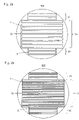
- Figures 2a and 2b each show a schematic image of the cross section of a superconducting conductor 100 according to the invention
- Figures 2a and 2b differ only in the number of conductive tapes or superconductor tapes used.
- the tape stack 30 can be divided into three sections, namely a middle section 10 and two end sections 20.
- the middle section 10, which is arranged between the two end sections 20, comprises in the embodiment shown Figures 2a and 2b exclusively first superconductor tapes 1 and the two end sections 20 exclusively comprise second superconductor tapes 2.
- the cross conductor according to the invention thus has superconductor tapes, in particular REBCO tapes, with two different cross sections or widths.
- superconductor tapes in particular REBCO tapes
- the circular cross-section of a round conductor can be better utilized than in previously realized superconductor stacks and at the same time a simple manufacture is made possible.
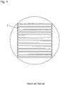
- the use of a cross-shaped superconductor tape stack instead of a square superconductor tape stack brings about a significant improvement in cross-sectional utilization.
- the geometric Fill factor for the square stack from the figure 1 is only 63.6%
- the geometric fill factor in the case of the cross-section tape stack is 78.4% (calculated for a first width of 6 mm and a second width of 4 mm).
- the significantly better use of the cross-section means that the current-carrying capacity and current density of the conductor can also be increased.
- the geometric fill factor can be further increased by using superconductor tapes with more than two different widths and producing a tape stack whose cross section has a multi-step shape rather than a cross.
- a multi-stage form can be disadvantageous, in particular with regard to the ability of the conductor to be twisted. Rather, it has surprisingly turned out within the scope of the invention that it is advantageous to use only superconductor tapes with exactly two different widths for the tape stack, in order to thus realize a cross-shaped cross section of the tape stack.
- a total of 30 to 36 tapes each having a thickness of about 150 to 165 microns, can be used for the tape stack.
- Two thirds (ie 20 to 24) of the bands are preferably 6 mm wide and one third of the bands (ie 10 to 12) are 4 mm wide. Taking into account the thickness of the solder layers between the individual strips, this results in a thickness of the crossed conductor of around 5.5 mm to 6.2 mm, i.e. an almost four-fold symmetry in the external shape.
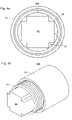
- the Figures 4a and 4b 12 each show a schematic image of the cross-section of a superconductive conductor 100 according to the invention according to a preferred embodiment, before the conductor has been compacted.
- the cross-shaped tape stack or the individual superconductor tapes of the tape stack were soldered to form a superconductor body 40 and inserted into a round cladding tube 50 , with a soldering wire 45 being wrapped around the superconductor body 40 before it was inserted into the cladding tube 50 .
- the Figures 5a and 5b each show a schematic image of the superconductive conductor 100 after it has been heated above the melting temperature of the soldering strip 45 and compacted using suitable methods, such as rotary swaging and/or drawing. Like in the Figure 5a and the perspective view of Figure 5b can be seen is from the solder wire 45 of Figure 4a or 4b has become an extended layer of solder 47 between the superconductor body 40 and the cladding tube 50 as a result of the heating and/or compacting.
- the Figures 6a, 6b , 7a and 7b correspond to the Figures 4a, 4b , 5a and 5b except that the superconductive conductor 100 in the embodiment of FIG Figures 6a, 6b , 7a and 7b additional shaped pieces 60 which are arranged together with the superconductor body 40 in the cladding tube 50 or inserted into the cladding tube 50 . In this way, stability can be increased and solder can be saved.
- the superconductor body 40 can be wrapped with other or further wires or tapes, e.g. with metal wires made of copper, aluminum and/or brass, or with steel wires. Such additional wires can ensure or increase the stability and/or the conductivity, in particular in the event of a quench.
- the Figures 8a to 8d show schematic images of different arrangements of one or more superconducting conductors 100 according to the invention for forming a composite or cable.
- the cross conductor according to the invention 100 can, as in the Figure 8a shown singly or, as in the Figures 8b to 8d shown, are used as cables, especially in twisted networks, in order to increase the current-carrying capacity depending on the application.
- a cable 103 with three superconductive conductors 100 twisted together is shown in FIG Figure 8c
- a cable 105 with five superconducting conductors 100 twisted together is shown
- a cable 124 having 24 superconductive conductors 100 twisted together is shown.
- a number of conductors 100 adapted to the current to be transmitted can be arranged around a central tube 70 or a suitable holder, so that the stray field of the individual conductors 100 is minimized. Coolant can be pumped through tube 70 to cool the superconductors.
- cable 150 shown has a protective sheath 80, which is preferably electrically insulating.
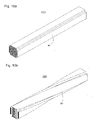
- FIG. 12 shows a schematic drawing of a superconductive conductor 100 without twist
- FIG Figure 10b a schematic drawing of a superconducting conductor 100 with twists is shown.
- the superconducting conductor 100 according to the invention also has good current distribution and short current coupling lengths due to the uniform and reliable soldering of the superconductor strips or the strip stack in the soldering bath. Stress and tensile tests carried out at a temperature of 4.2 K and a magnetic field of 12 T showed that the cross-conductor according to the invention only begins to degrade at stress values that are comparable to those of the individual superconductor tapes.
Landscapes
- Engineering & Computer Science (AREA)
- Chemical & Material Sciences (AREA)
- Manufacturing & Machinery (AREA)
- Physics & Mathematics (AREA)
- Condensed Matter Physics & Semiconductors (AREA)
- General Physics & Mathematics (AREA)
- Materials Engineering (AREA)
- Mechanical Engineering (AREA)
- Ceramic Engineering (AREA)
- Superconductors And Manufacturing Methods Therefor (AREA)
Claims (9)
- Un conducteur supraconducteur (100) comprenant :- une pluralité de premières bandes conductrices (1), chacune présentant une première largeur ; et- une pluralité de deuxièmes bandes conductrices (2), chacune présentant une deuxième largeur ;sachant que la première largeur est différente de la deuxième largeur,sachant que la pluralité de premières bandes conductrices (1) et/ou la pluralité de deuxièmes bandes conductrices (2) comprend au moins une bande supraconductrice,sachant que la pluralité de premières bandes conductrices (1) et la pluralité de deuxièmes bandes conductrices (2) sont agencées en un empilement de bandes (30) présentant une section transversale en forme de croix, etsachant que respectivement deux bandes conductrices se succédant dans l'empilement de bandes (30) étant soudées entre elles, de manière qu'un corps supraconducteur (40) est formé à partir de l'empilement de bandes (30).
- Le conducteur supraconducteur (100) d'après la revendication 1, sachant que l'empilement de bandes (30) est constitué uniquement de bandes de deux largeurs différentes.
- Le conducteur supraconducteur (100) d'après la revendication 1 ou 2, sachant que l'empilement de bandes (30) comprend uniquement des premières bandes conductrices (1) de la première largeur et des deuxièmes bandes conductrices (2) de la deuxième largeur.
- Le conducteur supraconducteur (100) d'après la revendication 1, sachant que l'empilement de bandes (30) est constitué d'une portion centrale (10) et de deux portions d'extrémité (20), sachant que la portion centrale (10) est agencée directement entre les deux portions d'extrémité (20), et sachant que la portion centrale (10) comprend uniquement des premières bandes conductrices (1) et que les portions d'extrémité (20) comprennent chacune uniquement des deuxièmes bandes conductrices (2).
- Le conducteur supraconducteur (100) d'après l'une quelconque des revendications précédentes, comprenant en outre :- un tube de gainage (50) et/ou- une ou plusieurs pièces façonnées conductrices (60) et/ou- un ou plusieurs fils métalliques et/ou- un ou plusieurs fils d'acier et/ou- un matériau isolant.
- Le conducteur supraconducteur (100) d'après l'une quelconque des revendications précédentes, sachant que le corps supraconducteur (40) présente un torsadage.
- Une utilisation du conducteur supraconducteur (100) d'après l'une quelconque des revendications précédentes pour la transmission d'énergie ou la génération de champs magnétiques ou pour former un câble (103 ; 105 ; 124 ; 150) apte à la transmission d'énergie et/ou à la génération de champs magnétiques.
- L'utilisation d'après la revendication 7, sachant que le conducteur supraconducteur (100) est utilisé pour former un câble (103 ; 105 ; 124 ; 150) et que le câble (103 ; 105 ; 124 ; 150) est constitué d'une pluralité des conducteurs supraconducteurs (100), notamment d'un ou plusieurs ensembles torsadés des conducteurs supraconducteurs (100).
- L'utilisation d'après la revendication 7 ou 8, sachant que le conducteur supraconducteur (100) est chauffé localement, notamment à ou au-dessus de la température de fusion du matériau d'apport de soudure utilisé dans le conducteur supraconducteur (100), pour former un câble courbé.
Applications Claiming Priority (2)
| Application Number | Priority Date | Filing Date | Title |
|---|---|---|---|
| DE102015010636.8A DE102015010636A1 (de) | 2015-08-12 | 2015-08-12 | Supraleitfähiger Leiter und Verwendung des supraleitfähigen Leiters |
| PCT/EP2016/001368 WO2017025189A1 (fr) | 2015-08-12 | 2016-08-10 | Conducteur apte à la supraconduction et utilisation du conducteur apte à la supraconduction |
Publications (2)
| Publication Number | Publication Date |
|---|---|
| EP3335228A1 EP3335228A1 (fr) | 2018-06-20 |
| EP3335228B1 true EP3335228B1 (fr) | 2022-07-13 |
Family
ID=56801492
Family Applications (1)
| Application Number | Title | Priority Date | Filing Date |
|---|---|---|---|
| EP16757151.2A Active EP3335228B1 (fr) | 2015-08-12 | 2016-08-10 | Conducteur apte à la supraconduction et utilisation du conducteur apte à la supraconduction |
Country Status (5)
| Country | Link |
|---|---|
| US (1) | US10825585B2 (fr) |
| EP (1) | EP3335228B1 (fr) |
| CN (1) | CN108140458B (fr) |
| DE (1) | DE102015010636A1 (fr) |
| WO (1) | WO2017025189A1 (fr) |
Families Citing this family (2)
| Publication number | Priority date | Publication date | Assignee | Title |
|---|---|---|---|---|
| EP3635754B1 (fr) * | 2017-06-09 | 2024-11-27 | Brookhaven Technology Group, Inc. | Câble supraconducteur flexible à haute température à filaments multiples |
| CN110752063B (zh) * | 2018-07-24 | 2022-08-19 | 中国电力科学研究院有限公司 | 一种含内外超导层的高温超导复合导体 |
Citations (4)
| Publication number | Priority date | Publication date | Assignee | Title |
|---|---|---|---|---|
| JPH09223418A (ja) * | 1996-02-19 | 1997-08-26 | Mitsubishi Electric Corp | 酸化物超電導線材及びその製造方法 |
| US5929000A (en) * | 1996-03-26 | 1999-07-27 | Sumitomo Electric Industries, Ltd. | Multifilamentary oxide superconducting wires |
| US6271474B1 (en) * | 1997-11-14 | 2001-08-07 | Sumitomo Electric Industries, Ltd. | Methods of manufacturing oxide superconducting stranded wire and oxide superconducting cable conductor, and coated wire, stranded wire and cable conductor |
| US20100099570A1 (en) * | 2008-10-08 | 2010-04-22 | Makoto Takayasu | Superconductor cable |
Family Cites Families (13)
| Publication number | Priority date | Publication date | Assignee | Title |
|---|---|---|---|---|
| US2288855A (en) * | 1940-06-07 | 1942-07-07 | Line Material Co | Method and means for making cores for transformers or the like |
| US2431155A (en) * | 1943-08-20 | 1947-11-18 | Line Material Co | Three-phase transformer and method of making the same |
| US2498747A (en) * | 1944-09-20 | 1950-02-28 | Mcgraw Electric Co | Electromagnetic device and method of making the same |
| US3137832A (en) * | 1960-12-27 | 1964-06-16 | Gen Electric | Laminated magnetic core structure |
| US3333220A (en) * | 1966-01-28 | 1967-07-25 | Westinghouse Electric Corp | Corona shielding means for magnetic cores |
| US3708606A (en) * | 1970-05-13 | 1973-01-02 | Air Reduction | Cryogenic system including variations of hollow superconducting wire |
| US4994633A (en) * | 1988-12-22 | 1991-02-19 | General Atomics | Bend-tolerant superconductor cable |
| JP3165000B2 (ja) * | 1995-04-21 | 2001-05-14 | 株式会社日立製作所 | 内燃機関用点火装置 |
| JP3657397B2 (ja) * | 1997-07-16 | 2005-06-08 | 住友電気工業株式会社 | 酸化物超電導線材およびその製造方法 |
| US6256521B1 (en) * | 1997-09-16 | 2001-07-03 | Ut-Battelle, Llc | Preferentially oriented, High temperature superconductors by seeding and a method for their preparation |
| AT406923B (de) * | 1998-02-24 | 2000-10-25 | Asta Elektrodraht Gmbh | Mehrfachparallelleiter für elektrische maschinen und geräte |
| US6621966B2 (en) * | 1999-03-31 | 2003-09-16 | Corning Cable Systems Llc | Fiber optic cable with profiled group of optical fibers |
| DE102006019296A1 (de) * | 2006-04-26 | 2007-10-31 | Robert Bosch Gmbh | Zündspule, insbesondere für eine Brennkraftmaschine eines Kraftfahrzeugs |
-
2015
- 2015-08-12 DE DE102015010636.8A patent/DE102015010636A1/de not_active Withdrawn
-
2016
- 2016-08-10 WO PCT/EP2016/001368 patent/WO2017025189A1/fr not_active Ceased
- 2016-08-10 US US15/752,235 patent/US10825585B2/en active Active
- 2016-08-10 CN CN201680059630.3A patent/CN108140458B/zh active Active
- 2016-08-10 EP EP16757151.2A patent/EP3335228B1/fr active Active
Patent Citations (4)
| Publication number | Priority date | Publication date | Assignee | Title |
|---|---|---|---|---|
| JPH09223418A (ja) * | 1996-02-19 | 1997-08-26 | Mitsubishi Electric Corp | 酸化物超電導線材及びその製造方法 |
| US5929000A (en) * | 1996-03-26 | 1999-07-27 | Sumitomo Electric Industries, Ltd. | Multifilamentary oxide superconducting wires |
| US6271474B1 (en) * | 1997-11-14 | 2001-08-07 | Sumitomo Electric Industries, Ltd. | Methods of manufacturing oxide superconducting stranded wire and oxide superconducting cable conductor, and coated wire, stranded wire and cable conductor |
| US20100099570A1 (en) * | 2008-10-08 | 2010-04-22 | Makoto Takayasu | Superconductor cable |
Also Published As
| Publication number | Publication date |
|---|---|
| WO2017025189A1 (fr) | 2017-02-16 |
| US10825585B2 (en) | 2020-11-03 |
| US20180226178A1 (en) | 2018-08-09 |
| CN108140458B (zh) | 2020-07-07 |
| CN108140458A (zh) | 2018-06-08 |
| DE102015010636A1 (de) | 2017-02-16 |
| EP3335228A1 (fr) | 2018-06-20 |
Similar Documents
| Publication | Publication Date | Title |
|---|---|---|
| DE69405678T2 (de) | Supraleitender Kabelleiter | |
| CH616775A5 (fr) | ||
| EP2717340B1 (fr) | Fil semi-fini pour un fil supraconducteur Nb3Sn | |
| DE69621183T2 (de) | Draht aus supraleitendem Oxid und Verfahren zu dessen Herstellung | |
| DE69427439T2 (de) | Draht aus supraleitendem Oxid, Verfahren zur Herstellung, Spule und Kabel aus supraleitendem Oxid | |
| DE2749052C2 (fr) | ||
| DE69422746T2 (de) | Hochtemperatur-supraleitender Kabelleiter aus oxidischem Supraleiter | |
| EP2017856B1 (fr) | Câble électrique résistant à une forte conduction | |
| DE2736157C3 (fr) | ||
| DE69202275T3 (de) | Verbindung zwischen Drähten unter Verwendung von Oxid-Supraleitern und Methode für die Verbindung. | |
| DE69714646T2 (de) | Verbindungsstruktur für ein Supraleiter | |
| DE3045277C2 (de) | Supraleiter | |
| EP1589542A1 (fr) | Câble supraconducteur et son procédé de fabrication | |
| EP3317903B1 (fr) | Procédé et dispositif de fabrication d'un conducteur supraconducteur | |
| EP3335228B1 (fr) | Conducteur apte à la supraconduction et utilisation du conducteur apte à la supraconduction | |
| DE3048418C2 (de) | Kabelförmiger, kryogen stabilisierter Supraleiter für hohe Ströme und Wechselfeldbelastungen | |
| EP2634779A1 (fr) | Système doté d'un élément de transmission électrique supraconducteur triphasé | |
| DE69601875T2 (de) | Elektrische leiter und kabel | |
| DE19719738B4 (de) | AC-Oxid-Supraleiterkabel und Verfahren zur Herstellung eines AC-Oxid-Supraleiterbanddrahtes und eines AC-Oxid-Supraleiterrunddrahts | |
| DE2218223C2 (de) | Verbundleiter und Verfahren zu dessen Herstellung | |
| DE10249550A1 (de) | Supraleitender Kabelleiter mit SEBCO-beschichteten Leiterelementen | |
| EP0311650B1 (fr) | Procede de fabrication d'un element supraconducteur | |
| DE3803285C2 (fr) | ||
| DE2907083C2 (de) | Supraleitende Magnetwicklung mit mehrren Wicklungslagen | |
| DE69508208T2 (de) | Draht aus supraleitender Verbindung |
Legal Events
| Date | Code | Title | Description |
|---|---|---|---|
| STAA | Information on the status of an ep patent application or granted ep patent |
Free format text: STATUS: THE INTERNATIONAL PUBLICATION HAS BEEN MADE |
|
| PUAI | Public reference made under article 153(3) epc to a published international application that has entered the european phase |
Free format text: ORIGINAL CODE: 0009012 |
|
| STAA | Information on the status of an ep patent application or granted ep patent |
Free format text: STATUS: REQUEST FOR EXAMINATION WAS MADE |
|
| 17P | Request for examination filed |
Effective date: 20180111 |
|
| AK | Designated contracting states |
Kind code of ref document: A1 Designated state(s): AL AT BE BG CH CY CZ DE DK EE ES FI FR GB GR HR HU IE IS IT LI LT LU LV MC MK MT NL NO PL PT RO RS SE SI SK SM TR |
|
| AX | Request for extension of the european patent |
Extension state: BA ME |
|
| DAV | Request for validation of the european patent (deleted) | ||
| DAX | Request for extension of the european patent (deleted) | ||
| STAA | Information on the status of an ep patent application or granted ep patent |
Free format text: STATUS: EXAMINATION IS IN PROGRESS |
|
| 17Q | First examination report despatched |
Effective date: 20190222 |
|
| GRAP | Despatch of communication of intention to grant a patent |
Free format text: ORIGINAL CODE: EPIDOSNIGR1 |
|
| STAA | Information on the status of an ep patent application or granted ep patent |
Free format text: STATUS: GRANT OF PATENT IS INTENDED |
|
| INTG | Intention to grant announced |
Effective date: 20220214 |
|
| GRAS | Grant fee paid |
Free format text: ORIGINAL CODE: EPIDOSNIGR3 |
|
| GRAA | (expected) grant |
Free format text: ORIGINAL CODE: 0009210 |
|
| STAA | Information on the status of an ep patent application or granted ep patent |
Free format text: STATUS: THE PATENT HAS BEEN GRANTED |
|
| AK | Designated contracting states |
Kind code of ref document: B1 Designated state(s): AL AT BE BG CH CY CZ DE DK EE ES FI FR GB GR HR HU IE IS IT LI LT LU LV MC MK MT NL NO PL PT RO RS SE SI SK SM TR |
|
| REG | Reference to a national code |
Ref country code: CH Ref legal event code: EP |
|
| REG | Reference to a national code |
Ref country code: IE Ref legal event code: FG4D Free format text: LANGUAGE OF EP DOCUMENT: GERMAN |
|
| REG | Reference to a national code |
Ref country code: DE Ref legal event code: R096 Ref document number: 502016015070 Country of ref document: DE |
|
| REG | Reference to a national code |
Ref country code: AT Ref legal event code: REF Ref document number: 1504691 Country of ref document: AT Kind code of ref document: T Effective date: 20220815 |
|
| REG | Reference to a national code |
Ref country code: LT Ref legal event code: MG9D |
|
| REG | Reference to a national code |
Ref country code: NL Ref legal event code: MP Effective date: 20220713 |
|
| PG25 | Lapsed in a contracting state [announced via postgrant information from national office to epo] |
Ref country code: SE Free format text: LAPSE BECAUSE OF FAILURE TO SUBMIT A TRANSLATION OF THE DESCRIPTION OR TO PAY THE FEE WITHIN THE PRESCRIBED TIME-LIMIT Effective date: 20220713 Ref country code: RS Free format text: LAPSE BECAUSE OF FAILURE TO SUBMIT A TRANSLATION OF THE DESCRIPTION OR TO PAY THE FEE WITHIN THE PRESCRIBED TIME-LIMIT Effective date: 20220713 Ref country code: PT Free format text: LAPSE BECAUSE OF FAILURE TO SUBMIT A TRANSLATION OF THE DESCRIPTION OR TO PAY THE FEE WITHIN THE PRESCRIBED TIME-LIMIT Effective date: 20221114 Ref country code: NO Free format text: LAPSE BECAUSE OF FAILURE TO SUBMIT A TRANSLATION OF THE DESCRIPTION OR TO PAY THE FEE WITHIN THE PRESCRIBED TIME-LIMIT Effective date: 20221013 Ref country code: NL Free format text: LAPSE BECAUSE OF FAILURE TO SUBMIT A TRANSLATION OF THE DESCRIPTION OR TO PAY THE FEE WITHIN THE PRESCRIBED TIME-LIMIT Effective date: 20220713 Ref country code: LV Free format text: LAPSE BECAUSE OF FAILURE TO SUBMIT A TRANSLATION OF THE DESCRIPTION OR TO PAY THE FEE WITHIN THE PRESCRIBED TIME-LIMIT Effective date: 20220713 Ref country code: LT Free format text: LAPSE BECAUSE OF FAILURE TO SUBMIT A TRANSLATION OF THE DESCRIPTION OR TO PAY THE FEE WITHIN THE PRESCRIBED TIME-LIMIT Effective date: 20220713 Ref country code: FI Free format text: LAPSE BECAUSE OF FAILURE TO SUBMIT A TRANSLATION OF THE DESCRIPTION OR TO PAY THE FEE WITHIN THE PRESCRIBED TIME-LIMIT Effective date: 20220713 Ref country code: ES Free format text: LAPSE BECAUSE OF FAILURE TO SUBMIT A TRANSLATION OF THE DESCRIPTION OR TO PAY THE FEE WITHIN THE PRESCRIBED TIME-LIMIT Effective date: 20220713 |
|
| PG25 | Lapsed in a contracting state [announced via postgrant information from national office to epo] |
Ref country code: PL Free format text: LAPSE BECAUSE OF FAILURE TO SUBMIT A TRANSLATION OF THE DESCRIPTION OR TO PAY THE FEE WITHIN THE PRESCRIBED TIME-LIMIT Effective date: 20220713 Ref country code: IS Free format text: LAPSE BECAUSE OF FAILURE TO SUBMIT A TRANSLATION OF THE DESCRIPTION OR TO PAY THE FEE WITHIN THE PRESCRIBED TIME-LIMIT Effective date: 20221113 Ref country code: HR Free format text: LAPSE BECAUSE OF FAILURE TO SUBMIT A TRANSLATION OF THE DESCRIPTION OR TO PAY THE FEE WITHIN THE PRESCRIBED TIME-LIMIT Effective date: 20220713 Ref country code: GR Free format text: LAPSE BECAUSE OF FAILURE TO SUBMIT A TRANSLATION OF THE DESCRIPTION OR TO PAY THE FEE WITHIN THE PRESCRIBED TIME-LIMIT Effective date: 20221014 |
|
| REG | Reference to a national code |
Ref country code: DE Ref legal event code: R097 Ref document number: 502016015070 Country of ref document: DE |
|
| PG25 | Lapsed in a contracting state [announced via postgrant information from national office to epo] |
Ref country code: SM Free format text: LAPSE BECAUSE OF FAILURE TO SUBMIT A TRANSLATION OF THE DESCRIPTION OR TO PAY THE FEE WITHIN THE PRESCRIBED TIME-LIMIT Effective date: 20220713 Ref country code: RO Free format text: LAPSE BECAUSE OF FAILURE TO SUBMIT A TRANSLATION OF THE DESCRIPTION OR TO PAY THE FEE WITHIN THE PRESCRIBED TIME-LIMIT Effective date: 20220713 Ref country code: MC Free format text: LAPSE BECAUSE OF FAILURE TO SUBMIT A TRANSLATION OF THE DESCRIPTION OR TO PAY THE FEE WITHIN THE PRESCRIBED TIME-LIMIT Effective date: 20220713 Ref country code: LU Free format text: LAPSE BECAUSE OF NON-PAYMENT OF DUE FEES Effective date: 20220810 Ref country code: DK Free format text: LAPSE BECAUSE OF FAILURE TO SUBMIT A TRANSLATION OF THE DESCRIPTION OR TO PAY THE FEE WITHIN THE PRESCRIBED TIME-LIMIT Effective date: 20220713 Ref country code: CZ Free format text: LAPSE BECAUSE OF FAILURE TO SUBMIT A TRANSLATION OF THE DESCRIPTION OR TO PAY THE FEE WITHIN THE PRESCRIBED TIME-LIMIT Effective date: 20220713 |
|
| REG | Reference to a national code |
Ref country code: BE Ref legal event code: MM Effective date: 20220831 |
|
| PLBE | No opposition filed within time limit |
Free format text: ORIGINAL CODE: 0009261 |
|
| STAA | Information on the status of an ep patent application or granted ep patent |
Free format text: STATUS: NO OPPOSITION FILED WITHIN TIME LIMIT |
|
| PG25 | Lapsed in a contracting state [announced via postgrant information from national office to epo] |
Ref country code: SK Free format text: LAPSE BECAUSE OF FAILURE TO SUBMIT A TRANSLATION OF THE DESCRIPTION OR TO PAY THE FEE WITHIN THE PRESCRIBED TIME-LIMIT Effective date: 20220713 Ref country code: EE Free format text: LAPSE BECAUSE OF FAILURE TO SUBMIT A TRANSLATION OF THE DESCRIPTION OR TO PAY THE FEE WITHIN THE PRESCRIBED TIME-LIMIT Effective date: 20220713 |
|
| 26N | No opposition filed |
Effective date: 20230414 |
|
| PG25 | Lapsed in a contracting state [announced via postgrant information from national office to epo] |
Ref country code: AL Free format text: LAPSE BECAUSE OF FAILURE TO SUBMIT A TRANSLATION OF THE DESCRIPTION OR TO PAY THE FEE WITHIN THE PRESCRIBED TIME-LIMIT Effective date: 20220713 |
|
| PG25 | Lapsed in a contracting state [announced via postgrant information from national office to epo] |
Ref country code: SI Free format text: LAPSE BECAUSE OF FAILURE TO SUBMIT A TRANSLATION OF THE DESCRIPTION OR TO PAY THE FEE WITHIN THE PRESCRIBED TIME-LIMIT Effective date: 20220713 |
|
| PG25 | Lapsed in a contracting state [announced via postgrant information from national office to epo] |
Ref country code: BE Free format text: LAPSE BECAUSE OF NON-PAYMENT OF DUE FEES Effective date: 20220831 |
|
| REG | Reference to a national code |
Ref country code: AT Ref legal event code: MM01 Ref document number: 1504691 Country of ref document: AT Kind code of ref document: T Effective date: 20220810 |
|
| PG25 | Lapsed in a contracting state [announced via postgrant information from national office to epo] |
Ref country code: AT Free format text: LAPSE BECAUSE OF NON-PAYMENT OF DUE FEES Effective date: 20220810 |
|
| PG25 | Lapsed in a contracting state [announced via postgrant information from national office to epo] |
Ref country code: IT Free format text: LAPSE BECAUSE OF FAILURE TO SUBMIT A TRANSLATION OF THE DESCRIPTION OR TO PAY THE FEE WITHIN THE PRESCRIBED TIME-LIMIT Effective date: 20220713 |
|
| PG25 | Lapsed in a contracting state [announced via postgrant information from national office to epo] |
Ref country code: HU Free format text: LAPSE BECAUSE OF FAILURE TO SUBMIT A TRANSLATION OF THE DESCRIPTION OR TO PAY THE FEE WITHIN THE PRESCRIBED TIME-LIMIT; INVALID AB INITIO Effective date: 20160810 |
|
| PG25 | Lapsed in a contracting state [announced via postgrant information from national office to epo] |
Ref country code: CY Free format text: LAPSE BECAUSE OF FAILURE TO SUBMIT A TRANSLATION OF THE DESCRIPTION OR TO PAY THE FEE WITHIN THE PRESCRIBED TIME-LIMIT Effective date: 20220713 |
|
| PG25 | Lapsed in a contracting state [announced via postgrant information from national office to epo] |
Ref country code: MK Free format text: LAPSE BECAUSE OF FAILURE TO SUBMIT A TRANSLATION OF THE DESCRIPTION OR TO PAY THE FEE WITHIN THE PRESCRIBED TIME-LIMIT Effective date: 20220713 |
|
| PG25 | Lapsed in a contracting state [announced via postgrant information from national office to epo] |
Ref country code: BG Free format text: LAPSE BECAUSE OF FAILURE TO SUBMIT A TRANSLATION OF THE DESCRIPTION OR TO PAY THE FEE WITHIN THE PRESCRIBED TIME-LIMIT Effective date: 20220713 |
|
| PG25 | Lapsed in a contracting state [announced via postgrant information from national office to epo] |
Ref country code: MT Free format text: LAPSE BECAUSE OF FAILURE TO SUBMIT A TRANSLATION OF THE DESCRIPTION OR TO PAY THE FEE WITHIN THE PRESCRIBED TIME-LIMIT Effective date: 20220713 |
|
| PGFP | Annual fee paid to national office [announced via postgrant information from national office to epo] |
Ref country code: DE Payment date: 20250819 Year of fee payment: 10 |
|
| PGFP | Annual fee paid to national office [announced via postgrant information from national office to epo] |
Ref country code: GB Payment date: 20250822 Year of fee payment: 10 |
|
| PGFP | Annual fee paid to national office [announced via postgrant information from national office to epo] |
Ref country code: FR Payment date: 20250821 Year of fee payment: 10 |
|
| PGFP | Annual fee paid to national office [announced via postgrant information from national office to epo] |
Ref country code: CH Payment date: 20250901 Year of fee payment: 10 |
|
| PGFP | Annual fee paid to national office [announced via postgrant information from national office to epo] |
Ref country code: IE Payment date: 20250821 Year of fee payment: 10 |
|
| PG25 | Lapsed in a contracting state [announced via postgrant information from national office to epo] |
Ref country code: TR Free format text: LAPSE BECAUSE OF FAILURE TO SUBMIT A TRANSLATION OF THE DESCRIPTION OR TO PAY THE FEE WITHIN THE PRESCRIBED TIME-LIMIT Effective date: 20220713 |