EP3335239B1 - Verfahren zum herstellen einer halbleiterstruktur mit temporärem direktbonden anhand einer porösen schicht - Google Patents
Verfahren zum herstellen einer halbleiterstruktur mit temporärem direktbonden anhand einer porösen schicht Download PDFInfo
- Publication number
- EP3335239B1 EP3335239B1 EP16750789.6A EP16750789A EP3335239B1 EP 3335239 B1 EP3335239 B1 EP 3335239B1 EP 16750789 A EP16750789 A EP 16750789A EP 3335239 B1 EP3335239 B1 EP 3335239B1
- Authority
- EP
- European Patent Office
- Prior art keywords
- substrate
- handle substrate
- handled
- disassembly
- bonding
- Prior art date
- Legal status (The legal status is an assumption and is not a legal conclusion. Google has not performed a legal analysis and makes no representation as to the accuracy of the status listed.)
- Active
Links
Images


Classifications
-
- H—ELECTRICITY
- H10—SEMICONDUCTOR DEVICES; ELECTRIC SOLID-STATE DEVICES NOT OTHERWISE PROVIDED FOR
- H10P—GENERIC PROCESSES OR APPARATUS FOR THE MANUFACTURE OR TREATMENT OF DEVICES COVERED BY CLASS H10
- H10P90/00—Preparation of wafers not covered by a single main group of this subclass, e.g. wafer reinforcement
- H10P90/19—Preparing inhomogeneous wafers
- H10P90/1904—Preparing vertically inhomogeneous wafers
- H10P90/1906—Preparing SOI wafers
- H10P90/1914—Preparing SOI wafers using bonding
-
- C—CHEMISTRY; METALLURGY
- C09—DYES; PAINTS; POLISHES; NATURAL RESINS; ADHESIVES; COMPOSITIONS NOT OTHERWISE PROVIDED FOR; APPLICATIONS OF MATERIALS NOT OTHERWISE PROVIDED FOR
- C09J—ADHESIVES; NON-MECHANICAL ASPECTS OF ADHESIVE PROCESSES IN GENERAL; ADHESIVE PROCESSES NOT PROVIDED FOR ELSEWHERE; USE OF MATERIALS AS ADHESIVES
- C09J5/00—Adhesive processes in general; Adhesive processes not provided for elsewhere, e.g. relating to primers
- C09J5/06—Adhesive processes in general; Adhesive processes not provided for elsewhere, e.g. relating to primers involving heating of the applied adhesive
-
- H—ELECTRICITY
- H10—SEMICONDUCTOR DEVICES; ELECTRIC SOLID-STATE DEVICES NOT OTHERWISE PROVIDED FOR
- H10D—INORGANIC ELECTRIC SEMICONDUCTOR DEVICES
- H10D86/00—Integrated devices formed in or on insulating or conducting substrates, e.g. formed in silicon-on-insulator [SOI] substrates or on stainless steel or glass substrates
- H10D86/01—Manufacture or treatment
-
- H—ELECTRICITY
- H10—SEMICONDUCTOR DEVICES; ELECTRIC SOLID-STATE DEVICES NOT OTHERWISE PROVIDED FOR
- H10P—GENERIC PROCESSES OR APPARATUS FOR THE MANUFACTURE OR TREATMENT OF DEVICES COVERED BY CLASS H10
- H10P50/00—Etching of wafers, substrates or parts of devices
- H10P50/20—Dry etching; Plasma etching; Reactive-ion etching
- H10P50/28—Dry etching; Plasma etching; Reactive-ion etching of insulating materials
-
- H—ELECTRICITY
- H10—SEMICONDUCTOR DEVICES; ELECTRIC SOLID-STATE DEVICES NOT OTHERWISE PROVIDED FOR
- H10P—GENERIC PROCESSES OR APPARATUS FOR THE MANUFACTURE OR TREATMENT OF DEVICES COVERED BY CLASS H10
- H10P90/00—Preparation of wafers not covered by a single main group of this subclass, e.g. wafer reinforcement
- H10P90/19—Preparing inhomogeneous wafers
- H10P90/1904—Preparing vertically inhomogeneous wafers
- H10P90/1906—Preparing SOI wafers
- H10P90/1924—Preparing SOI wafers with separation/delamination along a porous layer
-
- H—ELECTRICITY
- H10—SEMICONDUCTOR DEVICES; ELECTRIC SOLID-STATE DEVICES NOT OTHERWISE PROVIDED FOR
- H10W—GENERIC PACKAGES, INTERCONNECTIONS, CONNECTORS OR OTHER CONSTRUCTIONAL DETAILS OF DEVICES COVERED BY CLASS H10
- H10W10/00—Isolation regions in semiconductor bodies between components of integrated devices
- H10W10/10—Isolation regions comprising dielectric materials
- H10W10/181—Semiconductor-on-insulator [SOI] isolation regions, e.g. buried oxide regions of SOI wafers
Definitions
- the field of the invention is that of the production of semiconductor structures for electronics, optics or microelectronics.
- the invention relates more particularly to a method of manufacturing a semiconductor structure using temporary direct bonding from one substrate to another.
- layer transfers can be implemented. If the layer to be transferred is of thin thickness (typically less than 200 ⁇ m), it cannot be handled by the means conventionally used for handling substrates under penalty of cracking, or more generally of being damaged during its transfer.
- An effective means of overcoming this risk is to mechanically reinforce the layer to be transferred by temporary bonding of the substrate comprising the layer to be transferred, said substrate to be handled, on another substrate, said handle substrate.
- the layer to be transferred can thus be freely manipulated and undergo all the manufacturing steps necessary for its transfer, and more generally for its processing during FEOL steps (“Front End Of the Line” designating all of the component manufacturing steps assets of an integrated circuit).
- the temporary bonding of the two substrates can be carried out using an adhesive layer or else by direct bonding to form a temporary structure capable of being subjected to technological stages in the manufacture of a semiconductor structure. Once these steps have been carried out, the two substrates are separated.
- the separation of the two substrates comprises dismantling of the temporary structure carried out mechanically and / or by providing a thermal budget allowing the transformation of the adhesive layer. After separation, some organic contamination remains on the substrates, which can be removed by chemical cleaning or by plasma. This succession of steps makes it possible not to consume the handle substrate.
- adhesive materials such as polymers, can degrade and become unstable under the effect of mechanical or thermal stresses applied to the temporary structure. In particular, it turns out to be practically impossible to carry out technological steps for manufacturing semiconductor structures using heat treatments exceeding 400 ° C.
- a technique which consists in pre-embrittling the substrate to be handled by creating within it a porous buried layer. Under the effect of an external mechanical energy supply, this porous layer fractures.
- This technique is for example used in the ELTRAN® process, a description of which can be found in the article. “Eltran®; Novel SOI Wafer Technology ”, JSAP International. 2001, Vol. 4., by T. Yonehara and S. Koyofumi . Due to the fracture within the substrate to be handled, this technique has the disadvantage of causing a loss of material. Residues from the porous layer are also difficult to remove by selective etching because they are consist of the same chemical element as the substrate. Finally, the surfaces of the separated substrates are irregular and a chemical-mechanical polishing step CMP ("Chemical-Mechano Polishing") is necessary, which represents a significant cost. This stage also has the particularity of consuming part of the substrate.
- CMP chemical-mechanical polishing
- FR 3 002 812 A1 describes a layer transfer method comprising: doping a surface region of a p-type silicon substrate to form a doped layer; making the doped layer and a layer of the p-type substrate underlying the doped layer porous; forming, by epitaxial growth, a layer of monocrystalline silicon on the porous doped layer; and attaching a support substrate to the monocrystalline silicon layer and separating the monocrystalline silicon layer from the silicon substrate within the layers made porous.
- the invention relates to a method of manufacturing a semiconductor structure using temporary direct bonding from one substrate to another. Its objective is to provide a bonding which is sufficiently resistant to allow technological steps to manufacture the semiconductor structure to be carried out at high temperature (for example at 600 ° C.) without risking detachment, and this by means of a simpler and less costly process than the techniques requiring a pre-embrittlement operation of a substrate or a layer.
- the invention provides a method according to claim 1 for manufacturing a semiconductor structure.
- the invention relates to a method of manufacturing a semiconductor structure using a handle substrate to support a substrate to be handled.
- semiconductor structure is understood to mean any structure which is used in the production of a semiconductor device.
- a semiconductor structure can include conductive, semiconductor and / or non-conductive materials. It may be a layer with or without microcomponents, whether they are finished or semi-finished microcomponents.
- handle substrate is meant a composite structure the function of which is that of temporary mechanical support of a substrate or structure.
- the handle substrate is for example a silicon substrate.
- substrate is meant to handle a substrate which is temporarily assembled to a handle substrate and on which treatments can be carried out, in particular technological steps FEOL or BEOL (“Back End Of the Line”). It may for example be a substrate comprising finished or semi-finished microcomponents to be transferred to a receiving substrate.
- a bonding layer 3 of a porous material is deposited on the handle substrate 2.
- Direct bonding is meant bonding by molecular adhesion of the surfaces brought into contact, without the use of a specific material such as an adhesive.
- Direct bonding can be carried out at room temperature and at atmospheric pressure. It can be preceded by a preliminary treatment of the surfaces to be bonded, for example a chemical treatment aimed at making them hydrophilic or even a treatment aimed at reducing the roughness.
- the bonding layer made of porous material can be deposited on the substrate to be handled 1 or on both sides, namely both on the substrate to be handled 1 and on the handle substrate 2.
- the bonding layer 3 can be covered with an additional layer 4 intended to facilitate bonding, for example in the form of a surface layer of silicon oxide.
- an additional layer 5 can cover the substrate to be handled 1.
- a temporary structure 6 is obtained formed by the stack of the substrate to be handled 1 assembled to the handle substrate 2 by means of the bonding layer 3.
- This bonding is strong enough for the temporary structure 6 to be able to be subjected to technological steps at high temperature (for example at 600 ° C.), which is impossible when the bonding is ensured by means of polymer or metallic layers.
- These technological steps may in particular comprise the formation of at least part of a micro-technological component and / or the formation of at least one insulating layer.
- a step of strengthening the bonding can be implemented by providing the temporary structure 6 with a thermal budget called reinforcement.
- This strengthening of the bonding can be obtained by annealing of a duration greater than 10 minutes at a temperature in the range 100 ° C-600 ° C.
- This reinforcement is carried out in such a way as to allow the realization of subsequent technological stages, in particular those having the highest thermal budgets.
- the reinforcement advantageously corresponds to a first heat treatment of the intermediate structure, implemented before the subsequent technological stages.
- these subsequent technological steps can also contribute to the thermal budget for strengthening the mechanical strength of the bonding.
- the temporary structure 6 is disassembled at the level of the bonding layer made of porous material 3 in order to separate the substrate to be handled 1 from the handle substrate 2.
- This disassembly is carried out by providing a thermal budget called disassembly to the intermediate structure 6, said contribution resulting in spontaneous disassembly, without application of mechanical stress, of the temporary structure occurring at the level of the bonding layer of porous material 3 .
- Disassembly can be carried out under a controlled atmosphere, for example for a bonding layer of organosilicon material under a nitrogen atmosphere or a mixed N 2 and O 2 atmosphere, in order to control the reaction between this atmosphere and the bonding layer 3 and thus better control the dismantling conditions (more or less high temperature, more or less long duration, etc.).
- a controlled atmosphere for example for a bonding layer of organosilicon material under a nitrogen atmosphere or a mixed N 2 and O 2 atmosphere, in order to control the reaction between this atmosphere and the bonding layer 3 and thus better control the dismantling conditions (more or less high temperature, more or less long duration, etc.).
- the contribution of the thermal dismantling budget can take the form of an annealing carried out for a duration greater than 10 minutes at a temperature greater than 600 ° C.
- Disassembly is thus carried out by fracture within the bonding layer 3 of porous material, and not in one of the substrates.
- the substrate to be handled and the handle substrate are therefore not damaged.
- the handle substrate 2 can be easily recycled by proceeding to a recycling step comprising removing the residues 3 'from the porous bonding layer present on the surface of the handle substrate at the end of the disassembly step.
- This removal step has the advantage of being able to be carried out by selective etching, an operation which is less costly than a CMP operation.
- Removal of the residues 3 "present on the substrate to be handled 1 can be carried out in a similar manner by selective etching.
- a CMP operation can be carried out if it is desired to reduce the surface roughness of the porous material (without eliminating it completely ) and continue the process of manufacturing the substrate to be handled.
- the bonding layer of porous material 3 can be composed of a porous inorganic matrix (metallic, dielectric, semiconductor and more particularly in the examples given below a matrix comprising Si-O bonds) and of organic compounds linked or no to the matrix (carbon cycles, carbon chains). According to the invention, it is a porous layer of organosilicon material SiOC (H).
- this composition allows the spontaneous disassembly of the assembly by a double mechanism.
- the porous material densifies at the periphery of the plate, thus creating a sealed area at the edge of the plate.
- the gases present in the porous material are then trapped within the temporary structure 6. The expansion of these trapped gases with temperature leads to a spontaneous fracture within the porous layer.
- This bonding layer made of porous material also has the particularity of evolving under the effect of a treatment, for example a thermal, chemical or UV treatment. It is thus possible by such a treatment to adjust or create (in the case of a deposition via a pore-forming approach) the porosity of the bonding layer.
- This evolution can be mechanical (for example, densification or modification of the porosity state) or chemical (for example, production or desorption of gaseous species).
- the bonding layer made of porous material 3 can be deposited physically (example: PVD - for “Physical Vapor Deposition” - and its derivatives), radical (example: sol-gel and its derivatives), or even chemically (example: CVD - for "Chemical Vapor Deposition” - and its derivatives), and more particularly in the examples given below by PECVD ("Plasma Enhanced Chemical Vapor Deposition").
- a bonding layer made of a porous material 3 that is not used by the invention can be a layer with self-generated porosity by the steric hindrance of certain groups such as cyclic groups (example of matrix precursors: trimethyltrivinylcyclotetrasiloxane (V3D3) or tetramethylcyclotetrasiloxane ( TMCTS)), methyl groups or carbon derivatives (example of precursors matrixes: hexamethyldisiloxane (HMDSO), bistrismethylsilylmethane (BTMSM), methylsilane (1MS), dimethylsilane (2MS), trimethylsilane (3MS), bis (trimethylsiloxy) methylsilane (BTMS), methyltrimethoxysilane.
- cyclic groups include trimethyltrivinylcyclotetrasiloxane (V3D3) or tetramethylcyclotetrasiloxane ( TMCTS)
- methyl groups or carbon derivatives
- the bonding layer made of a porous material 3 according to the invention can be a layer with porosity generated by a pore-forming approach according to which organic pore-forming agents are introduced during the deposition of the matrix precursor, which are then removed by heat, UV or beam treatment. of electrons ("e-beam").
- the blowing agents can be chemically linked to the matrix precursor (for example: vinyltrimethylsilane (VTMS), divinyldimethylsilane (DVMS), tetravinylsilane (TVS), diphenylmethylsilane (DPMS)), or can be co-deposited with the matrix precursor (examples of porogensilane) (DEMS), cyclohexene (CHO), decamethyl-cyclopentasiloxane (DMCPSO), 1-hexene, bicyclohexadiene (BCHD), cyclopentene oxide (CPO)).
- DEMS porogensilane
- CHO cyclohexene
- DMCPSO decamethyl-cyclopentasiloxane
- BCHD bicyclohexadiene
- CPO cyclopentene oxide
- the co-deposition by PECVD of a matrix precursor of the methyl-Diethoxy-Silane type (MDEOS) and of pore-forming agents of the norbornadiene type (NBD) is carried out under He and O 2 flux. .
- MDEOS methyl-Diethoxy-Silane type
- NBD norbornadiene type
- a porous layer with an inorganic Si-O-Si matrix is obtained comprising methyl groups or derivatives linked to the matrix by the silicon atom (SiO-CH 3 ).
- the removal of the pore-forming agents carried out by heat treatment, UV and / or e-beam, generates a porosity rate varying from 10% to 80% (and more particularly in the examples between 20-30% ⁇ 5%) and also in in most cases a contraction in thickness (between 5% and 25% in the examples). This removal can be carried out so as to partially or not remove the blowing agents.
- One or more subsequent steps can be implemented in order to modify the deposited porous layer, for example in order to modify the rate of porosity, the chemical composition and / or the rate of remaining porogen.
- These steps consist, for example, of an additional heat, UV or e-beam treatment, a chemical treatment (for example an HF etching which widens the radius of the pores) or even a plasma treatment.
- a chemical treatment for example an HF etching which widens the radius of the pores
- a plasma treatment for example, carbon groups (remaining porogens and / or methyl groups) are likely to degrade in the form of gas.
- the method according to the invention can comprise, following the deposition of the bonding layer of porous material, a step of modifying the porous material by thermal, chemical, UV post-treatment, electron beam or plasma.
- porous material deposited it is thus possible, by engineering the porous material deposited, to modify some of its properties, and thus to modify the temperature at which disassembly occurs.
- the composition and the physico-chemical characteristics of the porous material are therefore chosen in order to adapt the thermal budget to reinforce the mechanical strength and dismantle the temporary structure.
- the gases used during the deposition of the porous layer and the gases released during a post-treatment of the deposited porous layer can be caused to be trapped in the bonding layer, for example according to the deposition technique employed.
- the quantity of gas produced By modulating the quantity of gas produced, one can come to control the disassembly phenomenon. Indeed, it is the expansion of trapped gases due to the sealed area at the edge of the plate which will lead to spontaneous disassembly.
- the handle substrate is covered with a 300 nm layer of porous SiO-CH 3 by MDEOS + NBD co-deposition by PECVD under He and O 2 .
- the blowing agents are removed by UV and heat treatment which generates about 15% ⁇ 5% of thickness contraction.
- the deposited layer has a chemical composition of approximately 15% ⁇ 5% of Si, 20% ⁇ 5% of C and O, 45% ⁇ 5% of H and a porosity of approximately 20% ⁇ 10%.
- the size of the pores, measured by ellipsometry-porosimetry, is approximately 1 nm ⁇ 30%.
- the substrate to be handled is a virgin substrate, not covered with a thermal oxide.
- the two substrates undergo a chemical treatment intended to make the surfaces of silicon and porous SiO-CH 3 hydrophilic, which is reputed to be very hydrophobic.
- This treatment consists of a chemical cleaning type O 3 + RCA.
- the surface roughness is of the order of 5 ⁇ RMS (Root Mean Square) for the porous layer deposited with SiO-CH 3 and 1.5 ⁇ RMS for the substrate to be handled in silicon, which is compatible with direct hydrophilic bonding.
- the two substrates are then bonded by the direct bonding method to ambient temperature and atmospheric pressure to form the so-called intermediate structure.
- This intermediate structure can then undergo heat treatments up to 600 ° C. without detachment. Then annealing at a higher temperature, at 900 ° C. for 2 hours in a mixed O 2 + N 2 atmosphere, leads to the dismantling of this structure by fracture within the porous layer of SiO-CH 3 .
- the fracture is more particularly performed in the middle of the porous layer as revealed by thickness measurements by ellipsometry.
- the thickness of the porous layer transferred to the substrate to be handled following the fracture is approximately 100 nm ⁇ 5% and the thickness of the porous layer remaining on the handle substrate is also approximately 100 nm ⁇ 5%.
- An area at the edge of the plate, corresponding to the sealed area, can be distinguished with the naked eye. Its thickness is 118nm ⁇ 5% on the substrate to be handled. After disassembly, a roughness of 1.8 nm RMS is measured in the central part of each of the substrates.
- a cut of the intermediate structure obtained at the end of the bonding was carried out in order to obtain bonding bars 20 mm wide.
- Annealing at 900 ° C. for 2 hours, under a mixed O 2 + N 2 atmosphere, of these strips leads to dismantling by invoice within the porous material of the bonding layer.
- disassembly takes place at 1000 ° C, ie at a higher temperature.
- FIG. 2a-2f Another embodiment of the invention is illustrated on the figures 2a-2f . It implements, by means of two direct bondings, the transfer of a thin layer 10 ′ from the substrate to be handled 10 to a receiving substrate 11.
- the handle substrate 2 is covered with a layer 3 of 300 mm of porous SiO-CH 3 deposited by PECVD (MDEOS + NBD under He + O 2 ).
- the blowing agents are removed by UV and heat treatment which generates about 15% ⁇ 5% of thickness contraction.
- the deposited layer has a chemical composition of approximately 15% ⁇ 5% of Si, 20% ⁇ 5% of C and O, 45% ⁇ 5% of H and a porosity of approximately 20% ⁇ 10%.
- the substrate to be handled 10 is a non-heavily doped substrate which comprises on the surface at least a part resulting from FEOL steps.
- the two substrates 2, 10 are subjected to a chemical treatment intended to make their surfaces hydrophilic. This treatment consists of a chemical cleaning type O 3 + RCA.
- the two substrates are bonded by the direct bonding method at room temperature and atmospheric pressure.
- a first annealing at 400 ° C for 2 hours is applied to the intermediate structure 16 in order to consolidate and mechanically reinforce the bonding interface.
- a thinning of the substrate to be handled is carried out on its free rear face to form a thin layer 10 ′.
- This thinning can be achieved by mechanical-chemical abrasion or by implementing the Smart Cut TM process, the substrate to be handled having been previously subjected to ion implantation.
- a second hydrophobic bonding is carried out between the free rear face of the substrate to be manipulated thinned 10 ′ and a receiving substrate 11.
- the receiving substrate is a doped silicon substrate not compatible with the production of the part resulting from FEOL steps present on the surface of the substrate to be handled.
- a second annealing is carried out on the entire stack resulting from the second bonding at 900 ° C. for 2 hours.
- the purpose of this heat treatment is to consolidate the bonding interface between the thin layer 10 ′ and the receiving substrate 11 and to separate the handle substrate 2 from the thin layer 2 ′ by fracture within the porous layer 3.
- This heat treatment is carried out at a sufficiently low temperature not to cause excessive diffusion of the dopants.
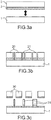
- FIG. 3a Another embodiment of the invention is illustrated on the figures 3a-3b .
- direct bonding of the substrate to be handled 1 is carried out with the handle substrate 2 covered with the bonding layer 3 of porous material.
- the figure 3b one proceeds after direct bonding to a step of cutting the handle substrate 2 to form trenches therefrom isolating regions 20, of the handle substrate from each other. Regions of variable width (5, 10, 20 and 40mm) have thus been isolated. Sealed areas will be created at the edge of each region. So in reference to the figure 3c , annealing at 900 ° C.
- a trench for example annular
- one or more trenches can be made in the substrate to be handled 1. It is then possible to induce a separation of this substrate 1 directly in the form of chips.
Landscapes
- Chemical & Material Sciences (AREA)
- Organic Chemistry (AREA)
- Element Separation (AREA)
- Container, Conveyance, Adherence, Positioning, Of Wafer (AREA)
Claims (13)
- Verfahren zum Herstellen einer Haltleiterstruktur, umfassend die Schritte:- direktes Bonden eines zu handhabenden Substrats (1, 10) mit einem Griffsubstrat (2) über eine das Griffsubstrat bedeckende Haftschicht (3), um eine Übergangsstruktur (6, 16) zu bilden, die technologischen Schritten unterworfen werden kann; und- Abbau der Übergangsstruktur im Bereich der Haftschicht, um das zu handhabende Substrat (1, 10) vom Griffsubstrat (2) zu trennen,wobei das Verfahren einen vorherigen Schritt des Abscheidens der Haftschicht (3) auf das Griffsubstrat (2) und/oder auf das zu handhabende Substrat (1) umfasst, wobei die Haftschicht eine poröse Schicht aus Organosiliziummaterial SiOC(H) ist, und
wobei der Schritt des Abbaus durch Einbringen eines Abbauwärmeeintrags in die Zwischenstruktur (6, 16) erfolgt, wobei das Einbringen zu einem spontanen Abbau der Übergangsstruktur im Bereich der Haftschicht führt. - Verfahren nach Anspruch 1, wobei das Einbringen des Abbauwärmeeintrags unter kontrollierter Atmosphäre, beispielsweise unter Stickstoffatmosphäre oder unter N2-O2-Mischatmosphäre erfolgt.
- Verfahren nach einem der Ansprüche 1 und 2, wobei das Einbringen des Abbauwärmeeintrags ein Tempern ist, das bei einer Temperatur von über 600°C über einen Zeitraum von über 10 Minuten erfolgt.
- Verfahren nach einem der Ansprüche 1 bis 3, ferner umfassend einen Schritt des Verstärkens des Bondens, der durch Einbringen eines Verstärkungswärmeeintrags in die Übergangsstruktur (6, 16) erfolgt.
- Verfahren nach einem der Ansprüche 1 bis 4, ferner umfassend vor dem Schritt des Abbaus einen Schritt des Zusammenfügens einer freien Rückseite des zu handhabenden Substrats mit einem Empfängersubstrat (11).
- Verfahren nach einem der Ansprüche 1 bis 5, ferner umfassend einen Schritt des Wiederverwertens des Griffsubstrats, umfassend das Entfernen von Rückständen (3') von der Haftschicht, die nach dem Schritt des Abbaus an der Oberfläche des Griffsubstrats (2) vorhanden sind, durch selektives Ätzen.
- Verfahren nach einem der Ansprüche 1 bis 6, wobei die Haftschicht einen Porositätsgrad zwischen 10% und 80%, vorzugsweise zwischen 15 % und 35 %, aufweist.
- Verfahren nach einem der Ansprüche 1 bis 7, wobei die Abscheidung der Haftschicht die Abscheidung eines Matrixvorläufers auf das Griffsubstrat und das Einbringen eines Porenbildners in die Abscheidung des Matrixvorläufers umfasst.
- Verfahren nach einem der Ansprüche 1 bis 8, umfassend nach der Abscheidung der Haftschicht einen Schritt der Modifizierung der Porosität der Haftschicht durch thermische, chemische, UV-, Elektronenstrahl- oder Plasmanachbehandlung.
- Verfahren nach einem der Ansprüche 1 bis 9, umfassend nach dem Schritt des direkten Bondens das Bilden von zumindest einem Graben in dem Griffsubstrat, um Bereiche (20, 21) des Griffsubstrats voneinander zu isolieren, wobei der Abbau der Übergangsstruktur zu einer teilweisen Trennung des Griffsubstrats an mindestens einem isolierten Bereich (20) des Griffsubstrats führt.
- Verfahren nach Anspruch 10, umfassend das Bilden eines Grabens in dem Griffsubstrat, um einen Kernteil des Griffsubstrats von einem Umfangsteil des Griffsubstrats zu trennen, wobei der Abbau der Übergangsstruktur zu einer teilweisen Trennung des Griffsubstrats im Bereich des Kernteils des Griffsubstrats führt, wobei das zu handhabende Substrat auf dem Umfangsteil des Griffsubstrats aufliegt.
- Verfahren nach Anspruch 11, umfassend ein Verjüngen des zu handhabenden Substrats, das auf dem Umfangsteil des Griffsubstrats aufliegt.
- Verfahren nach einem der Ansprüche 1 bis 12, umfassend nach dem Schritt des direkten Bondens das Bilden von einem oder mehreren Gräben in dem zu handhabenden Substrat, um Bereiche des zu handhabenden Substrats voneinander zu isolieren, wobei der Abbau der Übergangsstruktur zu einer teilweisen Trennung des zu handhabenden Substrats an einem oder mehreren isolierten Bereichen des zu handhabenden Substrats führt.
Applications Claiming Priority (2)
| Application Number | Priority Date | Filing Date | Title |
|---|---|---|---|
| FR1557689A FR3040108B1 (fr) | 2015-08-12 | 2015-08-12 | Procede de fabrication d'une structure semi-conductrice avec collage direct temporaire exploitant une couche poreuse |
| PCT/EP2016/068845 WO2017025494A1 (fr) | 2015-08-12 | 2016-08-08 | Procédé de fabrication d'une structure semi-conductrice avec collage direct temporaire exploitant une couche poreuse |
Publications (2)
| Publication Number | Publication Date |
|---|---|
| EP3335239A1 EP3335239A1 (de) | 2018-06-20 |
| EP3335239B1 true EP3335239B1 (de) | 2020-02-12 |
Family
ID=54291500
Family Applications (1)
| Application Number | Title | Priority Date | Filing Date |
|---|---|---|---|
| EP16750789.6A Active EP3335239B1 (de) | 2015-08-12 | 2016-08-08 | Verfahren zum herstellen einer halbleiterstruktur mit temporärem direktbonden anhand einer porösen schicht |
Country Status (4)
| Country | Link |
|---|---|
| US (1) | US10643884B2 (de) |
| EP (1) | EP3335239B1 (de) |
| FR (1) | FR3040108B1 (de) |
| WO (1) | WO2017025494A1 (de) |
Families Citing this family (5)
| Publication number | Priority date | Publication date | Assignee | Title |
|---|---|---|---|---|
| FR3085957B1 (fr) | 2018-09-14 | 2021-01-29 | Commissariat Energie Atomique | Procede de collage temporaire avec adhesif thermoplastique incorporant une couronne rigide |
| FR3088480B1 (fr) | 2018-11-09 | 2020-12-04 | Commissariat Energie Atomique | Procede de collage avec desorption stimulee electroniquement |
| FR3098342B1 (fr) * | 2019-07-02 | 2021-06-04 | Soitec Silicon On Insulator | structure semi-conductrice comprenant une couche poreuse enterrée, pour applications RF |
| WO2021229734A1 (ja) * | 2020-05-14 | 2021-11-18 | 三菱電機株式会社 | 半導体装置および半導体装置の製造方法 |
| JP2023550606A (ja) | 2020-11-03 | 2023-12-04 | コーニング インコーポレイテッド | 仮結合プロセスを使用する基板の薄化 |
Family Cites Families (19)
| Publication number | Priority date | Publication date | Assignee | Title |
|---|---|---|---|---|
| US6417069B1 (en) * | 1999-03-25 | 2002-07-09 | Canon Kabushiki Kaisha | Substrate processing method and manufacturing method, and anodizing apparatus |
| JP4538785B2 (ja) * | 2004-03-31 | 2010-09-08 | 和樹 中西 | 有機無機ハイブリッド系多孔質体の製造方法 |
| FR2876220B1 (fr) | 2004-10-06 | 2007-09-28 | Commissariat Energie Atomique | Procede d'elaboration de structures empilees mixtes, a zones isolantes diverses et/ou zones de conduction electrique verticale localisees. |
| US7462552B2 (en) * | 2005-05-23 | 2008-12-09 | Ziptronix, Inc. | Method of detachable direct bonding at low temperatures |
| FR2895419B1 (fr) | 2005-12-27 | 2008-02-22 | Commissariat Energie Atomique | Procede de realisation simplifiee d'une structure epitaxiee |
| FR2895571B1 (fr) * | 2005-12-28 | 2008-04-18 | Commissariat Energie Atomique | Procede de realisation d'une jonction pn electroluminescente en materiau semi-conducteur par collage moleculaire |
| FR2899594A1 (fr) | 2006-04-10 | 2007-10-12 | Commissariat Energie Atomique | Procede d'assemblage de substrats avec traitements thermiques a basses temperatures |
| FR2917235B1 (fr) | 2007-06-06 | 2010-09-03 | Soitec Silicon On Insulator | Procede de realisation de composants hybrides. |
| FR2929447B1 (fr) | 2008-03-28 | 2010-05-28 | Commissariat Energie Atomique | Procede de realisation d'une couche contrainte |
| US8736014B2 (en) * | 2008-11-14 | 2014-05-27 | Taiwan Semiconductor Manufacturing Company, Ltd. | High mechanical strength additives for porous ultra low-k material |
| FR2960340B1 (fr) | 2010-05-21 | 2012-06-29 | Commissariat Energie Atomique | Procede de realisation d'un support de substrat |
| KR20120080926A (ko) * | 2011-01-10 | 2012-07-18 | 삼성전자주식회사 | 다공성 저유전막을 포함하는 반도체 소자의 제조방법 |
| FR2971885A1 (fr) * | 2011-02-18 | 2012-08-24 | Commissariat Energie Atomique | Procédé de réalisation d'un support de substrat |
| FR2977884B1 (fr) | 2011-07-12 | 2016-01-29 | Commissariat Energie Atomique | Procede de realisation d'une structure a membrane suspendue et a electrode enterree |
| FR2977885A1 (fr) | 2011-07-12 | 2013-01-18 | Commissariat Energie Atomique | Procede de realisation d'une structure a electrode enterree par report direct et structure ainsi obtenue |
| FR2982414B1 (fr) | 2011-11-09 | 2014-08-22 | Commissariat Energie Atomique | Procede ameliore de realisation d'un dispositif a cavite formee entre un element suspendu reposant sur des plots isolants semi-enterres dans un substrat et ce substrat |
| FR2987626B1 (fr) * | 2012-03-05 | 2015-04-03 | Commissariat Energie Atomique | Procede de collage direct utilisant une couche poreuse compressible |
| FR3002812B1 (fr) * | 2013-03-01 | 2016-08-05 | St Microelectronics Crolles 2 Sas | Procede de transfert de couche |
| CA2907589C (en) | 2013-03-18 | 2017-11-21 | Asahi Kasei Medical Co., Ltd. | Aggregate-removing filter material, aggregate removal method, white blood cell-removing filter, and blood product filtering method |
-
2015
- 2015-08-12 FR FR1557689A patent/FR3040108B1/fr not_active Expired - Fee Related
-
2016
- 2016-08-08 EP EP16750789.6A patent/EP3335239B1/de active Active
- 2016-08-08 US US15/751,043 patent/US10643884B2/en active Active
- 2016-08-08 WO PCT/EP2016/068845 patent/WO2017025494A1/fr not_active Ceased
Non-Patent Citations (1)
| Title |
|---|
| None * |
Also Published As
| Publication number | Publication date |
|---|---|
| EP3335239A1 (de) | 2018-06-20 |
| US20180358261A1 (en) | 2018-12-13 |
| FR3040108A1 (fr) | 2017-02-17 |
| FR3040108B1 (fr) | 2017-08-11 |
| WO2017025494A1 (fr) | 2017-02-16 |
| US10643884B2 (en) | 2020-05-05 |
Similar Documents
| Publication | Publication Date | Title |
|---|---|---|
| EP2073260B1 (de) | Übertragungsverfahren einer Dünnschicht | |
| EP2004768B1 (de) | Verfahren zum assemblieren von substraten mit wärmebehandlungen bei niedrigen temperaturen | |
| EP1902463B1 (de) | Verfahren zur verringerung der rauhigkeit einer dicken isolationsschicht | |
| EP3335239B1 (de) | Verfahren zum herstellen einer halbleiterstruktur mit temporärem direktbonden anhand einer porösen schicht | |
| WO2001093325A1 (fr) | Substrat fragilise et procede de fabrication d'un tel substrat | |
| EP4128329B1 (de) | Verfahren zur herstellung einer verbundstruktur mit einer dünnen schicht aus monokristallinem sic auf einem trägersubstrat aus sic | |
| FR2938975A1 (fr) | Procede de realisation d'une heterostructure de type silicium sur saphir | |
| EP4128328B1 (de) | Verfahren zur herstellung einer verbundstruktur mit einer dünnen schicht aus monokristallinem sic auf einem trägersubstrat aus sic | |
| WO2009087290A1 (fr) | Procédé de fabrication d'une structure micro-électronique impliquant un collage moléculaire | |
| EP3818561B1 (de) | Substrat für eine integrierte hochfrequenzvorrichtung und verfahren zur herstellung davon | |
| FR2995136A1 (fr) | Pseudo-substrat avec efficacite amelioree d'utilisation d'un materiau monocristallin | |
| EP4406004A1 (de) | Verfahren zur herstellung eines polykristallinen siliciumcarbidträgersubstrats | |
| WO2021191527A1 (fr) | Procede de fabrication d'une structure empilee | |
| FR3120737A1 (fr) | Procede de fabrication d’une structure semi-conductrice a base de carbure de silicium et structure composite intermediaire | |
| FR3120736A1 (fr) | Procede de fabrication d’une structure semi-conductrice a base de carbure de silicium et structure composite intermediaire | |
| FR2918792A1 (fr) | Procede de traitement de defauts d'interface dans un substrat. | |
| FR2933235A1 (fr) | Substrat bon marche et procede de fabrication associe | |
| FR2928031A1 (fr) | Procede de transfert d'une couche mince sur un substrat support. | |
| EP2979296A1 (de) | Verfahren zur herstellung einer verbundstruktur | |
| EP1644969B1 (de) | Verfahren zur implantation durch eine irreguläre oberfläche | |
| FR2915624A1 (fr) | Procedes de collage et de fabrication d'un substrat du type a couche enterree tres fine. | |
| FR2873235A1 (fr) | Procede d'obtention d'un substrat demontable a energie de collage controlee | |
| EP1861873A1 (de) | Verfahren zur herstellung einer heterostruktur mit mindestens einer dicken schicht aus halbleitermaterial | |
| WO2026061720A1 (fr) | Procédé de fabrication d'une structure semi-conductrice à base de carbure de silicium et structure composite intermédiaire | |
| WO2023057700A1 (fr) | Procede de fabrication d'une structure composite comprenant une couche mince en sic monocristallin sur un substrat support en sic poly-cristallin |
Legal Events
| Date | Code | Title | Description |
|---|---|---|---|
| STAA | Information on the status of an ep patent application or granted ep patent |
Free format text: STATUS: THE INTERNATIONAL PUBLICATION HAS BEEN MADE |
|
| PUAI | Public reference made under article 153(3) epc to a published international application that has entered the european phase |
Free format text: ORIGINAL CODE: 0009012 |
|
| STAA | Information on the status of an ep patent application or granted ep patent |
Free format text: STATUS: REQUEST FOR EXAMINATION WAS MADE |
|
| 17P | Request for examination filed |
Effective date: 20180213 |
|
| AK | Designated contracting states |
Kind code of ref document: A1 Designated state(s): AL AT BE BG CH CY CZ DE DK EE ES FI FR GB GR HR HU IE IS IT LI LT LU LV MC MK MT NL NO PL PT RO RS SE SI SK SM TR |
|
| AX | Request for extension of the european patent |
Extension state: BA ME |
|
| DAV | Request for validation of the european patent (deleted) | ||
| DAX | Request for extension of the european patent (deleted) | ||
| STAA | Information on the status of an ep patent application or granted ep patent |
Free format text: STATUS: EXAMINATION IS IN PROGRESS |
|
| 17Q | First examination report despatched |
Effective date: 20190402 |
|
| GRAP | Despatch of communication of intention to grant a patent |
Free format text: ORIGINAL CODE: EPIDOSNIGR1 |
|
| STAA | Information on the status of an ep patent application or granted ep patent |
Free format text: STATUS: GRANT OF PATENT IS INTENDED |
|
| INTG | Intention to grant announced |
Effective date: 20190821 |
|
| GRAJ | Information related to disapproval of communication of intention to grant by the applicant or resumption of examination proceedings by the epo deleted |
Free format text: ORIGINAL CODE: EPIDOSDIGR1 |
|
| STAA | Information on the status of an ep patent application or granted ep patent |
Free format text: STATUS: EXAMINATION IS IN PROGRESS |
|
| GRAR | Information related to intention to grant a patent recorded |
Free format text: ORIGINAL CODE: EPIDOSNIGR71 |
|
| GRAS | Grant fee paid |
Free format text: ORIGINAL CODE: EPIDOSNIGR3 |
|
| STAA | Information on the status of an ep patent application or granted ep patent |
Free format text: STATUS: GRANT OF PATENT IS INTENDED |
|
| INTC | Intention to grant announced (deleted) | ||
| GRAA | (expected) grant |
Free format text: ORIGINAL CODE: 0009210 |
|
| STAA | Information on the status of an ep patent application or granted ep patent |
Free format text: STATUS: THE PATENT HAS BEEN GRANTED |
|
| INTG | Intention to grant announced |
Effective date: 20191220 |
|
| AK | Designated contracting states |
Kind code of ref document: B1 Designated state(s): AL AT BE BG CH CY CZ DE DK EE ES FI FR GB GR HR HU IE IS IT LI LT LU LV MC MK MT NL NO PL PT RO RS SE SI SK SM TR |
|
| REG | Reference to a national code |
Ref country code: GB Ref legal event code: FG4D Free format text: NOT ENGLISH |
|
| REG | Reference to a national code |
Ref country code: CH Ref legal event code: EP |
|
| REG | Reference to a national code |
Ref country code: AT Ref legal event code: REF Ref document number: 1233224 Country of ref document: AT Kind code of ref document: T Effective date: 20200215 |
|
| REG | Reference to a national code |
Ref country code: IE Ref legal event code: FG4D Free format text: LANGUAGE OF EP DOCUMENT: FRENCH |
|
| REG | Reference to a national code |
Ref country code: DE Ref legal event code: R096 Ref document number: 602016029576 Country of ref document: DE |
|
| PG25 | Lapsed in a contracting state [announced via postgrant information from national office to epo] |
Ref country code: FI Free format text: LAPSE BECAUSE OF FAILURE TO SUBMIT A TRANSLATION OF THE DESCRIPTION OR TO PAY THE FEE WITHIN THE PRESCRIBED TIME-LIMIT Effective date: 20200212 Ref country code: NO Free format text: LAPSE BECAUSE OF FAILURE TO SUBMIT A TRANSLATION OF THE DESCRIPTION OR TO PAY THE FEE WITHIN THE PRESCRIBED TIME-LIMIT Effective date: 20200512 Ref country code: RS Free format text: LAPSE BECAUSE OF FAILURE TO SUBMIT A TRANSLATION OF THE DESCRIPTION OR TO PAY THE FEE WITHIN THE PRESCRIBED TIME-LIMIT Effective date: 20200212 |
|
| REG | Reference to a national code |
Ref country code: LT Ref legal event code: MG4D |
|
| REG | Reference to a national code |
Ref country code: NL Ref legal event code: MP Effective date: 20200212 |
|
| PG25 | Lapsed in a contracting state [announced via postgrant information from national office to epo] |
Ref country code: GR Free format text: LAPSE BECAUSE OF FAILURE TO SUBMIT A TRANSLATION OF THE DESCRIPTION OR TO PAY THE FEE WITHIN THE PRESCRIBED TIME-LIMIT Effective date: 20200513 Ref country code: HR Free format text: LAPSE BECAUSE OF FAILURE TO SUBMIT A TRANSLATION OF THE DESCRIPTION OR TO PAY THE FEE WITHIN THE PRESCRIBED TIME-LIMIT Effective date: 20200212 Ref country code: LV Free format text: LAPSE BECAUSE OF FAILURE TO SUBMIT A TRANSLATION OF THE DESCRIPTION OR TO PAY THE FEE WITHIN THE PRESCRIBED TIME-LIMIT Effective date: 20200212 Ref country code: SE Free format text: LAPSE BECAUSE OF FAILURE TO SUBMIT A TRANSLATION OF THE DESCRIPTION OR TO PAY THE FEE WITHIN THE PRESCRIBED TIME-LIMIT Effective date: 20200212 Ref country code: IS Free format text: LAPSE BECAUSE OF FAILURE TO SUBMIT A TRANSLATION OF THE DESCRIPTION OR TO PAY THE FEE WITHIN THE PRESCRIBED TIME-LIMIT Effective date: 20200612 Ref country code: BG Free format text: LAPSE BECAUSE OF FAILURE TO SUBMIT A TRANSLATION OF THE DESCRIPTION OR TO PAY THE FEE WITHIN THE PRESCRIBED TIME-LIMIT Effective date: 20200512 |
|
| PG25 | Lapsed in a contracting state [announced via postgrant information from national office to epo] |
Ref country code: NL Free format text: LAPSE BECAUSE OF FAILURE TO SUBMIT A TRANSLATION OF THE DESCRIPTION OR TO PAY THE FEE WITHIN THE PRESCRIBED TIME-LIMIT Effective date: 20200212 |
|
| PG25 | Lapsed in a contracting state [announced via postgrant information from national office to epo] |
Ref country code: RO Free format text: LAPSE BECAUSE OF FAILURE TO SUBMIT A TRANSLATION OF THE DESCRIPTION OR TO PAY THE FEE WITHIN THE PRESCRIBED TIME-LIMIT Effective date: 20200212 Ref country code: CZ Free format text: LAPSE BECAUSE OF FAILURE TO SUBMIT A TRANSLATION OF THE DESCRIPTION OR TO PAY THE FEE WITHIN THE PRESCRIBED TIME-LIMIT Effective date: 20200212 Ref country code: SM Free format text: LAPSE BECAUSE OF FAILURE TO SUBMIT A TRANSLATION OF THE DESCRIPTION OR TO PAY THE FEE WITHIN THE PRESCRIBED TIME-LIMIT Effective date: 20200212 Ref country code: EE Free format text: LAPSE BECAUSE OF FAILURE TO SUBMIT A TRANSLATION OF THE DESCRIPTION OR TO PAY THE FEE WITHIN THE PRESCRIBED TIME-LIMIT Effective date: 20200212 Ref country code: LT Free format text: LAPSE BECAUSE OF FAILURE TO SUBMIT A TRANSLATION OF THE DESCRIPTION OR TO PAY THE FEE WITHIN THE PRESCRIBED TIME-LIMIT Effective date: 20200212 Ref country code: DK Free format text: LAPSE BECAUSE OF FAILURE TO SUBMIT A TRANSLATION OF THE DESCRIPTION OR TO PAY THE FEE WITHIN THE PRESCRIBED TIME-LIMIT Effective date: 20200212 Ref country code: ES Free format text: LAPSE BECAUSE OF FAILURE TO SUBMIT A TRANSLATION OF THE DESCRIPTION OR TO PAY THE FEE WITHIN THE PRESCRIBED TIME-LIMIT Effective date: 20200212 Ref country code: PT Free format text: LAPSE BECAUSE OF FAILURE TO SUBMIT A TRANSLATION OF THE DESCRIPTION OR TO PAY THE FEE WITHIN THE PRESCRIBED TIME-LIMIT Effective date: 20200705 Ref country code: SK Free format text: LAPSE BECAUSE OF FAILURE TO SUBMIT A TRANSLATION OF THE DESCRIPTION OR TO PAY THE FEE WITHIN THE PRESCRIBED TIME-LIMIT Effective date: 20200212 |
|
| REG | Reference to a national code |
Ref country code: DE Ref legal event code: R097 Ref document number: 602016029576 Country of ref document: DE |
|
| REG | Reference to a national code |
Ref country code: AT Ref legal event code: MK05 Ref document number: 1233224 Country of ref document: AT Kind code of ref document: T Effective date: 20200212 |
|
| PLBE | No opposition filed within time limit |
Free format text: ORIGINAL CODE: 0009261 |
|
| STAA | Information on the status of an ep patent application or granted ep patent |
Free format text: STATUS: NO OPPOSITION FILED WITHIN TIME LIMIT |
|
| 26N | No opposition filed |
Effective date: 20201113 |
|
| PG25 | Lapsed in a contracting state [announced via postgrant information from national office to epo] |
Ref country code: IT Free format text: LAPSE BECAUSE OF FAILURE TO SUBMIT A TRANSLATION OF THE DESCRIPTION OR TO PAY THE FEE WITHIN THE PRESCRIBED TIME-LIMIT Effective date: 20200212 Ref country code: AT Free format text: LAPSE BECAUSE OF FAILURE TO SUBMIT A TRANSLATION OF THE DESCRIPTION OR TO PAY THE FEE WITHIN THE PRESCRIBED TIME-LIMIT Effective date: 20200212 |
|
| PG25 | Lapsed in a contracting state [announced via postgrant information from national office to epo] |
Ref country code: PL Free format text: LAPSE BECAUSE OF FAILURE TO SUBMIT A TRANSLATION OF THE DESCRIPTION OR TO PAY THE FEE WITHIN THE PRESCRIBED TIME-LIMIT Effective date: 20200212 Ref country code: SI Free format text: LAPSE BECAUSE OF FAILURE TO SUBMIT A TRANSLATION OF THE DESCRIPTION OR TO PAY THE FEE WITHIN THE PRESCRIBED TIME-LIMIT Effective date: 20200212 |
|
| PG25 | Lapsed in a contracting state [announced via postgrant information from national office to epo] |
Ref country code: MC Free format text: LAPSE BECAUSE OF FAILURE TO SUBMIT A TRANSLATION OF THE DESCRIPTION OR TO PAY THE FEE WITHIN THE PRESCRIBED TIME-LIMIT Effective date: 20200212 |
|
| REG | Reference to a national code |
Ref country code: CH Ref legal event code: PL |
|
| PG25 | Lapsed in a contracting state [announced via postgrant information from national office to epo] |
Ref country code: CH Free format text: LAPSE BECAUSE OF NON-PAYMENT OF DUE FEES Effective date: 20200831 Ref country code: LU Free format text: LAPSE BECAUSE OF NON-PAYMENT OF DUE FEES Effective date: 20200808 Ref country code: LI Free format text: LAPSE BECAUSE OF NON-PAYMENT OF DUE FEES Effective date: 20200831 |
|
| REG | Reference to a national code |
Ref country code: BE Ref legal event code: MM Effective date: 20200831 |
|
| PG25 | Lapsed in a contracting state [announced via postgrant information from national office to epo] |
Ref country code: IE Free format text: LAPSE BECAUSE OF NON-PAYMENT OF DUE FEES Effective date: 20200808 Ref country code: BE Free format text: LAPSE BECAUSE OF NON-PAYMENT OF DUE FEES Effective date: 20200831 |
|
| PG25 | Lapsed in a contracting state [announced via postgrant information from national office to epo] |
Ref country code: TR Free format text: LAPSE BECAUSE OF FAILURE TO SUBMIT A TRANSLATION OF THE DESCRIPTION OR TO PAY THE FEE WITHIN THE PRESCRIBED TIME-LIMIT Effective date: 20200212 Ref country code: MT Free format text: LAPSE BECAUSE OF FAILURE TO SUBMIT A TRANSLATION OF THE DESCRIPTION OR TO PAY THE FEE WITHIN THE PRESCRIBED TIME-LIMIT Effective date: 20200212 Ref country code: CY Free format text: LAPSE BECAUSE OF FAILURE TO SUBMIT A TRANSLATION OF THE DESCRIPTION OR TO PAY THE FEE WITHIN THE PRESCRIBED TIME-LIMIT Effective date: 20200212 |
|
| PG25 | Lapsed in a contracting state [announced via postgrant information from national office to epo] |
Ref country code: MK Free format text: LAPSE BECAUSE OF FAILURE TO SUBMIT A TRANSLATION OF THE DESCRIPTION OR TO PAY THE FEE WITHIN THE PRESCRIBED TIME-LIMIT Effective date: 20200212 Ref country code: AL Free format text: LAPSE BECAUSE OF FAILURE TO SUBMIT A TRANSLATION OF THE DESCRIPTION OR TO PAY THE FEE WITHIN THE PRESCRIBED TIME-LIMIT Effective date: 20200212 |
|
| PGFP | Annual fee paid to national office [announced via postgrant information from national office to epo] |
Ref country code: DE Payment date: 20250819 Year of fee payment: 10 |
|
| PGFP | Annual fee paid to national office [announced via postgrant information from national office to epo] |
Ref country code: GB Payment date: 20250825 Year of fee payment: 10 |
|
| PGFP | Annual fee paid to national office [announced via postgrant information from national office to epo] |
Ref country code: FR Payment date: 20250827 Year of fee payment: 10 |
|
| REG | Reference to a national code |
Ref country code: DE Ref legal event code: R079 Ref document number: 602016029576 Country of ref document: DE Free format text: PREVIOUS MAIN CLASS: H01L0021762000 Ipc: H10W0010100000 |