EP3338302B1 - Carte de circuits imprimés et ensemble électronique de puissance équipé d'une carte de circuits imprimés - Google Patents
Carte de circuits imprimés et ensemble électronique de puissance équipé d'une carte de circuits imprimés Download PDFInfo
- Publication number
- EP3338302B1 EP3338302B1 EP16750791.2A EP16750791A EP3338302B1 EP 3338302 B1 EP3338302 B1 EP 3338302B1 EP 16750791 A EP16750791 A EP 16750791A EP 3338302 B1 EP3338302 B1 EP 3338302B1
- Authority
- EP
- European Patent Office
- Prior art keywords
- copper
- circuit carrier
- layer
- copper layer
- heat sink
- Prior art date
- Legal status (The legal status is an assumption and is not a legal conclusion. Google has not performed a legal analysis and makes no representation as to the accuracy of the status listed.)
- Active
Links
Images
Classifications
-
- H—ELECTRICITY
- H10—SEMICONDUCTOR DEVICES; ELECTRIC SOLID-STATE DEVICES NOT OTHERWISE PROVIDED FOR
- H10W—GENERIC PACKAGES, INTERCONNECTIONS, CONNECTORS OR OTHER CONSTRUCTIONAL DETAILS OF DEVICES COVERED BY CLASS H10
- H10W40/00—Arrangements for thermal protection or thermal control
- H10W40/20—Arrangements for cooling
- H10W40/25—Arrangements for cooling characterised by their materials
- H10W40/255—Arrangements for cooling characterised by their materials having a laminate or multilayered structure, e.g. direct bond copper [DBC] ceramic substrates
-
- C—CHEMISTRY; METALLURGY
- C23—COATING METALLIC MATERIAL; COATING MATERIAL WITH METALLIC MATERIAL; CHEMICAL SURFACE TREATMENT; DIFFUSION TREATMENT OF METALLIC MATERIAL; COATING BY VACUUM EVAPORATION, BY SPUTTERING, BY ION IMPLANTATION OR BY CHEMICAL VAPOUR DEPOSITION, IN GENERAL; INHIBITING CORROSION OF METALLIC MATERIAL OR INCRUSTATION IN GENERAL
- C23C—COATING METALLIC MATERIAL; COATING MATERIAL WITH METALLIC MATERIAL; SURFACE TREATMENT OF METALLIC MATERIAL BY DIFFUSION INTO THE SURFACE, BY CHEMICAL CONVERSION OR SUBSTITUTION; COATING BY VACUUM EVAPORATION, BY SPUTTERING, BY ION IMPLANTATION OR BY CHEMICAL VAPOUR DEPOSITION, IN GENERAL
- C23C24/00—Coating starting from inorganic powder
- C23C24/02—Coating starting from inorganic powder by application of pressure only
- C23C24/04—Impact or kinetic deposition of particles
-
- C—CHEMISTRY; METALLURGY
- C23—COATING METALLIC MATERIAL; COATING MATERIAL WITH METALLIC MATERIAL; CHEMICAL SURFACE TREATMENT; DIFFUSION TREATMENT OF METALLIC MATERIAL; COATING BY VACUUM EVAPORATION, BY SPUTTERING, BY ION IMPLANTATION OR BY CHEMICAL VAPOUR DEPOSITION, IN GENERAL; INHIBITING CORROSION OF METALLIC MATERIAL OR INCRUSTATION IN GENERAL
- C23C—COATING METALLIC MATERIAL; COATING MATERIAL WITH METALLIC MATERIAL; SURFACE TREATMENT OF METALLIC MATERIAL BY DIFFUSION INTO THE SURFACE, BY CHEMICAL CONVERSION OR SUBSTITUTION; COATING BY VACUUM EVAPORATION, BY SPUTTERING, BY ION IMPLANTATION OR BY CHEMICAL VAPOUR DEPOSITION, IN GENERAL
- C23C28/00—Coating for obtaining at least two superposed coatings either by methods not provided for in a single one of groups C23C2/00 - C23C26/00 or by combinations of methods provided for in subclasses C23C and C25C or C25D
- C23C28/30—Coatings combining at least one metallic layer and at least one inorganic non-metallic layer
- C23C28/32—Coatings combining at least one metallic layer and at least one inorganic non-metallic layer including at least one pure metallic layer
- C23C28/321—Coatings combining at least one metallic layer and at least one inorganic non-metallic layer including at least one pure metallic layer with at least one metal alloy layer
-
- H—ELECTRICITY
- H10—SEMICONDUCTOR DEVICES; ELECTRIC SOLID-STATE DEVICES NOT OTHERWISE PROVIDED FOR
- H10W—GENERIC PACKAGES, INTERCONNECTIONS, CONNECTORS OR OTHER CONSTRUCTIONAL DETAILS OF DEVICES COVERED BY CLASS H10
- H10W70/00—Package substrates; Interposers; Redistribution layers [RDL]
- H10W70/20—Conductive package substrates serving as an interconnection, e.g. metal plates
-
- H—ELECTRICITY
- H10—SEMICONDUCTOR DEVICES; ELECTRIC SOLID-STATE DEVICES NOT OTHERWISE PROVIDED FOR
- H10W—GENERIC PACKAGES, INTERCONNECTIONS, CONNECTORS OR OTHER CONSTRUCTIONAL DETAILS OF DEVICES COVERED BY CLASS H10
- H10W70/00—Package substrates; Interposers; Redistribution layers [RDL]
- H10W70/40—Leadframes
- H10W70/461—Leadframes specially adapted for cooling
-
- H—ELECTRICITY
- H10—SEMICONDUCTOR DEVICES; ELECTRIC SOLID-STATE DEVICES NOT OTHERWISE PROVIDED FOR
- H10W—GENERIC PACKAGES, INTERCONNECTIONS, CONNECTORS OR OTHER CONSTRUCTIONAL DETAILS OF DEVICES COVERED BY CLASS H10
- H10W72/00—Interconnections or connectors in packages
- H10W72/071—Connecting or disconnecting
- H10W72/073—Connecting or disconnecting of die-attach connectors
- H10W72/07331—Connecting techniques
- H10W72/07336—Soldering or alloying
-
- H—ELECTRICITY
- H10—SEMICONDUCTOR DEVICES; ELECTRIC SOLID-STATE DEVICES NOT OTHERWISE PROVIDED FOR
- H10W—GENERIC PACKAGES, INTERCONNECTIONS, CONNECTORS OR OTHER CONSTRUCTIONAL DETAILS OF DEVICES COVERED BY CLASS H10
- H10W72/00—Interconnections or connectors in packages
- H10W72/50—Bond wires
- H10W72/531—Shapes of wire connectors
- H10W72/5363—Shapes of wire connectors the connected ends being wedge-shaped
-
- H—ELECTRICITY
- H10—SEMICONDUCTOR DEVICES; ELECTRIC SOLID-STATE DEVICES NOT OTHERWISE PROVIDED FOR
- H10W—GENERIC PACKAGES, INTERCONNECTIONS, CONNECTORS OR OTHER CONSTRUCTIONAL DETAILS OF DEVICES COVERED BY CLASS H10
- H10W72/00—Interconnections or connectors in packages
- H10W72/851—Dispositions of multiple connectors or interconnections
- H10W72/874—On different surfaces
- H10W72/884—Die-attach connectors and bond wires
-
- H—ELECTRICITY
- H10—SEMICONDUCTOR DEVICES; ELECTRIC SOLID-STATE DEVICES NOT OTHERWISE PROVIDED FOR
- H10W—GENERIC PACKAGES, INTERCONNECTIONS, CONNECTORS OR OTHER CONSTRUCTIONAL DETAILS OF DEVICES COVERED BY CLASS H10
- H10W90/00—Package configurations
- H10W90/701—Package configurations characterised by the relative positions of pads or connectors relative to package parts
- H10W90/731—Package configurations characterised by the relative positions of pads or connectors relative to package parts of die-attach connectors
- H10W90/734—Package configurations characterised by the relative positions of pads or connectors relative to package parts of die-attach connectors between a chip and a stacked insulating package substrate, interposer or RDL
-
- H—ELECTRICITY
- H10—SEMICONDUCTOR DEVICES; ELECTRIC SOLID-STATE DEVICES NOT OTHERWISE PROVIDED FOR
- H10W—GENERIC PACKAGES, INTERCONNECTIONS, CONNECTORS OR OTHER CONSTRUCTIONAL DETAILS OF DEVICES COVERED BY CLASS H10
- H10W90/00—Package configurations
- H10W90/701—Package configurations characterised by the relative positions of pads or connectors relative to package parts
- H10W90/751—Package configurations characterised by the relative positions of pads or connectors relative to package parts of bond wires
- H10W90/754—Package configurations characterised by the relative positions of pads or connectors relative to package parts of bond wires between a chip and a stacked insulating package substrate, interposer or RDL
Definitions
- the invention relates to a circuit carrier for holding at least one electric power component and a power electronics assembly with a said circuit carrier.
- a circuit carrier for holding electric power components which has a heat sink for holding and for cooling the power components.
- the heat sink has a surface on which a copper layer is formed.
- Power components are usually arranged on ceramic circuit carriers (DCB), which have a good thermal conductivity due to their high power losses and thus the bound heat generation.
- DCB ceramic circuit carriers
- the heat dissipation but over the ceramic circuit substrate is not sufficiently efficient, so that protection of the power devices from overheating is not sufficiently secured.
- the ceramic circuit boards are expensive.
- in some applications such. As in the automotive sector, esp. In the field of hybrid electric / electric vehicles, better heat dissipation desirable.
- the object of the present invention is to provide a way for efficient and cost-effective heat dissipation for the power devices.
- a circuit carrier for holding at least one power device.
- the circuit carrier comprises a heat sink with a surface which is designed for holding and for cooling the power component.
- the circuit carrier further comprises a copper layer, which consists of copper or a copper alloy and is designed to mechanically connect the heat sink with at least one copper plate.
- the copper layer is cold sprayed or sintered on the surface of the heat sink.
- the circuit carrier further comprises at least one copper plate, which is also made of copper or a copper alloy and is designed to connect the power device with the copper layer mechanically and electrically conductive.
- the copper plate is arranged directly on a surface remote from the heat sink surface of the copper layer and connected to the copper layer surface, mechanically and electrically conductive.
- a power device may in this case be a passive or an active electrical or electronic component, such.
- a power device may also be an electrical conductor designed to carry currents in excess of 100 amperes.
- the heat sink serves as a heat sink and absorbs the waste heat that arises during operation of the power device.
- the heat sink serves as a carrier of the power component or the conductor track to the power component and provides mechanical support for the power component or the conductor track.
- the heat sink replaces an expensive ceramic circuit carrier that would otherwise be required to hold the power device and the trace. This reduces costs for circuit carriers.
- the copper layer serves as a conductor for the transmission of electrical currents from / to the power device.
- the copper layer has a structured according to a predetermined circuit layout of the power electronics assembly course.
- the copper layer serves as an efficient heat transfer medium for passing the waste heat from the power component to the heat sink.
- the copper layer is formed on the surface of the heat sink in a cold gas spraying or sintering process.
- a “layer” means a flat (in particular flat) expanded covering of a corresponding material having a thickness of at most 1 millimeter, in particular a maximum of 0.5 millimeter, especially a maximum of 0.2 millimeter, and, for example, a maximum of 0, 1 millimeter.
- a copper layer is a surface-wide covering made of copper or a copper alloy with a layer thickness of less than 1 millimeter, which is produced by cold gas spraying or by sintering.
- the copper plate is a thin plate made of copper or a copper alloy, which is for example punched out of a thin sheet of copper or a copper alloy or cut out in any other way.
- a copper plate is esp. Not a copper layer, which in a cold gas spraying or sintering process or other similar coating method is formed or formed on said surface of the heat sink.
- the copper plate allows both a solder joint and a welded joint. As a welding partner, the copper plate can readily be welded, for example, with an electrical conductor, esp. Laser welded or welded with sonotrodes.
- a “planar (mechanical or electrical) connection” means a (mechanical or electrical) connection over an extended contact surface, which extends over substantially the entire electrical contact surface of an electrical connection of the power component to be electrically contacted and thus the largest possible heat transfer surface of the Power component over the copper plate and the copper layer to the heat sink provides.
- the "area connection” allows efficient heat dissipation from the power device to the heat sink.
- a "direct arrangement” means an arrangement of the power device on the copper plate which is formed only via a direct interconnect layer and without further interlayers or other intermediate elements that are not primarily designed for direct mechanical and physical connection of the power device to the copper plate.
- the power device is only connected via a connecting layer directly to the copper plate surface, mechanically and electrically conductive.
- the copper layer and the copper plate made of copper or a copper alloy have very high thermal conductivities and thus enable efficient heat dissipation for the power component.
- the copper layer allows a cost-effective mechanical connection of the copper plate or the power component with the heat sink. Because the copper layer is cold-gas injected or sintered on the surface of the heat sink, the copper layer has a high ductility and can compensate for different thermal expansions between the heat sink and the copper plate or the power component. Thus, the copper layer ensures that the copper plate and thus also the power device remain securely adhered to the heat sink despite the mechanical stresses due to the different thermal expansions.
- the copper layer preferably has a layer thickness which is at least 45 micrometers, in particular at least 50 micrometers, especially at least 100 micrometers.
- the copper plate is preferably soldered on the surface of the copper layer and serves as a bonding surface for bonding the copper layer to at least one power device.
- the bonding surface of the copper plate provides a stable electrical and mechanical connection for the high current terminals of the power devices.
- the copper plate preferably has a material thickness which is at least 0.9 millimeters, in particular at least 1 millimeter, especially at least 2 millimeters.
- the circuit carrier further comprises an insulating layer which is arranged between the surface of the heat sink and the copper layer and mechanically connects the copper layer with the heat sink and at the same time electrically insulated.
- the insulating layer of an electrically insulating and thermally conductive material, esp. A ceramic is formed.
- the insulating layer is cold sprayed or sintered on the surface of the heat sink.
- the insulating layer has a layer thickness sufficiently thick to effectively electrically insulate the copper layer from the (optionally electrically conductive) heat sink, and is sufficiently thin to efficiently transfer the waste heat from the power device to the heat sink.
- a power electronics assembly comprises at least one power component and at least one circuit carrier described above.
- the power component is arranged on a side facing away from the heat sink surface of the copper plate of the circuit substrate and connected to the copper plate surface, mechanically and electrically conductive.
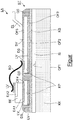
- FIGURE shows a schematic cross-sectional representation of a power electronics assembly LA according to an embodiment of the invention.
- the power electronics assembly LA shown in the figure is for example a part of an inverter or an output stage of the inverter for an electric drive of a hybrid electric / electric vehicle.
- the power electronics assembly LA comprises a circuit carrier ST and a power semiconductor switch (power component) BE mounted on the circuit carrier ST.
- the circuit carrier ST comprises a heat sink KK, which consists of aluminum and is produced in a die-casting process.
- the heat sink KK has a planar surface OF1, on which an insulating layer IS is arranged.
- the insulating layer IS consists of an electrically insulating, thermally conductive ceramic and is coated in a cold gas spraying process on the surface OF1 of the heat sink KK.
- the insulating layer IS electrically isolates the power semiconductor switch BE from the heat sink KK and at the same time transfers waste heat from the power semiconductor switch BE to the heat sink KK.
- the circuit carrier ST on a copper layer KS which consists of a copper alloy and is coated in a further cold gas spraying on the surface OF2.
- the copper layer KS serves for the mechanical and electrical Connection of copper plates KP to be described below with the heat sink KK.
- the circuit carrier ST on two copper plates KP, which are soldered to the copper layer KS areally, mechanically and electrically conductive.
- the power semiconductor switch BE On a side remote from the heat sink KK surface OF4 one of the two copper plates KP the power semiconductor switch BE is arranged.
- the power semiconductor switch BE has on a surface on a surface formed electrical connection EA1, which is soldered via a solder joint LV with the copper plate KP surface, mechanically and electrically conductive, for example.
- a bonding wire BD is arranged, which is mechanically and electrically conductively connected via a solder joint LV with the copper plate KP.
- the bonding wire BD is further mechanically and electrically soldered to a further electrical connection EA2 of the power semiconductor switch BE.
- an electrical conductor EL or its contact connection is arranged on the surface OF5 of the further copper plate KP and is connected in a planar, mechanically and electrically conductive manner to the copper plate KP via a welded joint SV (for example welded with sonotrodes).
- a sealing layer DS is further arranged, which exposed, not with respective overlying layers or circuit components cover covered areas of the copper layer KS and the two copper plates KP media density and protect against environmental influences such. As the moisture, protect.
- the sealing layer DS is formed, for example, from an electrically insulating and thermally conductive molding compound, which is cast on the surfaces OF3, OF4, OF5.
Landscapes
- Chemical & Material Sciences (AREA)
- Engineering & Computer Science (AREA)
- Chemical Kinetics & Catalysis (AREA)
- Materials Engineering (AREA)
- Mechanical Engineering (AREA)
- Metallurgy (AREA)
- Organic Chemistry (AREA)
- Inorganic Chemistry (AREA)
- Cooling Or The Like Of Semiconductors Or Solid State Devices (AREA)
- Ceramic Engineering (AREA)
Claims (7)
- Porte-circuit (ST) destiné à porter au moins un composant électrique de puissance (BE) et comportant :- un corps de refroidissement (KK) qui porte et refroidit le composant électrique de puissance (BE) qui présente une surface (OF1),- une couche de cuivre (KS), la couche de cuivre (KS) étant constituée de cuivre ou d'un alliage de cuivre,
caractérisé en ce que- le porte-circuit (ST) présente en outre au moins une plaque de cuivre (KP) qui relie mécaniquement et électriquement le composant de puissance (BE) à la couche de cuivre (KS), la plaque de cuivre (KP) étant constituée de cuivre ou d'un alliage de cuivre, étant disposée directement sur une surface (OF3), non tournée vers le corps de refroidissement (KK), de la couche de cuivre (KS) et étant reliée à plat, mécaniquement et de manière électriquement conductrice à la couche de cuivre (KS),- la couche de cuivre (KS) étant configurée avec au moins une plaque de cuivre (KP) pour assurer la liaison mécanique du corps de refroidissement (KK) avec la ou les plaques de cuivre (KP) et étant formée par pulvérisation à froid en phase gazeuse ou par frittage sur la surface (OF1) du corps de refroidissement (KK). - Porte-circuit (ST) selon la revendication 1, dans lequel la couche de cuivre (KS) a une épaisseur d'au moins 45 micromètres, en particulier d'au moins 50 micromètres et notamment d'au moins 100 micromètres.
- Porte-circuit (ST) selon les revendications 1 ou 2, dans lequel la plaque de cuivre (KP) est brasée sur la surface (OF3) de la couche de cuivre (KS) et sert à assurer la liaison électrique et mécanique de la couche de cuivre avec au moins un composant de puissance (BE).
- Porte-circuit (ST) selon l'une des revendications précédentes, dans lequel la plaque de cuivre (KP) a une épaisseur d'au moins 0,9 millimètre, en particulier d'au moins 1 millimètre et notamment d'au moins 2 millimètres.
- Porte-circuit (ST) selon l'une des revendications précédentes, comportant en outre une couche isolante (IS) disposée entre la surface (OF1) du corps de refroidissement (KK) et la couche de cuivre (KS), reliant mécaniquement le corps de refroidissement (KK) à la couche de cuivre (KS) et l'isolant électriquement de cette dernière.
- Porte-circuit (ST) selon la revendication 5, dans lequel la couche isolante (IS) formée par pulvérisation à froid en phase gazeuse ou par frittage sur la surface (OF1) du corps de refroidissement (KK).
- Circuit électronique de puissance (LA) comprenant- au moins un composant électrique de puissance (BE) et- au moins un porte-circuit (ST) selon l'une des revendications précédentes, le composant de puissance (BE) étant disposé sur une surface (OF4), non tournée vers le corps de refroidissement (KK), de la plaque de cuivre (KP) et étant relié à plat, mécaniquement et de manière électriquement conductrice à la plaque de cuivre (KP).
Applications Claiming Priority (2)
| Application Number | Priority Date | Filing Date | Title |
|---|---|---|---|
| DE102015216047.5A DE102015216047A1 (de) | 2015-08-21 | 2015-08-21 | Schaltungsträger, Leistungselektronikanordnung mit einem Schaltungsträger |
| PCT/EP2016/068859 WO2017032581A1 (fr) | 2015-08-21 | 2016-08-08 | Carte de circuits imprimés et ensemble électronique de puissance équipé d'une carte de circuits imprimés |
Publications (2)
| Publication Number | Publication Date |
|---|---|
| EP3338302A1 EP3338302A1 (fr) | 2018-06-27 |
| EP3338302B1 true EP3338302B1 (fr) | 2019-05-01 |
Family
ID=56683940
Family Applications (1)
| Application Number | Title | Priority Date | Filing Date |
|---|---|---|---|
| EP16750791.2A Active EP3338302B1 (fr) | 2015-08-21 | 2016-08-08 | Carte de circuits imprimés et ensemble électronique de puissance équipé d'une carte de circuits imprimés |
Country Status (5)
| Country | Link |
|---|---|
| US (1) | US11276623B2 (fr) |
| EP (1) | EP3338302B1 (fr) |
| CN (1) | CN107924892B (fr) |
| DE (1) | DE102015216047A1 (fr) |
| WO (1) | WO2017032581A1 (fr) |
Families Citing this family (3)
| Publication number | Priority date | Publication date | Assignee | Title |
|---|---|---|---|---|
| DE102018219574A1 (de) * | 2018-11-15 | 2020-05-20 | Continental Automotive Gmbh | Schaltungsträger, (Leistungs-)Elektronikanordnung und elektrische Antriebsvorrichtung |
| DE102020205979A1 (de) | 2020-05-12 | 2021-11-18 | Robert Bosch Gesellschaft mit beschränkter Haftung | Leistungsmodul mit einer Wärmesenke |
| EP4084058A1 (fr) * | 2021-04-27 | 2022-11-02 | Siemens Aktiengesellschaft | Module électronique pourvu de porte-circuit, de puce à semi-conducteur et de dissipateur thermique |
Family Cites Families (18)
| Publication number | Priority date | Publication date | Assignee | Title |
|---|---|---|---|---|
| JPH06283639A (ja) * | 1993-03-25 | 1994-10-07 | Sanyo Electric Co Ltd | 混成集積回路 |
| JP4586823B2 (ja) * | 2007-06-21 | 2010-11-24 | トヨタ自動車株式会社 | 成膜方法、伝熱部材、パワーモジュール、車両用インバータ、及び車両 |
| JP2009038162A (ja) * | 2007-08-01 | 2009-02-19 | Sumitomo Electric Ind Ltd | 放熱部品、その製造方法及びパワーモジュール |
| JP5565147B2 (ja) * | 2010-06-30 | 2014-08-06 | 株式会社デンソー | 半導体モジュールの製造方法 |
| JP2012222327A (ja) * | 2011-04-14 | 2012-11-12 | Aisin Aw Co Ltd | 半導体装置及びその製造方法 |
| DE102011076774A1 (de) * | 2011-05-31 | 2012-12-06 | Continental Automotive Gmbh | Baugruppe mit einem Träger und einem Kühlkörper |
| JP5627789B2 (ja) * | 2011-08-04 | 2014-11-19 | 三菱電機株式会社 | 半導体装置とその製造方法 |
| KR101222831B1 (ko) * | 2011-09-16 | 2013-01-15 | 삼성전기주식회사 | 전력 모듈 패키지 |
| JP5606421B2 (ja) * | 2011-10-27 | 2014-10-15 | 株式会社日立製作所 | 銅ナノ粒子を用いた焼結性接合材料及びその製造方法及び電子部材の接合方法 |
| EP2833404A4 (fr) * | 2012-03-28 | 2016-01-20 | Fuji Electric Co Ltd | Dispositif à semi-conducteur et procédé de fabrication de dispositif à semi-conducteur |
| JP5656907B2 (ja) * | 2012-04-11 | 2015-01-21 | 三菱電機株式会社 | パワーモジュール |
| KR20150035671A (ko) * | 2012-08-08 | 2015-04-07 | 센주긴조쿠고교 가부시키가이샤 | 고온 납프리 땜납 합금 |
| CN104603933B (zh) * | 2012-08-31 | 2018-09-18 | 三菱综合材料株式会社 | 功率模块用基板及功率模块 |
| DE102013110815B3 (de) * | 2013-09-30 | 2014-10-30 | Semikron Elektronik Gmbh & Co. Kg | Leistungshalbleitereinrichtung und Verfahren zur Herstellung einer Leistungshalbleitereinrichtung |
| WO2015159751A1 (fr) * | 2014-04-14 | 2015-10-22 | 富士電機株式会社 | Dispositif à semi-conducteur |
| DE102014214784A1 (de) * | 2014-07-28 | 2016-02-11 | Continental Automotive Gmbh | Schaltungsträger, elektronische Baugruppe, Verfahren zum Herstellen eines Schaltungsträgers |
| DE102015210587B4 (de) * | 2015-06-10 | 2020-10-29 | Infineon Technologies Ag | Halbleitermodul, halbleitermodulanordnung und verfahren zum betrieb eines halbleitermoduls |
| ITUB20153344A1 (it) * | 2015-09-02 | 2017-03-02 | St Microelectronics Srl | Modulo di potenza elettronico con migliorata dissipazione termica e relativo metodo di fabbricazione |
-
2015
- 2015-08-21 DE DE102015216047.5A patent/DE102015216047A1/de not_active Ceased
-
2016
- 2016-08-08 WO PCT/EP2016/068859 patent/WO2017032581A1/fr not_active Ceased
- 2016-08-08 CN CN201680048039.8A patent/CN107924892B/zh active Active
- 2016-08-08 EP EP16750791.2A patent/EP3338302B1/fr active Active
-
2018
- 2018-02-18 US US15/898,596 patent/US11276623B2/en active Active
Non-Patent Citations (1)
| Title |
|---|
| None * |
Also Published As
| Publication number | Publication date |
|---|---|
| EP3338302A1 (fr) | 2018-06-27 |
| CN107924892B (zh) | 2021-03-23 |
| US20180174947A1 (en) | 2018-06-21 |
| WO2017032581A1 (fr) | 2017-03-02 |
| CN107924892A (zh) | 2018-04-17 |
| DE102015216047A1 (de) | 2017-02-23 |
| US11276623B2 (en) | 2022-03-15 |
Similar Documents
| Publication | Publication Date | Title |
|---|---|---|
| EP0920055B1 (fr) | Dispositif de refroidissement pour un composant générant de la chaleur sur un circuit imprimé | |
| AT512525B1 (de) | Leiterplatte, insbesondere für ein Leistungselektronikmodul, umfassend ein elektrisch leitfähiges Substrat | |
| EP1980143B1 (fr) | Carte de circuits imprimés comportant des éléments fonctionnels supplémentaires, son procédé de production et son utilisation | |
| EP2107604B1 (fr) | Module semi-conducteur de puissance doté d'un circuit étanche hermétique et son procédé de fabrication | |
| DE102019206523A1 (de) | Leistungsmodul mit gehäusten Leistungshalbleitern zur steuerbaren elektrischen Leistungsversorgung eines Verbrauchers | |
| EP3625823B1 (fr) | Module de puissance comprenant au moins un semi-conducteur de puissance | |
| EP0805494A2 (fr) | Module multi-couche semi-conducteur de puissance à haute densité d'empaquetage | |
| DE112016005766B4 (de) | Schaltungsanordnung und elektrischer anschlusskasten | |
| EP1841299A2 (fr) | Dispositif de liaison pour composant électrique | |
| DE19509441C2 (de) | Integrierte Hybrid-Leistungsschaltungsvorrichtung | |
| EP1445799B1 (fr) | Dispositif à dissipation de chaleur pour un semi-conducteur sur un circuit imprimé | |
| WO2009132922A2 (fr) | Module de circuit à substrat présentant des composants dans plusieurs plans de contact | |
| DE102011080153A1 (de) | Flexible verbindung von substraten in leistungshalbleitermodulen | |
| DE102011088218A1 (de) | Elektronisches Leistungsmodul mit thermischen Kopplungsschichten zu einem Entwärmungselement | |
| DE102005047567B3 (de) | Leistungshalbleitermodul mit Isolationszwischenlage und Verfahren zu seiner Herstellung | |
| WO2016016140A1 (fr) | Support de circuit, module électronique, procédé servant à fabriquer un support de circuit | |
| WO2019030254A1 (fr) | Procédé de fabrication d'un module de puissance | |
| WO2017032581A1 (fr) | Carte de circuits imprimés et ensemble électronique de puissance équipé d'une carte de circuits imprimés | |
| DE102019205772A1 (de) | Leistungsmodul mit gehäusten Leistungshalbleitern zur steuerbaren elektrischen Leistungsversorgung eines Verbrauchers | |
| DE60028717T2 (de) | Elektronisches Modul mit Leistungsbauteilen und Verfahren zur Herstellung | |
| AT515440B1 (de) | Elektrische Bauteilanordnung | |
| DE102016214607B4 (de) | Elektronisches Modul und Verfahren zu seiner Herstellung | |
| EP1455391B1 (fr) | Module semiconducteur de puissance avec composant de détection | |
| DE10103084B4 (de) | Halbleitermodul und Verfahren zu seiner Herstellung | |
| DE102014209690B4 (de) | Kommutierungszelle |
Legal Events
| Date | Code | Title | Description |
|---|---|---|---|
| STAA | Information on the status of an ep patent application or granted ep patent |
Free format text: STATUS: THE INTERNATIONAL PUBLICATION HAS BEEN MADE |
|
| PUAI | Public reference made under article 153(3) epc to a published international application that has entered the european phase |
Free format text: ORIGINAL CODE: 0009012 |
|
| STAA | Information on the status of an ep patent application or granted ep patent |
Free format text: STATUS: REQUEST FOR EXAMINATION WAS MADE |
|
| 17P | Request for examination filed |
Effective date: 20180321 |
|
| AK | Designated contracting states |
Kind code of ref document: A1 Designated state(s): AL AT BE BG CH CY CZ DE DK EE ES FI FR GB GR HR HU IE IS IT LI LT LU LV MC MK MT NL NO PL PT RO RS SE SI SK SM TR |
|
| AX | Request for extension of the european patent |
Extension state: BA ME |
|
| DAV | Request for validation of the european patent (deleted) | ||
| DAX | Request for extension of the european patent (deleted) | ||
| GRAP | Despatch of communication of intention to grant a patent |
Free format text: ORIGINAL CODE: EPIDOSNIGR1 |
|
| STAA | Information on the status of an ep patent application or granted ep patent |
Free format text: STATUS: GRANT OF PATENT IS INTENDED |
|
| INTG | Intention to grant announced |
Effective date: 20181218 |
|
| GRAS | Grant fee paid |
Free format text: ORIGINAL CODE: EPIDOSNIGR3 |
|
| GRAA | (expected) grant |
Free format text: ORIGINAL CODE: 0009210 |
|
| STAA | Information on the status of an ep patent application or granted ep patent |
Free format text: STATUS: THE PATENT HAS BEEN GRANTED |
|
| AK | Designated contracting states |
Kind code of ref document: B1 Designated state(s): AL AT BE BG CH CY CZ DE DK EE ES FI FR GB GR HR HU IE IS IT LI LT LU LV MC MK MT NL NO PL PT RO RS SE SI SK SM TR |
|
| REG | Reference to a national code |
Ref country code: GB Ref legal event code: FG4D Free format text: NOT ENGLISH |
|
| REG | Reference to a national code |
Ref country code: CH Ref legal event code: EP Ref country code: AT Ref legal event code: REF Ref document number: 1128076 Country of ref document: AT Kind code of ref document: T Effective date: 20190515 |
|
| REG | Reference to a national code |
Ref country code: DE Ref legal event code: R096 Ref document number: 502016004470 Country of ref document: DE |
|
| REG | Reference to a national code |
Ref country code: IE Ref legal event code: FG4D Free format text: LANGUAGE OF EP DOCUMENT: GERMAN |
|
| RAP2 | Party data changed (patent owner data changed or rights of a patent transferred) |
Owner name: CPT GROUP GMBH |
|
| REG | Reference to a national code |
Ref country code: NL Ref legal event code: MP Effective date: 20190501 |
|
| REG | Reference to a national code |
Ref country code: LT Ref legal event code: MG4D |
|
| PG25 | Lapsed in a contracting state [announced via postgrant information from national office to epo] |
Ref country code: PT Free format text: LAPSE BECAUSE OF FAILURE TO SUBMIT A TRANSLATION OF THE DESCRIPTION OR TO PAY THE FEE WITHIN THE PRESCRIBED TIME-LIMIT Effective date: 20190901 Ref country code: ES Free format text: LAPSE BECAUSE OF FAILURE TO SUBMIT A TRANSLATION OF THE DESCRIPTION OR TO PAY THE FEE WITHIN THE PRESCRIBED TIME-LIMIT Effective date: 20190501 Ref country code: SE Free format text: LAPSE BECAUSE OF FAILURE TO SUBMIT A TRANSLATION OF THE DESCRIPTION OR TO PAY THE FEE WITHIN THE PRESCRIBED TIME-LIMIT Effective date: 20190501 Ref country code: NL Free format text: LAPSE BECAUSE OF FAILURE TO SUBMIT A TRANSLATION OF THE DESCRIPTION OR TO PAY THE FEE WITHIN THE PRESCRIBED TIME-LIMIT Effective date: 20190501 Ref country code: AL Free format text: LAPSE BECAUSE OF FAILURE TO SUBMIT A TRANSLATION OF THE DESCRIPTION OR TO PAY THE FEE WITHIN THE PRESCRIBED TIME-LIMIT Effective date: 20190501 Ref country code: FI Free format text: LAPSE BECAUSE OF FAILURE TO SUBMIT A TRANSLATION OF THE DESCRIPTION OR TO PAY THE FEE WITHIN THE PRESCRIBED TIME-LIMIT Effective date: 20190501 Ref country code: NO Free format text: LAPSE BECAUSE OF FAILURE TO SUBMIT A TRANSLATION OF THE DESCRIPTION OR TO PAY THE FEE WITHIN THE PRESCRIBED TIME-LIMIT Effective date: 20190801 Ref country code: HR Free format text: LAPSE BECAUSE OF FAILURE TO SUBMIT A TRANSLATION OF THE DESCRIPTION OR TO PAY THE FEE WITHIN THE PRESCRIBED TIME-LIMIT Effective date: 20190501 Ref country code: LT Free format text: LAPSE BECAUSE OF FAILURE TO SUBMIT A TRANSLATION OF THE DESCRIPTION OR TO PAY THE FEE WITHIN THE PRESCRIBED TIME-LIMIT Effective date: 20190501 |
|
| PG25 | Lapsed in a contracting state [announced via postgrant information from national office to epo] |
Ref country code: RS Free format text: LAPSE BECAUSE OF FAILURE TO SUBMIT A TRANSLATION OF THE DESCRIPTION OR TO PAY THE FEE WITHIN THE PRESCRIBED TIME-LIMIT Effective date: 20190501 Ref country code: GR Free format text: LAPSE BECAUSE OF FAILURE TO SUBMIT A TRANSLATION OF THE DESCRIPTION OR TO PAY THE FEE WITHIN THE PRESCRIBED TIME-LIMIT Effective date: 20190802 Ref country code: BG Free format text: LAPSE BECAUSE OF FAILURE TO SUBMIT A TRANSLATION OF THE DESCRIPTION OR TO PAY THE FEE WITHIN THE PRESCRIBED TIME-LIMIT Effective date: 20190801 Ref country code: LV Free format text: LAPSE BECAUSE OF FAILURE TO SUBMIT A TRANSLATION OF THE DESCRIPTION OR TO PAY THE FEE WITHIN THE PRESCRIBED TIME-LIMIT Effective date: 20190501 |
|
| RAP2 | Party data changed (patent owner data changed or rights of a patent transferred) |
Owner name: VITESCO TECHNOLOGIES GMBH |
|
| PG25 | Lapsed in a contracting state [announced via postgrant information from national office to epo] |
Ref country code: IS Free format text: LAPSE BECAUSE OF FAILURE TO SUBMIT A TRANSLATION OF THE DESCRIPTION OR TO PAY THE FEE WITHIN THE PRESCRIBED TIME-LIMIT Effective date: 20190901 |
|
| PG25 | Lapsed in a contracting state [announced via postgrant information from national office to epo] |
Ref country code: DK Free format text: LAPSE BECAUSE OF FAILURE TO SUBMIT A TRANSLATION OF THE DESCRIPTION OR TO PAY THE FEE WITHIN THE PRESCRIBED TIME-LIMIT Effective date: 20190501 Ref country code: EE Free format text: LAPSE BECAUSE OF FAILURE TO SUBMIT A TRANSLATION OF THE DESCRIPTION OR TO PAY THE FEE WITHIN THE PRESCRIBED TIME-LIMIT Effective date: 20190501 Ref country code: CZ Free format text: LAPSE BECAUSE OF FAILURE TO SUBMIT A TRANSLATION OF THE DESCRIPTION OR TO PAY THE FEE WITHIN THE PRESCRIBED TIME-LIMIT Effective date: 20190501 Ref country code: SK Free format text: LAPSE BECAUSE OF FAILURE TO SUBMIT A TRANSLATION OF THE DESCRIPTION OR TO PAY THE FEE WITHIN THE PRESCRIBED TIME-LIMIT Effective date: 20190501 Ref country code: RO Free format text: LAPSE BECAUSE OF FAILURE TO SUBMIT A TRANSLATION OF THE DESCRIPTION OR TO PAY THE FEE WITHIN THE PRESCRIBED TIME-LIMIT Effective date: 20190501 |
|
| REG | Reference to a national code |
Ref country code: DE Ref legal event code: R097 Ref document number: 502016004470 Country of ref document: DE |
|
| PG25 | Lapsed in a contracting state [announced via postgrant information from national office to epo] |
Ref country code: SM Free format text: LAPSE BECAUSE OF FAILURE TO SUBMIT A TRANSLATION OF THE DESCRIPTION OR TO PAY THE FEE WITHIN THE PRESCRIBED TIME-LIMIT Effective date: 20190501 Ref country code: IT Free format text: LAPSE BECAUSE OF FAILURE TO SUBMIT A TRANSLATION OF THE DESCRIPTION OR TO PAY THE FEE WITHIN THE PRESCRIBED TIME-LIMIT Effective date: 20190501 |
|
| PLBE | No opposition filed within time limit |
Free format text: ORIGINAL CODE: 0009261 |
|
| STAA | Information on the status of an ep patent application or granted ep patent |
Free format text: STATUS: NO OPPOSITION FILED WITHIN TIME LIMIT |
|
| PG25 | Lapsed in a contracting state [announced via postgrant information from national office to epo] |
Ref country code: TR Free format text: LAPSE BECAUSE OF FAILURE TO SUBMIT A TRANSLATION OF THE DESCRIPTION OR TO PAY THE FEE WITHIN THE PRESCRIBED TIME-LIMIT Effective date: 20190501 |
|
| 26N | No opposition filed |
Effective date: 20200204 |
|
| PG25 | Lapsed in a contracting state [announced via postgrant information from national office to epo] |
Ref country code: PL Free format text: LAPSE BECAUSE OF FAILURE TO SUBMIT A TRANSLATION OF THE DESCRIPTION OR TO PAY THE FEE WITHIN THE PRESCRIBED TIME-LIMIT Effective date: 20190501 |
|
| PG25 | Lapsed in a contracting state [announced via postgrant information from national office to epo] |
Ref country code: CH Free format text: LAPSE BECAUSE OF NON-PAYMENT OF DUE FEES Effective date: 20190831 Ref country code: MC Free format text: LAPSE BECAUSE OF FAILURE TO SUBMIT A TRANSLATION OF THE DESCRIPTION OR TO PAY THE FEE WITHIN THE PRESCRIBED TIME-LIMIT Effective date: 20190501 Ref country code: LI Free format text: LAPSE BECAUSE OF NON-PAYMENT OF DUE FEES Effective date: 20190831 Ref country code: LU Free format text: LAPSE BECAUSE OF NON-PAYMENT OF DUE FEES Effective date: 20190808 Ref country code: SI Free format text: LAPSE BECAUSE OF FAILURE TO SUBMIT A TRANSLATION OF THE DESCRIPTION OR TO PAY THE FEE WITHIN THE PRESCRIBED TIME-LIMIT Effective date: 20190501 |
|
| REG | Reference to a national code |
Ref country code: BE Ref legal event code: MM Effective date: 20190831 |
|
| REG | Reference to a national code |
Ref country code: DE Ref legal event code: R081 Ref document number: 502016004470 Country of ref document: DE Owner name: VITESCO TECHNOLOGIES GMBH, DE Free format text: FORMER OWNER: CONTINENTAL AUTOMOTIVE GMBH, 30165 HANNOVER, DE |
|
| PG25 | Lapsed in a contracting state [announced via postgrant information from national office to epo] |
Ref country code: IE Free format text: LAPSE BECAUSE OF NON-PAYMENT OF DUE FEES Effective date: 20190808 |
|
| PG25 | Lapsed in a contracting state [announced via postgrant information from national office to epo] |
Ref country code: BE Free format text: LAPSE BECAUSE OF NON-PAYMENT OF DUE FEES Effective date: 20190831 |
|
| PG25 | Lapsed in a contracting state [announced via postgrant information from national office to epo] |
Ref country code: CY Free format text: LAPSE BECAUSE OF FAILURE TO SUBMIT A TRANSLATION OF THE DESCRIPTION OR TO PAY THE FEE WITHIN THE PRESCRIBED TIME-LIMIT Effective date: 20190501 |
|
| PG25 | Lapsed in a contracting state [announced via postgrant information from national office to epo] |
Ref country code: HU Free format text: LAPSE BECAUSE OF FAILURE TO SUBMIT A TRANSLATION OF THE DESCRIPTION OR TO PAY THE FEE WITHIN THE PRESCRIBED TIME-LIMIT; INVALID AB INITIO Effective date: 20160808 Ref country code: MT Free format text: LAPSE BECAUSE OF FAILURE TO SUBMIT A TRANSLATION OF THE DESCRIPTION OR TO PAY THE FEE WITHIN THE PRESCRIBED TIME-LIMIT Effective date: 20190501 |
|
| REG | Reference to a national code |
Ref country code: DE Ref legal event code: R081 Ref document number: 502016004470 Country of ref document: DE Owner name: SCHAEFFLER TECHNOLOGIES AG & CO. KG, DE Free format text: FORMER OWNER: VITESCO TECHNOLOGIES GMBH, 30165 HANNOVER, DE Ref country code: DE Ref legal event code: R081 Ref document number: 502016004470 Country of ref document: DE Owner name: VITESCO TECHNOLOGIES GMBH, DE Free format text: FORMER OWNER: VITESCO TECHNOLOGIES GMBH, 30165 HANNOVER, DE |
|
| PG25 | Lapsed in a contracting state [announced via postgrant information from national office to epo] |
Ref country code: MK Free format text: LAPSE BECAUSE OF FAILURE TO SUBMIT A TRANSLATION OF THE DESCRIPTION OR TO PAY THE FEE WITHIN THE PRESCRIBED TIME-LIMIT Effective date: 20190501 |
|
| REG | Reference to a national code |
Ref country code: AT Ref legal event code: MM01 Ref document number: 1128076 Country of ref document: AT Kind code of ref document: T Effective date: 20210808 |
|
| PG25 | Lapsed in a contracting state [announced via postgrant information from national office to epo] |
Ref country code: AT Free format text: LAPSE BECAUSE OF NON-PAYMENT OF DUE FEES Effective date: 20210808 |
|
| REG | Reference to a national code |
Ref country code: GB Ref legal event code: 732E Free format text: REGISTERED BETWEEN 20230427 AND 20230503 |
|
| P01 | Opt-out of the competence of the unified patent court (upc) registered |
Effective date: 20230530 |
|
| REG | Reference to a national code |
Ref country code: DE Ref legal event code: R081 Ref document number: 502016004470 Country of ref document: DE Owner name: SCHAEFFLER TECHNOLOGIES AG & CO. KG, DE Free format text: FORMER OWNER: VITESCO TECHNOLOGIES GMBH, 93055 REGENSBURG, DE |
|
| PGFP | Annual fee paid to national office [announced via postgrant information from national office to epo] |
Ref country code: DE Payment date: 20250831 Year of fee payment: 10 |
|
| PGFP | Annual fee paid to national office [announced via postgrant information from national office to epo] |
Ref country code: GB Payment date: 20250821 Year of fee payment: 10 |
|
| PGFP | Annual fee paid to national office [announced via postgrant information from national office to epo] |
Ref country code: FR Payment date: 20250828 Year of fee payment: 10 |
|
| REG | Reference to a national code |
Ref country code: DE Ref legal event code: R079 Ref document number: 502016004470 Country of ref document: DE Free format text: PREVIOUS MAIN CLASS: H01L0023373000 Ipc: H10W0040250000 |