WO2015159751A1 - Dispositif à semi-conducteur - Google Patents
Dispositif à semi-conducteur Download PDFInfo
- Publication number
- WO2015159751A1 WO2015159751A1 PCT/JP2015/060743 JP2015060743W WO2015159751A1 WO 2015159751 A1 WO2015159751 A1 WO 2015159751A1 JP 2015060743 W JP2015060743 W JP 2015060743W WO 2015159751 A1 WO2015159751 A1 WO 2015159751A1
- Authority
- WO
- WIPO (PCT)
- Prior art keywords
- circuit board
- switching element
- diode
- semiconductor device
- terminal
- Prior art date
- Legal status (The legal status is an assumption and is not a legal conclusion. Google has not performed a legal analysis and makes no representation as to the accuracy of the status listed.)
- Ceased
Links
Images




Classifications
-
- H—ELECTRICITY
- H05—ELECTRIC TECHNIQUES NOT OTHERWISE PROVIDED FOR
- H05K—PRINTED CIRCUITS; CASINGS OR CONSTRUCTIONAL DETAILS OF ELECTRIC APPARATUS; MANUFACTURE OF ASSEMBLAGES OF ELECTRICAL COMPONENTS
- H05K1/00—Printed circuits
- H05K1/02—Details
- H05K1/0213—Electrical arrangements not otherwise provided for
- H05K1/0237—High frequency adaptations
- H05K1/025—Impedance arrangements, e.g. impedance matching, reduction of parasitic impedance
-
- H—ELECTRICITY
- H05—ELECTRIC TECHNIQUES NOT OTHERWISE PROVIDED FOR
- H05K—PRINTED CIRCUITS; CASINGS OR CONSTRUCTIONAL DETAILS OF ELECTRIC APPARATUS; MANUFACTURE OF ASSEMBLAGES OF ELECTRICAL COMPONENTS
- H05K1/00—Printed circuits
- H05K1/02—Details
- H05K1/03—Use of materials for the substrate
- H05K1/0306—Inorganic insulating substrates, e.g. ceramic, glass
-
- H—ELECTRICITY
- H05—ELECTRIC TECHNIQUES NOT OTHERWISE PROVIDED FOR
- H05K—PRINTED CIRCUITS; CASINGS OR CONSTRUCTIONAL DETAILS OF ELECTRIC APPARATUS; MANUFACTURE OF ASSEMBLAGES OF ELECTRICAL COMPONENTS
- H05K1/00—Printed circuits
- H05K1/18—Printed circuits structurally associated with non-printed electric components
- H05K1/181—Printed circuits structurally associated with non-printed electric components associated with surface mounted components
-
- H—ELECTRICITY
- H10—SEMICONDUCTOR DEVICES; ELECTRIC SOLID-STATE DEVICES NOT OTHERWISE PROVIDED FOR
- H10W—GENERIC PACKAGES, INTERCONNECTIONS, CONNECTORS OR OTHER CONSTRUCTIONAL DETAILS OF DEVICES COVERED BY CLASS H10
- H10W90/00—Package configurations
-
- H—ELECTRICITY
- H02—GENERATION; CONVERSION OR DISTRIBUTION OF ELECTRIC POWER
- H02M—APPARATUS FOR CONVERSION BETWEEN AC AND AC, BETWEEN AC AND DC, OR BETWEEN DC AND DC, AND FOR USE WITH MAINS OR SIMILAR POWER SUPPLY SYSTEMS; CONVERSION OF DC OR AC INPUT POWER INTO SURGE OUTPUT POWER; CONTROL OR REGULATION THEREOF
- H02M7/00—Conversion of AC power input into DC power output; Conversion of DC power input into AC power output
- H02M7/003—Constructional details, e.g. physical layout, assembly, wiring or busbar connections
-
- H—ELECTRICITY
- H02—GENERATION; CONVERSION OR DISTRIBUTION OF ELECTRIC POWER
- H02M—APPARATUS FOR CONVERSION BETWEEN AC AND AC, BETWEEN AC AND DC, OR BETWEEN DC AND DC, AND FOR USE WITH MAINS OR SIMILAR POWER SUPPLY SYSTEMS; CONVERSION OF DC OR AC INPUT POWER INTO SURGE OUTPUT POWER; CONTROL OR REGULATION THEREOF
- H02M7/00—Conversion of AC power input into DC power output; Conversion of DC power input into AC power output
- H02M7/42—Conversion of DC power input into AC power output without possibility of reversal
- H02M7/44—Conversion of DC power input into AC power output without possibility of reversal by static converters
- H02M7/48—Conversion of DC power input into AC power output without possibility of reversal by static converters using discharge tubes with control electrode or semiconductor devices with control electrode
- H02M7/483—Converters with outputs that each can have more than two voltages levels
- H02M7/487—Neutral point clamped inverters
-
- H—ELECTRICITY
- H05—ELECTRIC TECHNIQUES NOT OTHERWISE PROVIDED FOR
- H05K—PRINTED CIRCUITS; CASINGS OR CONSTRUCTIONAL DETAILS OF ELECTRIC APPARATUS; MANUFACTURE OF ASSEMBLAGES OF ELECTRICAL COMPONENTS
- H05K2201/00—Indexing scheme relating to printed circuits covered by H05K1/00
- H05K2201/10—Details of components or other objects attached to or integrated in a printed circuit board
- H05K2201/10007—Types of components
- H05K2201/10166—Transistor
-
- H—ELECTRICITY
- H05—ELECTRIC TECHNIQUES NOT OTHERWISE PROVIDED FOR
- H05K—PRINTED CIRCUITS; CASINGS OR CONSTRUCTIONAL DETAILS OF ELECTRIC APPARATUS; MANUFACTURE OF ASSEMBLAGES OF ELECTRICAL COMPONENTS
- H05K2201/00—Indexing scheme relating to printed circuits covered by H05K1/00
- H05K2201/10—Details of components or other objects attached to or integrated in a printed circuit board
- H05K2201/10007—Types of components
- H05K2201/10174—Diode
-
- H—ELECTRICITY
- H05—ELECTRIC TECHNIQUES NOT OTHERWISE PROVIDED FOR
- H05K—PRINTED CIRCUITS; CASINGS OR CONSTRUCTIONAL DETAILS OF ELECTRIC APPARATUS; MANUFACTURE OF ASSEMBLAGES OF ELECTRICAL COMPONENTS
- H05K2201/00—Indexing scheme relating to printed circuits covered by H05K1/00
- H05K2201/10—Details of components or other objects attached to or integrated in a printed circuit board
- H05K2201/10431—Details of mounted components
- H05K2201/10507—Involving several components
- H05K2201/1053—Mounted components directly electrically connected to each other, i.e. not via the PCB
-
- H—ELECTRICITY
- H10—SEMICONDUCTOR DEVICES; ELECTRIC SOLID-STATE DEVICES NOT OTHERWISE PROVIDED FOR
- H10W—GENERIC PACKAGES, INTERCONNECTIONS, CONNECTORS OR OTHER CONSTRUCTIONAL DETAILS OF DEVICES COVERED BY CLASS H10
- H10W72/00—Interconnections or connectors in packages
- H10W72/50—Bond wires
- H10W72/531—Shapes of wire connectors
- H10W72/5363—Shapes of wire connectors the connected ends being wedge-shaped
-
- H—ELECTRICITY
- H10—SEMICONDUCTOR DEVICES; ELECTRIC SOLID-STATE DEVICES NOT OTHERWISE PROVIDED FOR
- H10W—GENERIC PACKAGES, INTERCONNECTIONS, CONNECTORS OR OTHER CONSTRUCTIONAL DETAILS OF DEVICES COVERED BY CLASS H10
- H10W72/00—Interconnections or connectors in packages
- H10W72/851—Dispositions of multiple connectors or interconnections
- H10W72/874—On different surfaces
- H10W72/884—Die-attach connectors and bond wires
-
- H—ELECTRICITY
- H10—SEMICONDUCTOR DEVICES; ELECTRIC SOLID-STATE DEVICES NOT OTHERWISE PROVIDED FOR
- H10W—GENERIC PACKAGES, INTERCONNECTIONS, CONNECTORS OR OTHER CONSTRUCTIONAL DETAILS OF DEVICES COVERED BY CLASS H10
- H10W90/00—Package configurations
- H10W90/701—Package configurations characterised by the relative positions of pads or connectors relative to package parts
- H10W90/751—Package configurations characterised by the relative positions of pads or connectors relative to package parts of bond wires
- H10W90/753—Package configurations characterised by the relative positions of pads or connectors relative to package parts of bond wires between laterally-adjacent chips
Definitions
- the present invention relates to a semiconductor device, and more particularly to a semiconductor device on which a power semiconductor chip is mounted.
- High-efficiency and low-noise power converters have been developed for power conditioners for solar power generation and motor control devices for electric vehicles.
- the power conversion device is configured by an inverter device, and the inverter device is configured by combining semiconductor devices on which semiconductor chips are mounted.
- an insulated gate bipolar transistor IGBT: Insulated Gate Bipolar Transistor
- a power MOSFET Metal-Oxide-Semiconductor Field-Effect Transistor
- FWD Free Wheeling Diode
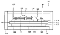
- FIG. 11 is a cross-sectional view showing a configuration example of a conventional semiconductor device.
- the illustrated semiconductor device 100 shows a configuration example of a type in which two semiconductor chips 101 and 102 are mounted.
- the semiconductor device 100 includes an insulating substrate 103.
- the insulating substrate 103 includes a ceramic plate 103a, a circuit plate 103b bonded to the front surface (upper surface in the figure) of the ceramic plate 103a, and a metal plate 103c bonded to the rear surface (lower surface in the drawing) of the ceramic plate 103a. And have.
- the semiconductor chips 101 and 102 are respectively joined by solder 104 on the circuit board 103b, and a plurality of external terminals 105 are joined by solder 104 on the circuit board 103b.
- a base plate 107 for heat dissipation is joined to the back surface of the metal plate 103c by solder 108.
- a bonding wire 109 is electrically connected between the semiconductor chip 101 and the semiconductor chip 102 and between the semiconductor chip 102 and the circuit board 103b.
- the base plate 107, the insulating substrate 103, and the semiconductor chips 101 and 102 are accommodated in a box-shaped resin case 110 whose lower end is opened. Then, the internal member is sealed by injecting resin into the resin case 110 and curing it.
- the inverter device is configured by combining a plurality of semiconductor devices as described above. At this time, it has been proposed that the connection between the plurality of semiconductor devices is performed by using a plate-like bus bar as an external terminal of each semiconductor device (see, for example, Patent Document 1).
- a plate-like bus bar is used for connection between a plurality of semiconductor devices.
- the inductance of the wiring between semiconductor devices can be reduced.
- an actual semiconductor device package has various shape requirements, so that the wiring of the bus bar is often complicated. In general, the smaller the device size, the thinner the bus bar, and thus the inductance often increases.
- the present invention has been made in view of the above points, and provides a semiconductor device capable of reducing the inductance of wiring inside the device and reducing the inductance of wiring even when connected to other semiconductor devices. Objective.
- the semiconductor device includes a first switching element and a second switching element, a first diode and a second diode, a first circuit board on which the first switching element and the first diode are mounted, A second circuit board on which a second switching element and a second diode are mounted; a printed circuit board disposed opposite to the first circuit board and the second circuit board and having a metal layer; A plurality of conductive posts for electrically connecting the switching element, the second switching element, the first diode, the second diode, the first circuit board or the second circuit board, and the metal layer of the printed circuit board And.
- the first switching element and the first diode are connected in antiparallel
- the second switching element and the second diode are connected in antiparallel
- the first switching element and the second switching element Are connected in series in opposite directions to each other via the conductive posts and the metal layer to constitute a bidirectional switch.
- the semiconductor device having the above-described configuration can reduce the inductance of wiring inside the device, and can reduce the inductance of external wiring connected to other semiconductor devices.
- FIG. 1 is a central longitudinal sectional view of a semiconductor device as a semiconductor device according to a first embodiment; It is a figure which shows the example of the wiring pattern of a semiconductor device. It is a perspective view which shows the external appearance of a semiconductor device. It is a figure which shows the usage condition of the semiconductor device which concerns on 1st Embodiment. It is a circuit diagram which shows one structural example of the three level inverter to which the semiconductor device which concerns on 2nd Embodiment is applied.
- FIG. 1 It is a figure which shows the example of the wiring pattern of the semiconductor device which comprises the intermediate
- FIG. 1 is a diagram illustrating a basic configuration of a three-level inverter device to which the semiconductor device according to the first embodiment is applied
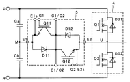
- FIG. 2 is a circuit diagram illustrating a configuration example of the three-level inverter.
- the three-level inverter device to which the semiconductor device according to the first embodiment is applied includes a DC power source 1, a conversion unit 2, and a filter unit 3.
- the conversion unit 2 includes a capacitor Ca, a capacitor Cb, an inverter 4, and an intermediate arm unit 5.
- One terminal of the capacitor Ca is connected to the positive terminal P of the DC power supply 1, and the other terminal is connected to the terminal of the capacitor Cb.
- the other terminal of the capacitor Cb is connected to the negative terminal N of the DC power supply 1.
- the inverter 4 is connected in parallel to a series connection circuit of capacitors Ca and Cb.
- the inverter 4 includes transistors Q1 and Q2 and diodes D01 and D02.
- the transistor Q1 and the diode D01 are connected in antiparallel to constitute the upper arm of the inverter 4.
- the transistor Q2 and the diode D02 are connected in antiparallel to constitute the lower arm of the inverter 4.
- the upper arm and the lower arm are connected in series to constitute the inverter 4.
- N-channel MOSFETs are used as the transistors Q1 and Q2.
- the intermediate arm unit 5 is disposed between the intermediate potential point M of the capacitors Ca and Cb and the intermediate connection point U of the transistors Q1 and Q2.
- the intermediate arm unit 5 has a configuration of a bidirectional switch made of a semiconductor element.
- the filter unit 3 connected to the conversion unit 2 includes a coil L and a capacitor C.
- One end of the coil L is connected to the intermediate connection point U of the transistors Q1 and Q2, and the other end is connected to one terminal of the capacitor C.
- This three-level inverter device is configured to always clamp the voltage applied to the transistors Q1 and Q2 of the inverter 4 to a voltage half the voltage E of the DC power source 1. Thereby, the output waveform of the inverter 4 becomes a PWM (Pulse Width Modulation) pulse in which ⁇ E / 2 and ⁇ E are combined around the zero point. Therefore, the three-level inverter can create a waveform that is closer to a sine wave than the waveform output by a general two-level inverter. And the filter part 3 for making an output waveform into a sine wave can be reduced in size.
- PWM Pulse Width Modulation
- the switching loss and switching noise of the transistors Q1 and Q2 can be reduced, and the efficiency of the switching operation can be increased.
- the semiconductor device of the present invention is applied to the intermediate arm portion 5 of the above-described three-level inverter device.
- the intermediate arm unit 5 of the first embodiment includes transistors Q11 and Q12, which are IGBTs, and diodes D11 and D12.
- Transistor Q11 has an emitter connected to terminal E1, a collector connected to terminal C1 / C2, an auxiliary emitter connected to terminal E1s, and a gate connected to terminal G1.
- the diode D11 has an anode connected to the terminal E1 and a cathode connected to the terminal C1 / C2. That is, the transistor Q11 and the diode D11 are connected in antiparallel.
- Transistor Q12 has an emitter connected to terminal E2, a collector connected to terminal C1 / C2, an auxiliary emitter connected to terminal E2s, and a gate connected to terminal G2.
- the diode D12 has an anode connected to the terminal E2 and a cathode connected to the terminal C1 / C2. That is, the transistor Q12 and the diode D12 are connected in antiparallel.
- the terminals C1 / C2 are electrically connected inside the intermediate arm portion 5. That is, the collector of the transistor Q11, the collector of the transistor Q12, the cathode of the diode D11, and the cathode of the diode D12 are all connected to the terminal C1 / C2. Thus, the transistor Q11 and the transistor Q12 are connected in series in opposite directions.
- the terminal E1 is connected to an intermediate potential point M that is a common connection point between the capacitors Ca and Cb, and the terminal E2 is connected to an intermediate connection point U that is a common connection point between the transistors Q1 and Q2. ing.
- the terminals C1 / C2 are not connected to an external circuit, but are used for checking internal wiring, element characteristics, and the like during manufacturing.
- the transistor Q11 can be switched from an off (non-conducting) state to an on (conducting) state by applying a predetermined voltage between the terminal G1 and the terminal E1s.
- the transistor Q12 can also be switched from the off state to the on state by applying a predetermined voltage to the terminal G2 and the terminal E2s.
- the terminal E1 and the terminal E2 are off.
- transistor Q11 is on and transistor Q12 is off, the series connection circuit of diode D12 and transistor Q11 is on. Therefore, the intermediate arm unit 5 can flow a current from the terminal E2 to the terminal E1.
- the intermediate arm unit 5 can flow a current from the terminal E1 to the terminal E2.
- the intermediate arm unit 5 functions as a bidirectional switch that allows a current to flow in both directions by turning one of the transistors Q11 and Q12 on and the other off. Have.
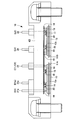
- FIG. 3 is a central longitudinal sectional view of the semiconductor device according to the first embodiment.
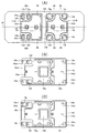
- FIG. 4 is a diagram illustrating an example of a wiring pattern of a semiconductor device. 4A shows a wiring pattern on the circuit board, FIG. 4B shows a wiring pattern on the upper surface side of the printed board, and FIG. 4C shows a wiring pattern on the lower surface side of the printed board. Note that FIG. 4C shows a wiring pattern that is reversed upside down (that is, seen through from the top side) for easy understanding.
- FIG. 5 is a perspective view showing the appearance of the semiconductor device.
- FIG. 6 is a diagram illustrating a usage pattern of the semiconductor device according to the first embodiment.
- the semiconductor device 10 includes a first switching element 14, a second switching element 16, a first diode 15, a second diode 17, a first circuit board 12a, and a second circuit board 12b.
- a printed circuit board 18 and a plurality of conductive posts 19 and 20 are provided.
- the semiconductor device 10 further includes a plurality of third circuit boards 12c, 12d, 12e, 12f, 12g, 12h, 12i, and 12j, and a plurality of external terminals 21a, 21b, 22a, 22b, 23, 24, and 25. ing.
- third circuit boards 12c to 12j when all of the above-described third circuit boards are targeted, they may be described as third circuit boards 12c to 12j.
- the semiconductor device 10 includes a first insulating substrate 11A and a second insulating substrate 11B arranged side by side in the horizontal direction.
- the first insulating substrate 11A and the second insulating substrate 11B are made of a ceramic plate such as alumina, aluminum nitride, or silicon nitride having good heat transfer, a circuit plate disposed on the upper surface, and a metal plate disposed on the lower surface. It is configured.
- the first circuit board 12a is disposed on the top surface of the first insulating substrate 11A, and the metal plate 13 having the same thickness is disposed on the back surface.
- the second circuit board 12b is disposed on the upper surface of the second insulating substrate 11B, and the metal plate 13 having the same thickness is disposed on the rear surface.
- a plurality of third circuit boards 12c to 12j are arranged on the upper surfaces of the first insulating substrate 11A and the second insulating substrate 11B.
- the first circuit board 12a, the second circuit board 12b, and the third circuit boards 12c to 12j are made of, for example, a copper plate having a thickness of 0.5 mm to 1.5 mm.
- the first switching element 14 and the first diode 15 are mounted on the first circuit board 12a.
- a second switching element 16 and a second diode 17 are mounted on the second circuit board 12b.
- the first switching element 14 and the first diode 15 correspond to the transistor Q11 and the diode D11 in FIG. 2, respectively.
- the second switching element 16 and the second diode 17 correspond to the transistor Q12 and the diode D12 in FIG. 2, respectively.
- the first switching element 14, the first diode 15, the second switching element 16, and the second diode 17 are separately mounted on two insulating substrates.
- the deformation of the insulating substrate due to thermal stress increases, which may cause the insulating substrate or resin to break or the circuit board or resin to peel from the insulating substrate. is there.
- the reliability can be improved by dividing the insulating substrate into two.
- a printed circuit board 18 is arranged facing the first circuit board 12a and the second circuit board 12b with a predetermined interval.
- the printed circuit board 18 has a metal layer having a wiring pattern shown in FIG. 4B on its upper surface and a metal layer having a wiring pattern shown in FIG. 4C on its lower surface.
- a predetermined metal layer of the printed circuit board 18 and the first circuit board 12a, the second circuit board 12b, or the third circuit boards 12c to 12j are electrically connected by a cylindrical conductive post 19. Yes.
- electrical connection between a predetermined metal layer of the printed circuit board 18 and the first switching element 14, the first diode 15, the second switching element 16, or the second diode 17 is performed by a cylindrical conductive post 20.
- external terminals 21a, 21b, 22a, 22b, 23, 24, and 25 are electrically and mechanically connected to the first circuit board 12a and the third circuit boards 12c to 12j.
- electroconductive joining materials such as a solder and a metal sintered material, can be used.
- the first circuit board 12a, the second circuit board 12b, the first switching element 14, the first diode 15, the second switching element 16, the second diode 17, the conductive posts 19, 20 and the printed circuit board 18 are It is covered with a resin such as a thermosetting epoxy resin. Then, the semiconductor device 10 as shown in FIG. 5 is formed.
- the semiconductor device 10 has a substantially rectangular parallelepiped shape made of a resin 40, and the external terminals 21a, 22a, 23, 24, 25 and the external terminals 21b, 22b, 23, 24, 25 are respectively lines with the longitudinal center line as an axis. It is arranged in a symmetrical position.
- the first insulating substrate 11A and the second insulating substrate 11B are arranged side by side in the longitudinal direction of the semiconductor device 10 as shown in FIG.
- the first circuit board 12a and the third circuit boards 12c, 12d, 12e, and 12f are disposed on the upper surface of the first insulating substrate 11A.
- the first switching element 14 and the first diode 15 are mounted, and two external terminals 23 are connected.
- External terminals 21a, 21b, 22a, and 22b are connected to the third circuit boards 12c, 12d, 12e, and 12f, respectively.
- the second circuit board 12b and the third circuit boards 12g, 12h, 12i, and 12j are disposed on the upper surface of the second insulating substrate 11B.
- a second switching element 16 and a second diode 17 are mounted on the second circuit board 12b.
- Two external terminals 24 and 25 are connected to each of the third circuit boards 12g, 12h, 12i, and 12j.
- the first circuit board 12a and the second circuit board 12b have a line-symmetric shape about a center line 41 extending in the direction in which the first insulating substrate 11A and the second insulating substrate 11B are arranged.
- the plurality of third circuit boards 12 c to 12 j are arranged side by side at positions symmetrical with respect to the center line 41. Further, the switching element 14, the first diode 15, the second switching element 16 and the second diode 17 are disposed on the center line 41.
- the first switching element 14 and the second switching element 16 which are IGBTs include an emitter electrode and a gate electrode on the front surface, and a collector electrode on the back surface.
- the collector electrode of the first switching element 14 is electrically and mechanically connected to the first circuit board 12a
- the collector electrode of the second switching element 16 is electrically and mechanically connected to the second circuit board 12b. Connected.
- the first diode 15 and the second diode 17 have an anode electrode on the front surface and a cathode electrode on the back surface.
- the cathode electrode of the first diode 15 is electrically and mechanically connected to the second circuit board 12b.
- the first circuit board 12a, the second circuit board 12b, and the plurality of third circuit boards 12c to 12j have a plurality of connection points 12k that are connected to the printed circuit board 18 by the conductive posts 19.
- metal layers 18a, 18b, 18c, 18d, 18e, and 18f are arranged on the upper surface side of the printed circuit board 18.
- the metal layers 18a, 18b and 18c are metal layers for the main circuit
- the metal layers 18d and 18e are metal layers for the gate circuit
- the metal layer 18f is a metal layer for terminal connection.
- metal layers 18g, 18h, 18i, 18j, 18k, and 18l are arranged on the lower surface side of the printed circuit board 18.
- the metal layers 18g, 18h, and 18i are metal layers for main circuits
- the metal layer 18j is a metal layer for terminal connection
- the metal layers 18k and 18l are metal layers for auxiliary emitters.
- the metal layers 18g and 18i are electrically connected to each other.
- the printed circuit board 18 has a plurality of through holes 18m.
- the positions of the plurality of through holes 18m are the positions of the plurality of connection points 12k, the electrodes of the first switching element 14, the electrodes of the first diode 15, the electrodes of the second switching element 16, and the electrodes of the second diode 17. It corresponds to each.
- the printed circuit board 18 is provided with through holes 18n corresponding to positions where the external terminals 21a, 21b, 22a, 22b, 23, 24, 25 are connected.
- the collector electrode of the first switching element 14 is connected to the external terminal 23 (terminal C1 / C2) via the first circuit board 12a.
- the emitter electrode of the first switching element 14 is first connected to the metal layers 18a and 18g of the printed circuit board 18 via the conductive post 20, and then the conductive post 19 and the third circuit board 12g (or the third circuit board 12g).
- the circuit board 12h) is connected to the external terminal 24 (terminal E1).
- the gate electrode of the first switching element 14 is first connected to the metal layer 18d via the conductive post 20, and then to the external terminal 21a (terminal) via the conductive post 19 and the third circuit board 12c. G1).
- the auxiliary emitter electrode of the first switching element 14 is first connected to the metal layer 18g through the conductive post 20, and then through the metal layer 18k, the conductive post 19 and the third circuit board 12e, It is connected to the external terminal 22a (terminal E1s).
- the cathode electrode of the first diode 15 is connected to the external terminal 23 (terminal C1 / C2) via the first circuit board 12a.
- the anode electrode of the first diode 15 is first connected to the metal layers 18a and 18g via the conductive post 20, and then the conductive post 19 and the third circuit board 12g (or the third circuit board 12h).
- the collector electrode of the second switching element 16 is first connected to the metal layers 18b and 18h via the second circuit board 12b and the conductive post 19, and then the conductive post 19 and the first circuit board 12a are connected. Via, it is connected to the external terminal 23 (terminal C1 / C2). That is, the metal layers 18b and 18h serve as a bridge that forms a collector current path between the separated first insulating substrate 11A and the second insulating substrate 11B.
- the emitter electrode of the second switching element 16 is first connected to the metal layers 18c and 18i via the conductive post 20, and then the conductive post 19 and the third circuit board 12i (or the third circuit board 12j). ) To the external terminal 25 (terminal E2).
- the gate electrode of the second switching element 16 is first connected to the metal layer 18e via the conductive post 20, and then to the external terminal 21b (terminal) via the conductive post 19 and the third circuit board 12d. G2).
- the auxiliary emitter electrode of the second switching element 16 is first connected to the metal layer 18i through the conductive post 20, and then through the metal layer 18l, the conductive post 19 and the third circuit board 12f, Connected to the external terminal 22b (terminal E2s).
- the cathode electrode of the second diode 17 is first connected to the metal layers 18b and 18h via the second circuit board 12b and the conductive post 19, and then via the conductive post 19 and the first circuit board 12a. Then, it is connected to the external terminal 23 (terminal C1 / C2).
- the anode electrode of the second diode 17 is first connected to the metal layers 18c and 18i via the conductive post 20, and then the conductive post 19 and the third circuit board 12i (or the third circuit board 12j).
- terminal E2 terminal E2
- the wiring inside the semiconductor device is configured by the printed circuit board 18 and the conductive posts 19 and 20.
- the current path is thicker and shorter than the bonding wire used in the semiconductor device 100 of the conventional example, so that the wiring inductance can be greatly reduced.
- a semiconductor device compatible with high-speed switching can be realized.
- FIG. 6A shows an example in which two semiconductor devices 10 are juxtaposed and connected in parallel by bus bars 26, 27, 28 to configure the intermediate arm unit 5 having a large capacity.
- two external terminals 23, 24, and 25 are arranged side by side in the short direction of the semiconductor device 10. Accordingly, even when a plurality of external terminals 23, 24, and 25 are connected in parallel, the external terminals 23, 24, and 25 can be arranged in a straight line. Therefore, the bus bars 26, 27, and 28 can be formed in the shortest straight line. .
- the inductance of the external wiring can be reduced, and a semiconductor device with a large current capacity corresponding to high-speed switching can be realized.
- FIG. 6B an example in which the inverter 4 and the intermediate arm portion 5 shown in FIG. 2 are formed in the same package shape, and the semiconductor device 4a of the inverter 4 and the semiconductor device 10 of the intermediate arm portion 5 are combined.
- the semiconductor device 4a of the inverter 4 external terminals are arranged in the order of the gates and auxiliary source terminals of the transistors Q1 and Q2, the positive terminal P, the negative terminal N, and the intermediate connection point U from the lower side of the figure.
- the semiconductor device 4 a of the inverter 4 and the semiconductor device 10 of the intermediate arm unit 5 are arranged side by side in the short direction, and are connected by a bus bar 29 and a laminate bus bar 30.
- the bus bar 29 wires the external terminal 25 (terminal E2) of the semiconductor device 10 and the intermediate connection point U of the semiconductor device 4a at the shortest distance.
- the laminate bus bar 30 is formed by laminating four metal conductors and an insulating film sheet.
- the laminate bus bar 30 includes a bus bar 30a connected to the terminals C1 / C2, a bus bar 30b connected to the positive terminal P, a bus bar 30c connected to the intermediate potential point M, and a bus bar 30d connected to the negative terminal N.
- the bus bar 30a is connected to the external terminal 23 of the semiconductor device 10, and the bus bar 30b is connected to the positive terminal P of the semiconductor device 4a.
- the bus bar 30c is connected to the external terminal 24 of the semiconductor device 10, and the bus bar 30d is connected to the negative terminal N of the semiconductor device 4a.
- the semiconductor device 4 a of the inverter 4 and the semiconductor device 10 of the intermediate arm unit 5 are wired at the shortest distance by the bus bar 29 and the laminate bus bar 30.
- the inductance of the external wiring is also reduced.
- the laminated bus bar 30 composed of multiple layers can be applied, the mutual inductance of external wiring can also be reduced. Thereby, the three-level inverter device corresponding to high-speed switching can be provided.
- first switching element 14 the first diode 15, the second switching element 16, and the second diode 17 are mounted one by one.
- a plurality of first switching elements 14, first diodes 15, second switching elements 16, and second diodes 17 may be provided in parallel depending on the required current capacity.
- the first switching element 14, the first diode 15, the second switching element 16, and the second diode 17 may be made of a silicon semiconductor, SiC (silicon carbide), GaN (gallium nitride). ) Or a wide band gap semiconductor such as diamond.
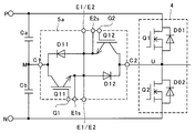
- FIG. 7 is a circuit diagram showing a configuration of a three-level inverter to which the semiconductor device according to the second embodiment is applied.
- FIG. 8 is a diagram illustrating an example of a wiring pattern of the semiconductor device constituting the intermediate arm portion shown in FIG. 8A shows a wiring pattern on the circuit board
- FIG. 8B shows a wiring pattern on the upper surface side of the printed board
- FIG. 8C shows a wiring pattern on the lower surface side of the printed board. Note that FIG. 8C shows a wiring pattern that is reversed upside down (that is, seen through from the upper surface side) for easy understanding.
- the intermediate arm unit 5a which is a semiconductor device according to the second embodiment, uses the same components as those of the intermediate arm unit 5 according to the first embodiment, but the circuit configuration is changed. That is, the intermediate arm unit 5 according to the first embodiment has a circuit configuration in which the collectors of the transistors Q11 and Q12 are connected to each other, whereas the intermediate arm unit 5a according to the second embodiment includes a transistor configuration. The circuit configuration is such that the emitters of Q11 and Q12 are connected to each other. Details are described below.
- Transistor Q11 has an emitter connected to terminal E1 / E2, a collector connected to terminal C1, an auxiliary emitter connected to terminal E1s, and a gate connected to terminal G1.
- the diode D11 has an anode connected to the terminal E1 / E2 and a cathode connected to the terminal C1. That is, the transistor Q11 and the diode D11 are connected in antiparallel.
- Transistor Q12 has an emitter connected to terminal E1 / E2, a collector connected to terminal C2, an auxiliary emitter connected to terminal E2s, and a gate connected to terminal G2.
- the diode D12 has an anode connected to the terminal E1 / E2 and a cathode connected to the terminal C2. That is, the transistor Q12 and the diode D12 are connected in antiparallel.
- the terminals E1 / E2 are electrically connected inside the intermediate arm portion 5a. That is, the emitter of the transistor Q11, the emitter of the transistor Q12, the anode of the diode D11, and the anode of the diode D12 are all connected to the terminal E1 / E2. Thus, the transistor Q11 and the transistor Q12 are connected in series in opposite directions.
- the terminal C1 is connected to an intermediate potential point M that is a common connection point between the capacitors Ca and Cb, and the terminal C2 is connected to an intermediate connection point U that is a common connection point between the transistors Q1 and Q2. ing.
- the intermediate arm unit 5a is capable of flowing a current in both directions by setting one of the transistors Q11 and Q12 to an on state and the other to an off state, as in the first embodiment. It has the structure as a direction switch.
- the external terminals 23, 24, and 25 are connected to terminals different from those in the first embodiment. That is, the external terminal 23 is connected to the common emitter terminal E1 / E2 of the transistors Q11 and Q12, the external terminal 24 is connected to the collector terminal C1 of the transistor Q11, and the external terminal 25 is the collector of the transistor Q12. Connected to terminal C2.
- the collector electrode of the first switching element 14 corresponding to the transistor Q11 is first connected to the metal layers 18b and 18h via the first circuit board 12a and the conductive post 19, and then the conductive post 19 and the third
- the circuit board 12i (or the third circuit board 12j) is connected to the external terminal 24 (terminal C1).
- the emitter electrode of the first switching element 14 is first connected to the metal layers 18a and 18g via the conductive post 20, and then the conductive post 19 and the third circuit board 12g (or the third circuit board 12h).
- To the external terminal 23 terminal E1 / E2).
- the gate electrode of the first switching element 14 is first connected to the metal layer 18d via the conductive post 20, and then to the external terminal 21a (terminal) via the conductive post 19 and the third circuit board 12c. G1).
- the auxiliary emitter electrode of the first switching element 14 is first connected to the metal layer 18g via the conductive post 20, and then to the third circuit via the metal layer 18g, the metal layer 18k, and the conductive post 19. It is connected to the external terminal 22a (terminal E1s) via the plate 12e.
- the cathode electrode of the first diode 15 corresponding to the diode D11 is first connected to the metal layers 18b and 18h via the first circuit board 12a and the conductive post 19, and then the conductive post 19 and the third It is connected to the external terminal 24 (terminal C1) via the circuit board 12i (or the third circuit board 12j).
- the anode electrode of the first diode 15 is first connected to the metal layers 18a and 18g via the conductive post 20, and then the conductive post 19 and the third circuit board 12g (or the third circuit board 12h).
- the collector electrode of the second switching element 16 corresponding to the transistor Q12 is connected to the external terminal 25 (terminal C2) via the second circuit board 12b.
- the emitter electrode of the second switching element 16 is first connected to the metal layer 18i via the conductive post 20, and then the metal layer 18g, the conductive post 19 and the third circuit board 12g (or the third circuit). It is connected to the external terminal 23 (terminal E1 / E2) via the board 12h).
- the gate electrode of the second switching element 16 is first connected to the metal layer 18e via the conductive post 20, and then to the external terminal 21b (terminal) via the conductive post 19 and the third circuit board 12d. G2).
- the auxiliary emitter electrode of the second switching element 16 is first connected to the metal layer 18i through the conductive post 20, and then through the metal layer 18l, the conductive post 19 and the third circuit board 12f, Connected to the external terminal 22b (terminal E2s).
- the cathode electrode of the second diode 17 corresponding to the diode D12 is connected to the external terminal 25 (terminal C2) via the second circuit board 12b.
- the anode electrode of the second diode 17 is first connected to the metal layer 18i via the conductive post 20, and then the metal layer 18g, the conductive post 19 and the third circuit board 12g (or the third circuit board). 12h) and connected to the external terminal 23 (terminal E1 / E2).
- the wiring inside the semiconductor device is configured by the printed circuit board 18 and the conductive posts 19 and 20 as in the first embodiment.
- the current path is thicker and shorter than the bonding wire used in the conventional semiconductor device 100, so that the wiring inductance can be greatly reduced.
- a semiconductor device compatible with high-speed switching can be realized.
- FIG. 9 is a circuit diagram showing a configuration example of a three-level inverter to which the semiconductor device according to the third embodiment is applied.
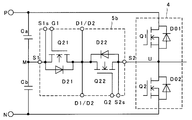
- the transistor of the intermediate arm unit 5 of the first embodiment is changed from the IGBT to the power MOSFET. That is, the intermediate arm portion 5b includes transistors Q21 and Q22, which are power MOSFETs, and diodes D21 and D22. Therefore, in the following description, the same or equivalent components as those shown in the first embodiment are denoted by the same reference numerals, and detailed description thereof is omitted.
- Transistor Q21 has a source connected to terminal S1, a drain connected to terminal D1 / D2, an auxiliary source connected to terminal S1s, and a gate connected to terminal G1.
- the diode D21 has an anode connected to the terminal S1 and a cathode connected to the terminal D1 / D2. That is, the transistor Q21 and the diode D21 are connected in antiparallel.
- Transistor Q22 has a source connected to terminal S2, a drain connected to terminal D1 / D2, an auxiliary source connected to terminal S2s, and a gate connected to terminal G2.
- the diode D22 has an anode connected to the terminal S2 and a cathode connected to the terminal D1 / D2. That is, the transistor Q22 and the diode D22 are connected in antiparallel.
- the terminals D1 / D2 are electrically connected inside the intermediate arm portion 5b. That is, the drain of the transistor Q21, the drain of the transistor Q22, the cathode of the diode D21, and the cathode of the diode D22 are all connected to the terminal D1 / D2. In this way, the transistor Q21 and the transistor Q22 are connected in series in opposite directions.
- a terminal S1 is connected to an intermediate potential point M that is a common connection point between the capacitors Ca and Cb, and a terminal S2 is connected to an intermediate connection point U that is a common connection point between the transistors Q1 and Q2. ing.
- the intermediate arm portion 5b functions as a bidirectional switch by turning one of the transistors Q21 and Q22 on and the other off.
- the intermediate arm portion 5b has the same configuration as the intermediate arm portion 5 of the first embodiment.
- the first circuit board 12a, the second circuit board 12b, and the printed circuit board 18 can be the same as those shown in the first embodiment.
- FIG. 10 is a circuit diagram showing a configuration example of a three-level inverter to which the semiconductor device according to the fourth embodiment is applied.
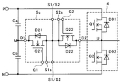
- the transistor of the intermediate arm unit 5a of the second embodiment is changed from an IGBT to a power MOSFET. That is, the intermediate arm portion 5c includes transistors Q21 and Q22, which are power MOSFETs, and diodes D21 and D22. Therefore, in the following description, the same or equivalent components as those shown in the second embodiment are denoted by the same reference numerals, and detailed description thereof is omitted.
- Transistor Q21 has a source connected to terminal S1 / S2, a drain connected to terminal D1, an auxiliary source connected to terminal S1s, and a gate connected to terminal G1.
- the diode D21 has an anode connected to the terminals S1 / S2 and a cathode connected to the terminal D1. That is, the transistor Q21 and the diode D21 are connected in antiparallel.
- Transistor Q22 has a source connected to terminal S1 / S2, a drain connected to terminal D2, an auxiliary source connected to terminal S2s, and a gate connected to terminal G2.
- the diode D22 has an anode connected to the terminal S1 / S2 and a cathode connected to the terminal D2. That is, the transistor Q22 and the diode D22 are connected in antiparallel.
- the terminals S1 / S2 are electrically connected inside the intermediate arm portion 5c. That is, the source of the transistor Q21, the source of the transistor Q22, the anode of the diode D21, and the anode of the diode D22 are all connected to the terminals S1 / S2. In this way, the transistor Q21 and the transistor Q22 are connected in series in opposite directions.
- a terminal D1 is connected to an intermediate potential point M that is a common connection point between the capacitors Ca and Cb, and a terminal D2 is connected to an intermediate connection point U that is a common connection point between the transistors Q1 and Q2. ing.
- the intermediate arm portion 5c functions as a bidirectional switch by turning one of the transistors Q21 and Q22 on and the other off.
- the intermediate arm portion 5c has the same configuration as the intermediate arm portion 5a of the second embodiment. For this reason, the same thing as what was shown in 1st Embodiment can be used for the 1st circuit board 12a, the 2nd circuit board 12b, and the printed circuit board 18.
- FIG. 1st Embodiment can be used for the 1st circuit board 12a, the 2nd circuit board 12b, and the printed circuit board 18.
Landscapes
- Engineering & Computer Science (AREA)
- Microelectronics & Electronic Packaging (AREA)
- Chemical & Material Sciences (AREA)
- Ceramic Engineering (AREA)
- Inorganic Chemistry (AREA)
- Inverter Devices (AREA)
Abstract
Priority Applications (5)
| Application Number | Priority Date | Filing Date | Title |
|---|---|---|---|
| DE112015000156.5T DE112015000156T5 (de) | 2014-04-14 | 2015-04-06 | Halbleitervorrichtung |
| JP2016513724A JP6202195B2 (ja) | 2014-04-14 | 2015-04-06 | 半導体装置 |
| CN201580002148.1A CN105612690B (zh) | 2014-04-14 | 2015-04-06 | 半导体装置 |
| US15/091,564 US10187973B2 (en) | 2014-04-14 | 2016-04-05 | Semiconductor device |
| US16/249,391 US10398023B2 (en) | 2014-04-14 | 2019-01-16 | Semiconductor device |
Applications Claiming Priority (2)
| Application Number | Priority Date | Filing Date | Title |
|---|---|---|---|
| JP2014082651 | 2014-04-14 | ||
| JP2014-082651 | 2014-04-14 |
Related Child Applications (1)
| Application Number | Title | Priority Date | Filing Date |
|---|---|---|---|
| US15/091,564 Continuation US10187973B2 (en) | 2014-04-14 | 2016-04-05 | Semiconductor device |
Publications (1)
| Publication Number | Publication Date |
|---|---|
| WO2015159751A1 true WO2015159751A1 (fr) | 2015-10-22 |
Family
ID=54323962
Family Applications (1)
| Application Number | Title | Priority Date | Filing Date |
|---|---|---|---|
| PCT/JP2015/060743 Ceased WO2015159751A1 (fr) | 2014-04-14 | 2015-04-06 | Dispositif à semi-conducteur |
Country Status (5)
| Country | Link |
|---|---|
| US (2) | US10187973B2 (fr) |
| JP (1) | JP6202195B2 (fr) |
| CN (1) | CN105612690B (fr) |
| DE (1) | DE112015000156T5 (fr) |
| WO (1) | WO2015159751A1 (fr) |
Cited By (4)
| Publication number | Priority date | Publication date | Assignee | Title |
|---|---|---|---|---|
| JP2021191156A (ja) * | 2020-06-02 | 2021-12-13 | 富士電機株式会社 | 電力変換装置 |
| CN115497917A (zh) * | 2022-08-05 | 2022-12-20 | 北京智慧能源研究院 | 一种碳化硅芯片封装结构 |
| JP2023080469A (ja) * | 2021-11-30 | 2023-06-09 | 三菱電機株式会社 | 半導体装置 |
| JP7771523B2 (ja) | 2021-04-07 | 2025-11-18 | 富士電機株式会社 | 電力変換装置 |
Families Citing this family (14)
| Publication number | Priority date | Publication date | Assignee | Title |
|---|---|---|---|---|
| WO2014185050A1 (fr) * | 2013-05-16 | 2014-11-20 | 富士電機株式会社 | Dispositif à semi-conducteur |
| DE102015216047A1 (de) * | 2015-08-21 | 2017-02-23 | Continental Automotive Gmbh | Schaltungsträger, Leistungselektronikanordnung mit einem Schaltungsträger |
| DE102017100530A1 (de) * | 2017-01-12 | 2018-07-12 | Danfoss Silicon Power Gmbh | Drei-Stufen-Leistungsmodul |
| JP6740959B2 (ja) * | 2017-05-17 | 2020-08-19 | 株式会社オートネットワーク技術研究所 | 回路装置 |
| DE102017209515A1 (de) * | 2017-06-06 | 2018-12-06 | Bayerische Motoren Werke Aktiengesellschaft | Leistungsumrichtermodul und Verfahren zu dessen Herstellung |
| JP2019068648A (ja) * | 2017-10-02 | 2019-04-25 | 株式会社豊田自動織機 | インバータ装置 |
| CN108566110A (zh) * | 2018-02-02 | 2018-09-21 | 山东理工大学 | 一种t形有源中点箝位光伏逆变电路及其控制方法 |
| JP6687053B2 (ja) * | 2018-03-29 | 2020-04-22 | ダイキン工業株式会社 | 半導体装置 |
| EP4097761B1 (fr) | 2020-01-30 | 2024-06-26 | Hitachi Energy Ltd | Module semi-conducteur de puissance configurable librement |
| EP3944312A1 (fr) * | 2020-07-23 | 2022-01-26 | Siemens Aktiengesellschaft | Module électronique de puissance |
| DE102022213626A1 (de) * | 2022-12-14 | 2024-06-20 | Robert Bosch Gesellschaft mit beschränkter Haftung | Leistungsmodul |
| TWI830566B (zh) | 2022-12-30 | 2024-01-21 | 恆勁科技股份有限公司 | 整合有電感線路結構之封裝載板及其製造方法 |
| DE102023126065A1 (de) * | 2023-09-26 | 2025-03-27 | Semikron Elektronik Gmbh & Co. Kg | Drei-Level-Leistungshalbleitermodul und Anordnung hiermit |
| DE102024203650A1 (de) * | 2024-04-19 | 2025-10-23 | Robert Bosch Gesellschaft mit beschränkter Haftung | Invertereinheit |
Citations (8)
| Publication number | Priority date | Publication date | Assignee | Title |
|---|---|---|---|---|
| JP2000295864A (ja) * | 1999-04-05 | 2000-10-20 | Toshiba Corp | 電力変換装置 |
| JP2008193779A (ja) * | 2007-02-02 | 2008-08-21 | Fuji Electric Systems Co Ltd | 半導体モジュール |
| JP2009064852A (ja) * | 2007-09-05 | 2009-03-26 | Okutekku:Kk | 半導体装置及び半導体装置の製造方法 |
| JP2012119618A (ja) * | 2010-12-03 | 2012-06-21 | Fuji Electric Co Ltd | パワー半導体モジュール |
| WO2013118415A1 (fr) * | 2012-02-09 | 2013-08-15 | 富士電機株式会社 | Dispositif à semiconducteur |
| WO2013145620A1 (fr) * | 2012-03-28 | 2013-10-03 | 富士電機株式会社 | Dispositif à semi-conducteur |
| JP2013215042A (ja) * | 2012-04-02 | 2013-10-17 | Fuji Electric Co Ltd | 3レベル電力変換装置 |
| JP2013222950A (ja) * | 2012-04-19 | 2013-10-28 | Fuji Electric Co Ltd | パワー半導体モジュール |
Family Cites Families (12)
| Publication number | Priority date | Publication date | Assignee | Title |
|---|---|---|---|---|
| JP4471967B2 (ja) * | 2006-12-28 | 2010-06-02 | 株式会社ルネサステクノロジ | 双方向スイッチモジュール |
| KR101013440B1 (ko) * | 2008-07-01 | 2011-02-14 | 삼성전자주식회사 | 지에스엠 시스템에서 핸드오버시 이중 전송 모드를유지하기 위한 방법 및 장치 |
| JP2009117868A (ja) * | 2009-02-23 | 2009-05-28 | Hitachi Ltd | 双方向スイッチモジュール |
| WO2011125367A1 (fr) * | 2010-04-06 | 2011-10-13 | シャープ株式会社 | Élément optique, et structure anti-réfléchissante et procédé pour leur production |
| JP2012005301A (ja) * | 2010-06-18 | 2012-01-05 | Fuji Electric Co Ltd | パワー半導体モジュール |
| EP2833405A4 (fr) | 2012-03-28 | 2016-01-13 | Fuji Electric Co Ltd | Dispositif à semi-conducteurs, et procédé de fabrication de celui-ci |
| JP5831626B2 (ja) | 2012-03-28 | 2015-12-09 | 富士電機株式会社 | 半導体装置及び半導体装置の製造方法 |
| GB2498236B (en) * | 2012-07-31 | 2013-12-11 | Dan Ibrahim Fogbel | Session management procedures for transferring data |
| EP2908338A4 (fr) | 2012-10-15 | 2016-07-13 | Fuji Electric Co Ltd | Dispositif à semi-conducteurs |
| WO2014185050A1 (fr) * | 2013-05-16 | 2014-11-20 | 富士電機株式会社 | Dispositif à semi-conducteur |
| US10123443B2 (en) * | 2014-12-25 | 2018-11-06 | Fuji Electric Co., Ltd. | Semiconductor device |
| JP6701641B2 (ja) * | 2015-08-13 | 2020-05-27 | 富士電機株式会社 | 半導体モジュール |
-
2015
- 2015-04-06 WO PCT/JP2015/060743 patent/WO2015159751A1/fr not_active Ceased
- 2015-04-06 JP JP2016513724A patent/JP6202195B2/ja not_active Expired - Fee Related
- 2015-04-06 CN CN201580002148.1A patent/CN105612690B/zh not_active Expired - Fee Related
- 2015-04-06 DE DE112015000156.5T patent/DE112015000156T5/de not_active Withdrawn
-
2016
- 2016-04-05 US US15/091,564 patent/US10187973B2/en not_active Expired - Fee Related
-
2019
- 2019-01-16 US US16/249,391 patent/US10398023B2/en not_active Expired - Fee Related
Patent Citations (8)
| Publication number | Priority date | Publication date | Assignee | Title |
|---|---|---|---|---|
| JP2000295864A (ja) * | 1999-04-05 | 2000-10-20 | Toshiba Corp | 電力変換装置 |
| JP2008193779A (ja) * | 2007-02-02 | 2008-08-21 | Fuji Electric Systems Co Ltd | 半導体モジュール |
| JP2009064852A (ja) * | 2007-09-05 | 2009-03-26 | Okutekku:Kk | 半導体装置及び半導体装置の製造方法 |
| JP2012119618A (ja) * | 2010-12-03 | 2012-06-21 | Fuji Electric Co Ltd | パワー半導体モジュール |
| WO2013118415A1 (fr) * | 2012-02-09 | 2013-08-15 | 富士電機株式会社 | Dispositif à semiconducteur |
| WO2013145620A1 (fr) * | 2012-03-28 | 2013-10-03 | 富士電機株式会社 | Dispositif à semi-conducteur |
| JP2013215042A (ja) * | 2012-04-02 | 2013-10-17 | Fuji Electric Co Ltd | 3レベル電力変換装置 |
| JP2013222950A (ja) * | 2012-04-19 | 2013-10-28 | Fuji Electric Co Ltd | パワー半導体モジュール |
Cited By (5)
| Publication number | Priority date | Publication date | Assignee | Title |
|---|---|---|---|---|
| JP2021191156A (ja) * | 2020-06-02 | 2021-12-13 | 富士電機株式会社 | 電力変換装置 |
| JP7771523B2 (ja) | 2021-04-07 | 2025-11-18 | 富士電機株式会社 | 電力変換装置 |
| JP2023080469A (ja) * | 2021-11-30 | 2023-06-09 | 三菱電機株式会社 | 半導体装置 |
| JP7542511B2 (ja) | 2021-11-30 | 2024-08-30 | 三菱電機株式会社 | 半導体装置 |
| CN115497917A (zh) * | 2022-08-05 | 2022-12-20 | 北京智慧能源研究院 | 一种碳化硅芯片封装结构 |
Also Published As
| Publication number | Publication date |
|---|---|
| JPWO2015159751A1 (ja) | 2017-04-13 |
| JP6202195B2 (ja) | 2017-09-27 |
| CN105612690B (zh) | 2018-11-09 |
| US20160219689A1 (en) | 2016-07-28 |
| US20190150268A1 (en) | 2019-05-16 |
| DE112015000156T5 (de) | 2016-06-16 |
| CN105612690A (zh) | 2016-05-25 |
| US10398023B2 (en) | 2019-08-27 |
| US10187973B2 (en) | 2019-01-22 |
Similar Documents
| Publication | Publication Date | Title |
|---|---|---|
| JP6202195B2 (ja) | 半導体装置 | |
| JP6366612B2 (ja) | 電力用半導体モジュール | |
| US9196572B2 (en) | Power semiconductor module | |
| US10720378B2 (en) | Component structure, power module and power module assembly structure | |
| US10153708B2 (en) | Three-level power converter | |
| JP6717270B2 (ja) | 半導体モジュール | |
| CN103296016B (zh) | 半导体模块 | |
| US11490516B2 (en) | Power module structure | |
| JPWO2013128787A1 (ja) | 電力用半導体モジュール及び電力変換装置 | |
| JPWO2015121900A1 (ja) | 電力用半導体モジュール | |
| CN104124877A (zh) | 三级变流器半桥 | |
| JP6053668B2 (ja) | 半導体モジュールおよび電力変換装置 | |
| CN105934824A (zh) | 电力用半导体装置 | |
| JP2016523069A (ja) | パワーモジュール、電力変換装置及びパワーモジュールを備えた駆動装置 | |
| CN110739294B (zh) | 功率模块结构 | |
| JP2020053622A (ja) | パワーモジュール及びパワーモジュールを有する電気装置 | |
| KR20140131279A (ko) | 서브유니트를 포함하는 전력 반도체 모듈 및 이를 포함하는 장치 | |
| JP6480856B2 (ja) | 半導体モジュール | |
| JP4349364B2 (ja) | 半導体装置 | |
| CN109585436B (zh) | 一种穿插分支布局的功率模块 | |
| CN109560066A (zh) | 一种具有过桥导电层的功率模块 | |
| JP5880664B1 (ja) | 半導体装置 | |
| JP2007053371A (ja) | ライン要素を備えたパワー半導体モジュール | |
| JP2008054495A (ja) | 電流印加されたパワー回路のための低インダクタンスのパワー半導体モジュール | |
| JP5880663B1 (ja) | 半導体装置 |
Legal Events
| Date | Code | Title | Description |
|---|---|---|---|
| 121 | Ep: the epo has been informed by wipo that ep was designated in this application |
Ref document number: 15779934 Country of ref document: EP Kind code of ref document: A1 |
|
| ENP | Entry into the national phase |
Ref document number: 2016513724 Country of ref document: JP Kind code of ref document: A |
|
| WWE | Wipo information: entry into national phase |
Ref document number: 1120150001565 Country of ref document: DE Ref document number: 112015000156 Country of ref document: DE |
|
| 122 | Ep: pct application non-entry in european phase |
Ref document number: 15779934 Country of ref document: EP Kind code of ref document: A1 |