EP3338314B1 - Mit metallamiden dotierte triarylamindickschicht zur verwendung als lochinjektionsschicht für eine organische leuchtdiode (oled) - Google Patents
Mit metallamiden dotierte triarylamindickschicht zur verwendung als lochinjektionsschicht für eine organische leuchtdiode (oled) Download PDFInfo
- Publication number
- EP3338314B1 EP3338314B1 EP16760402.4A EP16760402A EP3338314B1 EP 3338314 B1 EP3338314 B1 EP 3338314B1 EP 16760402 A EP16760402 A EP 16760402A EP 3338314 B1 EP3338314 B1 EP 3338314B1
- Authority
- EP
- European Patent Office
- Prior art keywords
- formula
- hole injection
- charge neutral
- injection layer
- amide compound
- Prior art date
- Legal status (The legal status is an assumption and is not a legal conclusion. Google has not performed a legal analysis and makes no representation as to the accuracy of the status listed.)
- Active
Links
Images


Classifications
-
- H—ELECTRICITY
- H10—SEMICONDUCTOR DEVICES; ELECTRIC SOLID-STATE DEVICES NOT OTHERWISE PROVIDED FOR
- H10K—ORGANIC ELECTRIC SOLID-STATE DEVICES
- H10K50/00—Organic light-emitting devices
- H10K50/10—OLEDs or polymer light-emitting diodes [PLED]
- H10K50/17—Carrier injection layers
-
- H—ELECTRICITY
- H10—SEMICONDUCTOR DEVICES; ELECTRIC SOLID-STATE DEVICES NOT OTHERWISE PROVIDED FOR
- H10K—ORGANIC ELECTRIC SOLID-STATE DEVICES
- H10K50/00—Organic light-emitting devices
- H10K50/10—OLEDs or polymer light-emitting diodes [PLED]
- H10K50/14—Carrier transporting layers
- H10K50/15—Hole transporting layers
- H10K50/157—Hole transporting layers between the light-emitting layer and the cathode
-
- H—ELECTRICITY
- H10—SEMICONDUCTOR DEVICES; ELECTRIC SOLID-STATE DEVICES NOT OTHERWISE PROVIDED FOR
- H10K—ORGANIC ELECTRIC SOLID-STATE DEVICES
- H10K50/00—Organic light-emitting devices
- H10K50/10—OLEDs or polymer light-emitting diodes [PLED]
- H10K50/14—Carrier transporting layers
- H10K50/16—Electron transporting layers
- H10K50/167—Electron transporting layers between the light-emitting layer and the anode
-
- H—ELECTRICITY
- H10—SEMICONDUCTOR DEVICES; ELECTRIC SOLID-STATE DEVICES NOT OTHERWISE PROVIDED FOR
- H10K—ORGANIC ELECTRIC SOLID-STATE DEVICES
- H10K85/00—Organic materials used in the body or electrodes of devices covered by this subclass
- H10K85/30—Coordination compounds
- H10K85/321—Metal complexes comprising a group IIIA element, e.g. Tris (8-hydroxyquinoline) gallium [Gaq3]
-
- H—ELECTRICITY
- H10—SEMICONDUCTOR DEVICES; ELECTRIC SOLID-STATE DEVICES NOT OTHERWISE PROVIDED FOR
- H10K—ORGANIC ELECTRIC SOLID-STATE DEVICES
- H10K85/00—Organic materials used in the body or electrodes of devices covered by this subclass
- H10K85/30—Coordination compounds
- H10K85/371—Metal complexes comprising a group IB metal element, e.g. comprising copper, gold or silver
-
- H—ELECTRICITY
- H10—SEMICONDUCTOR DEVICES; ELECTRIC SOLID-STATE DEVICES NOT OTHERWISE PROVIDED FOR
- H10K—ORGANIC ELECTRIC SOLID-STATE DEVICES
- H10K85/00—Organic materials used in the body or electrodes of devices covered by this subclass
- H10K85/60—Organic compounds having low molecular weight
- H10K85/631—Amine compounds having at least two aryl rest on at least one amine-nitrogen atom, e.g. triphenylamine
-
- H—ELECTRICITY
- H10—SEMICONDUCTOR DEVICES; ELECTRIC SOLID-STATE DEVICES NOT OTHERWISE PROVIDED FOR
- H10K—ORGANIC ELECTRIC SOLID-STATE DEVICES
- H10K85/00—Organic materials used in the body or electrodes of devices covered by this subclass
- H10K85/60—Organic compounds having low molecular weight
- H10K85/631—Amine compounds having at least two aryl rest on at least one amine-nitrogen atom, e.g. triphenylamine
- H10K85/633—Amine compounds having at least two aryl rest on at least one amine-nitrogen atom, e.g. triphenylamine comprising polycyclic condensed aromatic hydrocarbons as substituents on the nitrogen atom
-
- H—ELECTRICITY
- H10—SEMICONDUCTOR DEVICES; ELECTRIC SOLID-STATE DEVICES NOT OTHERWISE PROVIDED FOR
- H10K—ORGANIC ELECTRIC SOLID-STATE DEVICES
- H10K85/00—Organic materials used in the body or electrodes of devices covered by this subclass
- H10K85/60—Organic compounds having low molecular weight
- H10K85/649—Aromatic compounds comprising a hetero atom
- H10K85/657—Polycyclic condensed heteroaromatic hydrocarbons
- H10K85/6572—Polycyclic condensed heteroaromatic hydrocarbons comprising only nitrogen in the heteroaromatic polycondensed ring system, e.g. phenanthroline or carbazole
-
- H—ELECTRICITY
- H10—SEMICONDUCTOR DEVICES; ELECTRIC SOLID-STATE DEVICES NOT OTHERWISE PROVIDED FOR
- H10K—ORGANIC ELECTRIC SOLID-STATE DEVICES
- H10K85/00—Organic materials used in the body or electrodes of devices covered by this subclass
- H10K85/30—Coordination compounds
- H10K85/311—Phthalocyanine
-
- H—ELECTRICITY
- H10—SEMICONDUCTOR DEVICES; ELECTRIC SOLID-STATE DEVICES NOT OTHERWISE PROVIDED FOR
- H10K—ORGANIC ELECTRIC SOLID-STATE DEVICES
- H10K85/00—Organic materials used in the body or electrodes of devices covered by this subclass
- H10K85/30—Coordination compounds
- H10K85/331—Metal complexes comprising an iron-series metal, e.g. Fe, Co, Ni
-
- H—ELECTRICITY
- H10—SEMICONDUCTOR DEVICES; ELECTRIC SOLID-STATE DEVICES NOT OTHERWISE PROVIDED FOR
- H10K—ORGANIC ELECTRIC SOLID-STATE DEVICES
- H10K85/00—Organic materials used in the body or electrodes of devices covered by this subclass
- H10K85/60—Organic compounds having low molecular weight
-
- H—ELECTRICITY
- H10—SEMICONDUCTOR DEVICES; ELECTRIC SOLID-STATE DEVICES NOT OTHERWISE PROVIDED FOR
- H10K—ORGANIC ELECTRIC SOLID-STATE DEVICES
- H10K85/00—Organic materials used in the body or electrodes of devices covered by this subclass
- H10K85/60—Organic compounds having low molecular weight
- H10K85/615—Polycyclic condensed aromatic hydrocarbons, e.g. anthracene
- H10K85/621—Aromatic anhydride or imide compounds, e.g. perylene tetra-carboxylic dianhydride or perylene tetracarboxylic di-imide
-
- H—ELECTRICITY
- H10—SEMICONDUCTOR DEVICES; ELECTRIC SOLID-STATE DEVICES NOT OTHERWISE PROVIDED FOR
- H10K—ORGANIC ELECTRIC SOLID-STATE DEVICES
- H10K85/00—Organic materials used in the body or electrodes of devices covered by this subclass
- H10K85/60—Organic compounds having low molecular weight
- H10K85/649—Aromatic compounds comprising a hetero atom
- H10K85/657—Polycyclic condensed heteroaromatic hydrocarbons
Definitions
- the present invention relates to a triaryl amine thick layer doped with a metal amide for use as hole injection layer (HIL) for an Organic light-emitting diode (OLED), and a method of manufacturing Organic light-emitting diode (OLED) comprising the triaryl amine thick layer HIL doped with a metal amide.
- HIL hole injection layer
- OLED Organic light-emitting diode
- US 2013/0330632 A1 refers to electrochemical devices comprising complexes of cobalt comprising at least one ligand with a 5- or six membered, N-containing heteroring.
- the complex are useful as p- and n-dopants, as over of electrochemical devices, in particular in organic semiconductors.
- the complexes are further useful as over-discharge prevention and overvoltage protection agents.
- EP 1 209 708 A1 refers to a process for the manufacture of organic hybrid solar cells in which the semiconductive oxide (SOL) layer of the organic hybrid cell is vapour deposited.
- SOL semiconductive oxide
- the additional layer of SOL enhances the electron transport to the anode and therefore increases the efficiency of the hybrid organic solar cell in comparison with all organic thin layer solar cells.
- ANTONIO ABATE ET AL "Lithium salts as "redox active” p-type dopants for organic semiconductors and their impact in solid-state dye-sensitized solar cells", PHYSICAL CHEMISTRY CHEMICAL PHYSICS, vol. 15, no. 7, 12 December 2012, page 2572, XP055134627, ISSN: 1463-9076, 001 .
- JP2002246179 concerns OLEDs having a metal complex in the electron injection layer.
- OLEDs Organic light-emitting diodes
- a typical OLED includes an anode, a hole injection layer (HIL), a hole transport layer (HTL), an emission layer (EML), an electron transport layer (ETL), and a cathode, which are sequentially stacked on a substrate.
- HIL hole injection layer
- HTL hole transport layer
- EML emission layer
- ETL electron transport layer
- cathode cathode
- Dipyrazino[2,3- f :2',3'- h ]quinoxaline-2,3,6,7,10,11-hexacarbonitrile (CNHAT ( CAS 105598-27-4 )) having the Formula A, which is typically used as hole injection layer has several drawbacks.
- the voltage of the OLED is too high. Further, effective hole injection even into very deep HOMO HTLs, that means the HOMO is further away from vacuum level, is not sufficiently achieved.
- Efficient hole injection into very deep HOMO levels enables the use of high efficiency emission layers, in particular phosphorescent blue and green emitters and emission which relies on TADF (thermally activated delayed fluorescence).
- TADF thermalally activated delayed fluorescence
- aspects of the present invention provide a method of reducing the drive voltage and improving the voltage stability over time, especially for blue emitting OLEDs , and/or the external quantum efficiency EQE, for top and/or bottom emission organic light-emitting diodes (OLED).
- the invention relates to a hole injection layer (HIL) for use for an Organic light-emitting diode (OLED).
- HIL hole injection layer
- the invention relates further to an organic light-emitting diode (OLED) comprising an anode, a hole injection layer (HIL), a hole transport layer (HTL), an emission layer (EML), optional a hole blocking layer (HBL), optional an electron transport layer (ETL), optional an electron injection layer (EIL), and a cathode as well as a method of manufacturing the same.
- OLED organic light-emitting diode
- a hole injection layer for an OLED comprising a triarylamine compound doped with a charge neutral metal amide compound, wherein the hole injection layer has a thickness of at least ⁇ 20 nm to ⁇ 1000 nm and the charge neutral metal amide compound has the Formula Ia: wherein:
- HIL hole injection layer
- a hole injection layer for an OLED, wherein the hole injection layer comprises one charge neutral metal amide compound.
- a hole injection layer for an OLED, wherein the hole injection layer comprises one triarylamine compound and one charge neutral metal amide compound.
- a hole injection layer (HIL) for an OLED comprising a triarylamine compound with a HOMO more negative than -5 eV and more positive than -6 eV, when measured by cyclic voltammetry in dichloromethane vs. Fc/Fc + , preferably more negative than -5.05 eV and more positive than - 5.9 eV.
- the HOMO of spiro-MeO-TAD (CAS 207739-72-8) is -4.71 eV.
- a hole injection layer (HIL) for an OLED comprising a triarylamine compound with an oxidation potential more positive than - 0.2 V and more negative than 1.22 V, when measured by cyclic voltammetry in dichloromethane vs. Fc/Fc + , preferably more positive than - 0.18 V and more negative than 1.12 V.
- HIL hole injection layer
- a hole injection layer (HIL) for an OLED comprising a triarylamine compound doped with a charge neutral metal amide compound, wherein the hole injection layer has a thickness of at least ⁇ 20 nm to ⁇ 1000 nm and the charge neutral metal amide compound has the Formula Ia: wherein:
- a hole injection layer comprising a triarylamine compound doped with a charge neutral metal amide compound, wherein the hole injection layer has a thickness of at least ⁇ 20 nm to ⁇ 1000 nm;
- a hole injection layer comprising a triarylamine compound doped with a charge neutral metal amide compound, wherein the hole injection layer has a thickness of at least ⁇ 20 nm to ⁇ 1000 nm;
- the thick hole injection layer (HIL) of a triarylamine compound doped with a metal amide improves performance of OLEDs compared to a thick hole injection layer (HIL) of CNHAT (Dipyrazino[2,3- f :2',3'- h ]quinoxaline-2,3,6,7,10,11-hexacarbonitrile (CAS 105598-27-4)).
- CNHAT is a standard hole injection layer.
- a hole injection layer (HIL) of a triarylamine compound doped with a metal amide of at least 20 nm are required to achieve good voltage stability.
- the thickness of the triarylamine hole injection layer (HIL) doped with an metal amide can be selected very thick, for example up to 450 nm, without a dramatic increase in voltage.
- the thick hole injection layer (HIL) of a triarylamine compound doped with a metal amide according to the invention may be beneficially used for large area lighting panels, where the ITO is not sufficiently conductive, for example a copper grid.
- the thick hole injection layer material according to the invention may provide an effective smoothing layer and thereby provides a pinhole-free basis for deposition of subsequent layers. Thereby, defect-free OLEDs can be obtained even if the substrate is non-uniform.
- the invention may provide an uniform hole injection layer on top of an anode layer which comprises metal oxides, for example indium-tin oxide (ITO), or a metal grid.
- metal oxides for example indium-tin oxide (ITO), or a metal grid.
- the thick hole injection layer (HIL) of a triarylamine compound doped with a metal amide inserted between the anode and the hole transport layer effectively promotes hole injection into the hole transport layer.
- HIL thick hole injection layer
- the performance of metal amides is superior to CNHAT, in particular the voltage.
- effective hole injection even into very deep HOMO HTLs can be achieved. This cannot be achieved with prior art materials, such as CNHAT, which is typically used as a HIL material.
- Efficient hole injection into very deep HOMO levels enables the use of high efficiency emission layers, in particular phosphorescent blue and green emitters and emission which relies on TADF (thermally activated delayed fluorescence).
- a very deep HOMO in the sense of the present invention is a HOMO which is more negative than -5 eV, preferably more negative than -5.2 eV when measured by cyclic voltammetry in dichloromethane vs. Fc/Fc + .
- a hole injection layer comprising a triarylamine compound doped with a charge neutral metal amide compound, wherein the hole injection layer has a thickness of at least ⁇ 20 nm to ⁇ 1000 nm;
- the organic light-emitting diode can be a bottom emission OLED or a top emission OLED.
- N and the metal M can be a covalent bond or N forms a non-covalent interaction to the metal M.
- this kind of compounds may form a covalent bond between N and M or N forms a non-covalent interaction to the metal M, as can be seen from the example below:
- Non-covalent interaction differs from a covalent bond in that it does not involve the sharing of electrons, but rather involves more dispersed variations of electromagnetic interactions between molecules or within a molecule.
- Non-covalent interactions can be generally classified into four categories, electrostatic, ⁇ -effects, van der Waals forces, and hydrophobic effects.
- the voltage also named U, is measured in Volt (V) at 10 milliAmpere per square centimeter (mA/cm 2 ) in bottom emission devices and at 15 mA/cm 2 in top emission devices.
- the voltage stability over time U(50 h)-U(0 h) is measured in Volt (V) at 15 mA/cm 2 .
- V Volt
- U(50 h) the voltage at the start of the stability test
- the external quantum efficiency also named EQE, is measured in percent (%).
- the color space is described by coordinates CIE-x and CIE-y (International Commission on Illumination 1931).
- CIE-x International Commission on Illumination 1931
- CIE-y International Commission on Illumination 1931
- a smaller CIE-y denotes a deeper blue color.
- the highest occupied molecular orbital, also named HOMO, and lowest unoccupied molecular orbital, also named LUMO, are measured in electron volt (eV).
- OLED organic light-emitting diode
- transition metal means and includes any element in the d-block of the periodic table, which includes groups 3 to 12 elements on the periodic table.
- weight percent As used herein, “weight percent”, “wt.-%”, “percent by weight”, “% by weight”, and variations thereof refer to a composition, component, substance or agent as the weight of that composition, component, substance or agent of the respective electron transport layer divided by the total weight of the composition thereof and multiplied by 100. It is understood that the total weight percent amount of all components, substances or agents of the respective electron transport layer are selected such that it does not exceed 100 wt.-%.
- volume percent As used herein, “volume percent”, “vol.-%”, “percent by volume”, “% by volume”, and variations thereof refer to an elemental metal, a composition, component, substance or agent as the volume of that elemental metal, component, substance or agent of the respective electron transport layer divided by the total volume of the respective electron transport layer thereof and multiplied by 100. It is understood that the total volume percent amount of all elemental metal, components, substances or agents of the respective electron transport layer are selected such that it does not exceed 100 vol.-%.
- alkyl refers to straight-chain or branched alkyl groups.
- alkyl groups can be selected from the group comprising methyl, ethyl and the isomers of propyl, butyl or pentyl, such as isopropyl, isobutyl, tert.-butyl, sec.-butyl and/or isopentyl.
- aryl refers to aromatic groups for example phenyl or naphthyl.
- first element when a first element is referred to as being formed or disposed "on" a second element, the first element can be disposed directly on the second element or one or more other elements may be disposed there between.
- first element when referred to as being formed or disposed "directly on” a second element, no other elements are disposed there between.
- a hole injection layer comprising a triarylamine compound doped with a charge neutral metal amide compound, wherein the hole injection layer has a thickness of at least ⁇ 20 nm to ⁇ 1000 nm:
- a hole injection layer for an OLED comprising a charge neutral metal amide compound, wherein the charge neutral metal amide compound has the Formula Ib, Ic or Id: wherein:
- HIL hole injection layer
- the hole injection layer has a thickness of at least ⁇ 20 nm to ⁇ 1000 nm:
- HIL hole injection layer
- the hole injection layer has a thickness of at least ⁇ 20 nm to ⁇ 1000 nm:
- HIL hole injection layer
- the hole injection layer has a thickness of at least ⁇ 20 nm to ⁇ 1000 nm:
- HIL hole injection layer
- the hole injection layer has a thickness of at least ⁇ 20 nm to ⁇ 1000 nm:
- B 1 , B 2 , B 3 and B 4 can be independently selected from a substituted C 1 to C 20 alkyl, substituted C 1 to C 20 heteroalkyl, substituted C 6 to C 20 aryl, or substituted C 5 to C 20 heteroaryl; wherein the substituent of the substituted C 1 to C 20 alkyl, substituted C 1 to C 20 heteroalkyl, substituted C 6 to C 20 aryl, or substituted C 5 to C 20 heteroaryl;
- the substituent can be a C 1 to C 6 alkyl or C 1 to C 6 heteroalkyl, and more preferred an C 1 to C 4 alkyl or C 1 to C 4 heteroalkyl.
- the substituent can be a C 4 to C 20 alkyl or C 4 to C 20 heteroalkyl, and more preferred an C 6 to C 18 alkyl or C 6 to C 18 heteroalkyl.
- the charge neutral ligand L may be selected from the group comprising C 2 to C 20 glycole ethers, C 2 to C 20 ethylendiamine derivatives, and more preferred bis(2-methoxyethyl) ether, tetrahydrofurane, tetrahydrothiophen, N 1 , N 1 , N 2 , N 2 -tetramethyl-1, 2-ethanediamine, N-(( E ,2 E )-2- ⁇ [( E )-1,1-dimethylethyl]imino ⁇ ethylidene)-2-methyl-2-propanamine, acetonitrile, trisphenylphosphine, trismethylphosphine, tris(cylcohexyl)phosphine, 1,2-bis(diphenylphosphino)ethane, bispyridine, phenanthroline, (2 E ,3 E )- N 2 , N 3 -diphenylbutane
- M may be selected from Li(I), Na(I), K(I), Cs(I), Mg(II), Ca(II), Sr(II), Ba(II), Sc(III), Y(III), Ti(IV), V(III-V), Cr(III-VI), Mn(II), Mn(III), Fe(II), Fe(III), Co(II), Co(III), Ni(II), Cu(I), Cu(II), Zn(II), Ag(I), Au(I), Au(III), Al(III), Ga(III), In(III), Sn(II), Sn(IV), or Pb(II); preferably M is selected from Li (I), Mg (II), Mn (II) or Ag (I); and more preferred M is selected from Mg (II) and Li (I).
- charge neutral ligand L may the Formula Ia, wherein:
- charge neutral metal amide compound of the hole injection layer may be selected from at least one compound according to Formula IIa, IIb, IIc, IId, IIe, IIf, IIg and/or IIh, wherein for:
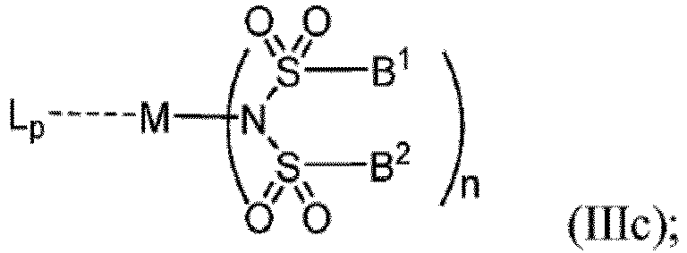
- the charge neutral metal amide compound of the hole injection layer may be selected from at least one compound according to Formula IIIa, IIIb, IIIc, IIId, IIIe, IIIf, IIIg, IIIh and/or IIIi, wherein for A 1 and A 2 are SO 2 :
- the charge neutral metal amide compound of the hole injection layer may be selected from at least one compound according to Formula IVa, IVb, IVc, IVd and/or IVe, wherein for A 1 and A 2 are POR 8 :
- the charge neutral metal amide compound of the hole injection layer may be selected from at least one compound according to Formula Va, Vb, Vc, Vd, Ve, Vf, Vg, Vh and/or Vi, wherein for A 1 and A 2 are CO:
- the charge neutral metal amide compound of the hole injection layer may be selected from at least one compound according to Formula VIa, wherein for A 1 is SO 2 and A 2 is POR 8 :
- charge neutral metal amide compound of the hole injection layer may be selected from at least one compound according to Formula Ib: wherein:
- the charge neutral metal amide compound of the hole injection layer may be selected from at least one compound according to Formula Id, wherein N, A 1 , B 1 , A 2 and B 2 form a first 5 to 10 member ring and B 1 and B 2 are bridged to form a second ring of a substituted or unsubstituted C 6 to C 20 aryl, or of a substituted or unsubstituted C 6 to C 20 heteroaryl ring:
- the charge neutral metal amide compound of the hole injection layer may be selected from at least one fluorinated compound according to:
- the charge neutral metal amide compound of the hole injection layer may be selected from at least one fluorinated compound, based on general formula Ia, having the Formula F1 to F23: wherein the charge neutral ligand L coordinates to the metal M: wherein
- Charge neutral metal amide compounds which contain a charge-neutral ligand L selected from mono and multidental ethers or amines forming a 5 to 7 membered ring system with the metal, preferably glycole ethers, ethylendiamine derivatives, even more preferred diglyme, and/or N1,N1,N2,N2-tetramethyl-1,2-ethanediamine, N-((E,2E)-2- ⁇ [(E)-1,1-dimethylethyl]imino ⁇ ethylidene)-2-methyl-2-propanamine can be preferably used as HIL-material.
- a charge-neutral ligand L selected from mono and multidental ethers or amines forming a 5 to 7 membered ring system with the metal, preferably glycole ethers, ethylendiamine derivatives, even more preferred diglyme, and/or N1,N1,N2,N2-tetramethyl-1,2-ethanediamine, N-((E,
- charge neutral metal amides compounds with a charge-neutral ligand L selected from mono and/or multidental ethers or amines that can be preferably used as HIL-material having the Formula F1, F2, F3, F4, F5 and/or F6: wherein
- the charge neutral metal amide compound of the hole injection layer may be selected preferably from at least one fluorinated compound, based on general formula Ia, having the Formula F18 to F23:
- the charge neutral metal amide compound of the hole injection layer may be selected preferably from at least one fluorinated compound, based on general formula Ia, having the Formula F24 to F45: wherein a halide, O, alkoxylate or amine bonds to the metal M: wherein
- Ligand G is selected from group VII elements, preferably chloride Cl.
- ligand G is selected from an alkoxylate of formula F30, F31 and F35: wherein
- the charge neutral metal amide compound of the hole injection layer may be selected preferably from at least one fluorinated compound, based on general formula Ia, having the Formula F36 to F46:
- HIL hole injection layer
- Table 1 Compounds of formula (Ia) which can be suitable used for an hole injection layer (HIL) Metal amide Structure CAS number Li TFSI 90076-65-6 Na TFSI 91742-21-1 K TFSI 90076-67-8 Cs TFSI 91742-16-4 Mg (TFSI) 2 133395-16-1 Fe (TFSI) 3 207861-59-4 Ag TFSI 189114-61-2 Mn (TFSI) 2 207861-55-0 Sn (TFSI) 4 1019840-51-7 Sm (TFSI) 3 222733-67-7 Lu (TFSI) 3 887919-24-6 Sc (TFSI) 3 176726-07-1 Nd (TFSI) 3 207861-67-4 U(O) 2 (TFSI) 2 943217-83-2 V(O) (TFSI) 3 --
- HIL hole injection layer
- the hole injection layer may comprises the charge neutral metal amide compound according to formula Ia, Ib, Ic and/or Id in the range of ⁇ 0.1 wt.-% to ⁇ 49 wt.-%, preferably ⁇ 0.5 wt.-% to ⁇ 45 wt.-%, further preferred ⁇ 1 wt.-% to ⁇ 40 wt.-%, in addition preferred ⁇ 1.5 wt.-% to ⁇ 30 wt.-%, or ⁇ 2 wt.-% to ⁇ 20 wt.-%, or ⁇ 2.5 wt.-% to ⁇ 10 wt.-%, or ⁇ 3 wt.-% to ⁇ 7 wt.-%, and more preferred ⁇ 3.5 wt.-% to ⁇ 5 wt.-% or ⁇ 4 wt.-% to ⁇ 4.5 wt.-%.
- HIL hole transport layer
- the hole injection layer comprises a triarylamine compound having the Formula VIIa: wherein:
- the substituent on Ar 1 is selected from phenyl, biphenyl, 2-(9,9-dialkyl-fluorenyl), 2-(9-alkyl-9'-aryl-fluorenyl) and 2-(9,9-diaryl-fluorenyl).
- the hole injection layer may comprises a triarylamine compound of Formula VIIa, wherein N, Ar 1 and Ar 3 form a carbazole ring;
- Ar 2 is phenyl or biphenyl;
- Ar 3 to Ar 6 are selected from phenyl, tolyl, xylyl, mesityl, biphenyl, 1-naphthyl, 2-napthyl, 2-(9,9-dialkyl-fluorenyl), 2-(9-alkyl-9'-aryl-fluorenyl) and 2-(9,9-diaryl-fluorenyl);
- R 9 single bond;
- the q may be selected from 1 or 2.
- Compounds of formula VIIa that can be suitable used as HIL-material may have an molecular weight suitable for thermal vacuum deposition and HOMO levels that provides a good hole injection performance into the emission layer.
- Compounds of formula VIIa that can be preferably used as HIL-material may have an molecular weight that is ⁇ 243 g/mol and ⁇ 2000 g/mol, even more preferred is ⁇ 412 g/mol and ⁇ 1800 g/mol, also preferred ⁇ 488 g/mol and ⁇ 1500 g/mol.
- the Ar 1 and Ar 2 of Formula VIIa may be independently selected from phenylene, biphenylene, naphthylene, anthranylene, carbazolylene, or fluorenylene, preferably from phenylene or biphenylene.
- the Ar 3 to Ar 6 of Formula VIIa may be independently selected from phenyl, biphenyl, terphenyl, quartphenyl, fluorenyl, napthyl, anthranyl, phenanthryl, thiophenyl, fluorenyl, or carbazolyl.
- Ar 3 to Ar 6 of Formula VIIa may be independently selected from phenyl, biphenyl, fluorenyl, napthyl, thiopheneyl, fluorenyl, or carbazolyl.
- At least two of Ar 1 to Ar 6 of Formula VIIa may form a cyclic structure, for example Ar 1 and Ar 3 ; or Ar 1 and Ar 4 ; or Ar 2 and Ar 5 ; or Ar 2 and Ar 6 ; may be a carbazole, phenazoline or phenoxazine ring.
- At least one of Ar 1 to Ar 6 of Formula VIIa may be unsubstituted, even more preferred at least two of Ar 1 to Ar 6 of Formula VII may be unsubstituted.
- the triarylamine compound has the Formula VIIb to VIIk.
- the hole injection layer may comprises a triarylamine compound of formula VIIa, wherein the substituents on Ar 3 to Ar 6 are independently selected from C 1 to C 12 alkyl, C 1 to C 12 alkoxy or halide, preferably from C 1 to C 8 alkyl or C 1 to C 8 heteroalkyl, even more preferred from C 1 to C 5 alkyl or C 1 to C 5 heteroalkyl.
- the hole injection layer comprises a triarylamine compound of formula VIIa, wherein the substituents on Ar 3 to Ar 6 are independently selected from C 1 to C 12 alkyl or halide, preferably from C 1 to C 8 alkyl or fluoride, even more preferred from C 1 to C 5 alkyl or fluoride.
- the HOMO level of the hole injection layer may have a HOMO level suitable for good hole injection into the emission layer, in particular of phosphorescent blue and green emitters and emission which relies on TADF (thermally activated delayed fluorescence) and the OLED may have low voltage, high efficiency and good stability.
- Triarylamine compounds of formula VIIa Name Structure HOMO (eV) N,N,N',N'-Tetrakis(4-methylphenyl)-benzidine (T-1) -4.99 N4,N4,N4',N4'-tetra(biphenyl-4-yl)biphenyl-4,4'-diamine (T-2) -5.08 Name Structure HOMO (eV) Biphenyl-4-yl(9,9-diphenyl-9H-fluoren-2-yl)-[4-(9-phenyl-9H-carbazol-3-yl)phenyl]-amine (T-3) -5.10 N,N'-Bis(naphthalen-1-yl)-N,N'-bis(phenyl)-benzidine (T-4) -5.11 N1,N3-di([1,1'-biphenyl]-4-yl)-5-(9,
- the hole injection layer may have a layer thickness of at least ⁇ 30 nm to ⁇ 1000 nm, preferably of ⁇ 40 nm to ⁇ 500 nm, also preferred of ⁇ 50 nm to ⁇ 750 nm.
- the hole injection layer may have a layer thickness of at least ⁇ 40 nm to ⁇ 1000 nm, preferably of ⁇ 60 nm to ⁇ 500 nm, also preferred of ⁇ 80 nm to ⁇ 750 nm.
- the hole injection layer may have a layer thickness of at least ⁇ 70 nm to ⁇ 1000 nm, preferably of ⁇ 90 nm to ⁇ 500 nm, also preferred of ⁇ 100 nm to ⁇ 600 nm.
- the hole injection layer may have a layer thickness of at least ⁇ 100 nm to ⁇ 1000 nm, preferably of ⁇ 150 nm to ⁇ 500 nm, also preferred of ⁇ 200 nm to ⁇ 450 nm.
- the hole injection layer may comprises:
- the hole injection layer may comprises:
- the hole injection layer may comprises:
- the hole injection layer may comprises:
- the hole injection layer may comprises the triarylamine compound according to Formula VIIa in the range of ⁇ 60 wt.-% to ⁇ 100 wt.-%, further preferred ⁇ 70 wt.-% to ⁇ 100 wt.-%, in addition preferred ⁇ 80 wt.-% to ⁇ 100 wt.-%, or ⁇ 95 wt.-% to ⁇ 100 wt.-%, or ⁇ 98 wt.-% to ⁇ 100 wt.-%, or ⁇ 99 wt.-% to ⁇ 100 wt.-%, and more preferred ⁇ 90 wt.-% to ⁇ 100 wt.-% or ⁇ 95 wt.-% to ⁇ 99 wt.-%.
- the hole injection layer may comprises the triarylamine compound according to Formula VIIa in the range of ⁇ 70 wt.-% to ⁇ 100 wt.-%, in addition preferred ⁇ 80 wt.-% to ⁇ 100 wt.-%, or ⁇ 95 wt.-% to ⁇ 100 wt.-%, or ⁇ 98 wt.-% to ⁇ 100 wt.-%, or ⁇ 99 wt.-% to ⁇ 100 wt.-%, and more preferred ⁇ 90 wt.-% to ⁇ 100 wt.-% or ⁇ 95 wt.-% to ⁇ 99 wt.-%.
- the hole injection layer may comprises the triarylamine compound according to Formula VIIa in the range of ⁇ 80 wt.-% to ⁇ 100 wt.-%, or ⁇ 95 wt.-% to ⁇ 100 wt.-%, or ⁇ 98 wt.-% to ⁇ 100 wt.-%, or ⁇ 99 wt.-% to ⁇ 100 wt.-%, and more preferred ⁇ 90 wt.-% to ⁇ 100 wt.-% or ⁇ 95 wt.-% to ⁇ 99 wt.-%.
- the hole injection layer may comprises the triarylamine compound according to Formula VIIa in the range of ⁇ 95 wt.-% to ⁇ 100 wt.-%, or ⁇ 98 wt.-% to ⁇ 100 wt.-%, or ⁇ 99 wt.-% to ⁇ 100 wt.-%, and more preferred ⁇ 90 wt.-% to ⁇ 100 wt.-% or ⁇ 95 wt.-% to ⁇ 99 wt.-%.
- the hole injection layer may comprises the triarylamine compound according to Formula VIIa in the range of ⁇ 98 wt.-% to ⁇ 100 wt.-%, or ⁇ 99 wt.-% to ⁇ 100 wt.-%, and more preferred ⁇ 90 wt.-% to ⁇ 100 wt.-% or ⁇ 95 wt.-% to ⁇ 99 wt.-%.
- the hole injection layer may comprises the triarylamine compound according to Formula VIIa in the range of ⁇ 99 wt.-% to ⁇ 100 wt.-%, and more preferred ⁇ 90 wt.-% to ⁇ 100 wt.-% or ⁇ 95 wt.-% to ⁇ 99 wt.-%.
- the hole injection layer comprises:
- HTL hole transport layer
- the HTL may be formed of any compound that is commonly used to form a HTL.
- Compound that can be suitably used is disclosed for example in Y. Shirota and H. Kageyama, Chem. Rev. 2007, 107, 953-1010 .
- Examples of the compound that may be used to form the HTL 140 are: a carbazole derivative, such as N-phenylcarbazole or polyvinylcarbazole; an amine derivative having an aromatic condensation ring, such as N,N'-bis(3-methylphenyl)-N,N'-diphenyl-[1,1-biphenyl]-4,4'-diamine (T-1), or N,N'-di(naphthalene-1-yl)-N,N'-diphenyl benzydine (alpha -NPD, T-4); and a triphenylamine-based compound, such as 4,4',4"-tris(N-carbazolyl)triphenylamine (T-10).
- HTL 140 Other examples of the compounds that may be used forming the HTL 140 are oligothiophenes and phthalocyanines disclosed for example in Yasuhiko Shirota and Hiroshi Kageyama, Chem. Rev. 2007, 107, 953-1010 and in Facchetti, MaterialsToday 10, 2007, 28.
- the OLED according to the present invention may not contain an electron transport layer (ETL). However, the OLED according to the present invention may optional contain an electron transport layer (ETL).
- ETL electron transport layer
- the OLED may comprises an electron transport layer or an electron transport layer stack comprising at least a first electron transport layer and at least a second electron transport layer.
- the electron transport layer may comprises at least one matrix compound.
- the thicknesses of the electron transport layer may be in the range of ⁇ 0.5 nm to ⁇ 95 nm, preferably of ⁇ 3 nm to ⁇ 80 nm, further preferred of ⁇ 5 nm to ⁇ 60 nm, also preferred of ⁇ 6 nm to ⁇ 40 nm, in addition preferred ⁇ 8 nm to ⁇ 20 nm and more preferred of ⁇ 10 nm to ⁇ 18 nm.
- the thicknesses of the electron transport layer stack can be in the range of ⁇ 25 nm to ⁇ 100 nm, preferably of ⁇ 30 nm to ⁇ 80 nm, further preferred of ⁇ 35 nm to ⁇ 60 nm, and more preferred of ⁇ 36 nm to ⁇ 40 nm.
- the electron transport layer comprises of ⁇ 50 wt.-% to ⁇ 60 wt.-% of a first lithium halide or a first lithium organic complex and ⁇ 50 wt.-% to ⁇ 40 wt.-% of a matrix compound of:
- the light-emitting diode may comprises at least two electrodes, an anode electrode and a second cathode electrode.
- the electron transport layer/s or electron transport layer stack is not an electrode.
- the electron transport layer/s or electron transport layer are sandwiched between two electrodes, namely sandwiched between an anode and a second cathode.
- the ETL may be formed optional on an EML or on the HBL if the HBL is formed.
- the ETL includes a first layer including a first lithium halide or a first lithium organic complex; and optional a second electron transport layer including a second lithium halide or a second lithium organic complex, wherein optional the first lithium organic complex is not the same as the second lithium organic complex and wherein the first lithium halide is not the same as the second lithium halide.
- the ETL includes a first layer comprising a first matrix compound and a lithium halide or a lithium organic complex; and optional a second electron transport layer comprising a second matrix compound and a metal dopant selected from a group comprising alkali, alkaline earth and rare earth metals.
- the ETL includes a first layer comprising a first matrix compound and a lithium halide or a lithium organic complex; and optional a second electron transport layer comprising a second matrix compound and is free of dopant.
- the ETL may have a stacked structure, preferably of two ETL-layers, so that injection and transport of electrons may be balanced and holes may be efficiently blocked.
- a conventional OLED since the amounts of electrons and holes vary with time, after driving is initiated, the number of excitons generated in an emission area may be reduced. As a result, a carrier balance may not be maintained, so as to reduce the lifetime of the OLED.
- the first layer and the second layer may have similar or identical energy levels, so that the carrier balance may be uniformly maintained, while controlling the electron-transfer rate.
- Matrix compound for the electron layer that can be suitable used are selected from the group comprising anthracene compounds, preferably 2-(4-(9,10-di(naphthalen-2-yl)anthracen-2-yl)phenyl)-1-phenyl-1H-benzo[d]imidazole
- Anthracene compounds that can be used as matrix materials are disclosed in US 6878469 B .
- diphenylphosphine oxide preferably (3-(dibenzo[c,h]acridin-7-yl)phenyl)diphenylphosphine oxide, phenylbis(3-(pyren-1-yl)phenyl)phosphine oxide, 3-phenyl-3H-benzo[b]dinaphtho[2,1-d:1',2'-f]phosphepine-3-oxide, phenyldi(pyren-1-yl)phosphine oxide.
- diphenylphosphine oxide preferably (3-(dibenzo[c,h]acridin-7-yl)phenyl)diphenylphosphine oxide, phenylbis(3-(pyren-1-yl)phenyl)phosphine oxide, 3-phenyl-3H-benzo[b]dinaphtho[2,1-d:1',2'-f]phosphepine-3-oxide, phenyl
- Diphenylphosphine oxide compounds that can be used as matrix materials are disclosed in EP 2395571 A1 , WO2013079217 A1 , EP 13187905 , EP13199361 and JP2002063989 A1 .
- Suitable matrix compounds that can be used are phenanthroline compounds, preferably selected from the group comprising of 2,4,7,9-tetraphenyl-1,10-phenanthroline, 4,7-diphenyl-2,9-di-p-tolyl-1,10-phenanthroline, and 2,9-di(biphenyl-4-yl)-4,7-diphenyl-1,10-phenanthroline.
- Phenanthroline compounds that can be used as matrix materials are disclosed in EP 1786050 A1 .
- the matrix compound of the electron transport layer may be a compound that efficiently transports electrons, such as an anthracene-based compound, diphenylphosphine oxide based compound, or a phenanthroline based compound, preferably a matrix compound mentioned in Table 4.
- the matrix compound of the electron transport layer may be selected from the group consisting of Compound 5, a compound represented by Formula 2, and a compound represented by Formula 3 below:
- R 1 to R 6 are each independently a hydrogen atom, a halogen atom, a hydroxy group, a cyano group, a substituted or unsubstituted C 1 -C 30 alkyl group, a substituted or unsubstituted C 1 -C 30 alkoxy group, a substituted or unsubstituted C 1 -C 30 acyl group, a substituted or unsubstituted C 2 -C 30 alkenyl group, a substituted or unsubstituted C 2 -C 30 alkynyl group, a substituted or unsubstituted C 6 -C 30 aryl group, or a substituted or unsubstituted C 3 -C 30 heteroaryl group.
- At least two adjacent R 1 to R 6 groups are optionally bonded to each other, to form a saturated or unsaturated ring.
- L 1 is a bond, a substituted or unsubstituted C 1 -C 30 alkylene group, a substituted or unsubstituted C 6 -C 30 arylene group, or a substituted or unsubstituted C 3 -C 30 hetero arylene group.
- Q 1 through Q 9 are each independently a hydrogen atom, a substituted or unsubstituted C 6 -C 30 aryl group, or a substituted or unsubstituted C 3 -C 30 hetero aryl group, and "a" is an integer from 1 to 10.
- R 1 to R 6 may be each independently selected from the group consisting of a hydrogen atom, a halogen atom, a hydroxy group, a cyano group, a methyl group, an ethyl group, a propyl group, a butyl group, a methoxy group, an ethoxy group, a propoxy group, a butoxy group, a phenyl group, a naphthyl group, an anthryl group, a pyridinyl group, and a pyrazinyl group.
- R 1 to R 4 may each be a hydrogen atom
- R 5 may be selected from the group consisting of a halogen atom, a hydroxy group, a cyano group, a methyl group, an ethyl group, a propyl group, a butyl group, a methoxy group, an ethoxy group, a propoxy group, a butoxy group, a phenyl group, a naphthyl group, an anthryl group, a pyridinyl group, and a pyrazinyl group.
- R 1 to R 6 may each be a hydrogen atom.
- Q 1 to Q 9 are each independently a hydrogen atom, a phenyl group, a naphthyl group, an anthryl group, a pyridinyl group, and a pyrazinyl group.
- Q 1 , Q 3 -Q 6 , Q 8 and Q 9 are hydrogen atoms
- Q 2 and Q 7 may be each independently selected from the group consisting of a phenyl group, a naphthyl group, an anthryl group, a pyridinyl group, and a pyrazinyl group.
- L 1 in Formula 2 and/or 3, may be selected from the group consisting of a phenylene group, a naphthylene group, an anthrylene group, a pyridinylene group, and a pyrazinylene group.
- L 1 may be a phenylene group or a pyridinylene group.
- "a" may be 1, 2, or, 3.
- the matrix compound for the ETL-layer may be further selected from Compound 5, 6, or 7 below: Table 4 Chemical structures of matrix materials that can be suitable used for ETL-layer Referred to as: IUPAC name Structure Reference MX 1 2-(4-(9,10-di(naphthalen-2-yl)anthracen-2-yl)phenyl)-1-phenyl-1H-benzo[d]imidazole US 6878469 B2 .
- the electron transport layer may comprises a lithium halide or a lithium organic complex.
- Suitable organic ligands to form a lithium organic complex that can be used for the electron transport layer are disclosed, for example in US 2014/0048792 and Kathirgamanathan, Poopathy; Arkley, Vincent; Surendrakumar, Sivagnanasundram; Chan, Yun F.; Ravichandran, Seenivasagam; Ganeshamurugan, Subramaniam; Kumaraverl, Muttulingam; Antipan-Lara, Juan; Paramaswara, Gnanamolly; Reddy, Vanga R., Digest of Technical Papers - Society for Information Display International Symposium (2010), 41(Bk. 1), 465-468 .
- Lithium organic complex that can be suitable used for the ETL-layer Refered to as: IUPAC name Structure Reference LiQ lithium 8-hydroxyquinolate WO 2013079217 A1 Li-1 lithium tetra(1H-pyrazol-1-yl)borate WO 2013079676 A1 Li-2 lithium 2-(diphenyl-phosphoryl)phenolate WO 2013079678A1 Li-3 lithium 2-(pyridin-2-yl)phenolate JP2 008195623 Li-4 lithium 2-(1-phenyl-1H-benzo[d]imidazol-2-yl)phenolate JP 2001291593 , Li-5 lithium 2-(benzo[d]oxazol-2-yl)phenolate US 20030165711 Li-6 lithium 2-(diphenyl-phosphoryl)pyridin-3-olate EP 2724388
- the organic ligand of the lithium organic complex of the electron transport layer may be selected from the group comprising a quinolate, a borate, a phenolate, a pyridinolate or a Schiff base ligand, or Table 5;
- the lithium halide of the electron transport layer may be selected from the group comprising a LiF, LiCl, LiBr or LiJ, and preferably LiF.
- the ETL may be formed on the EML by vacuum deposition, spin coating, slot-die coating, printing, casting, or the like.
- the deposition and coating conditions may be similar to those for formation of the HIL 130. However, the deposition and coating conditions may vary, according to a compound that is used to form the ETL.
- the substrate may be any substrate that is commonly used in manufacturing of organic light-emitting diodes. If light is emitted through the substrate, the substrate may be a transparent material, for example a glass substrate or a transparent plastic substrate, having excellent mechanical strength, thermal stability, transparency, surface smoothness, ease of handling, and waterproofness. If light is emitted through the top surface, the substrate may be a transparent or non-transparent material, for example a glass substrate, a plastic substrate, a metal substrate or a silicon substrate.
- the anode electrode may be formed by depositing or sputtering a compound that is used to form the anode electrode.
- the compound used to form the anode electrode may be a high work-function compound, so as to facilitate hole injection.
- the anode material may also be selected from a low work function material (i.e. Aluminum).
- the anode electrode may be a transparent or reflective electrode.
- Transparent conductive compounds such as indium tin oxide (ITO), indium zinc oxide (IZO), tin-dioxide (SnO 2 ), and zinc oxide (ZnO), may be used to form the anode electrode 120.
- the anode electrode 120 may also be formed using magnesium (Mg), aluminum (Al), aluminum-lithium (Al-Li), calcium (Ca), magnesium-indium (Mg-In), magnesium-silver (Mg-Ag), silver (Ag), gold (Au), or the like.
- the anode electrode may be formed from a high conductivity metal, for example copper (Cu) or silver (Ag).
- the HIL may be formed on the anode electrode by vacuum deposition, spin coating, printing, casting, slot-die coating, Langmuir-Blodgett (LB) deposition, or the like.
- the deposition conditions may vary according to the compound that is used to form the HIL, and the desired structure and thermal properties of the HIL. In general, however, conditions for vacuum deposition may include a deposition temperature of 100° C to 500° C, a pressure of 10 -8 to 10 -3 torr (1 torr equals 133.322 Pa), and a deposition rate of 0.1 to 10 nm/sec..
- coating conditions may vary according to a compound that is used to form the HIL, and the desired structure and thermal properties of the HIL.
- the coating conditions may include a coating speed of 2000 rpm to 5000 rpm, and a thermal treatment temperature of 80° C to 200° C. Thermal treatment removes a solvent after the coating is performed.
- the hole transport layer (HTL) may be formed on the HIL by vacuum deposition, spin coating, slot-die coating, printing, casting, Langmuir-Blodgett (LB) deposition, or the like.
- LB Langmuir-Blodgett
- the conditions for deposition and coating may be similar to those for the formation of the HIL.
- the conditions for the vacuum or solution deposition may vary, according to the compound that is used to form the HTL.
- Emission layer Emission layer
- the EML may be formed on the HTL by vacuum deposition, spin coating, slot-die coating, printing, casting, LB, or the like.
- the conditions for deposition and coating may be similar to those for the formation of the HIL. However, the conditions for deposition and coating may vary, according to the compound that is used to form the EML.
- the emission layer may be formed of a combination of a host and a dopant.
- Example of the host are Alq3, 4,4'-N,N'- dicarbazole-biphenyl (CBP), poly(n-vinylcarbazole) (PVK), 9,10-di(naphthalene-2-yl)anthracenee (ADN), 4,4',4"-Tris(carbazol-9-yl)-triphenylamine (TCTA), 1,3,5-tris(N-phenylbenzimidazole-2-yl)benzene (TPBI), 3-tert-butyl-9,10-di-2-naphthylanthracenee (TBADN), distyrylarylene (DSA), Bis(2-(2-hydroxyphenyl)benzo-thiazolate)zinc (Zn(BTZ) 2), E3 below, AND, Compound 1 below, and Compound 2 below. AND
- the dopant may be a phosphorescent or fluorescent emitter. Phosphorescent emitters are preferred due to their higher efficiency
- red dopant examples include PtOEP, Ir(piq) 3, and Btp 2lr(acac), but are not limited thereto. These compounds are phosphorescent emitters, however, fluorescent red dopants could also be used.
- Compound 3 is an example of a fluorescent green emitter and the structure is shown below.
- Examples of a phosphorescent blue dopant are F 2 Irpic, (F 2 ppy) 2 Ir(tmd) and Ir(dfppz) 3, ter-fluorene, the structures are shown below.
- 4.4'-bis(4-diphenyl amiostyryl)biphenyl (DPAVBi), 2,5,8,11-tetra-tert-butyl perylene (TBPe), and Compound 4 below are examples of fluorescent blue dopants.
- the amount of the dopant may be in the range of 0.01 to 50 parts by weight, based on 100 parts by weight of the host.
- the EML may have a thickness of 10 nm to 100 nm, for example, 20 nm to 60 nm. When the thickness of the EML is within this range, the EML may have excellent light emission, without a substantial increase in driving voltage.
- HBL Hole blocking layer
- a hole blocking layer may be formed on the EML, by using vacuum deposition, spin coating, slot-die coating, printing, casting, LB deposition, or the like, in order to prevent the diffusion of triplet excitons or holes into the ETL.
- the conditions for deposition and coating may be similar to those for the formation of the HIL. However, the conditions for deposition and coating may vary, according to the compound that is used to form the HBL. Any compound that is commonly used to form a HBL may be used. Examples of compounds for forming the HBL include an oxadiazole derivative, a triazole derivative, and a phenanthroline derivative.
- the HBL may have a thickness of 5 nm to 100 nm, for example, 10 nm to 30 nm. When the thickness of the HBL is within this range, the HBL may have excellent hole-blocking properties, without a substantial increase in driving voltage.
- Electron injection layer (EIL)
- the optional EIL which may facilitates injection of electrons from the cathode, may be formed on the ETL, preferably directly on the electron transport layer.
- materials for forming the EIL include LiF, NaCl, CsF, Li2O, BaO, Ca, Ba, Yb, Mg which are known in the art.
- Deposition and coating conditions for forming the EIL are similar to those for formation of the HIL, although the deposition and coating conditions may vary, according to a material that is used to form the EIL.
- the thickness of the EIL may be in the range of 0.1 nm to 10 nm, for example, in the range of 0.5 nm to 9 nm. When the thickness of the EIL is within this range, the EIL may have satisfactory electron-injecting properties, without a substantial increase in driving voltage.
- the cathode electrode is formed on the EIL if present.
- the cathode electrode may be a cathode, which is an electron-injecting electrode.
- the cathode electrode may be formed of a metal, an alloy, an electrically conductive compound, or a mixture thereof.
- the cathode electrode may have a low work function.
- the cathode electrode may be formed of lithium (Li), magnesium (Mg), aluminum (Al), aluminum (Al)-lithium (Li), calcium (Ca), barium (Ba), ytterbium (Yb), magnesium (Mg)-indium (In), magnesium (Mg)-silver (Ag), or the like.
- the cathode electrode may be formed of a transparent conductive material, such as ITO or IZO.
- the thickness of the cathode electrode may be in the range of 5 nm to 1000 nm, for example, in the range of 10 nm to 100 nm.
- the cathode electrode When the cathode electrode is in the range of 5 nm to 50 nm, the electrode will transparent even if a metal or metal alloy is used.
- the injection and transport of the electrons may be controlled, and the holes may be efficiently blocked.
- the OLED may have long lifetime.
- OLED Light-emitting diode
- an organic light-emitting diode comprising: a substrate; a anode electrode formed on the substrate; a hole injection layer comprising a metal amide according to the invention, a hole transport layer, an emission layer, and a cathode electrode.
- an organic light-emitting diode comprising: a substrate; a anode electrode formed on the substrate; a hole injection layer comprising a metal amide according to the invention, a hole transport layer, an emission layer, hole blocking layer and a cathode electrode.
- an organic light-emitting diode comprising: a substrate; a anode electrode formed on the substrate; a hole injection layer comprising a charge neutral metal amide according to the invention, a hole transport layer, an emission layer, hole blocking layer, electron transport layer, and a cathode electrode.
- an organic light-emitting diode comprising: a substrate; a anode electrode formed on the substrate; a hole injection layer comprising a charge neutral metal amide according to the invention, a hole transport layer, an emission layer, hole blocking layer, electron transport layer, an electron injection layer, and a cathode electrode.
- an organic light-emitting diode comprising: at least one layer selected from the group consisting of a hole injection layer, a hole transport layer, an emission layer, a hole blocking layer, an electron transport layer, exactly in that order between the anode electrode and the cathode electrode.
- an organic light-emitting diode further comprising an electron injection layer formed between the electron transport layer and the cathode electrode.
- the OLED may not comprises an electron injection layer.
- the OLED may not comprises an electron transport layer.
- the OLED may not comprises an electron transport layer and an electron injection layer.
- OLED organic light-emitting diode
- the method may further include forming on the anode electrode an hole injection layer, an hole transport layer, an emission layer and a cathode electrode, exactly in that order.
- the method may further include forming on the anode electrode an hole injection layer, an hole transport layer, an emission layer, an electron transport layer, and a cathode electrode, exactly in that order.
- the method may further include forming on the anode electrode an hole injection layer, an hole transport layer, hole blocking layer, an emission layer, an electron transport layer, and a cathode electrode, exactly in that order.
- the method may further include the steps for forming an organic light-emitting diode (OLED), wherein
- the method of manufacturing the OLED may comprise the steps:
- the layers are deposited the other way around, starting with the cathode, and sandwiched between the cathode and the anode.
- the anode electrode and/or the cathode electrode can be deposit on a substrate.
- the anode is deposit on a substrate.
- first element when a first element is referred to as being formed or disposed "on" a second element, the first element can be disposed directly on the second element, or one or more other elements may be disposed there between.
- first element when referred to as being formed or disposed "directly on” a second element, no other elements are disposed there between.
- FIG. 1 is a schematic sectional view of an organic light-emitting diode (OLED) 100, according to an exemplary embodiment of the present invention.
- the OLED 100 includes a substrate 110. On the substrate 110 an anode 120 is disposed. On the anode 120 a hole injection layer 130 containing or consisting of a metal amide compound according to the invention is disposed and thereon a hole transport layer 140. Onto the hole transport layer 140 an emission layer 150 and an cathode electrode 190, exactly in this order, are disposed.
- FIG. 2 is a schematic sectional view of an organic light-emitting diode (OLED) 100, according to an exemplary embodiment of the present invention.
- the OLED 100 includes a substrate 110, a first electrode 120, a hole injection layer (HIL) 130, a hole transport layer (HTL) 140, an emission layer (EML) 150, an electron transport layer (ETL) 161.
- the electron transport layer (ETL) 161 is formed directly on the EML 150.
- a cathode electrode 190 is disposed onto the electron transport layer (ETL) 161 .
- ETL electron transport layer stack
- Fig. 3 is a schematic sectional view of an OLED 100, according to another exemplary embodiment of the present invention.
- Fig. 3 differs from Fig. 2 in that the OLED 100 of Fig. 3 comprises a hole blocking layer (HBL) 155 and an electron injection layer (ElL) 180.
- HBL hole blocking layer
- ElL electron injection layer
- the OLED 100 includes a substrate 110, an anode electrode 120, a hole injection layer (HIL) 130, a hole transport layer (HTL) 140, an emission layer (EML) 150, a hole blocking layer (HBL) 155, an electron transport layer (ETL) 161, an electron injection layer (EIL) 180 and a cathode electrode 190.
- the layers are disposed exactly in the order as mentioned before.
- an OLED of the present invention is started with a substrate 110 onto which an anode electrode 120 is formed, on the anode electrode 120, an hole injection layer 130, hole transport layer 140, an emission layer 150, optional a hole blocking layer 155, optional at least one electron transport layer 161, optional at least one electron injection layer 180, and a cathode electrode 190 are formed, exactly in that order or exactly the other way around.
- a sealing layer may further be formed on the cathode electrodes 190, in order to seal the OLEDs 100.
- various other modifications may be applied thereto.
- a 15 ⁇ /cm 2 glass substrate available from Corning Co.
- 100 nm ITO was cut to a size of 50 mm x 50 mm x 0.7 mm, ultrasonically washed with isopropyl alcohol for 5 minutes and then with pure water for 5 minutes, and washed again with UV ozone for 30 minutes, to prepare a first electrode.
- the anode electrode was formed from 100 nm silver on glass which was prepared by the same methods as described above.
- the hole injection layer, triarylamine compound and a charge neutral metal amide compound according to the examples of Table 6 was vacuum co-deposited on the ITO electrode, to form a HIL having a thickness according to the examples 1 to 22 and comparative examples 1 to 5 of tables 6, 7 and 8.
- the corresponding hole injection layer according to the examples 1 to 22 and comparative examples 1 to 5 of tables 6, 7 and 8 was vacuum deposited on the HIL, to form a HTL having a thickness as mentioned in tables 6, 7 and 8, respectively.
- the wt.-% of the HIL-compound/s and HTL-compound according to the examples 1 to 22 and comparative examples 1 to 5 can be taken from Tables 6, 7 and 8 below, whereby the wt.-% amount of the HIL-compound/s is 100 wt.-% based on the total weight amount of the HIL-layer, and the wt.-% amount of the HTL-compound/s is 100 wt.-% based on the total weight amount of the HTL-layer, if no not indicated otherwise the wt.-% of the components are indicated in Tables 6, 7 and 8, respectively. That means that the HIL according to examples 1 to 22 consist of the triarylamine compound and metal amide compound according to the invention. However, the hole injection layer may comprises traces of the compound of the hole transport layer, due to the process of manufacture.
- the ETL-layer of matrix compound of 50 wt.-% MX 2 and 50 wt.-% LiQ (50 wt.-% : 50 wt.-%) having a thickness of 36 nm is formed by deposing the matrix compound from a first deposition source and the lithium organic complex or lithium halide from a second deposition source directly on the EML.
- the cathode was evaporated at ultra-high vacuum of 10 -7 bar. Therefore, a thermal single co-evaporation of one or several metals was performed with a rate of 0, 1 to 10 nm/s (0,01 to 1 ⁇ /s) in order to generate a homogeneous cathode with a thickness of 5 to 1000 nm.
- the cathode electrode was formed from 13 nm magnesium (90 vol.-%)-silver (10 vol.-%) alloy.
- the cathode electrode was formed from 100 nm aluminum.
- the OLED stack is protected from ambient conditions by encapsulation of the device with a glass slide. Thereby, a cavity is formed, which includes a getter material for further protection.
- the current efficiency is measured under ambient conditions (20°C). Current voltage measurements are performed using a Keithley 2400 sourcemeter, and recorded in V. At 10 mA/cm 2 for bottom emission and 15 mA/cm 2 for top emission devices, a calibrated spectrometer CAS140 from Instrument Systems is used for measurement of CIE coordinates and brightness in Candela. Lifetime LT of the device is measured at ambient conditions (20°C) and 15 mA/cm 2 , using a Keithley 2400 sourcemeter, and recorded in hours. The brightness of the device is measured using a calibrated photo diode. The lifetime LT is defined as the time till the brightness of the device is reduced to 97 % of its initial value.
- the emission is predominately Lambertian and quantified in percent external quantum efficiency (EQE).
- EQE percent external quantum efficiency
- the efficiency EQE will be higher compared to bottom emission devices.
- the light output of the device is measured using a calibrated photodiode at 15 mA/cm 2 .
- HIL very thick hole injection layers
- Example 1 T-3 Li(TFSI) 2 100 T-3 30 4.7
- Example 2 T-3 Li(TFSI) 2 150 T-3 30 4.8
- Example 3 T-3 Li(TFSI) 2 200 T-3 30 4.9
- Example 4 T-3 Li(TFSI) 2 250 T-3 30 5
- Example 5 T-3 Li(TFSI) 2 300 T-3 30 5
- Example 6 T-3 Li(TFSI) 2 350 T-3 30 5.1
- Example 8 T-3 Li(TFSI) 2 450 T-3 30 5.3
- Table 7 is shown the effect of the HIL and HTL thickness on performance of bottom emission devices.
- the thickness of the layers is selected in such a way that the sum of the thickness of HIL and HTL is kept constant at 130 nm. Thereby, the cavity does not change and light outcoupling and efficiency EQE are not impacted.
- the compound CNHAT (CAS 105598-27-4) has been used as a hole injection layer.
- a 10 nm layer of CNHAT was used.
- the efficiency EQE of 4.9 % was obtained at a voltage of 5.4 V.
- the efficiency EQE of 4.2 % was achieved at 4.7 V.
- the efficiency EQE is reduced at thicknesses which would level out non-uniformities.
- Example 9 to 15 shows the effect of increased thickness of the HIL comprising triarylamine T-3 and metal amide Li(TFSI) on efficiency, voltage and voltage stability over time.
- the efficiency is always higher than the efficiency obtained for devices containing a CNHAT HIL layer.
- the efficiency EQE remains constant for a HIL thickness ranging from 20 to 120 nm.
- the voltage for a 20 nm HIL layer is slightly higher compared to the comparative examples but surprisingly, the voltage decreases to 4.8 to 4.9 V for thicker layers (example 10 to 15).
- the voltage stability of all examples is at an acceptable level, for example less than 0.35V over 50 hours stability test at 15 mA/cm 2 .
- Example 16 to 20 triarylamine T-3 doped with Li(TFSI), Ag(TFSI), Mg(TFSI) 2 , Mn(TFSI) 2 and Li(cTFSI) (CAS 189217-62-7).
- the efficiency EQE is always higher than for comparative example 3 with CNHAT. Particularly high efficiency is obtained for a Ag(TFSI) doped HIL (example 18), while the lowest voltage and least voltage increase over time is achieved for Mg(TFSI) and Mn(TFSI) 2 (example 17 and 19, respectively).
- HTL for example band-gap or triplet level
- HTL materials of different OLEDs may differ in their HOMO level. Consequently, a good hole injection layer enables hole injection in to a large variety of HTL materials.
- HTLs which show low performance with the fluorescent blue EML used here may show unique performance with a different EML composition, for example phosphorescent blue or green EML, or for TADF (thermally activated delayed fluorescence) emitters.
- the hole injection performance is evaluated relative to CNHAT which is not suitable for injection into deep HOMO HTLs.
- CNHAT HIL is used together with deeper HOMO triarylamine compound T-8 (HOMO -5.25 eV) and T-9 (HOMO -5.33 eV).
- both open-chain and cyclic amide ligands show the desired effect (Li(TFSI) compared to Li(cTFSI), example 16 and 20, respectively).
- the invention is particularly useful for efficient hole injection into deeper HOMO HTLs which are required for OLEDs which rely on phosphorescent or TADF emitters, in particular green and blue emitters.
- OLED organic light-emitting diode
- EML emission layer
- An organic light-emitting diode (OLED) comprising more than one emission layer is also described as a tandem OLED or stacked OLED.
- OLED organic light-emitting diode
- a device comprising organic light-emitting diodes (OLED) is for example a display or a lighting panel.
Landscapes
- Chemical & Material Sciences (AREA)
- Physics & Mathematics (AREA)
- Engineering & Computer Science (AREA)
- Materials Engineering (AREA)
- Optics & Photonics (AREA)
- Spectroscopy & Molecular Physics (AREA)
- Inorganic Chemistry (AREA)
- Electroluminescent Light Sources (AREA)
Claims (20)
- Lochinjektionsschicht für eine OLED, umfassend eine Triarylaminverbindung, die mit einer ladungsneutralen Metallamidverbindung (Ia) dotiert ist, dadurch gekennzeichnet, dass die Lochinjektionsschicht eine Dicke von wenigstens ≥ 20 nm bis ≤ 1000 nm aufweist und die ladungsneutrale Metallamidverbindung die Formel Ia aufweist:
 G = Halogenid, O, Alkoxylat oder Amin der Formel IIa bis IIe:
 R1 bis R5 unabhängig ausgewählt sind aus der Gruppe umfassend H, C1- bis C20-Alkyl, C1- bis C20-Heteroalkyl, unsubstituiertes oder C1- bis C12-substituiertes C6- bis C20-Aryl, unsubstituiertes oder C1- bis C12-substituiertes Heteroaryl mit 5 bis 20 ringbildenden Atomen, halogeniertes oder perhalogeniertes C1- bis C20-Alkyl, halogeniertes oder perhalogeniertes C1- bis C20-Heteroalkyl, halogeniertes oder perhalogeniertes C6- bis C20-Aryl, halogeniertes oder perhalogeniertes Heteroaryl mit 5 bis 20 ringbildenden Atomen; oder
wenigstens ein R1 und R4 und/oder R2 und R3 und/oder R1 und R5 verbrückt ist und einen 5-bis 20-gliedrigen Ring bildet;m = 0, 1, 2, 3 oder 4;M = ein Metall ausgewählt aus der Gruppe umfassend Alkalimetall, Erdalkalimetall, Al, Ga, In, Übergangsmetall und Seltenerdmetall;
wobei die Bindung zwischen N und dem Metall M eine kovalente Bindung ist oder N eine nichtkovalente Wechselwirkung mit dem Metall M bildet;L = ladungeneutraler Ligand, der an das Metall M koordiniert, ausgewählt aus der Gruppe umfassend H2O, C2- bis C40-ein- oder mehrzähnige Ether und C2- bis C40-Thioether, C2- bis C40-Amine, C2- bis C40-Phosphine, C2- bis C20-Alkylnitril und C2- bis C40-Arylnitril, oder eine Verbindung gemäß Formel (III):
wenigstens ein R6 und R7 verbrückt ist und einen 5- bis 20-gliedrigen Ring bildet, oder die beiden R6 und/oder die beiden R7 verbrückt sind und einen 5- bis 40-gliedrigen Ring bilden oder einen 5- bis 40-gliedrigen Ring bilden, der ein unsubstituiertes oder C1- bis C12-substituiertes Phenanthrolin umfasst;p = 0, 1, 2 oder 3;A1, A2, A3 und A4 unabhängig ausgewählt sind aus CO, SO2 und POR8;R8 = elektronenziehende Gruppe ausgewählt aus der Gruppe umfassend Halogenid, Nitril, halogeniertes oder perhalogeniertes C1- bis C20-Alkyl, halogeniertes oder perhalogeniertes C6- bis C20-Aryl und halogeniertes oder perhalogeniertes Heteroaryl mit 5 bis 20 ringbildenden Atomen;n = 1, 2, 3, 4 oder 5;B1, B2, B3 und B4 gleich oder unabhängig ausgewählt sind aus substituiertem oder unsubstituiertem C1- bis C20-Alkyl, substituiertem oder unsubstituiertem C1- bis C20-Heteroalkyl, substituiertem oder unsubstituiertem C6- bis C20-Aryl, substituiertem oder unsubstituiertem C5- bis C20-Heteroaryl, oder B1 und B2 verbrückt sind;wobei, wenn B1 und B2 verbrückt sind:- M, N, A1, B1, B2, A2 und N bilden einen 7- bis 10-gliedrigen Ring gemäß Formel Ib,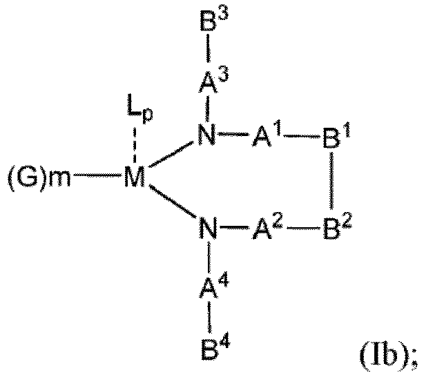 - N, A1, B1, B2 und A2 bilden einen 5- bis 10-gliedrigen Ring gemäß Formel Ic;
 - N, A1, B1, B2 und A2 bilden einen ersten, 5- bis 10-gliedrigen Ring und B1 und B2 bilden einen zweiten, 5- bis 20-gliedrigen Ring, gemäß Formel Id;wobei die Lochinjektionsschicht frei von einer Triarylverbindung gemäß: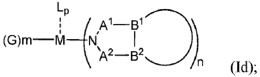

- Lochinjektionsschicht gemäß Anspruch 1,
wobei die Triarylaminverbindung die Formel Vlla aufweist: Ar1 und Ar2 = unabhängig ausgewählt aus substituiertem oder unsubstituiertem C6-bis C20-Arylen;Ar3 und Ar4 = unabhängig ausgewählt aus substituiertem oder unsubstituiertem C6-bis C20-Aryl;Ar5 und Ar6 = unabhängig ausgewählt aus substituiertem oder unsubstituiertem C6-bis C20-Aryl oder C5- bis C40-Heteroaryl;R9 = eine chemische Einfachbindung, ein unsubstituiertes oder substituiertes C1-bis C6-Alkyl oder ein unsubstituiertes oder substituiertes C1- bis C8-Heteroalkyl;q = 0, 1 oder 2;r = 0 oder 1;wobei- die Substituenten Ar1 bis Ar6 unabhängig ausgewählt sind aus C1- bis C20-Alkyl, C1- bis C20-Heteroalkyl und Halogen; und- die Substituenten für R9 unabhängig ausgewählt sind aus C1- bis C6-Alkyl, C1- bis C5-Heteroalkyl, C6- bis C20-Aryl und C5- bis C20-Heteroaryl;wobei die ladungsneutrale Metallamidverbindung die Formel Ia, Ib, Ic oder Id aufweist.
 - Lochinjektionsschicht gemäß Anspruch 1 oder 2, wobei die ladungsneutrale Metallamidverbindung die Formel Ia aufweist,
 A1 und A2 gleich oder unabhängig ausgewählt sind aus CO, POR8 und SO2, wobei A1 und A2 vorzugsweise gleich ausgewählt sind aus CO, POR8, SO2; oderA1 und A2 unabhängig ausgewählt sind aus CO, POR8, SO2, undN, A1, B1, A2 und B2 einen 5- bis 10-gliedrigen Ring bilden.
 - Lochinjektionsschicht gemäß einem der Ansprüche 1 bis 3,
wobei für:- p = 0, m = 1, 2, 3 oder 4, und n = 1, 2, 3 oder 4: die ladungsneutrale Metallamidverbindung weist die Formel IIa auf: - p = 1, 2 oder 3, und n = 1, 2, 3 oder 4, und m = 0: die ladungsneutrale Metallamidverbindung weist die Formel IIb auf:
 - p = 1, 2 oder 3, n = 1, 2, 3 oder 4, m = 1, 2, 3 oder 4, und N, A1, B1, B2 und A2 bilden einen 5-bis 10-gliedrigen Ring: die ladungsneutrale Metallamidverbindung weist Formel IIc auf:
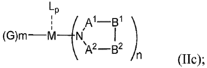 - p = 1, 2 oder 3, n= 1, 2, 3 oder 4, m = 1, 2, 3 oder 4, und N, A1, B1, B2 und A2 bilden einen ersten, 5- bis 10-gliedrigen Ring und B1 und B2 sind verbrückt, um einen zweiten, 5- bis 20-gliedrigen Ring zu bilden: die ladungsneutrale Metallamidverbindung weist die Formel IId auf:
 - p = 1, 2 oder 3, n = 1, m = 1, 2, 3 oder 4, und M, N, A1, B1, B2 und A2 und N bilden einen 7- bis 10-gliedrigen Ring: die ladungsneutrale Metallamidverbindung weist die Formel IIe auf:
 - p = 1, 2 oder 3, n = 1, 2, 3 oder 4, m = 0, und N, A1, B1, B2 und A2 bilden einen 5- bis 10-gliedrigen Ring: die ladungsneutrale Metallamidverbindung weist die Formel IIf auf:
 - p = 1, 2 oder 3, n = 1, 2, 3 oder 4, m = 0, und N, A1, B1, B2 und A2 bilden einen ersten, 5- bis 10-gliedrigen Ring und B1 und B2 sind verbrückt, um einen zweiten, 5- bis 20-gliedrigen Ring zu bilden: die ladungsneutrale Metallamidverbindung weist die Formel IIg auf:
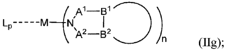 - p = 1, 2 oder 3, n = 1, m = 0, und M, N, A1, B1, B2 und A2 und N bilden einen 7- bis 10-gliedrigen Ring: die ladungsneutrale Metallamidverbindung weist die Formel IIh auf:
- Lochinjektionsschicht gemäß einem der Ansprüche 1 bis 4,
wobei, wenn A1 und A2 SO2 sind:- p = 1, 2 oder 3, n = 1, 2, 3 oder 4, m = 1, 2, 3 oder 4: die ladungsneutrale Metallamidverbindung weist die Formel IIIa auf: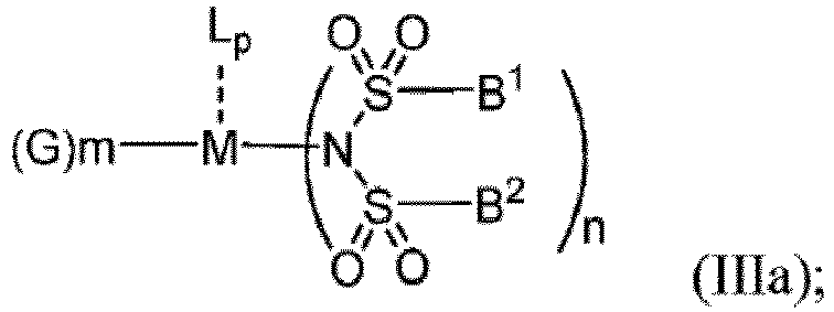 - p = 0, n = 1, 2, 3 oder 4, m = 1, 2, 3 oder 4: die ladungsneutrale Metallamidverbindung weist die Formel IIIb auf:
 - p = 1, 2 oder 3, n = 1, 2, 3 oder 4, m = 0, die ladungsneutrale Metallamidverbindung weist die Formel IIIc auf:
 - p = 1, 2 oder 3, n = 1, 2, 3 oder 4, m = 1, 2, 3 oder 4, und N, SO2, B1, B2 und SO2 bilden einen 5-bis 10-gliedrigen Ring: die ladungsneutrale Metallamidverbindung weist die Formel IIId auf:
 - p = 1, 2 oder 3, n = 1, 2, 3 oder 4, m = 1, 2, 3 oder 4, und N, SO2, B1, B2 und SO2 bilden einen ersten, 5- bis 10-gliedrigen Ring und B1 und B2 sind verbrückt und bilden einen zweiten, 5- bis 20-gliedrigen Ring: die ladungsneutrale Metallamidverbindung weist die Formel IIIe auf:
 - p = 1, 2 oder 3, n = 1, m = 1, 2, 3 oder 4, und M, N, SO2, B1, B2 und SO2 und N bilden einen 7-bis 10-gliedrigen Ring: die ladungsneutrale Metallamidverbindung weist die Formel IIIf auf:
 - p = 1, 2 oder 3, n = 1, 2, 3 oder 4, m = 0, und N, SO2, B1, B2 und SO2 bilden einen 5- bis 10-gliedrigen Ring: die ladungsneutrale Metallamidverbindung weist die Formel IIIg auf:
 - p = 1, 2 oder 3, n = 1, 2, 3 oder 4, m = 0, und N, SO2, B1, B2 und SO2 bilden einen ersten, 5- bis 10-gliedrigen Ring und B1 und B2 sind verbrückt und bilden einen zweiten, 5- bis 20-gliedrigen Ring: die ladungsneutrale Metallamidverbindung weist die Formel IIIh auf:
 - p = 1, 2 oder 3, n = 1, 2, 3 oder 4, m = 0, und M, N, SO2, B1, B2 und SO2 und N bilden einen 7-bis 10-gliedrigen Ring: die ladungsneutrale Metallamidverbindung weist die Formel IIIi auf:wobei, wenn A1 und A2 POR8 sind:
 - p = 1, 2 oder 3, m = 1, 2, 3 oder 4, und n = 1, 2, 3 oder 4: die ladungsneutrale Metallamidverbindung weist die Formel IVa auf:
 - p = 0, m = 1, 2, 3 oder 4, und n = 1, 2, 3 oder 4: die ladungsneutrale Metallamidverbindung weist die Formel IVb auf:
 - p = 1, 2 oder 3, m = 0, und n = 1, 2, 3 oder 4: die ladungsneutrale Metallamidverbindung weist die Formel IVc auf:
 - p = 1, 2 oder 3, n = 1, 2, 3 oder 4, m = 1, 2, 3 oder 4, und N, POR8, B1, B2 und POR8 bilden einen 5- bis 10-gliedrigen Ring: die ladungsneutrale Metallamidverbindung weist die Formel (IVd) auf:
 - p = 1, 2 oder 3, n = 1, 2, 3 oder 4, m = 0, und N, POR8, B1, B2 und POR8 bilden einen 5- bis 10-gliedrigen Ring: die ladungsneutrale Metallamidverbindung weist die Formel (IVe) auf:wobei, wenn A1 und A2 CO sind:
 - p = 1, 2 oder 3, m = 1, 2, 3 oder 4, und n = 1, 2, 3 oder 4: die ladungsneutrale Metallamidverbindung weist die Formel Va auf:
 - p = 0, n = 1, 2, 3 oder 4, m = 1, 2, 3 oder 4: die ladungsneutrale Metallamidverbindung weist die Formel Vb auf:
 - p = 1, 2 oder 3, n = 1, 2, 3 oder 4, m = 0: die ladungsneutrale Metallamidverbindung weist die Formel Vc auf:
 - p= 1, 2 oder 3, n = 1, 2, 3 oder 4, m = 1, 2, 3 oder 4, und N, CO, B1, B2 und CO bilden einen 5-bis 10-gliedrigen Ring: die ladungsneutrale Metallamidverbindung weist die Formel Vd auf:
 - p= 1, 2 oder 3, n = 1, 2, 3 oder 4, m = 1, 2, 3 oder 4, und N, CO, B1, B2 und CO bilden einen ersten, 5- bis 10-gliedrigen Ring und B1 und B2 sind verbrückt und bilden einen zweiten, 5- bis 20-gliedrigen Ring: die ladungsneutrale Metallamidverbindung weist die Formel Ve auf:
 - p = 1, 2 oder 3, n = 1, m = 1, 2, 3 oder 4, und M, N, CO, B1, B2, CO und N bilden einen 7- bis 10-gliedrigen Ring: die ladungsneutrale Metallamidverbindung weist die Formel Vf auf:
 - p = 1, 2 oder 3, n = 1, 2, 3 oder 4, m = 0, und N, CO, B1, B2 und CO bilden einen 5- bis 10-gliedrigen Ring: die ladungsneutrale Metallamidverbindung weist die Formel (Vg) auf:
 - p = 1, 2 oder 3, n = 1, 2, 3 oder 4, m = 0, und N, CO, B1, B2 und CO bilden einen ersten, 5- bis 10-gliedrigen Ring und B1 und B2 bilden einen zweiten, 5- bis 20-gliedrigen Ring: die ladungsneutrale Metallamidverbindung weist die Formel Vh auf:
 - p = 1, 2 oder 3, n = 1, 2, 3 oder 4, m = 0, und M, N, CO, B1, B2, CO und N bilden einen 7- bis 10-gliedrigen Ring: die ladungsneutrale Metallamidverbindung weist die Formel (Vi) auf:wobei, wenn A1 SO2 ist und A2 POR8 ist:
 - p = 1, 2 oder 3, m = 1, 2, 3 oder 4, und n = 1, 2, 3 oder 4: die ladungsneutrale Metallamidverbindung weist die Formel VIa auf:
- Lochinjektionsschicht gemäß einem der Ansprüche 1 bis 5, wobei
B1, B2, B3 und B4 unabhängig ausgewählt sind aus einem substituierten C1- bis C20-Alkyl, substituierten C1-bis C20-Heteroalkyl, substituierten C6- bis C20-Aryl oder substituierten C5- bis C20-Heteroaryl;
wobei
der Substituent eine elektronenziehende Gruppe ausgewählt aus der Gruppe umfassend ein Halogenid, Nitril, perhalogeniertes C1- bis C20-Alkyl, perhalogeniertes C6- bis C20-Aryl, perhalogeniertes Heteroaryl mit 6 bis 20 ringbildenden Atomen ist, wobei die elektronenziehende Gruppe vorzugsweise ein Fluorid, perfluoriertes C1- bis C20-Alkyl, perfluoriertes C6- bis C20-Aryl oder perfluoriertes Heteroaryl mit 5 bis 20 ringbildenden Atomen ist. - Lochinjektionsschicht gemäß einem der Ansprüche 1 bis 6, wobei m = 0, 1 oder 2.
- Lochinjektionsschicht gemäß einem der Ansprüche 1 bis 7, wobei M ausgewählt ist aus Li(I), Na(I), K(I), Cs(I), Mg(II), Ca(II), Sr(II), Ba(II), Sc(III), Y(III), Ti(IV), V(III-V), Cr(III-VI), Mn(II), Mn(III), Fe(II), Fe(III), Co(II), Co(III), Ni(II), Cu(I), Cu(II), Zn(II), Ag(I), Au(I), Au(III), Al(III), Ga(III), In(III), Sn(II), Sn(IV) und Pb(II); wobei M vorzugsweise ausgewählt ist aus Li(I), Mg(II), Mn(II) und Ag(I); und M bevorzugter ausgewählt ist aus Mg(II) und Li(I).
- Lochinjektionsschicht gemäß einem der Ansprüche 1 bis 8, wobei die ladungsneutrale Metallamidverbindung die Formel Ib aufweist:
 A3 und A4 gleich oder unabhängig ausgewählt sind aus CO, POR8 und SO2, wobei A3 und A4 vorzugsweise gleich ausgewählt sind aus CO, POR8 und SO2;B3 und B4 unabhängig ausgewählt sind aus substituiertem oder unsubstituiertem C1-bis C20-Alkyl, substituiertem oder unsubstituiertem C1- bis C20-Heteroalkyl, substituiertem oder unsubstituiertem C6-bis C20-Aryl, substituiertem oder unsubstituiertem C6- bis C20-Heteroaryl, wobei B3 und B4 vorzugsweise gleich ausgewählt sind; undM, N, A1, B1, A2 und B2 einen 7- bis 10-gliedrigen Ring bilden.
 - Lochinjektionsschicht gemäß einem der Ansprüche 1 bis 9, wobei N, A1, B1, A2 und B2 einen ersten, 5-bis 10-gliedrigen Ring bilden und B1 und B2 gemäß Formel Id:

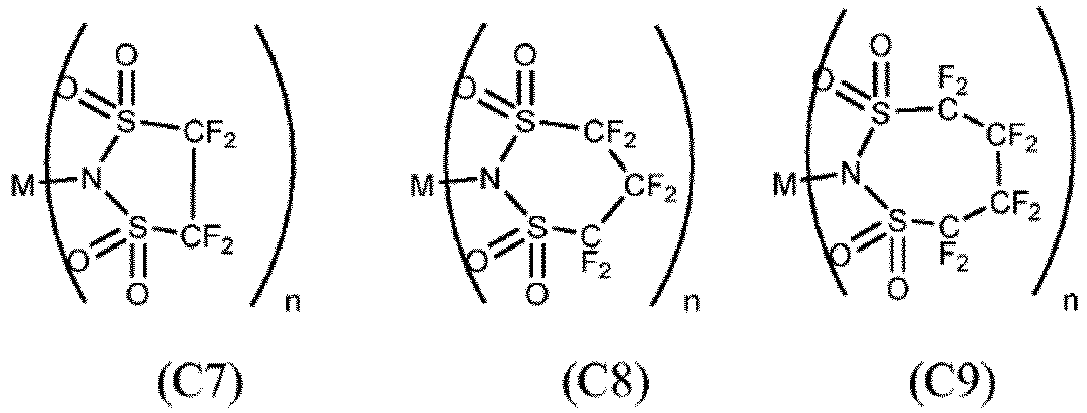
- Lochinjektionsschicht gemäß einem der Ansprüche 1 bis 10, wobei die ladungsneutrale Metallamidverbindung ausgewählt ist aus wenigstens einer der fluorierten Verbindungen gemäß Formel C1 bis C25:
wobei- Formel C1 bis C16, wobei p = 0, m = 0, n = 1, 2, 3 oder 4, und A1 und A2 SO2 sind:



 - Formel C17 bis C23, wobei n = 1, 2, 3 oder 4, und A1 und A2 CO sind:

 - Formel C24 bis C25, wobei n = 1, 2, 3 oder 4, A1 und A2 POR8 sind:
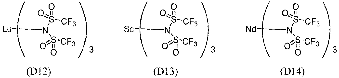
- Lochinjektionsschicht gemäß einem der Ansprüche 1 bis 11, wobei die ladungsneutrale Metallamidverbindung ausgewählt ist aus wenigstens einer fluorierten Verbindung gemäß Formel D1 bis D24:
wobei p = 0, m = 0, n = 1, 2, 3 oder 4, und A1 und A2 SO2 sind:




- Lochinjektionsschicht gemäß einem der Ansprüche 1 bis 12, wobei die ladungsneutrale Metallamidverbindung ausgewählt ist aus wenigstens einer fluorierten Verbindung gemäß Formel F1 bis F23:
wobei der ladungsneutrale Ligand L an das Metall M koordiniert:
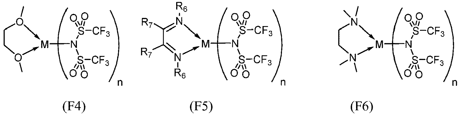


 R6 und R7 unabhängig ausgewählt sind aus C1- bis C20-Alkyl, C1- bis C20-Heteroalkyl, C6- bis C20-Aryl, Heteroaryl mit 5 bis 20 ringbildenden Atomen, halogeniertem oder perhalogeniertem C1- bis C20-Alkyl, halogeniertem oder perhalogeniertem C1-bis C20-Heterolkyl, halogeniertem oder perhalogeniertem C6- bis C20-Aryl, halogeniertem oder perhalogeniertem Heteroaryl mit 5 bis 20 ringbildenden Atomen, oder wenigstens ein R6 und R7 verbrückt ist und einen 5- bis 20-gliedrigen Ring bildet oder die beiden R6 und/oder die beiden R7 verbrückt sind und einen 5- bis 40-gliedrigen Ring bilden oder einen 5- bis 40-gliedrigen Ring bilden, der ein unsubstituiertes oder C1-bis C12-substituiertes Phenanthrolin umfasst;wobei die fluorierten Verbindungen gemäß Formel F18 bis F23 bevorzugt sind:


- Lochinjektionsschicht gemäß einem der Ansprüche 1 bis 13, wobei die ladungsneutrale Metallamidverbindung ausgewählt ist aus wenigstens einer fluorierten Verbindung gemäß Formel F24 bis F45:
wobei ein Halogenid, O, Alkoxylat oder Amin an das Metall M bindet:
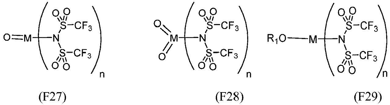

 R1 bis R5 unabhängig ausgewählt sind aus der Gruppe umfassend H, C1- bis C20-Alkyl, C1- bis C20-Heteroalkyl, unsubstituiertes oder C1- bis C12-substituiertes C6- bis C20-Aryl, unsubstituiertes oder C1- bis C12-substituiertes Heteroaryl mit 5 bis 20 ringbildenden Atomen, halogeniertes oder perhalogeniertes C1- bis C20-Alkyl, halogeniertes oder perhalogeniertes C1-bis C20-Heterolkyl, halogeniertes oder perhalogeniertes C6- bis C20-Aryl, halogeniertes oder perhalogeniertes Heteroaryl mit 5 bis 20 ringbildenden Atomen; oder wenigstens ein R1 und R4 und/oder R2 und R3 und/oder R1 und R5 verbrückt ist und einen 5- bis 20-gliedrigen cyclischen Ring bildet;wobei die fluorierten Verbindungen gemäß Formel F36 bis F46 bevorzugt sind:

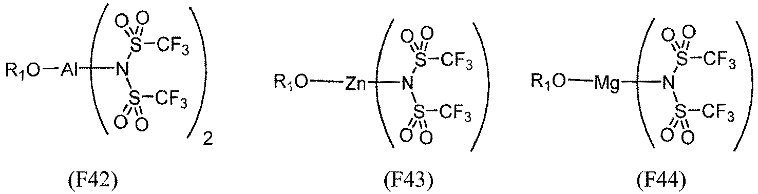

- Lochinjektionsschicht gemäß einem der Ansprüche 1 bis 14, wobei für die Triarylaminverbindung der Formel VIIa:Ar1 und Ar2 unabhängig ausgewählt sind aus Phenylen, Biphenylen, Naphthylen, Anthranylen, Carbazolylen und Fluorenylen, vorzugsweise ausgewählt aus Phenylen und Biphenylen,Ar3 bis Ar6 unabhängig ausgewählt sind aus Phenyl, Biphenyl, Terphenyl, Quartphenyl, Fluorenyl, Napthyl, Anthranyl, Phenanthryl, Thiophenyl, Fluorenyl, 9-Carbazolyl; vorzugsweiseAr3 bis Ar6 unabhängig ausgewählt sind aus Phenyl, Biphenyl, Fluorenyl, Napthyl, Thiophenyl, Fluorenyl, Carbazolyl.
- Lochinjektionsschicht gemäß einem der Ansprüche 1 bis 15, wobei die Triarylaminverbindung die Formel VIIb bis VIIk aufweist:


- Lochinjektionsschicht gemäß einem der Ansprüche 1 bis 16, wobei die Lochinjektionsschicht eine Schichtdicke von wenigstens ≥ 30 nm bis ≤ 1000 nm, vorzugsweise von ≥ 40 nm bis ≤ 500 nm, ferner bevorzugt von ≥ 50 nm bis ≤ 750 nm, aufweist.
- Lochinjektionsschicht gemäß einem der Ansprüche 1 bis 17, wobei die Lochinjektionsschicht umfasst:- wenigstens ≥ 1 Gew.-% bis ≤ 4 Gew.-%, bevorzugter ≥ 2 Gew.-% bis ≤ 3 Gew.-%, an einer ladungsneutralen Metallamidverbindung (Ia); und- wenigstens ≤ 99 Gew.-% bis ≥ 96 Gew.-%, bevorzugter ≤ 98 Gew.-% bis ≥ 97 Gew.-%, an einer Triarylaminverbindung (VIIa);wobei die Gew.-%-Werte der Komponenten auf das Gesamtgewicht der Lochinjektionsschicht bezogen sind.
- OLED (100), umfassend die Lochinjektionsschicht gemäß Ansprüchen 1 bis 18, umfassend:- eine Anode (120), eine Lochinjektionsschicht (130) und eine Emissionsschicht (150), wobei die Lochinjektionsschicht in direktem Kontakt mit der Anode steht und die Emissionsschicht in direktem Kontakt mit der Lochinjektionsschicht steht; oder- eine Anode (120), eine Lochinjektionsschicht (130), eine Lochtransportschicht (140) und eine Emissionsschicht (150), wobei die Lochinjektionsschicht in direktem Kontakt mit der Anode steht und die Lochtransportschicht in direktem Kontakt mit der Lochinjektionsschicht steht; undwobei die Zusammensetzung der Lochinjektionsschicht von der Zusammensetzung der Lochtransportschicht verschieden ist.
- Verfahren zur Herstellung einer OLED (100), wobei- die Lochinjektionsschicht (130) gemäß Ansprüchen 1 bis 18 auf eine Anodenschicht (120) aufgebracht wird, eine optionale Lochtransportschicht (140) auf die Lochinjektionsschicht (130) aufgebracht wird, eine Emissionsschicht (150) auf die Lochtransportschicht (140) aufgebracht wird, eine optionale Lochsperrschicht (155) auf die Emissionsschicht (150) aufgebracht wird, eine optionale Elektronentransportschicht (161) auf die Lochsperrschicht (155) aufgebracht wird, eine optionale Elektroneninjektionsschicht (180) auf die Elektronentransportschicht (161) aufgebracht wird und eine Kathode (190) auf die Elektroneninjektionsschicht (180) aufgebracht wird, wobei die Schichten in dieser Reihenfolge angeordnet sind und zwischen der Anode (120) und der Kathode (190) geschichtet sind;
oder- die Schichten in der umgekehrten Reihenfolge aufgebracht werden, beginnend mit der Kathode (190), und zwischen der Kathode (190) und der Anode (120) geschichtet sind.
Applications Claiming Priority (2)
| Application Number | Priority Date | Filing Date | Title |
|---|---|---|---|
| EP15181439.9A EP3133664A1 (de) | 2015-08-18 | 2015-08-18 | Mit metallamiden dotierte triarylamindickschicht zur verwendung als lochinjektionsschicht für eine organische leuchtdiode (oled) |
| PCT/EP2016/069631 WO2017029366A1 (en) | 2015-08-18 | 2016-08-18 | Triaryl amine thick layer doped with metal amides for use as hil for an organic light-emitting diode (oled) |
Publications (2)
| Publication Number | Publication Date |
|---|---|
| EP3338314A1 EP3338314A1 (de) | 2018-06-27 |
| EP3338314B1 true EP3338314B1 (de) | 2020-02-12 |
Family
ID=53900760
Family Applications (2)
| Application Number | Title | Priority Date | Filing Date |
|---|---|---|---|
| EP15181439.9A Withdrawn EP3133664A1 (de) | 2015-08-18 | 2015-08-18 | Mit metallamiden dotierte triarylamindickschicht zur verwendung als lochinjektionsschicht für eine organische leuchtdiode (oled) |
| EP16760402.4A Active EP3338314B1 (de) | 2015-08-18 | 2016-08-18 | Mit metallamiden dotierte triarylamindickschicht zur verwendung als lochinjektionsschicht für eine organische leuchtdiode (oled) |
Family Applications Before (1)
| Application Number | Title | Priority Date | Filing Date |
|---|---|---|---|
| EP15181439.9A Withdrawn EP3133664A1 (de) | 2015-08-18 | 2015-08-18 | Mit metallamiden dotierte triarylamindickschicht zur verwendung als lochinjektionsschicht für eine organische leuchtdiode (oled) |
Country Status (6)
| Country | Link |
|---|---|
| US (1) | US10998518B2 (de) |
| EP (2) | EP3133664A1 (de) |
| JP (1) | JP6807379B2 (de) |
| KR (1) | KR102658023B1 (de) |
| CN (1) | CN107925013B (de) |
| WO (1) | WO2017029366A1 (de) |
Cited By (1)
| Publication number | Priority date | Publication date | Assignee | Title |
|---|---|---|---|---|
| EP4376582A1 (de) * | 2022-11-25 | 2024-05-29 | Novaled GmbH | Organische elektrolumineszenzvorrichtung und anzeigevorrichtung mit der organischen elektrolumineszenzvorrichtung |
Families Citing this family (25)
| Publication number | Priority date | Publication date | Assignee | Title |
|---|---|---|---|---|
| EP3133663B1 (de) * | 2015-08-18 | 2022-06-15 | Novaled GmbH | Metallamide zur verwendung als lochinjektionsschicht für eine organische leuchtdiode (oled) |
| DE102015121844A1 (de) | 2015-12-15 | 2017-06-22 | Osram Oled Gmbh | Organisches elektronisches Bauelement und Verwendung eines fluorierten Sulfonimid-Metallsalzes |
| EP3364476B1 (de) * | 2017-02-20 | 2024-06-05 | Novaled GmbH | Aktive oled-anzeige, verfahren zur herstellung einer aktiven oled-anzeige und verbindung |
| EP3583636B1 (de) | 2017-02-20 | 2023-05-24 | Novaled GmbH | Elektronisches halbleiterbauteil, dessen herstellung und verbidnung |
| CN109153685B (zh) * | 2017-04-07 | 2022-11-22 | 株式会社半导体能源研究所 | 有机化合物、发光元件、发光装置、电子设备、显示装置及照明装置 |
| DE102017111137B4 (de) | 2017-05-22 | 2025-07-10 | Novaled Gmbh | Organische elektrolumineszente Vorrichtung |
| DE102017111425A1 (de) | 2017-05-24 | 2018-11-29 | Osram Oled Gmbh | Organisches elektronisches Bauelement und Verfahren zur Herstellung eines organischen elektronischen Bauelements |
| EP3503233B1 (de) * | 2017-12-20 | 2022-06-15 | Novaled GmbH | Koordinationskomplex und elektronische vorrichtung damit |
| EP3503234B1 (de) * | 2017-12-20 | 2020-11-04 | Novaled GmbH | Organische elektronische vorrichtung mit einem inversen koordinationskomplex und verfahren zur herstellung davon |
| DE102018118278B4 (de) | 2018-07-27 | 2025-02-20 | Novaled Gmbh | Elektronische Vorrichtung, Anzeigevorrichtung, Verfahren zum Herstellen derselben und eine Verbindung |
| DE102018122708B4 (de) | 2018-09-17 | 2025-02-20 | Novaled Gmbh | Organische elektronische Vorrichtung, organisches halbleitendes Material und eine Boranverbindung |
| US20210167287A1 (en) * | 2019-11-28 | 2021-06-03 | Tamotsu Horiuchi | Photoelectric conversion element, photoelectric conversion module, electronic device, and power supply module |
| EP3840081A1 (de) * | 2019-12-20 | 2021-06-23 | Novaled GmbH | Organische elektronische vorrichtung mit einer verbindung der formel (1), anzeigevorrichtung mit der organischen elektronischen vorrichtung sowie verbindungen der formel (1) zur verwendung in organischen elektronischen vorrichtungen |
| EP3840074A1 (de) * | 2019-12-20 | 2021-06-23 | Novaled GmbH | Organische elektronische vorrichtung mit einer verbindung einer formel (1), anzeigevorrichtung mit der organischen elektronischen vorrichtung sowie verbindungen einer formel (1) zur verwendung in organischen elektronischen vorrichtungen |
| EP3840076A1 (de) * | 2019-12-20 | 2021-06-23 | Novaled GmbH | Organische elektronische vorrichtung mit einer verbindung der formel (1), anzeigevorrichtung mit der organischen elektronischen vorrichtung sowie verbindungen der formel (1) zur verwendung in organischen elektronischen vorrichtungen |
| EP3840075A1 (de) * | 2019-12-20 | 2021-06-23 | Novaled GmbH | Organische elektronische vorrichtung mit einer verbindung einer formel (1), anzeigevorrichtung mit der organischen elektronischen vorrichtung sowie verbindungen einer formel (1) zur verwendung in organischen elektronischen vorrichtungen |
| EP3859811B1 (de) * | 2020-01-28 | 2025-03-19 | Novaled GmbH | Organische elektronische vorrichtung mit einer anodenschicht, einer kathodenschicht, mindestens einer emissionsschicht (eml) und mindestens einer lochinjektionsschicht (hil) |
| EP3859808B1 (de) * | 2020-01-28 | 2025-12-24 | Novaled GmbH | Organische elektronische vorrichtung mit einer lochinjektionsschicht, die eine lochtransportverbindung umfasst |
| EP3883003A1 (de) | 2020-03-20 | 2021-09-22 | Novaled GmbH | Organische elektronische vorrichtung mit einem substrat, einer anodenschicht, einer kathodenschicht, mindestens einer ersten emissionsschicht und einer lochinjektionsschicht mit einem metallkomplex |
| DE102020108402B4 (de) | 2020-03-26 | 2021-11-11 | Novaled Gmbh | Organische elektronische Vorrichtung, organisches halbleitendes Material, eine Trioxatriborinanverbindung und deren Verwendung |
| EP4002508A1 (de) * | 2020-11-16 | 2022-05-25 | Novaled GmbH | Organische elektronische vorrichtung mit einer verbindung der formel (1), anzeigevorrichtung mit der organischen elektronischen vorrichtung sowie verbindungen der formel (1) zur verwendung in organischen elektronischen vorrichtungen |
| EP4106025B1 (de) * | 2021-06-18 | 2026-04-22 | Novaled GmbH | Organische elektronische vorrichtung mit einer verbindung der formel (1), anzeigevorrichtung mit der organischen elektronischen vorrichtung sowie verbindungen der formel (1) zur verwendung in organischen elektronischen vorrichtungen |
| EP4106026A1 (de) * | 2021-06-18 | 2022-12-21 | Novaled GmbH | Organische elektronische vorrichtung mit einem substrat, einer anodenschicht, einer kathodenschicht, mindestens einer ersten emissionsschicht und mindestens einer lochinjektionsschicht mit einem metallkomplex |
| EP4106031A1 (de) * | 2021-06-18 | 2022-12-21 | Novaled GmbH | Flächenwiderstandskomponente |
| EP4356445B1 (de) * | 2021-06-18 | 2025-10-08 | Novaled GmbH | Organische elektronische vorrichtung mit einem substrat, einer anodenschicht, einer kathodenschicht, mindestens einer ersten emissionsschicht und mindestens einer lochinjektionsschicht mit einem metallkomplex |
Family Cites Families (28)
| Publication number | Priority date | Publication date | Assignee | Title |
|---|---|---|---|---|
| FR2527602A1 (fr) * | 1982-06-01 | 1983-12-02 | Anvar | Bis perhalogenoacyl- ou sulfonyl- imidures de metaux alcalins, leurs solutions solides avec des matieres plastiques et leur application a la constitution d'elements conducteurs pour des generateurs electrochimiques |
| JP3496287B2 (ja) * | 1994-09-26 | 2004-02-09 | 株式会社ユアサコーポレーション | イオン伝導性高分子化合物を用いた電池 |
| JP4876333B2 (ja) | 2000-06-08 | 2012-02-15 | 東レ株式会社 | 発光素子 |
| DE60033038T2 (de) * | 2000-11-24 | 2007-08-23 | Sony Deutschland Gmbh | Hybridsolarzelle mit thermisch abgeschiedener Halbleiteroxidschicht |
| JP4507420B2 (ja) * | 2001-02-22 | 2010-07-21 | コニカミノルタホールディングス株式会社 | 有機エレクトロルミネッセンス素子 |
| JP2003168492A (ja) * | 2001-11-26 | 2003-06-13 | Sony Internatl Europ Gmbh | 熱蒸着半導電性酸化物層を有するハイブリッド太陽電池 |
| KR100691543B1 (ko) | 2002-01-18 | 2007-03-09 | 주식회사 엘지화학 | 새로운 전자 수송용 물질 및 이를 이용한 유기 발광 소자 |
| JP2004200141A (ja) * | 2002-10-24 | 2004-07-15 | Toyota Industries Corp | 有機el素子 |
| JP4710236B2 (ja) * | 2004-03-03 | 2011-06-29 | トヨタ自動車株式会社 | 電解質組成物およびリチウム二次電池 |
| JP4900561B2 (ja) * | 2005-10-05 | 2012-03-21 | トヨタ自動車株式会社 | リチウム塩及びその利用 |
| EP1786050B1 (de) | 2005-11-10 | 2010-06-23 | Novaled AG | Dotiertes organisches Halbleitermaterial |
| JP4907200B2 (ja) * | 2006-03-09 | 2012-03-28 | 富士フイルム株式会社 | インク組成物、インクジェット記録方法、印刷物、平版印刷版の製造方法、及び、平版印刷版 |
| CN101828280B (zh) * | 2007-10-18 | 2013-03-27 | 默克专利股份有限公司 | 导电配制剂 |
| KR101111435B1 (ko) * | 2009-03-11 | 2012-02-16 | 광 석 서 | 정공주입층 및 정공수송층 재료로 사용가능한 화합물 및 이를 이용한 유기발광소자 |
| CN102421858A (zh) * | 2009-06-22 | 2012-04-18 | 默克专利有限公司 | 导电制剂 |
| KR101537654B1 (ko) * | 2010-04-22 | 2015-07-17 | 히타치가세이가부시끼가이샤 | 유기 일렉트로닉스 재료, 중합 개시제 및 열중합 개시제, 잉크 조성물, 유기 박막 및 그 제조 방법, 유기 일렉트로닉스 소자, 유기 일렉트로 루미네센스 소자, 조명 장치, 표시 소자, 및 표시 장치 |
| EP2395571B1 (de) | 2010-06-10 | 2013-12-04 | Novaled AG | Eine organische Vorrichtung umfassend ein organisches halbleitendes Material |
| EP2678346B9 (de) * | 2011-02-25 | 2018-08-08 | Ecole Polytechnique Fédérale de Lausanne (EPFL) | Metallkomplexe zur verwendung als dotierungsmittel und andere anwendungen davon |
| WO2012114315A1 (en) * | 2011-02-25 | 2012-08-30 | Ecole Polytechnique Federale De Lausanne (Epfl) | Improved redox couple for electrochemical and optoelectronic devices |
| EP2764518A1 (de) * | 2011-10-04 | 2014-08-13 | Plextronics, Inc. | Verbesserte dotierunserfahren für lochinjektion und transportschichten |
| EP2750214B1 (de) | 2011-10-05 | 2020-06-17 | LG Chem, Ltd. | Organische lichtemittierende vorrichtung und verfahren zu ihrer herstellung |
| TWI584513B (zh) | 2011-11-30 | 2017-05-21 | 諾瓦發光二極體有限公司 | 顯示器 |
| JP6015103B2 (ja) * | 2012-04-27 | 2016-10-26 | 大日本印刷株式会社 | 有機エレクトロルミネッセンス素子の製造方法 |
| EP2872590B1 (de) * | 2012-07-13 | 2018-11-14 | Merck Patent GmbH | Metallkomplexe |
| US20140116509A1 (en) * | 2012-10-30 | 2014-05-01 | Sean Andrew Vail | Solid-State Dye-Sensitized Solar Cell Using Oxidative Dopant |
| EP3052470A1 (de) * | 2013-10-02 | 2016-08-10 | Merck Patent GmbH | Lochtransportmaterialien |
| JP6166711B2 (ja) * | 2013-12-25 | 2017-07-19 | 富士フイルム株式会社 | 着色組成物、およびこれを用いた硬化膜、カラーフィルタ、パターン形成方法、カラーフィルタの製造方法、固体撮像素子および画像表示装置 |
| WO2016181911A1 (ja) * | 2015-05-08 | 2016-11-17 | 株式会社リコー | 光電変換素子 |
-
2015
- 2015-08-18 EP EP15181439.9A patent/EP3133664A1/de not_active Withdrawn
-
2016
- 2016-08-18 CN CN201680048156.4A patent/CN107925013B/zh active Active
- 2016-08-18 US US15/752,695 patent/US10998518B2/en active Active
- 2016-08-18 KR KR1020187007104A patent/KR102658023B1/ko active Active
- 2016-08-18 JP JP2018508185A patent/JP6807379B2/ja active Active
- 2016-08-18 EP EP16760402.4A patent/EP3338314B1/de active Active
- 2016-08-18 WO PCT/EP2016/069631 patent/WO2017029366A1/en not_active Ceased
Non-Patent Citations (1)
| Title |
|---|
| None * |
Cited By (2)
| Publication number | Priority date | Publication date | Assignee | Title |
|---|---|---|---|---|
| EP4376582A1 (de) * | 2022-11-25 | 2024-05-29 | Novaled GmbH | Organische elektrolumineszenzvorrichtung und anzeigevorrichtung mit der organischen elektrolumineszenzvorrichtung |
| WO2024110641A1 (en) * | 2022-11-25 | 2024-05-30 | Novaled Gmbh | Organic electroluminescent device and display device comprising the organic electroluminescent device |
Also Published As
| Publication number | Publication date |
|---|---|
| US10998518B2 (en) | 2021-05-04 |
| CN107925013B (zh) | 2020-11-10 |
| EP3133664A1 (de) | 2017-02-22 |
| US20180240995A1 (en) | 2018-08-23 |
| KR20180041695A (ko) | 2018-04-24 |
| EP3338314A1 (de) | 2018-06-27 |
| JP6807379B2 (ja) | 2021-01-06 |
| JP2018530910A (ja) | 2018-10-18 |
| KR102658023B1 (ko) | 2024-04-15 |
| CN107925013A (zh) | 2018-04-17 |
| WO2017029366A1 (en) | 2017-02-23 |
Similar Documents
| Publication | Publication Date | Title |
|---|---|---|
| US11711934B2 (en) | Metal amides for use as HIL for an organic light-emitting diode (OLED) | |
| EP3338314B1 (de) | Mit metallamiden dotierte triarylamindickschicht zur verwendung als lochinjektionsschicht für eine organische leuchtdiode (oled) | |
| EP3417495B1 (de) | Elektronentransportschicht mit einer matrixverbindungsmischung für eine organische leuchtdiode (oled) | |
| EP3235019B1 (de) | Organische leuchtdiode mit elektronentransportschichten mit unterschiedlichen matrixverbindungen | |
| EP3164898B1 (de) | Organische leuchtdiode (oled) mit einem elektronentransportschichtstapel mit unterschiedlichen lithiumverbindungen | |
| EP2999019B1 (de) | Organische Leuchtdiode (OLED) mit einem Elektronentransportschichtstapel mit unterschiedlichen Lithiumverbindungen und elementarem Metall | |
| EP3171418A1 (de) | Organische halbleiterschicht mit phosphinoxidverbindungen | |
| US10522778B2 (en) | Organic light-emitting diode including an electronic transport layer comprising a three component blend of a matrix compound and two lithium compounds |
Legal Events
| Date | Code | Title | Description |
|---|---|---|---|
| STAA | Information on the status of an ep patent application or granted ep patent |
Free format text: STATUS: UNKNOWN |
|
| STAA | Information on the status of an ep patent application or granted ep patent |
Free format text: STATUS: THE INTERNATIONAL PUBLICATION HAS BEEN MADE |
|
| PUAI | Public reference made under article 153(3) epc to a published international application that has entered the european phase |
Free format text: ORIGINAL CODE: 0009012 |
|
| STAA | Information on the status of an ep patent application or granted ep patent |
Free format text: STATUS: REQUEST FOR EXAMINATION WAS MADE |
|
| 17P | Request for examination filed |
Effective date: 20180308 |
|
| AK | Designated contracting states |
Kind code of ref document: A1 Designated state(s): AL AT BE BG CH CY CZ DE DK EE ES FI FR GB GR HR HU IE IS IT LI LT LU LV MC MK MT NL NO PL PT RO RS SE SI SK SM TR |
|
| AX | Request for extension of the european patent |
Extension state: BA ME |
|
| DAV | Request for validation of the european patent (deleted) | ||
| DAX | Request for extension of the european patent (deleted) | ||
| GRAP | Despatch of communication of intention to grant a patent |
Free format text: ORIGINAL CODE: EPIDOSNIGR1 |
|
| STAA | Information on the status of an ep patent application or granted ep patent |
Free format text: STATUS: GRANT OF PATENT IS INTENDED |
|
| INTG | Intention to grant announced |
Effective date: 20190830 |
|
| GRAS | Grant fee paid |
Free format text: ORIGINAL CODE: EPIDOSNIGR3 |
|
| GRAA | (expected) grant |
Free format text: ORIGINAL CODE: 0009210 |
|
| STAA | Information on the status of an ep patent application or granted ep patent |
Free format text: STATUS: THE PATENT HAS BEEN GRANTED |
|
| AK | Designated contracting states |
Kind code of ref document: B1 Designated state(s): AL AT BE BG CH CY CZ DE DK EE ES FI FR GB GR HR HU IE IS IT LI LT LU LV MC MK MT NL NO PL PT RO RS SE SI SK SM TR |
|
| RAP1 | Party data changed (applicant data changed or rights of an application transferred) |
Owner name: NOVALED GMBH |
|
| REG | Reference to a national code |
Ref country code: GB Ref legal event code: FG4D |
|
| REG | Reference to a national code |
Ref country code: CH Ref legal event code: EP |
|
| REG | Reference to a national code |
Ref country code: AT Ref legal event code: REF Ref document number: 1233269 Country of ref document: AT Kind code of ref document: T Effective date: 20200215 |
|
| REG | Reference to a national code |
Ref country code: IE Ref legal event code: FG4D |
|
| REG | Reference to a national code |
Ref country code: DE Ref legal event code: R096 Ref document number: 602016029599 Country of ref document: DE |
|
| PG25 | Lapsed in a contracting state [announced via postgrant information from national office to epo] |
Ref country code: NO Free format text: LAPSE BECAUSE OF FAILURE TO SUBMIT A TRANSLATION OF THE DESCRIPTION OR TO PAY THE FEE WITHIN THE PRESCRIBED TIME-LIMIT Effective date: 20200512 Ref country code: RS Free format text: LAPSE BECAUSE OF FAILURE TO SUBMIT A TRANSLATION OF THE DESCRIPTION OR TO PAY THE FEE WITHIN THE PRESCRIBED TIME-LIMIT Effective date: 20200212 Ref country code: FI Free format text: LAPSE BECAUSE OF FAILURE TO SUBMIT A TRANSLATION OF THE DESCRIPTION OR TO PAY THE FEE WITHIN THE PRESCRIBED TIME-LIMIT Effective date: 20200212 |
|
| REG | Reference to a national code |
Ref country code: LT Ref legal event code: MG4D |
|
| REG | Reference to a national code |
Ref country code: NL Ref legal event code: MP Effective date: 20200212 |
|
| PG25 | Lapsed in a contracting state [announced via postgrant information from national office to epo] |
Ref country code: HR Free format text: LAPSE BECAUSE OF FAILURE TO SUBMIT A TRANSLATION OF THE DESCRIPTION OR TO PAY THE FEE WITHIN THE PRESCRIBED TIME-LIMIT Effective date: 20200212 Ref country code: GR Free format text: LAPSE BECAUSE OF FAILURE TO SUBMIT A TRANSLATION OF THE DESCRIPTION OR TO PAY THE FEE WITHIN THE PRESCRIBED TIME-LIMIT Effective date: 20200513 Ref country code: BG Free format text: LAPSE BECAUSE OF FAILURE TO SUBMIT A TRANSLATION OF THE DESCRIPTION OR TO PAY THE FEE WITHIN THE PRESCRIBED TIME-LIMIT Effective date: 20200512 Ref country code: LV Free format text: LAPSE BECAUSE OF FAILURE TO SUBMIT A TRANSLATION OF THE DESCRIPTION OR TO PAY THE FEE WITHIN THE PRESCRIBED TIME-LIMIT Effective date: 20200212 Ref country code: SE Free format text: LAPSE BECAUSE OF FAILURE TO SUBMIT A TRANSLATION OF THE DESCRIPTION OR TO PAY THE FEE WITHIN THE PRESCRIBED TIME-LIMIT Effective date: 20200212 Ref country code: IS Free format text: LAPSE BECAUSE OF FAILURE TO SUBMIT A TRANSLATION OF THE DESCRIPTION OR TO PAY THE FEE WITHIN THE PRESCRIBED TIME-LIMIT Effective date: 20200612 |
|
| PG25 | Lapsed in a contracting state [announced via postgrant information from national office to epo] |
Ref country code: NL Free format text: LAPSE BECAUSE OF FAILURE TO SUBMIT A TRANSLATION OF THE DESCRIPTION OR TO PAY THE FEE WITHIN THE PRESCRIBED TIME-LIMIT Effective date: 20200212 |
|
| PG25 | Lapsed in a contracting state [announced via postgrant information from national office to epo] |
Ref country code: CZ Free format text: LAPSE BECAUSE OF FAILURE TO SUBMIT A TRANSLATION OF THE DESCRIPTION OR TO PAY THE FEE WITHIN THE PRESCRIBED TIME-LIMIT Effective date: 20200212 Ref country code: RO Free format text: LAPSE BECAUSE OF FAILURE TO SUBMIT A TRANSLATION OF THE DESCRIPTION OR TO PAY THE FEE WITHIN THE PRESCRIBED TIME-LIMIT Effective date: 20200212 Ref country code: SK Free format text: LAPSE BECAUSE OF FAILURE TO SUBMIT A TRANSLATION OF THE DESCRIPTION OR TO PAY THE FEE WITHIN THE PRESCRIBED TIME-LIMIT Effective date: 20200212 Ref country code: DK Free format text: LAPSE BECAUSE OF FAILURE TO SUBMIT A TRANSLATION OF THE DESCRIPTION OR TO PAY THE FEE WITHIN THE PRESCRIBED TIME-LIMIT Effective date: 20200212 Ref country code: PT Free format text: LAPSE BECAUSE OF FAILURE TO SUBMIT A TRANSLATION OF THE DESCRIPTION OR TO PAY THE FEE WITHIN THE PRESCRIBED TIME-LIMIT Effective date: 20200705 Ref country code: ES Free format text: LAPSE BECAUSE OF FAILURE TO SUBMIT A TRANSLATION OF THE DESCRIPTION OR TO PAY THE FEE WITHIN THE PRESCRIBED TIME-LIMIT Effective date: 20200212 Ref country code: LT Free format text: LAPSE BECAUSE OF FAILURE TO SUBMIT A TRANSLATION OF THE DESCRIPTION OR TO PAY THE FEE WITHIN THE PRESCRIBED TIME-LIMIT Effective date: 20200212 Ref country code: SM Free format text: LAPSE BECAUSE OF FAILURE TO SUBMIT A TRANSLATION OF THE DESCRIPTION OR TO PAY THE FEE WITHIN THE PRESCRIBED TIME-LIMIT Effective date: 20200212 Ref country code: EE Free format text: LAPSE BECAUSE OF FAILURE TO SUBMIT A TRANSLATION OF THE DESCRIPTION OR TO PAY THE FEE WITHIN THE PRESCRIBED TIME-LIMIT Effective date: 20200212 |
|
| REG | Reference to a national code |
Ref country code: DE Ref legal event code: R097 Ref document number: 602016029599 Country of ref document: DE |
|
| REG | Reference to a national code |
Ref country code: AT Ref legal event code: MK05 Ref document number: 1233269 Country of ref document: AT Kind code of ref document: T Effective date: 20200212 |
|
| PLBE | No opposition filed within time limit |
Free format text: ORIGINAL CODE: 0009261 |
|
| STAA | Information on the status of an ep patent application or granted ep patent |
Free format text: STATUS: NO OPPOSITION FILED WITHIN TIME LIMIT |
|
| 26N | No opposition filed |
Effective date: 20201113 |
|
| PG25 | Lapsed in a contracting state [announced via postgrant information from national office to epo] |
Ref country code: AT Free format text: LAPSE BECAUSE OF FAILURE TO SUBMIT A TRANSLATION OF THE DESCRIPTION OR TO PAY THE FEE WITHIN THE PRESCRIBED TIME-LIMIT Effective date: 20200212 Ref country code: IT Free format text: LAPSE BECAUSE OF FAILURE TO SUBMIT A TRANSLATION OF THE DESCRIPTION OR TO PAY THE FEE WITHIN THE PRESCRIBED TIME-LIMIT Effective date: 20200212 |
|
| PG25 | Lapsed in a contracting state [announced via postgrant information from national office to epo] |
Ref country code: PL Free format text: LAPSE BECAUSE OF FAILURE TO SUBMIT A TRANSLATION OF THE DESCRIPTION OR TO PAY THE FEE WITHIN THE PRESCRIBED TIME-LIMIT Effective date: 20200212 Ref country code: SI Free format text: LAPSE BECAUSE OF FAILURE TO SUBMIT A TRANSLATION OF THE DESCRIPTION OR TO PAY THE FEE WITHIN THE PRESCRIBED TIME-LIMIT Effective date: 20200212 |
|
| PG25 | Lapsed in a contracting state [announced via postgrant information from national office to epo] |
Ref country code: MC Free format text: LAPSE BECAUSE OF FAILURE TO SUBMIT A TRANSLATION OF THE DESCRIPTION OR TO PAY THE FEE WITHIN THE PRESCRIBED TIME-LIMIT Effective date: 20200212 |
|
| REG | Reference to a national code |
Ref country code: CH Ref legal event code: PL |
|
| GBPC | Gb: european patent ceased through non-payment of renewal fee |
Effective date: 20200818 |
|
| PG25 | Lapsed in a contracting state [announced via postgrant information from national office to epo] |
Ref country code: LU Free format text: LAPSE BECAUSE OF NON-PAYMENT OF DUE FEES Effective date: 20200818 Ref country code: LI Free format text: LAPSE BECAUSE OF NON-PAYMENT OF DUE FEES Effective date: 20200831 Ref country code: CH Free format text: LAPSE BECAUSE OF NON-PAYMENT OF DUE FEES Effective date: 20200831 |
|
| REG | Reference to a national code |
Ref country code: BE Ref legal event code: MM Effective date: 20200831 |
|
| PG25 | Lapsed in a contracting state [announced via postgrant information from national office to epo] |
Ref country code: FR Free format text: LAPSE BECAUSE OF NON-PAYMENT OF DUE FEES Effective date: 20200831 |
|
| PG25 | Lapsed in a contracting state [announced via postgrant information from national office to epo] |
Ref country code: IE Free format text: LAPSE BECAUSE OF NON-PAYMENT OF DUE FEES Effective date: 20200818 Ref country code: GB Free format text: LAPSE BECAUSE OF NON-PAYMENT OF DUE FEES Effective date: 20200818 Ref country code: BE Free format text: LAPSE BECAUSE OF NON-PAYMENT OF DUE FEES Effective date: 20200831 |
|
| PG25 | Lapsed in a contracting state [announced via postgrant information from national office to epo] |
Ref country code: TR Free format text: LAPSE BECAUSE OF FAILURE TO SUBMIT A TRANSLATION OF THE DESCRIPTION OR TO PAY THE FEE WITHIN THE PRESCRIBED TIME-LIMIT Effective date: 20200212 Ref country code: MT Free format text: LAPSE BECAUSE OF FAILURE TO SUBMIT A TRANSLATION OF THE DESCRIPTION OR TO PAY THE FEE WITHIN THE PRESCRIBED TIME-LIMIT Effective date: 20200212 Ref country code: CY Free format text: LAPSE BECAUSE OF FAILURE TO SUBMIT A TRANSLATION OF THE DESCRIPTION OR TO PAY THE FEE WITHIN THE PRESCRIBED TIME-LIMIT Effective date: 20200212 |
|
| PG25 | Lapsed in a contracting state [announced via postgrant information from national office to epo] |
Ref country code: MK Free format text: LAPSE BECAUSE OF FAILURE TO SUBMIT A TRANSLATION OF THE DESCRIPTION OR TO PAY THE FEE WITHIN THE PRESCRIBED TIME-LIMIT Effective date: 20200212 Ref country code: AL Free format text: LAPSE BECAUSE OF FAILURE TO SUBMIT A TRANSLATION OF THE DESCRIPTION OR TO PAY THE FEE WITHIN THE PRESCRIBED TIME-LIMIT Effective date: 20200212 |
|
| REG | Reference to a national code |
Ref country code: DE Ref legal event code: R079 Ref document number: 602016029599 Country of ref document: DE Free format text: PREVIOUS MAIN CLASS: H01L0051540000 Ipc: H10K0085000000 |
|
| P01 | Opt-out of the competence of the unified patent court (upc) registered |
Effective date: 20230526 |
|
| PGFP | Annual fee paid to national office [announced via postgrant information from national office to epo] |
Ref country code: DE Payment date: 20250624 Year of fee payment: 10 |