EP3339886B1 - Récepteur de lumière comprenant une pluralité d'éléments à photodiode à avalanche et procédé d'alimentation en pré-tension - Google Patents
Récepteur de lumière comprenant une pluralité d'éléments à photodiode à avalanche et procédé d'alimentation en pré-tension Download PDFInfo
- Publication number
- EP3339886B1 EP3339886B1 EP16206061.0A EP16206061A EP3339886B1 EP 3339886 B1 EP3339886 B1 EP 3339886B1 EP 16206061 A EP16206061 A EP 16206061A EP 3339886 B1 EP3339886 B1 EP 3339886B1
- Authority
- EP
- European Patent Office
- Prior art keywords
- bias
- light receiver
- voltage
- avalanche photodiode
- bias voltage
- Prior art date
- Legal status (The legal status is an assumption and is not a legal conclusion. Google has not performed a legal analysis and makes no representation as to the accuracy of the status listed.)
- Active
Links
Images


Classifications
-
- G—PHYSICS
- G01—MEASURING; TESTING
- G01J—MEASUREMENT OF INTENSITY, VELOCITY, SPECTRAL CONTENT, POLARISATION, PHASE OR PULSE CHARACTERISTICS OF INFRARED, VISIBLE OR ULTRAVIOLET LIGHT; COLORIMETRY; RADIATION PYROMETRY
- G01J1/00—Photometry, e.g. photographic exposure meter
- G01J1/42—Photometry, e.g. photographic exposure meter using electric radiation detectors
- G01J1/44—Electric circuits
-
- G—PHYSICS
- G01—MEASURING; TESTING
- G01J—MEASUREMENT OF INTENSITY, VELOCITY, SPECTRAL CONTENT, POLARISATION, PHASE OR PULSE CHARACTERISTICS OF INFRARED, VISIBLE OR ULTRAVIOLET LIGHT; COLORIMETRY; RADIATION PYROMETRY
- G01J1/00—Photometry, e.g. photographic exposure meter
- G01J1/42—Photometry, e.g. photographic exposure meter using electric radiation detectors
- G01J1/44—Electric circuits
- G01J1/46—Electric circuits using a capacitor
-
- G—PHYSICS
- G01—MEASURING; TESTING
- G01S—RADIO DIRECTION-FINDING; RADIO NAVIGATION; DETERMINING DISTANCE OR VELOCITY BY USE OF RADIO WAVES; LOCATING OR PRESENCE-DETECTING BY USE OF THE REFLECTION OR RERADIATION OF RADIO WAVES; ANALOGOUS ARRANGEMENTS USING OTHER WAVES
- G01S7/00—Details of systems according to groups G01S13/00, G01S15/00, G01S17/00
- G01S7/48—Details of systems according to groups G01S13/00, G01S15/00, G01S17/00 of systems according to group G01S17/00
- G01S7/483—Details of pulse systems
- G01S7/486—Receivers
- G01S7/4861—Circuits for detection, sampling, integration or read-out
- G01S7/4863—Detector arrays, e.g. charge-transfer gates
-
- G—PHYSICS
- G01—MEASURING; TESTING
- G01S—RADIO DIRECTION-FINDING; RADIO NAVIGATION; DETERMINING DISTANCE OR VELOCITY BY USE OF RADIO WAVES; LOCATING OR PRESENCE-DETECTING BY USE OF THE REFLECTION OR RERADIATION OF RADIO WAVES; ANALOGOUS ARRANGEMENTS USING OTHER WAVES
- G01S7/00—Details of systems according to groups G01S13/00, G01S15/00, G01S17/00
- G01S7/48—Details of systems according to groups G01S13/00, G01S15/00, G01S17/00 of systems according to group G01S17/00
- G01S7/497—Means for monitoring or calibrating
-
- G—PHYSICS
- G01—MEASURING; TESTING
- G01J—MEASUREMENT OF INTENSITY, VELOCITY, SPECTRAL CONTENT, POLARISATION, PHASE OR PULSE CHARACTERISTICS OF INFRARED, VISIBLE OR ULTRAVIOLET LIGHT; COLORIMETRY; RADIATION PYROMETRY
- G01J1/00—Photometry, e.g. photographic exposure meter
- G01J1/42—Photometry, e.g. photographic exposure meter using electric radiation detectors
- G01J1/44—Electric circuits
- G01J2001/4406—Plural ranges in circuit, e.g. switchable ranges; Adjusting sensitivity selecting gain values
-
- G—PHYSICS
- G01—MEASURING; TESTING
- G01J—MEASUREMENT OF INTENSITY, VELOCITY, SPECTRAL CONTENT, POLARISATION, PHASE OR PULSE CHARACTERISTICS OF INFRARED, VISIBLE OR ULTRAVIOLET LIGHT; COLORIMETRY; RADIATION PYROMETRY
- G01J1/00—Photometry, e.g. photographic exposure meter
- G01J1/42—Photometry, e.g. photographic exposure meter using electric radiation detectors
- G01J1/44—Electric circuits
- G01J2001/4446—Type of detector
- G01J2001/446—Photodiode
- G01J2001/4466—Avalanche
-
- G—PHYSICS
- G01—MEASURING; TESTING
- G01J—MEASUREMENT OF INTENSITY, VELOCITY, SPECTRAL CONTENT, POLARISATION, PHASE OR PULSE CHARACTERISTICS OF INFRARED, VISIBLE OR ULTRAVIOLET LIGHT; COLORIMETRY; RADIATION PYROMETRY
- G01J1/00—Photometry, e.g. photographic exposure meter
- G01J1/42—Photometry, e.g. photographic exposure meter using electric radiation detectors
- G01J1/44—Electric circuits
- G01J2001/4446—Type of detector
- G01J2001/448—Array [CCD]
-
- G—PHYSICS
- G01—MEASURING; TESTING
- G01S—RADIO DIRECTION-FINDING; RADIO NAVIGATION; DETERMINING DISTANCE OR VELOCITY BY USE OF RADIO WAVES; LOCATING OR PRESENCE-DETECTING BY USE OF THE REFLECTION OR RERADIATION OF RADIO WAVES; ANALOGOUS ARRANGEMENTS USING OTHER WAVES
- G01S17/00—Systems using the reflection or reradiation of electromagnetic waves other than radio waves, e.g. lidar systems
- G01S17/02—Systems using the reflection of electromagnetic waves other than radio waves
- G01S17/06—Systems determining position data of a target
- G01S17/08—Systems determining position data of a target for measuring distance only
-
- G—PHYSICS
- G01—MEASURING; TESTING
- G01S—RADIO DIRECTION-FINDING; RADIO NAVIGATION; DETERMINING DISTANCE OR VELOCITY BY USE OF RADIO WAVES; LOCATING OR PRESENCE-DETECTING BY USE OF THE REFLECTION OR RERADIATION OF RADIO WAVES; ANALOGOUS ARRANGEMENTS USING OTHER WAVES
- G01S17/00—Systems using the reflection or reradiation of electromagnetic waves other than radio waves, e.g. lidar systems
- G01S17/88—Lidar systems specially adapted for specific applications
- G01S17/89—Lidar systems specially adapted for specific applications for mapping or imaging
-
- G—PHYSICS
- G01—MEASURING; TESTING
- G01S—RADIO DIRECTION-FINDING; RADIO NAVIGATION; DETERMINING DISTANCE OR VELOCITY BY USE OF RADIO WAVES; LOCATING OR PRESENCE-DETECTING BY USE OF THE REFLECTION OR RERADIATION OF RADIO WAVES; ANALOGOUS ARRANGEMENTS USING OTHER WAVES
- G01S7/00—Details of systems according to groups G01S13/00, G01S15/00, G01S17/00
- G01S7/48—Details of systems according to groups G01S13/00, G01S15/00, G01S17/00 of systems according to group G01S17/00
- G01S7/481—Constructional features, e.g. arrangements of optical elements
- G01S7/4816—Constructional features, e.g. arrangements of optical elements of receivers alone
Definitions
- the invention relates to a light receiver with a plurality of avalanche photodiode elements and a method for supplying it with a bias according to the preamble of claim 1 and 15, respectively.
- a light receiver has the function of generating an electrical signal from incident receiving light.
- the detection sensitivity of simple photodiodes is not sufficient in many applications.
- an avalanche photodiode Avalanche Photo Diode
- the incident light triggers a controlled avalanche effect.
- the charge carriers generated by incident photons are multiplied, and a photocurrent is produced which is proportional to the light reception intensity but much larger than that of a simple PIN diode.
- the avalanche photodiode is biased above the breakdown voltage (bias), so that even a single, released by a single photon charge carrier can trigger an avalanche, which then recruits all available charge carriers due to the high field strength.
- the avalanche photodiode thus counts as the eponymous Geiger counter individual events.
- Avalanche photodiodes in Geiger mode are also referred to as SPADs (Single-Photon Avalanche Diode).
- SPADs The high radiation sensitivity of SPADs is used in many applications. These include medical technology with CT, MRI or blood analysis, optical metrology including spectroscopy, distance measurement and three-dimensional imaging, radiation detection in nuclear physics or uses in telescopes for astrophysics.
- Geiger APDS or SPADs are very fast, high-sensitivity photodiodes based on semiconductors.
- a disadvantage of the high sensitivity is that not only a Nutzlichtphoton, but also a weak interference event by extraneous light, optical crosstalk or dark noise can trigger the avalanche breakdown. This interference event then contributes the same relatively strong signal to the measurement result as the received useful light and can not be distinguished from the signal. Subsequently, the avalanche photodiode remains insensitive for a dead time of about 5 to 100 ns and drops out for further measurements. Therefore, it is common to interconnect and statistically evaluate multiple SPADs. Nevertheless, larger light outputs lead to supersaturation effects of individual pixels or entire areas. Especially when a large dynamic range is to be covered, so important information about the received light can be lost.
- the breakdown voltage is the minimum required bias to maintain the desired Geiger mode for a SPAD. Strictly speaking, however, the detection efficiency and the gain are still zero at this limit. Only when the bias voltage exceeds the breakdown voltage, incident photons are converted into corresponding Geigerstromimpulse. At an ideal photon detection efficiency (PDE) of 100%, each incident photon would trigger a geiger current impulse. Practically this does not succeed completely. However, the PDE may be affected by the amount of bias applied.
- the anode and cathode-side connections of the individual SPAD cells of the light receiver are led out directly.
- all SPADs are operated with a common bias voltage. Instead of the bias usually only the overvoltage, so the difference between bias and breakdown voltage is considered.
- the triggering probability increases with the overvoltage. There is in practice a reasonable upper limit, because the probability of tripping at higher surges in limiting and unwanted noise components increase disproportionately with.
- the operating point set by means of overvoltage allows a certain adaptation of the light receiver, but does not do justice to many situations with greatly varying or temporally fluctuating received light conditions.
- the WO 2011/117309 A2 Proposes to provide, in addition to the anode and cathode for the application of the bias voltage, a third electrode to the SPAD detector, via which the Geigerstrom is capacitively coupled. This is to prevent the readout being delayed by switching elements of the bias voltage. An improved adaptation of the light receiver to ambient or application conditions is not given by this.
- the US 2013/0153754 A1 discloses an apparatus for distance measurement according to a light transit time method comprising a light receiver having a plurality of SPADs.
- the aim is to limit the power consumption by actually supplying only a portion of the SPADs with a bias voltage above the breakdown voltage.
- the high-voltage power supply has a plurality of lines which are each connected to individual or group SPADs. By means of a switching control unit, it can be selectively decided which of the lines transmit the high voltage.
- the pixels of the light sensor are designed as SPADs.
- a controller monitors the intensity of the incident light. If it is too weak, it will switch from a linear mode to a Geiger mode by operating the SPADs with a bias voltage above the breakdown voltage. If the light is too strong, it reverses to the linear mode.
- the respective required bias voltage is provided by a bias unit.
- the DE 20 2013 105 389 U1 describes an optoelectronic sensor with avalanche photodiode elements operated in Geiger mode.
- the sensor comprises a temperature measuring element, which may be part of the same integrated circuit with further functional elements such as the light receiver or the evaluation unit.
- a temperature compensation for example, the supply voltage allows.
- a light receiver having a plurality of avalanche photodiode elements and a method for supplying them with a bias voltage Claim 1 or 15 solved.
- a bias voltage above the breakdown voltage is applied to the avalanche photodiode elements, they operate in Geiger mode.
- the invention is based on the basic idea of locally adapting the bias voltage and thus the detection sensitivity.
- a plurality of different bias voltages are available on the light receiver, which are provided from the outside or by a circuit of the light receiver to bias terminals for avalanche photodiode elements.
- the avalanche photodiode elements in turn are subdivided into a plurality, that is to say at least two groups whose size can be determined as required, up to only one avalanche photodiode element in each case.
- the associated avalanche photodiode elements are supplied with one of the different bias voltages, and therefore the groups are different sensitive.
- the number of available biases and groups is basically independent of each other, and multiple groups can be supplied with the same bias, and also no available bias can be used by any group.
- the invention has the advantage that the light receiver is much more flexible use. This enables a cost reduction due to less variant diversity and higher quantities.
- the light receiver will also be much more robust against changing environmental conditions.
- the locally varying biases act as a customizable electronic shutter, which specifically ensures inhomogeneous sensitivity of the light receiver by electronically fading out reception areas or deliberately attenuating their signals. This is the optics design, thus the tasks are substantially simplified, for example by omitting apertures or less complex lenses are used. This also supports further miniaturization of a sensor in which the light receiver is used, and there is greater freedom in placing components.
- the light receiver already has the electronic possibility of dealing with a high dynamic range and inhomogeneities of the receiving light through the electronic shutter.
- an electronic receive adjustment is possible by the local sensitivity is adjusted electronically to the circumstances with only rough mechanical adjustment, for example, an electronic shutter is placed around a receiving light spot. This requires no mechanical or manual device intervention, no mechanical protection against misalignment, not even an accessibility of the device, and is easier to automate.
- the integration of the avalanche photodiode elements on a photoreceptor, in contrast to discrete avalanche photodiode elements, allows much more arrangements in which unused non-photosensitive interregions and assembly tolerances between the discrete components are eliminated.
- the avalanche photodiode elements of a group are preferably optionally supplied with one of the different bias voltages. This makes the adaptability to certain lighting conditions or applications flexible.
- the choice of which group is supplied with which bias means a configuration or reconfiguration and can be done at various times, be it by selecting between predetermined modes, already at the factory, during commissioning or dynamically during operation.
- An example of application is a dimming, ie deactivation or damping by a lower bias, for avalanche photodiode elements in an area which is otherwise overdriven by too much light.
- a switching element is preferably arranged.
- This switching element is a means of choosing a bias for a group.
- the switching element is preferably a multiple switch between not only two, but several or all of the available different bias voltages.
- the switching element can be coded, in particular work binary coded to get along with as few switches as possible even with a slightly larger number of available bias voltages.
- At least two of the plurality of bias terminals are preferably led to the outside.
- all bias connections are led to the outside.
- external different bias voltages can be provided.
- External bias connections allow a very simple circuit concept, where the connections and the bias voltages are accessible and controllable from the outside.
- At least one of the bias terminals is preferably internal, with at least one voltage adjustment element being provided to generate different bias voltages from an external voltage.
- the voltage adjustment element adjusts the external bias voltage by a differential voltage, and more bias voltages are produced with other voltage adjustment elements or multiple differential voltages.
- the external voltage can be used as such as one of the different bias voltages, in particular by selecting a differential voltage zero.
- a mixed form with a plurality of outwardly biased bias terminals is conceivable, but preferably all bias terminals are internal. Then, only a single external voltage is required to dissipate all of the biases and thus provide internally, resulting in significant savings in external circuitry costs with space and cost advantages.
- the voltage adjustment element is preferably designed to be stress-relieving. Then, preferably, an external voltage is applied to the light receiver which is too high or corresponds to the highest required bias voltage in order to provide sufficient reserve for the voltage extraction. Circuit technology, it is particularly easy if the compensation is always done by voltage. But it would also be possible alternatively, if one takes the increased effort into account, a positive compensation, which raises the externally applied bias, such as a charge pump.
- the voltage adjustment element preferably has a drive in order to set the bias voltage to be generated.
- This control is particularly accessible from the outside, for example as a digital control.
- the values of the different bias voltages available become variable, and this can be used to provide appropriate levels of sensitivity, but also to adjust the sensitivity of the avalanche photodiode elements associated with the respective bias voltage.
- the avalanche photodiode elements of at least one group are preferably fixedly connected to a respective bias terminal. Again, preferably, all groups are firmly connected to a bias connection. This results in a simpler design of the light receiver, but at the same time reduces the variability. An adjustment is possible here only by lowering or raising the bias voltage to the bias terminals.
- the groups preferably form a checkerboard pattern, a concentric pattern or a plurality of laterally displaced regions. These are some advantageous examples of a division into more sensitive and insensitive areas, the patterns depending on the embodiment, by hard wiring or dynamic interconnection of matching groups to a respective same bias.
- the pattern, together with the associated bias levels, defines the behavior of the electronic shutter, whereby shutter patterns are conceivable that would be difficult or impossible to realize with optical elements.
- a checkerboard pattern is representative of a pattern in which both more sensitive and less sensitive avalanche photodiode elements are available locally alternately. Thus, a measurement with much and little signal can be done simultaneously, without loss of time, which would result in a conventional sweeping through the sensitivity (sweep / step).
- a concentric pattern is suitable for a spot of light whose size is distance-dependent, or which comes in and out of focus during relative object movement.
- An example of a lateral shift is the unavoidable shift in a biaxial transmit and receive path, which is even the desired measurement effect in triangulation methods. It is also conceivable to use several areas for a plurality of measuring channels, for example a measuring channel and a reference channel or areas for a plurality of transmitters with different properties, in particular wavelengths.
- At least one bias terminal preferably provides a bias above and a bias terminal provides a bias below the breakdown voltage. This allows the Geiger mode to be switched on and off as desired. The is practically synonymous with turning on and off the light reception, since the gain in the Geiger mode is in the order of 10 6 .
- the bias terminals preferably provide different overvoltages above the breakdown voltage. With the overvoltage, the gain and the probability of triggering of the avalanche photodiode elements are related. Thus, an electronic dazzling effect can be achieved not only binary in the sense of a shutdown when the bias voltage is below the breakdown voltage, but it is a gradual attenuation corresponding to a only damping aperture with intermediate stages possible.
- at least one bias below the breakdown voltage and several different overvoltages are available at the bias terminals in a hybrid form.
- the light receiver preferably has a plurality of bias potential different positive potential terminals and a plurality of negative potential bias terminals for supplying avalanche photodiode elements with a positive potential and a negative potential having different biases by connecting both sides thereof.
- the terms positive and negative are relatively relative to potentials.
- the point of reference is the situation that, as in many other embodiments, the avalanche photodiode elements are supplied with different potentials from only one side, and thus the bias voltage to ground is defined. In contrast, the additional variable potential introduced here on the opposite side is then negative.
- the groups preferably form a matrix array and the positive potential bias terminals are each connected to one row or column and correspondingly the negative potential bias terminals are connected to one column or row.
- Each such pixel can now be individually supplied by row and column drive with a different bias voltage. In particular, this allows targeted, only one Operate group or certain areas of the matrix above the breakdown voltage. In this way, a detection event can be localized on the matrix without any special requirements for the readout of the light receiver.
- the light receiver preferably has at least one temperature detection element for detecting an operating temperature of the avalanche photodiode elements and a temperature compensation unit which adjusts the bias voltages as a function of the measured temperature.
- the breakdown voltage is subject to a temperature dependence of the order of 20-30 mV / K and therefore has a very noticeable effect on the effective effect of applied bias over a typical temperature range.
- the temperature sensing element determines the operating temperature, wherein the measurement is not necessarily carried out in a conventional unit such as ° C or K, but for example, may also be a temperature-dependent raw information such as a voltage or a current in the temperature sensing element.
- a temperature compensation unit then adjusts the bias voltages according to the measurement information of the temperature detection element. This additional modification of the bias voltages is possible with very little effort and then ensures that fluctuations over the operating temperature are balanced.
- the temperature sensing element is preferably integrated on the light receiver and arises in particular in the same semiconductor process with the avalanche photodiode elements. This results in a very compact and accurate temperature compensation. Still preferably, the temperature sensing element comprises at least one of the avalanche photodiode elements. This directly uses the same temperature dependence for the determination of the operating temperature, which is then compensated.
- An avalanche photodiode element which measures the temperature is preferably blind, which means at least that its signal does not contribute to the useful signal of the light receiver and may also mean that such avalanche photodiode element is optically shielded and possibly also electrically isolated. Otherwise your own activity could falsify the temperature measurement.
- the temperature compensation unit preferably acts on the at least one voltage adjustment element.
- a further, temperature-dependent voltage difference is taken into account there.
- at least one additional voltage-changing preferably provide withdrawing element for the temperature-dependent voltage difference.
- the temperature compensation unit preferably adjusts all biases simultaneously on a common path. In this case, one element is sufficient to compensate for all bias voltages as a function of the temperature.
- the temperature compensation unit can be arranged in particular with respect to the voltage adjustment for the different bias voltages.
- the light receiver preferably has an active current limiting unit which lowers the bias voltages when a current threshold of the current flowing in the light receiver is exceeded.
- the current limiting unit can preferably lower all bias voltages at the same time on a common path.
- the current limiting is preferably integrated in the light receiver, protects it from damage and ensures even during the current-limited operation for a meaningful operating point.
- the temperature compensation unit preferably simultaneously acts as a current-limiting unit. Because the current flowing in the light receiver depends on the bias voltage. Thus, already funds are available to limit the power anyway. Due to their dual function, there is virtually no additional effort.
- the current threshold can also be adapted to the operating temperature, because at lower operating temperature, the light receiver holds larger currents without being damaged or unreliable by too much activity with subsequent dead times of the avalanche photodiode elements. Since the temperature compensation unit has access to the operating temperature anyway, it can very easily take this into account and adjust the current threshold from which the bias voltage for limiting the current must be lowered.
- an optoelectronic sensor is provided with at least one light receiver according to the invention, wherein the sensor is designed for distance measurement according to a light transit time method and / or as a code reader and / or for data transmission.
- the distance can be determined by triangulation, such as in a triangulation stylus or a stereo camera.
- the distance measurement preferably takes place according to a light transit time method.
- a pulse transit time method a short light pulse is emitted with a light transmitter and the time until reception of a remission or reflection of the light pulse is measured.
- transmitted light is amplitude modulated and a phase shift determined between the transmitted and received light, wherein the phase shift is also a measure of the light transit time.
- the light transit time method can be used in a one-dimensional distance sensor, a laser scanner or an image sensor of a 3D camera according to the light transit time principle.
- Other non-terminating applications of the light receiver in an optoelectronic sensor are code reading or data transmission, or combinations of these applications in a sensor.
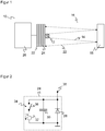
- FIG. 1 shows a schematic representation of an optoelectronic sensor 10 in one embodiment as a single-beam light sensor.
- a light emitter 12 for example an LED or a laser light source, emits a light signal 14 into a surveillance area 16. If it encounters an object 18 there, a part of the light signal is reflected or reflected and returns as a remitted light signal 20 to a light receiver 22.
- This light receiver 22 includes a plurality of avalanche photodiode elements 24 in Geiger mode or SPADs. The received signals of the avalanche photodiode elements 24 are read out by a control and evaluation unit 26 and evaluated there.
- the senor 10 has further elements, in particular transmitting and receiving optics and connections, which are not dealt with here in a simplified manner.
- the separation into light receiver 22 and control and evaluation unit 26 in FIG. 1 is also conceivable in practice, but serves primarily for explanation.
- these elements are at least partially integrated on a common chip, the surface of which share photosensitive regions of the avalanche photodiode elements 24 and individual or groups of avalanche photodiode elements 24 associated circuits for their evaluation and control.
- the optical arrangement with a light emitter 12 obscuring a small portion of the light receiver 22 is merely exemplary.
- other known optical solutions can be used, such as autocollimation with a beam splitter and a common optics, or pupil division, where two separate optics are provided and light emitter and light receiver are arranged side by side.
- the sensor 10 is preferably range-measuring.
- the control and evaluation unit 26 determines a light transit time from the emission of the light signal 14 to the reception of the remitted light signal 20 and converts this over the speed of light into a distance.
- the illustrated single-beam sensor 10 is to be understood only as an example.
- An extension of the monitoring area 16 is possible by moving the beam in a laser scanner, be it by a rotating mirror or a total rotating measuring head with light emitter 12 and / or light receiver 22.
- several single-beam Systems are combined to form a light grid with multiple, mostly parallel rays, which measures in particular as groping light grid in each beam distances or monitors. It can be measured with the avalanche photodiode elements 24 individually or in groups in a spatially resolved manner, so that a 3D camera is produced.
- Mobile systems are also conceivable in which the sensor 10 is movably mounted.
- FIG. 2 shows an exemplary simplified equivalent circuit diagram of a single avalanche photodiode element 24 in Geiger mode.
- the avalanche photodiode element 24 shows, on the one hand, the behavior of a diode 28. It has a capacitance which is represented by a capacitor 30 connected in parallel.
- the possible avalanche breakdown generates charge carriers whose origin is represented in the equivalent circuit diagram as voltage source 32.
- the avalanche breakdown is triggered by an incident photon 34, which acts like a switch 36. There are then various ways to consider the output signal 38, which will not be discussed here.
- An avalanche photodiode element 24 thus has the ability to detect even single photons and is therefore suitable for a high sensitivity light receiver 22.
- the bias voltage is above the breakdown voltage, the greater the avalanche becomes, because more charge is available on the capacitor 30 before the voltage drops below the breakdown voltage and the avalanche thus disappears.
- the bias therefore affects the gain. Changes in the preload affect Also, the quantum efficiency of the avalanche photodiode element 24 is important because the size of the drift zone that is formed also depends on the magnitude of the bias voltage. That is, the likelihood of avalanche triggering by a single photon 34 increases with bias.
- the bias voltage or overvoltage exceeding the breakdown voltage is therefore a parameter by which the sensitivity of the avalanche photodiode element 24 can be adjusted. By lowering the bias voltage below the breakdown voltage, the avalanche photodiode element 24 can be virtually deactivated, since the high gain of 10 6 and more in the Geiger mode is eliminated.
- FIG. 3 shows a schematic diagram of the light receiver 22, the avalanche photodiode elements 24 via different bias terminals 40a-c biased different degrees and can be adjusted accordingly sensitive.
- the avalanche photodiode elements 24 are each shown in simplified form as a series circuit of a diode and a Löschwiderstands. They are grouped together, with only two groups 42 1 -42 n being shown here, although in practice a large number of groups may also be present, up to the limiting case in which individual avalanche photodiode elements 24 already form a group.
- avalanche photodiode elements 24 is conceivable purely by way of example and any known implementation of SPADs, in particular with active cancellation or a third capacitively coupled connection for reading out the Geiger current according to the introduction mentioned above WO 2011/117309 A2 ,
- the signal tap is not the subject of this description. It should only be mentioned that it may be advantageous to combine the signal of several avalanche photodiode elements 24, for example, each of a group 42 1 -42 n , so that singular events in individual avalanche photodiode elements 24 are compensated by statistics.
- the bias terminals 40a-c are part of a circuit that enables the groups 42 1 -42 n to be supplied with different bias voltages.
- the concrete choice with which of the biasing terminals 40 a group 42 1 -42 n is connected is met in this embodiment in a respective 1-out-of-n decoder or switching element 44 1 -44 m .
- one of the bias voltages from the bias terminals 40a-c is respectively turned on to the avalanche photodiode elements 24 of a group 42 1 -42 n .
- a simple multiple switch as switching 44 1 -44 m is purely exemplary and about one binary or 2n-coded voltage selection for reducing the number of control bits for setting the respective switch element state conceivable.
- the respective selection bits can be stored in memory cells of the light receiver 22, then in the maximum configuration with groups 42 1 -42 n , each containing only one avalanche photodiode element 24, there are individual storage registers per avalanche photodiode element 24 where the respective bias to be used is stored ,
- the illustrated number of bias terminals 40a-c and thus available different bias voltages is also exemplary as the number of groups 42 1 -42 n and results from the specific requirements for the application of the light receiver 22. In general, however, the number will remain manageable and remain in an order of magnitude less than ten in order to limit the circuit complexity and because too subtle grading of the sensitivity offers only comparatively small advantages, especially since an avalanche photodiode element 24 can deal even with a fixed bias at least with a certain dynamic range of the receiving light itself.
- the different bias voltages act as an electronic shutter, with the particular groups 42 1 -42 n can be turned off or set insensitive.
- the bias changes the gain and, in particular in the case of red-sensitive avalanche photodiode elements 24, also the quantum efficiency and thus the tripping probability. Consequently, a desired inhomogeneous sensitivity distribution of the light receiver 22 can be adjusted via the different bias voltages. In this case, a bias below the breakdown voltage practically leads to a shutdown in the much less sensitive APD mode or further lowering of the bias voltage to zero even in the PIN mode.
- a variation of the overvoltage above the breakdown voltage means a gradual change in sensitivity, ie more light power must be applied to obtain similarly high signal values. After a certain light output, a saturation effect on the signal side arises, which causes a loss of information and a poorer signal-to-noise ratio due to background effects (dark counts). This may be due to overlapping or non-overlapping different sensitivities other avalanche photodiode elements 24 are balanced by means of different bias voltages.
- the avalanche photodiodes 24 are connected from one side, here the cathode, to the different bias terminals 40a-c.
- a common terminal 46 is provided with a fixed potential.
- This arrangement can also be mirrored, in which case the different bias voltages are available on the anode side.
- both anode and cathode side are provided for selection potentials for setting different bias voltages.
- no switching elements 44 1 -44 m are provided, but the groups 42 1 -42 n are permanently connected to one of the biasing terminals 40 a-c.
- the groups 42 1 -42 n are permanently connected to one of the biasing terminals 40 a-c.
- the geometric arrangement is predetermined by design.
- FIG. 4 shows a schematic diagram of another embodiment for the supply of avalanche photodiode elements 24 with different biases.
- the number of different bias terminals 40a-c is limited in practice, it still requires a significant amount of circuitry to provide the bias externally. That is why in FIG. 4 only a single connection 48 is provided for an external voltage.
- Voltage adjustment elements 50a-c generate the required different bias voltages from the one external voltage and provide them at the now internal bias terminals 40a-c.
- the voltage adjustment elements 50a-c work stress-relieving, for example similar to the operation of a linear regulator.
- the external voltage should correspond to a maximum value for a required bias voltage to provide sufficient reserve.
- the voltage adjustment elements 50a-c have a drive here in the form of on-chip DA converters 52a-c.
- a predefinition of the bias voltages at the internal bias terminals 50a-c can be set, the voltage grading being predetermined via the bit resolution of the DA converters 52a-c and a linear or non-linearly derived differential voltage.
- the light receiver 22 may have memory areas to store there the controls.
- the dashed line capacitors C1a-C1c may be required for the low-impedance supply of the avalanche photodiode elements 24, especially if the above-outlined, mostly parasitic parallel capacitances of the voltage adjustment elements 50a-c are not sufficient for this.
- FIG. 4 shows as an example three groups 42 1 -42 n of avalanche photodiodes 24. Since the connection to the internal biasing terminals 40a-c is fixed, it may be advantageous here also not to form groups 42 1 -42 n as biasing terminals 40a-c. On the other hand, there may well be additional groups, which then differ in other properties, although several groups are fixedly connected to the same bias terminal 40a-c.
- FIG. 5 shows a circuit diagram for another embodiment for the supply of avalanche photodiode elements 24 with different biases. This is practically a combination of the measures described with reference to the Figures 3 and 4 were explained.
- a plurality of bias voltages are generated from an external voltage at a terminal 48 by means of voltage adjustment elements 50a-c and provided to internal biasing terminals 40a-c.
- switching elements 44 1 -44 m are provided to selectively connect the groups 42 1 -42 n to one of the bias terminals 40a-c.
- circuit elements are to be understood purely by way of example, and variants that are mentioned to a figure, can also be used in the other embodiments.
- the actual realization of the circuit elements is not fixed and depends, for example, on the semiconductor process, in which the light receiver 22 is formed.
- the different bias voltages can also be provided on the anode side rather than cathode side, as shown. The voltage and reference potentials can be shifted or reversed.
- FIG. 6 shows a schematic circuit diagram of another embodiment of the light receiver 22, in which the avalanche photodiode elements 24 are supplied from both sides with different positive and negative potential, respectively.
- the arrangement differs from that FIG. 3 above all, by a second block with supply terminals 40a2-c2 and switching elements 44a 1 -44a n in order to control the avalanche photodiode elements 24 twice, namely from above and from below, or at the anode and cathode sides, with different potentials.
- FIG. 6 shows in each case three positive potentials + U 1a ... + U 1c and three negative potentials -U -1a ...- U -1c .
- the potentials are freely selectable, that is, they are neither set to negation for the same amount, nor does the number of different potentials on both sides need to be the same.
- the avalanche photodiode elements 24 are arranged in this exemplary embodiment to form an nm matrix in which the groups 42 11 -42 nm can be regarded as the pixels of the light receiver 22.
- the double control is particularly advantageous, but a double control is possible for any other group divisions.
- common potential connections on the two sides can vary, as described immediately for the example of the matrix arrangement, or at least partially assigned to a similar one.
- the double control makes it possible to place one column on a selected positive potential ++ U 1a ... + U 1c and one row on a selected negative potential U -1a ...- U -1c .
- the bias of a single, freely selectable Group 42 ij selected is possible even for several specific pixels and selectable areas of the matrix at the same time, whereby there is a certain dependence here because of the common columns and rows.
- the double control allows a very large number of groups 42 n -42 nm or pixels to be specifically supplied with a bias, which in turn is very variable due to the numerous possible combinations of positive and negative potentials.
- a bias which in turn is very variable due to the numerous possible combinations of positive and negative potentials.
- below are some examples of operating modes based thereon.
- only one group 42 ij is operated above the breakdown voltage to uniquely locate a detection event.
- the voltage + U 1a of + U 1b differs significantly, as does the voltage -U -1a of -U -1b . Only when the maximum positive voltage and the maximum negative voltage are applied to both sides of an avalanche photodiode element 24, a bias voltage above the breakdown voltage is achieved.
- some groups 42 11 -42 nm follow an actually determined or presumed location of a receiving spot, so only groups 42 11 -42 nm below the receiving spot are operated above the breakdown voltage.
- a special case of this is an electronic adjustment, which defines the active groups 42 11 -42 nm , which are operated above the breakdown voltage. This practically an electronic shutter is adjusted to the actual conditions during operation.
- the double drive enables the voltage differences to be reduced when switching the supply voltage used in an avalanche photodiode element 24.
- Embodiments with dual drive were based on the FIGS. 6 and 7 explained on the FIG. 3 based.
- the provision of positive and negative potentials as in FIG. 3 by switching elements 44 1 -44 m , 44a 1 -44a n is but an example.
- FIGS. 4 and 5 described embodiments to be achieved in order to achieve a double drive, so for example by firm connection with an external negative voltage or by voltage adjustment elements which internally generate several different negative potentials from an external potential.
- FIG. 8 shows a block diagram of the light receiver 22 for explaining a temperature compensation. Only simple blocks for the avalanche photodiode elements 24 and the supply terminals 40a-c are shown. This is representative of all previously described ways to provide the avalanche photodiode elements 24 with different bias voltages.
- FIG. 8 serves to explain the integration of a temperature compensation, for which a temperature measuring unit 54 is provided, which determines the temperature of the light receiver 22. The temperature information measured therefrom is used in a temperature compensation unit 56. There is an internal temperature-dependent voltage adjustment, the externally applied bias voltages 40a-c can therefore be kept constant even with temperature changes.
- the temperature measuring unit 54 is preferably integrated into the semiconductor process of the light receiver 22.
- the temperature coefficient is known, so that voltage fluctuations at the PN junction on the basis of the temperature coefficient of avalanche photodiode elements 24 can be transferred there.
- a temperature-measuring avalanche photodiode element 24 should preferably be darkened specifically, so that the temperature measurement does not depend on the own activity is falsified by light.
- the temperature compensation unit 56 converts the temperature-dependent voltage information of the temperature measuring unit 54 into an adaptation of the respective bias voltage. If an avalanche photodiode element 24 is used as the temperature measuring unit 54, can be directly transmitted their voltage value. Alternatively, however, also required modifications are conceivable, such as a gain, an inversion and also a nonlinear behavior. It is also conceivable that the temperature measuring unit 54 itself does not provide any voltage information, but, for example, a temperature in a classical unit such as ° C, K, which is converted in the temperature compensation unit 56.
- the temperature compensation unit 56 can be designed as a stress-removing element and then works in a completely analogous manner FIG. 4 explained voltage adjustment elements 50a-c.
- the temperature compensation unit 56 is arranged on a common path and compensated by their additional temperature-dependent differential voltage all different bias voltages.
- a plurality of temperature compensation units 56 can be provided for the respective bias voltages.
- the required temperature-dependent differential voltage is additionally taken into account in already existing voltage adjustment elements 50a-c in the generation of the different bias voltages.
- the temperature measuring unit 54 may include a plurality of sensors distributed on the light receiver 22 to account for local temperature differences. A variant then averages the temperatures and determines a common stress compensation on this basis. Another possibility is to compensate different groups 42 1 -42 n by a multi-channel temperature compensation unit 56 differently according to the local temperature.
- FIG. 9 shows a characteristic diagram of the required for the temperature compensation compensation voltage U Komp as a function of current flow and temperature to further explain possible modes of operation of the temperature compensation unit 56.
- This relates in particular to an additionally conceivable current-limiting function of the temperature compensation unit 56, which may also be temperature-dependent and can use the existing temperature measuring unit 54 for this purpose.
- the current limitation can also be integrated on the light receiver 22 independently of the temperature compensation unit 56 or be carried out from the outside.
- the current limit is used to protect the light receiver 22 against overload. In addition, it should ensure that even with current limit still a meaningful working point Is found.
- the activity of the avalanche photodiode element 24, and thus the current flow, depends on the incidence of light and the dark noise, the latter increasing with temperature. In many cases it is not possible to opto-mechanically limit the maximum external light input. Too much light or high operating temperature thus leads to a positive feedback, because the increasing power dissipation still exacerbates the dark noise. Then there is a risk of destruction of the component.
- the characteristic image of the FIG. 9 Correspond to the left area of the already explained temperature compensation of the bias voltage and the right area of the current limiting or power dissipation limitation.
- the transition between these modes forms a kink with temperature-dependent position.
- the characteristic diagram should only illustrate the principle of operation and the interaction of temperature compensation and current limitation.
- the concrete characteristic inclinations and the position of the temperature-dependent kink or transition points are only examples.
- the desired current limit values may also be variable, be it by external components such as a resistor or in a digital manner, for example via a parameter register of the light receiver 22.
- the left part of the characteristic diagram corresponding to the compensation mode is to be discussed at a first value I SPAD1 of the current.
- I SPAD1 the current remains below the limit for all temperatures.
- the temperature compensation takes place with a typical temperature or compensation coefficient of about 20-30 mV / K.
- the voltage drop of U Komp is from the current and thus also independent of the incident light. This is at least approximately achievable in practice.
- the trigger sensitivity is slightly reduced at higher currents, thus stronger incidence of light.
- the bias voltage Decreasing according to the rising curve of the characteristic, the bias voltage, the tripping sensitivity is reduced.
- this effect can be used specifically to increase the dynamic range.
- the inclination can be easily achieved by adding a simple series resistor to the bias bias U bias line outside the temperature compensation unit 56.
- the magnitude of the slope depends directly on the resistance value that can be selected between two extremes: no series resistance with a horizontal characteristic curve corresponding to an ideal voltage source and a series resistor running at infinity with an almost vertical slope corresponding to an ideal current source.
- the characteristic curves should run parallel to one another and thus correspond to the temperature gradient of avalanche photodiode element 24 everywhere.
- the right part of the characteristic diagram corresponding to the current limiting mode starts at different currents at the respective kink point of the characteristic curves.
- I SPAD2 of the current the operating point is only for the lowest temperature ⁇ 1 in the regular compensation mode.
- the operating points have already moved into the current limiting mode.
- the bias is already significantly reduced here. This reduces the triggering sensitivity of the avalanche photodiode elements 24 and thus the current, otherwise equal conditions and in particular the same incidence of light are assumed. This influence of the bias voltage on the current applies as long as there is still a positive overvoltage. When the breakdown voltage is reached or fallen below, the current flow comes to a virtual standstill.
- the described current limit is active. This makes it possible to apply an optimum, temperature-compensated bias voltage in compensation mode. Exceeding the temperature-dependent threshold current, or in other words, the transition to the current limiting mode, the voltage is reduced to protect against excessive power loss, and sets up a dynamic equilibrium. By contrast, a passive current limitation, for example via a resistor, would cause voltage changes on the avalanche photodiode elements 24 even in the normal operating range with well-tolerated currents. Thus, the desired by temperature compensation stability is no longer optimally achieved. In addition to the effects on the triggering probability and gain, avalanche photodiode elements 24 with an explicit drift zone for the red sensitivity also allow a change in the spectral sensitivity.
Landscapes
- Engineering & Computer Science (AREA)
- Physics & Mathematics (AREA)
- General Physics & Mathematics (AREA)
- Computer Networks & Wireless Communication (AREA)
- Radar, Positioning & Navigation (AREA)
- Remote Sensing (AREA)
- Spectroscopy & Molecular Physics (AREA)
- Power Engineering (AREA)
- Light Receiving Elements (AREA)
Claims (15)
- Récepteur de lumière (22) comportant une multitude d'éléments formant photodiodes à avalanche (24) qui sont susceptibles d'être polarisés chacun par une tension de polarisation supérieure à une tension de claquage et qui peuvent donc fonctionner en mode Geiger, afin de déclencher un courant Geiger lors de la réception de lumière, le récepteur de lumière (22) comprenant plusieurs raccords de tension de polarisation (40a - c), les éléments formant photodiodes à avalanche (24) constituant plusieurs groupes (421 - 42n), et les éléments formant photodiodes à avalanche (24) d'un groupe (421 - 42n) étant alimentés respectivement par l'un des raccords de tension de polarisation (40a - c),
caractérisé en ce que
les raccords de tension de polarisation (40a - c) fournissent différentes tensions de polarisation supérieures à la tension de claquage. - Récepteur de lumière (22) selon la revendication 1, dans lequel les éléments formant photodiodes à avalanche (24) d'un groupe (421 - 42n) sont susceptibles d'être alimentés au choix avec l'une des tensions de polarisation différentes.
- Récepteur de lumière (22) selon la revendication 1 ou 2, dans lequel un élément de commutation (441 - 44m) est agencé entre les éléments formant photodiodes à avalanche (24) d'au moins un groupe (421 - 42n) et les raccords de tension de polarisation (40a - c).
- Récepteur de lumière (22) selon l'une des revendications précédentes, dans lequel deux au moins parmi la pluralité de raccords de tension de polarisation (40a - c) sont menés vers l'extérieur (48).
- Récepteur de lumière (22) selon l'une des revendications précédentes, dans lequel l'un au moins des raccords de tension de polarisation (40a - c) est interne, et il est prévu au moins un élément d'adaptation de tension (50a - c) pour générer différentes tensions de polarisation à partir d'une tension externe (48), l'élément d'adaptation de tension (50a - c) étant réalisé en particulier de manière à soustraire la tension.
- Récepteur de lumière (22) selon la revendication 5, dans lequel l'élément d'adaptation de tension (50a - c) comprend un pilotage (52a - c) pour régler la tension de polarisation à générer.
- Récepteur de lumière (22) selon l'une des revendications précédentes, dans lequel les éléments formant photodiodes à avalanche (24) d'au moins un groupe (421 - 42n) sont fermement connectés à un raccord de tension de polarisation respectif (40a - c).
- Récepteur de lumière (22) selon l'une des revendications précédentes, dans lequel les groupes (421 - 42n) forment un motif en échiquier, un motif concentrique ou plusieurs zones décalées latéralement.
- Récepteur de lumière (22) selon l'une des revendications précédentes, dans lequel au moins un raccord de tension de polarisation (40a - c) fournit une tension de polarisation supérieure à la tension de claquage, et un autre raccord de tension de polarisation fournit une tension de polarisation inférieure à la tension de claquage.
- Récepteur de lumière (22) selon l'une des revendications précédentes, comprenant plusieurs raccords de tension de polarisation (40a - c) à potentiel positif différent, et plusieurs raccords de tension de polarisation (40a2 - c2) à potentiel négatif différent, afin d'alimenter des éléments formant photodiodes à avalanche (24) avec différentes tensions de polarisation par connexion des deux côtés à un potentiel positif et à un potentiel négatif.
- Récepteur de lumière (22) selon la revendication 10, dans lequel les groupes (4211 - 42nm) constituent une disposition en matrice, et les raccords de tension de polarisation (40a - c) à potentiel positif sont connectés chacun à une ligne (42i1 - 42im) ou à une colonne (421j - 42nj), et en correspondance les raccords de tension de polarisation (40a2 - c2) à potentiel négatif sont connectés chacun à une colonne (421j - 42nj) ou à une ligne (42i1 - 42im).
- Récepteur de lumière (22) selon l'une des revendications précédentes, comprenant au moins un élément de détection de température (54) pour détecter une température de fonctionnement des éléments formant photodiodes à avalanche (24), et une unité de compensation de température (56) qui adapte les tensions de polarisation en fonction de la température mesurée, en particulier toutes les tensions de polarisation simultanément sur un trajet agissant en commun.
- Récepteur de lumière (22) selon l'une des revendications précédentes, comprenant une unité de limitation de courant (56) active qui, lors du dépassement d'un seuil du courant circulant dans le récepteur de lumière (22), baisse les tensions de polarisation, en particulier toutes les tensions de polarisation simultanément sur un trajet agissant en commun.
- Capteur optoélectronique (10) comportant au moins un récepteur de lumière (22) selon l'une des revendications précédentes, dans lequel le capteur (10) est réalisé pour la mesure de distance selon une méthode de temps de parcours de lumière et/ou à titre de lecteur de code et/ou pour la transmission de données.
- Procédé pour alimenter en tension de polarisation une multitude d'éléments formant photodiodes à avalanche (24) d'un récepteur de lumière (22), dans lequel quelques-uns au moins des éléments formant photodiodes à avalanche (24) sont polarisés chacun avec une tension de polarisation supérieure à une tension de claquage et fonctionnent donc en mode Geiger, et les éléments formant photodiodes à avalanche (24) constituent plusieurs groupes (421 - 42n),
caractérisé en ce que
les éléments formant photodiodes à avalanche (24) d'un groupe (421 - 42n) sont alimentés avec une tension de polarisation supérieure à la tension de claquage, et les éléments formant photodiodes à avalanche (24) d'un autre groupe (421 - 42n) sont alimentés avec une autre tension de polarisation supérieure à la tension de claquage.
Priority Applications (2)
| Application Number | Priority Date | Filing Date | Title |
|---|---|---|---|
| EP16206061.0A EP3339886B1 (fr) | 2016-12-22 | 2016-12-22 | Récepteur de lumière comprenant une pluralité d'éléments à photodiode à avalanche et procédé d'alimentation en pré-tension |
| US15/850,385 US10584998B2 (en) | 2016-12-22 | 2017-12-21 | Light receiver having a plurality of avalanche photodiode elements and method for supplying a bias voltage |
Applications Claiming Priority (1)
| Application Number | Priority Date | Filing Date | Title |
|---|---|---|---|
| EP16206061.0A EP3339886B1 (fr) | 2016-12-22 | 2016-12-22 | Récepteur de lumière comprenant une pluralité d'éléments à photodiode à avalanche et procédé d'alimentation en pré-tension |
Publications (2)
| Publication Number | Publication Date |
|---|---|
| EP3339886A1 EP3339886A1 (fr) | 2018-06-27 |
| EP3339886B1 true EP3339886B1 (fr) | 2019-02-13 |
Family
ID=57749710
Family Applications (1)
| Application Number | Title | Priority Date | Filing Date |
|---|---|---|---|
| EP16206061.0A Active EP3339886B1 (fr) | 2016-12-22 | 2016-12-22 | Récepteur de lumière comprenant une pluralité d'éléments à photodiode à avalanche et procédé d'alimentation en pré-tension |
Country Status (2)
| Country | Link |
|---|---|
| US (1) | US10584998B2 (fr) |
| EP (1) | EP3339886B1 (fr) |
Families Citing this family (44)
| Publication number | Priority date | Publication date | Assignee | Title |
|---|---|---|---|---|
| EP3339887B1 (fr) * | 2016-12-22 | 2019-04-03 | Sick AG | Récepteur de lumière comprenant une pluralité de photodiodes à avalanche et procédé de détection de lumière |
| EP3591712A1 (fr) * | 2018-07-05 | 2020-01-08 | STMicroelectronics (Research & Development) Limited | Capteur optique et procédé de fonctionnement d'un capteur optique |
| CN109100018B (zh) * | 2018-07-26 | 2021-08-03 | 传周半导体科技(上海)有限公司 | 基于雪崩光电二极管阵列芯片的大动态范围弱光探测系统 |
| JP7374111B2 (ja) * | 2018-09-28 | 2023-11-06 | ソニーセミコンダクタソリューションズ株式会社 | 固体撮像素子、固体撮像素子の制御方法および電子機器 |
| WO2020121851A1 (fr) | 2018-12-12 | 2020-06-18 | 浜松ホトニクス株式会社 | Dispositif de détection optique |
| US11901379B2 (en) | 2018-12-12 | 2024-02-13 | Hamamatsu Photonics K.K. | Photodetector |
| WO2020121854A1 (fr) | 2018-12-12 | 2020-06-18 | 浜松ホトニクス株式会社 | Dispositif de détection de lumière |
| JPWO2020121858A1 (ja) | 2018-12-12 | 2021-11-04 | 浜松ホトニクス株式会社 | 光検出装置及び光検出装置の製造方法 |
| JP7455520B2 (ja) * | 2018-12-12 | 2024-03-26 | 浜松ホトニクス株式会社 | 光検出装置 |
| JP6949067B2 (ja) * | 2019-03-05 | 2021-10-13 | キヤノン株式会社 | 撮像素子及びその制御方法、撮像装置、及び、画像処理装置 |
| JP7366558B2 (ja) * | 2019-03-13 | 2023-10-23 | 株式会社東芝 | センサ及び距離計測装置 |
| TWI845706B (zh) * | 2019-06-19 | 2024-06-21 | 美商光程研創股份有限公司 | 光偵測裝置以及電流再利用方法 |
| US11378663B2 (en) | 2019-11-26 | 2022-07-05 | Waymo Llc | Systems and methods for biasing light detectors |
| DE102019134701A1 (de) * | 2019-12-17 | 2021-06-17 | Sick Ag | Optoelektronischer Sensor und Verfahren zur Erfassung eines Objekts |
| US12144653B2 (en) | 2020-02-21 | 2024-11-19 | Hi Llc | Systems, circuits, and methods for reducing common-mode noise in biopotential recordings |
| WO2021167893A1 (fr) | 2020-02-21 | 2021-08-26 | Hi Llc | Ensembles détecteurs intégrés pour un module pouvant être porté d'un système de mesure optique |
| WO2021167892A1 (fr) | 2020-02-21 | 2021-08-26 | Hi Llc | Dispositifs et ensembles portables avec positionnement réglable destinés à être utilisés dans un système de mesure optique |
| US12029558B2 (en) | 2020-02-21 | 2024-07-09 | Hi Llc | Time domain-based optical measurement systems and methods configured to measure absolute properties of tissue |
| WO2021167877A1 (fr) | 2020-02-21 | 2021-08-26 | Hi Llc | Systèmes et procédés de mesure multimodaux pouvant être portés |
| US11950879B2 (en) | 2020-02-21 | 2024-04-09 | Hi Llc | Estimation of source-detector separation in an optical measurement system |
| US11096620B1 (en) | 2020-02-21 | 2021-08-24 | Hi Llc | Wearable module assemblies for an optical measurement system |
| US11969259B2 (en) | 2020-02-21 | 2024-04-30 | Hi Llc | Detector assemblies for a wearable module of an optical measurement system and including spring-loaded light-receiving members |
| US12336323B2 (en) * | 2020-03-04 | 2025-06-17 | The University Of Chicago | Avalanche photodiodes with adaptive quenching of photocurrent |
| US12059262B2 (en) | 2020-03-20 | 2024-08-13 | Hi Llc | Maintaining consistent photodetector sensitivity in an optical measurement system |
| US11187575B2 (en) | 2020-03-20 | 2021-11-30 | Hi Llc | High density optical measurement systems with minimal number of light sources |
| WO2021188486A1 (fr) | 2020-03-20 | 2021-09-23 | Hi Llc | Réglage basé sur un circuit en boucle à verrouillage de phase d'une fenêtre de temps de mesure dans un système de mesure optique |
| US11877825B2 (en) | 2020-03-20 | 2024-01-23 | Hi Llc | Device enumeration in an optical measurement system |
| US12138068B2 (en) | 2020-03-20 | 2024-11-12 | Hi Llc | Techniques for characterizing a nonlinearity of a time-to-digital converter in an optical measurement system |
| US11857348B2 (en) | 2020-03-20 | 2024-01-02 | Hi Llc | Techniques for determining a timing uncertainty of a component of an optical measurement system |
| WO2021188485A1 (fr) | 2020-03-20 | 2021-09-23 | Hi Llc | Maintien de sensibilité de photodétecteur constante dans un système de mesure optique |
| WO2021188496A1 (fr) | 2020-03-20 | 2021-09-23 | Hi Llc | Étalonnage de photodétecteur d'un système de mesure optique |
| US11864867B2 (en) | 2020-03-20 | 2024-01-09 | Hi Llc | Control circuit for a light source in an optical measurement system by applying voltage with a first polarity to start an emission of a light pulse and applying voltage with a second polarity to stop the emission of the light pulse |
| WO2021188488A1 (fr) * | 2020-03-20 | 2021-09-23 | Hi Llc | Génération de tension de polarisation dans un système de mesure optique |
| US11607132B2 (en) | 2020-03-20 | 2023-03-21 | Hi Llc | Temporal resolution control for temporal point spread function generation in an optical measurement system |
| CN115336012B (zh) * | 2020-03-27 | 2025-07-15 | 索尼半导体解决方案公司 | 感测装置和电子装置 |
| US11681023B2 (en) | 2020-06-17 | 2023-06-20 | Continental Autonomous Mobility US, LLC | Lidar system with varied detection sensitivity based on lapsed time since light emission |
| US20210396846A1 (en) * | 2020-06-18 | 2021-12-23 | Continental Automotive Systems, Inc. | Lidar system with detection sensitivity of photodetectors |
| WO2022035626A1 (fr) | 2020-08-11 | 2022-02-17 | Hi Llc | Maintien constant de la sensibilité de photodétecteur dans un système de mesure optique |
| JP7476033B2 (ja) * | 2020-08-24 | 2024-04-30 | 株式会社東芝 | 受光装置及び電子装置 |
| CN114706088A (zh) * | 2021-07-22 | 2022-07-05 | 神盾股份有限公司 | 光学感测装置 |
| JP7701887B2 (ja) * | 2022-03-11 | 2025-07-02 | 株式会社東芝 | 受光装置、及び距離計測装置 |
| CN114384392B (zh) * | 2022-03-24 | 2022-06-14 | 成都明夷电子科技有限公司 | 一种在光模块生产中快速调试apd偏压的方法 |
| CN121454482A (zh) * | 2022-06-28 | 2026-02-03 | 深圳市速腾聚创科技有限公司 | 接收驱动电路、激光接收电路以及激光雷达 |
| CN115015716A (zh) * | 2022-06-30 | 2022-09-06 | 思博特集成科技(珠海横琴)有限公司 | 单光子雪崩二极管的击穿电压的校准方法、装置及电路 |
Family Cites Families (9)
| Publication number | Priority date | Publication date | Assignee | Title |
|---|---|---|---|---|
| US5532474A (en) * | 1993-12-17 | 1996-07-02 | Eg&G Limited | Active quench circuit and reset circuit for avalanche photodiode |
| US7361882B2 (en) * | 2005-04-14 | 2008-04-22 | Sensors Unlimited, Inc. | Method and apparatus for providing non-linear, passive quenching of avalanche currents in Geiger-mode avalanche photodiodes |
| US8355117B2 (en) * | 2005-12-21 | 2013-01-15 | Ecole Polytechnique Federale De Lausanne | Method and arrangement for measuring the distance to an object |
| IT1392366B1 (it) * | 2008-12-17 | 2012-02-28 | St Microelectronics Rousset | Fotodiodo operante in modalita' geiger con resistore di soppressione integrato e controllabile, schiera di fotodiodi e relativo procedimento di fabbricazione |
| WO2010073136A2 (fr) * | 2008-12-22 | 2010-07-01 | Koninklijke Philips Electronics N.V. | Capteur de lumière à grande dynamique |
| GB201004922D0 (en) | 2010-03-24 | 2010-05-12 | Sensl Technologies Ltd | Silicon photomultiplier and readout method |
| FR2984522B1 (fr) * | 2011-12-20 | 2014-02-14 | St Microelectronics Grenoble 2 | Dispositif de detection de la proximite d'un objet, comprenant des photodiodes spad |
| DE202013105389U1 (de) * | 2013-11-26 | 2015-02-27 | Sick Ag | Optoelektronischer Sensor mit im Geiger-Modus betriebenen Lawinenphotodiodenelementen |
| US9997551B2 (en) * | 2015-12-20 | 2018-06-12 | Apple Inc. | Spad array with pixel-level bias control |
-
2016
- 2016-12-22 EP EP16206061.0A patent/EP3339886B1/fr active Active
-
2017
- 2017-12-21 US US15/850,385 patent/US10584998B2/en active Active
Non-Patent Citations (1)
| Title |
|---|
| None * |
Also Published As
| Publication number | Publication date |
|---|---|
| EP3339886A1 (fr) | 2018-06-27 |
| US20180180473A1 (en) | 2018-06-28 |
| US10584998B2 (en) | 2020-03-10 |
Similar Documents
| Publication | Publication Date | Title |
|---|---|---|
| EP3339886B1 (fr) | Récepteur de lumière comprenant une pluralité d'éléments à photodiode à avalanche et procédé d'alimentation en pré-tension | |
| EP3339887B1 (fr) | Récepteur de lumière comprenant une pluralité de photodiodes à avalanche et procédé de détection de lumière | |
| EP3339888B1 (fr) | Récepteur de lumière comprenant une pluralité d'éléments à photodiode à avalanche en mode geiger et procédé de compensation de température | |
| EP3611535B1 (fr) | Capture de lumière à l'aide d'une pluralité d'éléments de photodiode à avalanche | |
| EP3258228B1 (fr) | Récepteur de lumière ayant des photodiodes à avalanche en mode geiger et procédé de lecture | |
| DE102017101501B3 (de) | Optoelektronischer Sensor und Verfahren zur Bestimmung der Entfernung eines Objekts in einem Überwachungsbereich | |
| EP3124992B1 (fr) | Récepteur de lumière ayant des photodiodes à avalanche en mode geiger et procédé de lecture | |
| DE10218160C1 (de) | Vorrichtung zur Ermittlung des Einfallwinkels einer Strahlung auf eine Strahlungseinfallfläche | |
| EP3339820B1 (fr) | Récepteur de lumière et procédé de lecture de photodiodes à avalanche | |
| DE202013105389U1 (de) | Optoelektronischer Sensor mit im Geiger-Modus betriebenen Lawinenphotodiodenelementen | |
| DE212017000248U1 (de) | LiDAR-Vorrichtung | |
| DE102011053219B4 (de) | Kombiniertes Pixel mit phasensensitivem und farbselektivem Subpixel | |
| DE102020003681A1 (de) | Temperatur- und ungleichförmigkeitskompensations-schaltungsanordnung für einen silicium-photomultiplier | |
| EP3724683A1 (fr) | Ensemble de réception servant à recevoir des signaux lumineux | |
| WO2020114740A1 (fr) | Système lidar et véhicule à moteur | |
| DE102017202957B4 (de) | Empfängeranordnung, Halbleiterbaustein und Verfahren zum Empfang von Lichtimpulsen und zur Ausgabe eines Empfangssignals | |
| EP0848882B1 (fr) | Dispositif de detection de lumiere a courant de decalage programmable | |
| DE102020202759B4 (de) | Fotodetektionseinrichtung, elektronikeinrichtung und fotodetektionsverfahren | |
| EP3523674A1 (fr) | Unité de détection et procédé de détection d'un signal de détection optique | |
| EP1508173B1 (fr) | Photodiode | |
| DE19912971C1 (de) | Verfahren zur Erfassung der Lichtleistung einer Sendediode einer optischen Überwachungseinheit sowie geeignete Schaltungsanordnung | |
| EP3910373B1 (fr) | Lecture des éléments photodiodes d'avalanche en mode geiger | |
| EP4432582B1 (fr) | Unité de réception optique | |
| DE102022105572A1 (de) | Optisches Empfangselement | |
| DE202022101298U1 (de) | Optisches Empfangselement |
Legal Events
| Date | Code | Title | Description |
|---|---|---|---|
| PUAI | Public reference made under article 153(3) epc to a published international application that has entered the european phase |
Free format text: ORIGINAL CODE: 0009012 |
|
| STAA | Information on the status of an ep patent application or granted ep patent |
Free format text: STATUS: REQUEST FOR EXAMINATION WAS MADE |
|
| 17P | Request for examination filed |
Effective date: 20171020 |
|
| AK | Designated contracting states |
Kind code of ref document: A1 Designated state(s): AL AT BE BG CH CY CZ DE DK EE ES FI FR GB GR HR HU IE IS IT LI LT LU LV MC MK MT NL NO PL PT RO RS SE SI SK SM TR |
|
| AX | Request for extension of the european patent |
Extension state: BA ME |
|
| REG | Reference to a national code |
Ref country code: DE Ref legal event code: R079 Ref document number: 502016003394 Country of ref document: DE Free format text: PREVIOUS MAIN CLASS: G01S0007486000 Ipc: G01S0017080000 |
|
| GRAP | Despatch of communication of intention to grant a patent |
Free format text: ORIGINAL CODE: EPIDOSNIGR1 |
|
| STAA | Information on the status of an ep patent application or granted ep patent |
Free format text: STATUS: GRANT OF PATENT IS INTENDED |
|
| RIC1 | Information provided on ipc code assigned before grant |
Ipc: G01J 1/44 20060101ALI20180911BHEP Ipc: G01S 17/89 20060101ALI20180911BHEP Ipc: G01S 7/497 20060101ALI20180911BHEP Ipc: G01S 7/481 20060101ALI20180911BHEP Ipc: G01S 17/08 20060101AFI20180911BHEP Ipc: G01S 7/486 20060101ALI20180911BHEP |
|
| INTG | Intention to grant announced |
Effective date: 20181004 |
|
| GRAS | Grant fee paid |
Free format text: ORIGINAL CODE: EPIDOSNIGR3 |
|
| GRAA | (expected) grant |
Free format text: ORIGINAL CODE: 0009210 |
|
| STAA | Information on the status of an ep patent application or granted ep patent |
Free format text: STATUS: THE PATENT HAS BEEN GRANTED |
|
| AK | Designated contracting states |
Kind code of ref document: B1 Designated state(s): AL AT BE BG CH CY CZ DE DK EE ES FI FR GB GR HR HU IE IS IT LI LT LU LV MC MK MT NL NO PL PT RO RS SE SI SK SM TR |
|
| REG | Reference to a national code |
Ref country code: GB Ref legal event code: FG4D Free format text: NOT ENGLISH |
|
| REG | Reference to a national code |
Ref country code: CH Ref legal event code: EP Ref country code: AT Ref legal event code: REF Ref document number: 1096543 Country of ref document: AT Kind code of ref document: T Effective date: 20190215 |
|
| REG | Reference to a national code |
Ref country code: IE Ref legal event code: FG4D Free format text: LANGUAGE OF EP DOCUMENT: GERMAN |
|
| REG | Reference to a national code |
Ref country code: DE Ref legal event code: R096 Ref document number: 502016003394 Country of ref document: DE |
|
| REG | Reference to a national code |
Ref country code: LT Ref legal event code: MG4D |
|
| REG | Reference to a national code |
Ref country code: NL Ref legal event code: MP Effective date: 20190213 |
|
| PG25 | Lapsed in a contracting state [announced via postgrant information from national office to epo] |
Ref country code: FI Free format text: LAPSE BECAUSE OF FAILURE TO SUBMIT A TRANSLATION OF THE DESCRIPTION OR TO PAY THE FEE WITHIN THE PRESCRIBED TIME-LIMIT Effective date: 20190213 Ref country code: PT Free format text: LAPSE BECAUSE OF FAILURE TO SUBMIT A TRANSLATION OF THE DESCRIPTION OR TO PAY THE FEE WITHIN THE PRESCRIBED TIME-LIMIT Effective date: 20190613 Ref country code: NO Free format text: LAPSE BECAUSE OF FAILURE TO SUBMIT A TRANSLATION OF THE DESCRIPTION OR TO PAY THE FEE WITHIN THE PRESCRIBED TIME-LIMIT Effective date: 20190513 Ref country code: SE Free format text: LAPSE BECAUSE OF FAILURE TO SUBMIT A TRANSLATION OF THE DESCRIPTION OR TO PAY THE FEE WITHIN THE PRESCRIBED TIME-LIMIT Effective date: 20190213 Ref country code: LT Free format text: LAPSE BECAUSE OF FAILURE TO SUBMIT A TRANSLATION OF THE DESCRIPTION OR TO PAY THE FEE WITHIN THE PRESCRIBED TIME-LIMIT Effective date: 20190213 Ref country code: NL Free format text: LAPSE BECAUSE OF FAILURE TO SUBMIT A TRANSLATION OF THE DESCRIPTION OR TO PAY THE FEE WITHIN THE PRESCRIBED TIME-LIMIT Effective date: 20190213 |
|
| PG25 | Lapsed in a contracting state [announced via postgrant information from national office to epo] |
Ref country code: HR Free format text: LAPSE BECAUSE OF FAILURE TO SUBMIT A TRANSLATION OF THE DESCRIPTION OR TO PAY THE FEE WITHIN THE PRESCRIBED TIME-LIMIT Effective date: 20190213 Ref country code: GR Free format text: LAPSE BECAUSE OF FAILURE TO SUBMIT A TRANSLATION OF THE DESCRIPTION OR TO PAY THE FEE WITHIN THE PRESCRIBED TIME-LIMIT Effective date: 20190514 Ref country code: LV Free format text: LAPSE BECAUSE OF FAILURE TO SUBMIT A TRANSLATION OF THE DESCRIPTION OR TO PAY THE FEE WITHIN THE PRESCRIBED TIME-LIMIT Effective date: 20190213 Ref country code: IS Free format text: LAPSE BECAUSE OF FAILURE TO SUBMIT A TRANSLATION OF THE DESCRIPTION OR TO PAY THE FEE WITHIN THE PRESCRIBED TIME-LIMIT Effective date: 20190613 Ref country code: BG Free format text: LAPSE BECAUSE OF FAILURE TO SUBMIT A TRANSLATION OF THE DESCRIPTION OR TO PAY THE FEE WITHIN THE PRESCRIBED TIME-LIMIT Effective date: 20190513 Ref country code: RS Free format text: LAPSE BECAUSE OF FAILURE TO SUBMIT A TRANSLATION OF THE DESCRIPTION OR TO PAY THE FEE WITHIN THE PRESCRIBED TIME-LIMIT Effective date: 20190213 |
|
| PG25 | Lapsed in a contracting state [announced via postgrant information from national office to epo] |
Ref country code: RO Free format text: LAPSE BECAUSE OF FAILURE TO SUBMIT A TRANSLATION OF THE DESCRIPTION OR TO PAY THE FEE WITHIN THE PRESCRIBED TIME-LIMIT Effective date: 20190213 Ref country code: SK Free format text: LAPSE BECAUSE OF FAILURE TO SUBMIT A TRANSLATION OF THE DESCRIPTION OR TO PAY THE FEE WITHIN THE PRESCRIBED TIME-LIMIT Effective date: 20190213 Ref country code: CZ Free format text: LAPSE BECAUSE OF FAILURE TO SUBMIT A TRANSLATION OF THE DESCRIPTION OR TO PAY THE FEE WITHIN THE PRESCRIBED TIME-LIMIT Effective date: 20190213 Ref country code: DK Free format text: LAPSE BECAUSE OF FAILURE TO SUBMIT A TRANSLATION OF THE DESCRIPTION OR TO PAY THE FEE WITHIN THE PRESCRIBED TIME-LIMIT Effective date: 20190213 Ref country code: EE Free format text: LAPSE BECAUSE OF FAILURE TO SUBMIT A TRANSLATION OF THE DESCRIPTION OR TO PAY THE FEE WITHIN THE PRESCRIBED TIME-LIMIT Effective date: 20190213 Ref country code: IT Free format text: LAPSE BECAUSE OF FAILURE TO SUBMIT A TRANSLATION OF THE DESCRIPTION OR TO PAY THE FEE WITHIN THE PRESCRIBED TIME-LIMIT Effective date: 20190213 Ref country code: ES Free format text: LAPSE BECAUSE OF FAILURE TO SUBMIT A TRANSLATION OF THE DESCRIPTION OR TO PAY THE FEE WITHIN THE PRESCRIBED TIME-LIMIT Effective date: 20190213 Ref country code: AL Free format text: LAPSE BECAUSE OF FAILURE TO SUBMIT A TRANSLATION OF THE DESCRIPTION OR TO PAY THE FEE WITHIN THE PRESCRIBED TIME-LIMIT Effective date: 20190213 |
|
| REG | Reference to a national code |
Ref country code: DE Ref legal event code: R097 Ref document number: 502016003394 Country of ref document: DE |
|
| PG25 | Lapsed in a contracting state [announced via postgrant information from national office to epo] |
Ref country code: PL Free format text: LAPSE BECAUSE OF FAILURE TO SUBMIT A TRANSLATION OF THE DESCRIPTION OR TO PAY THE FEE WITHIN THE PRESCRIBED TIME-LIMIT Effective date: 20190213 Ref country code: SM Free format text: LAPSE BECAUSE OF FAILURE TO SUBMIT A TRANSLATION OF THE DESCRIPTION OR TO PAY THE FEE WITHIN THE PRESCRIBED TIME-LIMIT Effective date: 20190213 |
|
| PLBE | No opposition filed within time limit |
Free format text: ORIGINAL CODE: 0009261 |
|
| STAA | Information on the status of an ep patent application or granted ep patent |
Free format text: STATUS: NO OPPOSITION FILED WITHIN TIME LIMIT |
|
| 26N | No opposition filed |
Effective date: 20191114 |
|
| PG25 | Lapsed in a contracting state [announced via postgrant information from national office to epo] |
Ref country code: TR Free format text: LAPSE BECAUSE OF FAILURE TO SUBMIT A TRANSLATION OF THE DESCRIPTION OR TO PAY THE FEE WITHIN THE PRESCRIBED TIME-LIMIT Effective date: 20190213 |
|
| REG | Reference to a national code |
Ref country code: BE Ref legal event code: MM Effective date: 20191231 |
|
| PG25 | Lapsed in a contracting state [announced via postgrant information from national office to epo] |
Ref country code: MC Free format text: LAPSE BECAUSE OF FAILURE TO SUBMIT A TRANSLATION OF THE DESCRIPTION OR TO PAY THE FEE WITHIN THE PRESCRIBED TIME-LIMIT Effective date: 20190213 |
|
| PG25 | Lapsed in a contracting state [announced via postgrant information from national office to epo] |
Ref country code: IE Free format text: LAPSE BECAUSE OF NON-PAYMENT OF DUE FEES Effective date: 20191222 Ref country code: LU Free format text: LAPSE BECAUSE OF NON-PAYMENT OF DUE FEES Effective date: 20191222 |
|
| PG25 | Lapsed in a contracting state [announced via postgrant information from national office to epo] |
Ref country code: BE Free format text: LAPSE BECAUSE OF NON-PAYMENT OF DUE FEES Effective date: 20191231 |
|
| PG25 | Lapsed in a contracting state [announced via postgrant information from national office to epo] |
Ref country code: CY Free format text: LAPSE BECAUSE OF FAILURE TO SUBMIT A TRANSLATION OF THE DESCRIPTION OR TO PAY THE FEE WITHIN THE PRESCRIBED TIME-LIMIT Effective date: 20190213 |
|
| PG25 | Lapsed in a contracting state [announced via postgrant information from national office to epo] |
Ref country code: HU Free format text: LAPSE BECAUSE OF FAILURE TO SUBMIT A TRANSLATION OF THE DESCRIPTION OR TO PAY THE FEE WITHIN THE PRESCRIBED TIME-LIMIT; INVALID AB INITIO Effective date: 20161222 Ref country code: MT Free format text: LAPSE BECAUSE OF FAILURE TO SUBMIT A TRANSLATION OF THE DESCRIPTION OR TO PAY THE FEE WITHIN THE PRESCRIBED TIME-LIMIT Effective date: 20190213 |
|
| GBPC | Gb: european patent ceased through non-payment of renewal fee |
Effective date: 20201222 |
|
| PG25 | Lapsed in a contracting state [announced via postgrant information from national office to epo] |
Ref country code: SI Free format text: LAPSE BECAUSE OF FAILURE TO SUBMIT A TRANSLATION OF THE DESCRIPTION OR TO PAY THE FEE WITHIN THE PRESCRIBED TIME-LIMIT Effective date: 20190213 |
|
| PG25 | Lapsed in a contracting state [announced via postgrant information from national office to epo] |
Ref country code: GB Free format text: LAPSE BECAUSE OF NON-PAYMENT OF DUE FEES Effective date: 20201222 |
|
| PG25 | Lapsed in a contracting state [announced via postgrant information from national office to epo] |
Ref country code: MK Free format text: LAPSE BECAUSE OF FAILURE TO SUBMIT A TRANSLATION OF THE DESCRIPTION OR TO PAY THE FEE WITHIN THE PRESCRIBED TIME-LIMIT Effective date: 20190213 |
|
| PGFP | Annual fee paid to national office [announced via postgrant information from national office to epo] |
Ref country code: CH Payment date: 20250101 Year of fee payment: 9 |
|
| REG | Reference to a national code |
Ref country code: CH Ref legal event code: U11 Free format text: ST27 STATUS EVENT CODE: U-0-0-U10-U11 (AS PROVIDED BY THE NATIONAL OFFICE) Effective date: 20260101 |
|
| PGFP | Annual fee paid to national office [announced via postgrant information from national office to epo] |
Ref country code: AT Payment date: 20251215 Year of fee payment: 10 |
|
| PGFP | Annual fee paid to national office [announced via postgrant information from national office to epo] |
Ref country code: FR Payment date: 20251218 Year of fee payment: 10 |
|
| PGFP | Annual fee paid to national office [announced via postgrant information from national office to epo] |
Ref country code: DE Payment date: 20251222 Year of fee payment: 10 |