EP3611535B1 - Capture de lumière à l'aide d'une pluralité d'éléments de photodiode à avalanche - Google Patents
Capture de lumière à l'aide d'une pluralité d'éléments de photodiode à avalanche Download PDFInfo
- Publication number
- EP3611535B1 EP3611535B1 EP19187266.2A EP19187266A EP3611535B1 EP 3611535 B1 EP3611535 B1 EP 3611535B1 EP 19187266 A EP19187266 A EP 19187266A EP 3611535 B1 EP3611535 B1 EP 3611535B1
- Authority
- EP
- European Patent Office
- Prior art keywords
- avalanche photodiode
- avalanche
- light
- elements
- photodiode element
- Prior art date
- Legal status (The legal status is an assumption and is not a legal conclusion. Google has not performed a legal analysis and makes no representation as to the accuracy of the status listed.)
- Active
Links
Images


Classifications
-
- G—PHYSICS
- G01—MEASURING; TESTING
- G01S—RADIO DIRECTION-FINDING; RADIO NAVIGATION; DETERMINING DISTANCE OR VELOCITY BY USE OF RADIO WAVES; LOCATING OR PRESENCE-DETECTING BY USE OF THE REFLECTION OR RERADIATION OF RADIO WAVES; ANALOGOUS ARRANGEMENTS USING OTHER WAVES
- G01S7/00—Details of systems according to groups G01S13/00, G01S15/00, G01S17/00
- G01S7/48—Details of systems according to groups G01S13/00, G01S15/00, G01S17/00 of systems according to group G01S17/00
- G01S7/481—Constructional features, e.g. arrangements of optical elements
- G01S7/4816—Constructional features, e.g. arrangements of optical elements of receivers alone
-
- G—PHYSICS
- G01—MEASURING; TESTING
- G01S—RADIO DIRECTION-FINDING; RADIO NAVIGATION; DETERMINING DISTANCE OR VELOCITY BY USE OF RADIO WAVES; LOCATING OR PRESENCE-DETECTING BY USE OF THE REFLECTION OR RERADIATION OF RADIO WAVES; ANALOGOUS ARRANGEMENTS USING OTHER WAVES
- G01S7/00—Details of systems according to groups G01S13/00, G01S15/00, G01S17/00
- G01S7/48—Details of systems according to groups G01S13/00, G01S15/00, G01S17/00 of systems according to group G01S17/00
- G01S7/483—Details of pulse systems
- G01S7/486—Receivers
- G01S7/4861—Circuits for detection, sampling, integration or read-out
- G01S7/4863—Detector arrays, e.g. charge-transfer gates
-
- G—PHYSICS
- G01—MEASURING; TESTING
- G01J—MEASUREMENT OF INTENSITY, VELOCITY, SPECTRAL CONTENT, POLARISATION, PHASE OR PULSE CHARACTERISTICS OF INFRARED, VISIBLE OR ULTRAVIOLET LIGHT; COLORIMETRY; RADIATION PYROMETRY
- G01J1/00—Photometry, e.g. photographic exposure meter
- G01J1/42—Photometry, e.g. photographic exposure meter using electric radiation detectors
- G01J1/4228—Photometry, e.g. photographic exposure meter using electric radiation detectors arrangements with two or more detectors, e.g. for sensitivity compensation
-
- G—PHYSICS
- G01—MEASURING; TESTING
- G01J—MEASUREMENT OF INTENSITY, VELOCITY, SPECTRAL CONTENT, POLARISATION, PHASE OR PULSE CHARACTERISTICS OF INFRARED, VISIBLE OR ULTRAVIOLET LIGHT; COLORIMETRY; RADIATION PYROMETRY
- G01J1/00—Photometry, e.g. photographic exposure meter
- G01J1/42—Photometry, e.g. photographic exposure meter using electric radiation detectors
- G01J1/44—Electric circuits
-
- G—PHYSICS
- G01—MEASURING; TESTING
- G01S—RADIO DIRECTION-FINDING; RADIO NAVIGATION; DETERMINING DISTANCE OR VELOCITY BY USE OF RADIO WAVES; LOCATING OR PRESENCE-DETECTING BY USE OF THE REFLECTION OR RERADIATION OF RADIO WAVES; ANALOGOUS ARRANGEMENTS USING OTHER WAVES
- G01S17/00—Systems using the reflection or reradiation of electromagnetic waves other than radio waves, e.g. lidar systems
- G01S17/02—Systems using the reflection of electromagnetic waves other than radio waves
- G01S17/06—Systems determining position data of a target
- G01S17/08—Systems determining position data of a target for measuring distance only
- G01S17/10—Systems determining position data of a target for measuring distance only using transmission of interrupted, pulse-modulated waves
-
- G—PHYSICS
- G01—MEASURING; TESTING
- G01S—RADIO DIRECTION-FINDING; RADIO NAVIGATION; DETERMINING DISTANCE OR VELOCITY BY USE OF RADIO WAVES; LOCATING OR PRESENCE-DETECTING BY USE OF THE REFLECTION OR RERADIATION OF RADIO WAVES; ANALOGOUS ARRANGEMENTS USING OTHER WAVES
- G01S17/00—Systems using the reflection or reradiation of electromagnetic waves other than radio waves, e.g. lidar systems
- G01S17/88—Lidar systems specially adapted for specific applications
- G01S17/89—Lidar systems specially adapted for specific applications for mapping or imaging
- G01S17/894—Three-dimensional [3D] imaging with simultaneous measurement of time-of-flight at a two-dimensional [2D] array of receiver pixels, e.g. time-of-flight cameras or flash lidar
-
- G—PHYSICS
- G01—MEASURING; TESTING
- G01S—RADIO DIRECTION-FINDING; RADIO NAVIGATION; DETERMINING DISTANCE OR VELOCITY BY USE OF RADIO WAVES; LOCATING OR PRESENCE-DETECTING BY USE OF THE REFLECTION OR RERADIATION OF RADIO WAVES; ANALOGOUS ARRANGEMENTS USING OTHER WAVES
- G01S7/00—Details of systems according to groups G01S13/00, G01S15/00, G01S17/00
- G01S7/48—Details of systems according to groups G01S13/00, G01S15/00, G01S17/00 of systems according to group G01S17/00
- G01S7/481—Constructional features, e.g. arrangements of optical elements
- G01S7/4817—Constructional features, e.g. arrangements of optical elements relating to scanning
-
- G—PHYSICS
- G01—MEASURING; TESTING
- G01S—RADIO DIRECTION-FINDING; RADIO NAVIGATION; DETERMINING DISTANCE OR VELOCITY BY USE OF RADIO WAVES; LOCATING OR PRESENCE-DETECTING BY USE OF THE REFLECTION OR RERADIATION OF RADIO WAVES; ANALOGOUS ARRANGEMENTS USING OTHER WAVES
- G01S7/00—Details of systems according to groups G01S13/00, G01S15/00, G01S17/00
- G01S7/48—Details of systems according to groups G01S13/00, G01S15/00, G01S17/00 of systems according to group G01S17/00
- G01S7/483—Details of pulse systems
- G01S7/486—Receivers
-
- G—PHYSICS
- G01—MEASURING; TESTING
- G01S—RADIO DIRECTION-FINDING; RADIO NAVIGATION; DETERMINING DISTANCE OR VELOCITY BY USE OF RADIO WAVES; LOCATING OR PRESENCE-DETECTING BY USE OF THE REFLECTION OR RERADIATION OF RADIO WAVES; ANALOGOUS ARRANGEMENTS USING OTHER WAVES
- G01S7/00—Details of systems according to groups G01S13/00, G01S15/00, G01S17/00
- G01S7/48—Details of systems according to groups G01S13/00, G01S15/00, G01S17/00 of systems according to group G01S17/00
- G01S7/483—Details of pulse systems
- G01S7/486—Receivers
- G01S7/4865—Time delay measurement, e.g. time-of-flight measurement, time of arrival measurement or determining the exact position of a peak
-
- G—PHYSICS
- G01—MEASURING; TESTING
- G01S—RADIO DIRECTION-FINDING; RADIO NAVIGATION; DETERMINING DISTANCE OR VELOCITY BY USE OF RADIO WAVES; LOCATING OR PRESENCE-DETECTING BY USE OF THE REFLECTION OR RERADIATION OF RADIO WAVES; ANALOGOUS ARRANGEMENTS USING OTHER WAVES
- G01S7/00—Details of systems according to groups G01S13/00, G01S15/00, G01S17/00
- G01S7/48—Details of systems according to groups G01S13/00, G01S15/00, G01S17/00 of systems according to group G01S17/00
- G01S7/483—Details of pulse systems
- G01S7/486—Receivers
- G01S7/487—Extracting wanted echo signals, e.g. pulse detection
-
- G—PHYSICS
- G01—MEASURING; TESTING
- G01S—RADIO DIRECTION-FINDING; RADIO NAVIGATION; DETERMINING DISTANCE OR VELOCITY BY USE OF RADIO WAVES; LOCATING OR PRESENCE-DETECTING BY USE OF THE REFLECTION OR RERADIATION OF RADIO WAVES; ANALOGOUS ARRANGEMENTS USING OTHER WAVES
- G01S7/00—Details of systems according to groups G01S13/00, G01S15/00, G01S17/00
- G01S7/48—Details of systems according to groups G01S13/00, G01S15/00, G01S17/00 of systems according to group G01S17/00
- G01S7/497—Means for monitoring or calibrating
-
- H—ELECTRICITY
- H10—SEMICONDUCTOR DEVICES; ELECTRIC SOLID-STATE DEVICES NOT OTHERWISE PROVIDED FOR
- H10F—INORGANIC SEMICONDUCTOR DEVICES SENSITIVE TO INFRARED RADIATION, LIGHT, ELECTROMAGNETIC RADIATION OF SHORTER WAVELENGTH OR CORPUSCULAR RADIATION
- H10F77/00—Constructional details of devices covered by this subclass
- H10F77/95—Circuit arrangements
- H10F77/953—Circuit arrangements for devices having potential barriers
- H10F77/959—Circuit arrangements for devices having potential barriers for devices working in avalanche mode
-
- G—PHYSICS
- G01—MEASURING; TESTING
- G01J—MEASUREMENT OF INTENSITY, VELOCITY, SPECTRAL CONTENT, POLARISATION, PHASE OR PULSE CHARACTERISTICS OF INFRARED, VISIBLE OR ULTRAVIOLET LIGHT; COLORIMETRY; RADIATION PYROMETRY
- G01J1/00—Photometry, e.g. photographic exposure meter
- G01J1/42—Photometry, e.g. photographic exposure meter using electric radiation detectors
- G01J1/44—Electric circuits
- G01J2001/4406—Plural ranges in circuit, e.g. switchable ranges; Adjusting sensitivity selecting gain values
-
- G—PHYSICS
- G01—MEASURING; TESTING
- G01J—MEASUREMENT OF INTENSITY, VELOCITY, SPECTRAL CONTENT, POLARISATION, PHASE OR PULSE CHARACTERISTICS OF INFRARED, VISIBLE OR ULTRAVIOLET LIGHT; COLORIMETRY; RADIATION PYROMETRY
- G01J1/00—Photometry, e.g. photographic exposure meter
- G01J1/42—Photometry, e.g. photographic exposure meter using electric radiation detectors
- G01J1/44—Electric circuits
- G01J2001/4446—Type of detector
- G01J2001/446—Photodiode
- G01J2001/4466—Avalanche
-
- G—PHYSICS
- G01—MEASURING; TESTING
- G01J—MEASUREMENT OF INTENSITY, VELOCITY, SPECTRAL CONTENT, POLARISATION, PHASE OR PULSE CHARACTERISTICS OF INFRARED, VISIBLE OR ULTRAVIOLET LIGHT; COLORIMETRY; RADIATION PYROMETRY
- G01J1/00—Photometry, e.g. photographic exposure meter
- G01J1/42—Photometry, e.g. photographic exposure meter using electric radiation detectors
- G01J1/44—Electric circuits
- G01J2001/4446—Type of detector
- G01J2001/448—Array [CCD]
-
- G—PHYSICS
- G01—MEASURING; TESTING
- G01S—RADIO DIRECTION-FINDING; RADIO NAVIGATION; DETERMINING DISTANCE OR VELOCITY BY USE OF RADIO WAVES; LOCATING OR PRESENCE-DETECTING BY USE OF THE REFLECTION OR RERADIATION OF RADIO WAVES; ANALOGOUS ARRANGEMENTS USING OTHER WAVES
- G01S17/00—Systems using the reflection or reradiation of electromagnetic waves other than radio waves, e.g. lidar systems
- G01S17/02—Systems using the reflection of electromagnetic waves other than radio waves
- G01S17/06—Systems determining position data of a target
- G01S17/08—Systems determining position data of a target for measuring distance only
- G01S17/10—Systems determining position data of a target for measuring distance only using transmission of interrupted, pulse-modulated waves
- G01S17/18—Systems determining position data of a target for measuring distance only using transmission of interrupted, pulse-modulated waves wherein range gates are used
-
- G—PHYSICS
- G01—MEASURING; TESTING
- G01S—RADIO DIRECTION-FINDING; RADIO NAVIGATION; DETERMINING DISTANCE OR VELOCITY BY USE OF RADIO WAVES; LOCATING OR PRESENCE-DETECTING BY USE OF THE REFLECTION OR RERADIATION OF RADIO WAVES; ANALOGOUS ARRANGEMENTS USING OTHER WAVES
- G01S17/00—Systems using the reflection or reradiation of electromagnetic waves other than radio waves, e.g. lidar systems
- G01S17/02—Systems using the reflection of electromagnetic waves other than radio waves
- G01S17/06—Systems determining position data of a target
- G01S17/42—Simultaneous measurement of distance and other co-ordinates
Definitions
- the invention relates to a light receiver and a method for detecting light with a plurality of avalanche photodiode elements according to the preamble of claims 1 and 9, respectively.
- the function of a light receiver is to generate an electrical signal from incoming light.
- the detection sensitivity of simple photodiodes is not sufficient in many applications.
- an avalanche photo diode APD
- the incident light triggers a controlled avalanche breakdown (avalanche effect).
- the charge carriers generated by incident photons are multiplied, and a photocurrent is generated which is proportional to the light reception intensity, but which is significantly greater than with a simple PIN diode.
- the avalanche photodiode is biased above the breakdown voltage, so that a single charge carrier released by a single photon can trigger an avalanche, which then recruits all available charge carriers due to the high field strength.
- the avalanche photo diode like the eponymous Geiger counter, counts individual events.
- Avalanche photo diodes in Geiger mode are also known as SPADs (Single-Photon Avalanche Diode).
- Geiger APDS or SPADs are very fast, highly sensitive photodiodes based on semiconductors.
- a disadvantage of the high sensitivity is that not only a useful light photon, but also a weak interference event caused by extraneous light, optical crosstalk or dark noise can trigger the avalanche breakdown. This disturbance event then contributes to the measurement result with the same relatively strong signal as the received useful light and cannot be distinguished from it from the signal either. Then the sensitivity of the avalanche photodiode for a dead or recovery time drastically reduced from approx. 5 to 100 ns, so that it practically fails for further measurements. It is therefore common to statistically evaluate several SPADs.
- a typical silicon photomultiplier (SiPM) with SPADs has several thousand SPADs.
- Light receivers with SPADs are also suitable for time of flight measurement (TOF) for distance measurement with laser pulses.
- TOF time of flight measurement
- a TDC time-to-digital converter
- the dead-time effect described can, for example, impair the measuring ability at higher temperatures with many dark events without light reception or with a lot of external light irradiation. In any case, this should be taken into account when determining a reception time, because otherwise the measured value will be falsified, especially if the number of photons reflected back from the target object within the recovery time significantly exceeds the total number of pixels.
- the EP 2 708 914 A1 discloses a SPAD-based sensor for recording a depth map, in which a transmitted light beam deflected by a MEMS mirror scans the scene. Only those SPADs are active on which the area of the scene illuminated with the transmission beam is mapped. This serves for a spatial resolution by scanning, but in no way improves the respective distance measurement at the probed location.
- the sensitivity is dynamically adjusted via the preload.
- the sensitivity is initially set to be low and then increased in accordance with the speed of propagation of light. This increases the probability that, because of the initially lower sensitivity, avalanche photodiodes that have not yet triggered are also available in the event of an echo from a distant object. In unfavorable conditions, for example with a lot of extraneous light, this measure is not sufficient, and falsifications of the measured value due to the effects of the dead times are completely disregarded.
- the DE 10 2014 207 599 A1 discloses a photodetector with a plurality of avalanche photodiodes per image point, which are activated in turn with a time offset from one another.
- the individual active time is shorter than the regeneration time, but in total across the avalanche photodiodes of a pixel, the time periods are greater than the regeneration time, so that continuous operation is made possible.
- this requires a large number of avalanche photo diodes per pixel.
- the activation sequence is the same for all image points, so that there is no flexibility in the local distribution of the respectively active avalanche photodiodes.
- a light receiver and a method for detecting light with a plurality of avalanche photodiode elements according to claims 1 and 9, respectively. If a bias voltage (bias voltage) above the breakdown voltage is applied to the avalanche photodiode elements, they work in Geiger mode.
- the avalanche photodiode elements are combined into groups, the avalanche photodiode elements of a group being distributed in particular in a pattern over the light receiver.
- the invention is based on the basic idea of adjusting the sensitivities of the groups in a time sequence.
- a temporal distribution is added to the local distribution by means of the groups.
- This sensitivity can be predetermined by the circuit, for example by resistance values, capacitances and the like in the interconnection of the avalanche photodiodes.
- the change in sensitivity preferably includes the extreme case of activation or deactivation, in particular in the form that a change is made between the linear mode and the Geiger mode. In between there is a factor of 10 5 -10 6 in the sensitivity, which equates to an activation and deactivation.
- Two avalanche photodiodes from two different groups form an at least dual avalanche photodiode with at least one front avalanche photodiode and one rear avalanche photodiode, in which an avalanche breakdown of the front avalanche photodiode changes the sensitivity of the rear avalanche photodiode.
- the terms front and rear avalanche photodiode only serve to distinguish between concepts and are based on a preferred time sequence. In fact, both avalanche photodiodes can be constructed identically or swap roles.
- the point in time at which the rear avalanche photodiode becomes active is automatically controlled by the triggering of the front avalanche photodiode.
- the avalanche breakdown of the front avalanche photodiode ensures a changed bias voltage on the rear avalanche photodiode. Changes in both directions, i.e. raising and lowering, are conceivable, and this change can gradually adjust the sensitivity by means of an adapted overvoltage or cross the threshold of the breakdown voltage and thus effectively activate or deactivate the rear avalanche photodiode.
- the invention has the advantage that a high degree of flexibility and adaptability to measurement requirements is achieved.
- groups of avalanche photodiodes are suitably distributed over the area, and their sensitivity is adjusted in a certain time sequence. This can be optimized especially for time of flight measurements in order to efficiently and cost-effectively correct or avoid measurement errors caused by a black-and-white shift.
- the dark triggers are reduced, for example approximately by half in the case of two groups that are alternately active.
- the sequential switching of an at least dual avalanche photodiode has a number of advantages. It causes a suppression of pixel crosstalk. Defective avalanche photodiodes that trigger incorrectly can be suppressed by operating the intact avalanche photodiode with a higher overvoltage and the defective avalanche photodiode only with the breakdown voltage. An extinguishing resistance, which is responsible for extinguishing the avalanche in the event of a detection event, can be reduced and thus a higher output signal can be achieved.
- the output capacitance of the light receiver can be reduced to a quarter by connecting the front and rear avalanche photodiode in series: n cells with n capacities connected in parallel are replaced by n / 2 dual cells, each with half the capacitance. It is possible that To expand the concept of dual cells to k-fold avalanche photodiodes with a chain of k avalanche photodiodes, whereby one avalanche in each avalanche photodiode changes the sensitivity of the avalanche photodiode following in the chain. Switching between the two avalanche photodiodes can take place electrically without interference, i.e. without generating interference signals during the switching process.
- the circuit complexity for the separate control of the second avalanche photodiode is minimal and only requires a coupling resistor, for example.
- the dead or recovery time can be influenced and controlled by the choice of coupling resistance and capacities. Electrical and optical crosstalk can be reduced by reducing the number of adjacent avalanche photodiodes that are active at the same time.
- the dual avalanche photodiode is assigned an interconnection unit which, in the idle state before an avalanche breakdown, holds the front avalanche photodiode to a bias voltage above and the rear avalanche photodiode to a bias voltage below the breakdown voltage.
- a voltage divider circuit is provided in particular, which represents a very simple and inexpensive implementation option. It asymmetrically distributes a total voltage that is in the order of double the breakdown voltage.
- In the idle state only the front avalanche photodiode is supplied above the breakdown voltage and is therefore active. In the event of an avalanche breakdown, it becomes low-resistance, so that a higher voltage is now applied to the rear avalanche photodiode, which brings it above the breakdown voltage and thus into Geiger mode and thus activates it.
- the total voltage and ratio are such that the front and rear avalanche photodiodes are supplied with different overvoltages and therefore differ gradually in their sensitivity, with an avalanche breakdown changing the ratio of the sensitivities.
- the avalanche breakdown in one avalanche photodiode does not ensure activation, but, conversely, deactivation of the other avalanche photodiode, the bias of which is pushed below the breakdown voltage. Both avalanche photo diodes are active in the idle state. If the received signal is strong, a receiving avalanche photodiode suppresses a received signal from its partner.
- the voltage dividers and thus the voltages applied in each case can be provided for each dual avalanche photodiode, but also connected in parallel for a plurality of avalanche photodiodes, in particular a row or column.
- the division ratio can be fixed or adjustable by the switching elements.
- avalanche photodiode elements When the bias voltage is increased above the breakdown voltage, avalanche photodiode elements are activated and / or deactivated by lowering the bias voltage below the breakdown voltage.
- the sensitivity is not only changed gradually, but the respective avalanche photodiode element is activated and / or deactivated by changing between the linear mode (APD mode) and the Geiger mode.
- the breakdown voltage is the minimum bias voltage required for Geiger mode. Strictly speaking, however, the photon detection efficiency (PDE) and the gain are still zero at this limit value. Only when the bias voltage exceeds the breakdown voltage are incident photons converted into corresponding Geiger current impulses, with the probability of triggering increasing with the overvoltage. Thus, by means of different overvoltages, a gradual sensitivity control with different sensitivities of the groups is achieved. It is also conceivable to give the same group different overvoltages and thus sensitivities at two different points in time.
- a light transit time measuring unit is preferably provided which is designed to determine a light transit time of a light pulse from the signals of the avalanche photo diode elements.
- a reception time derived from the signals is preferably compared with an optically or electrically obtained reference time of the emission of the light pulse, for example by means of TDCs. Since a measurement event and a disturbance event cannot be distinguished in a single avalanche photo diode in Geiger mode, statistical methods are preferably used over a large number of avalanche photo diodes or repeated measurements.
- the avalanche photodiode elements preferably form a matrix arrangement, each group having at least one avalanche photodiode element in each raster element in a subdivision of the matrix arrangement into a grid of grid elements.
- a matrix arrangement of nxm avalanche photodiodes is created in a grid of a large number divided by grid elements with ixj avalanche photo diodes.
- the avalanche photodiode elements of two groups preferably form a checkerboard pattern. Different grain sizes are conceivable in which areas with k avalanche photodiodes belong to the same pattern element of the chessboard.
- the checkerboard pattern can be understood as a special case of a grid of grid elements with two groups, with the additional condition that the sequence of setting the sensitivities of the avalanche photodiodes is reversed in each adjacent grid elements.
- a delay circuit is preferably provided which, after an avalanche breakdown in the front avalanche photodiode, activates or deactivates the rear avalanche photodiode after a predeterminable delay time.
- the delay time can be determined by elements of the delay circuit, or it can be set by a control.
- the choice of the ratio of a voltage divider is one way of influencing the delay time via the voltage difference required for a crossing of the bias voltage.
- an optoelectronic sensor with at least one light receiver is provided, the sensor being designed for distance measurement and / or as a code reader and / or for data transmission.
- the distance can be determined by triangulation, as in a triangulation probe or a stereo camera.
- Other non-exclusive applications of the light receiver in an optoelectronic sensor are code reading or data transmission or combinations of these applications in one sensor.
- the sensor is particularly preferably a distance measuring sensor with a light transmitter for emitting a light signal and with a light transit time measuring unit which is designed to determine a distance of the object from a light transit time between emission of the light signal and reception of the light signal reflected by the object from the monitoring area.
- the light signal preferably has a light pulse, and the sensor measures distances using the pulse method. More complicated forms such as double pulses or even pulse codes are also conceivable. It can several light pulses are sent and received one after the other and the respective individual results are statistically evaluated together, for example in a pulse averaging process.
- the time-of-flight method can be used in a one-dimensional distance sensor, a laser scanner or an image sensor of a 3D camera based on the time-of-flight principle.
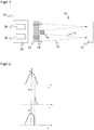
- FIG. 1 shows a schematic representation of an optoelectronic sensor 10 in an embodiment as a single-beam light scanner.
- a light transmitter 12 for example an LED or a laser light source, transmits a light signal 14 into a monitoring area 16. If it hits an object 18 there, part of the light signal is remitted or reflected and returns to a light receiver 22 as a remitted light signal 20.
- This light receiver 22 comprises a plurality of avalanche photodiode elements 24 in Geiger mode or SPADs. The received signals of the avalanche photodiode elements 24 are read out by a control and evaluation unit 26 and evaluated there.
- the control and evaluation unit 26 two blocks of the control and evaluation unit 26 are highlighted only very schematically and on a purely functional level, namely a light transit time measuring unit 28 and a control unit 30.
- the light transit time measuring unit 28 measures a light transit time from the emission of the light signal 14 to the reception of the remitted light signal 20 and converts this into a distance using the speed of light.
- the time-of-flight measuring unit 28 is not present if the sensor 10 has a task other than determining the distance using a time-of-flight method.
- the control unit 30 is able to change the sensitivity of the avalanche photodiode elements 24 in groups, as will be explained in detail further below.
- the senor 10 has further elements, in particular transmitting and receiving optics and connections, which are not discussed here for the sake of simplicity.
- the separation into light receiver 22 and control and evaluation unit 26 in Figure 1 is also conceivable in practice, but serves primarily for explanation.
- These elements are preferably at least partially integrated on a common chip, the surface of which is shared by light-sensitive areas of the avalanche photodiode elements 24 and circuits assigned to individual or groups of avalanche photodiode elements 24 for their evaluation and control.
- optical arrangement with a light transmitter 12, which covers a small portion of the light receiver 22 is purely by way of example.
- other known optical solutions can also be used, such as autocollimation with a beam splitter, for example and a common optics, or pupil division, where two separate optics are provided and the light transmitter and light receiver are arranged next to one another.
- the single-beam sensor 10 shown as a whole is also to be understood only as an example.
- An extension of the monitoring area 16 is possible by moving the beam in a laser scanner, be it with a rotating mirror or a total rotating measuring head with light transmitter 12 and / or light receiver 22.
- several single-beam systems can be combined to create a light grid with several, mostly parallel To form beams, which measures or monitors distances in each beam, in particular as a scanning light grid. It can be measured with the avalanche photodiode elements 24 individually or in groups, spatially resolved, so that a 3D camera is created.
- Mobile systems are also conceivable in which the sensor 10 is movably mounted.
- Figure 2 shows, one above the other, three representations of the time course of an accumulated received signal of the avalanche photodiode elements 24 in the region of a strong received pulse. For this purpose, the number of triggering avalanche photodiode elements 24 is plotted against time. In the upper part of the Figure 2 the entire received pulse is shown, in the middle part a remainder of the received pulse that is no longer received and in the lower part the received start area of the received pulse complementarily.
- the pulse shape is not as cleanly resolved and cut off as in the lower part of the Figure 2 so that a determination of the time of reception cannot simply be based on the maximum value that has not been shifted there. Rather, a realistic time-of-flight measurement, which for example determines the center of gravity, results in an incorrect pulse reconstruction. This leads to an error in the transit time measurement, which depends on the intensity of the received pulse and the dead time of the avalanche photodiode elements 24.
- This systematic error is a special form of the black-and-white shift or the intensity-dependent light-dark error, which has long been known for time-of-flight measurements, according to which light objects 18 are measured at a different distance than dark objects 18, now in the case of avalanche photo-diode elements 24 in Geiger mode.
- a first example according to Figure 3 two alternating groups of avalanche photo diode elements 24a-b formed, which are arranged on the light receiver 22 in a checkerboard pattern.
- the avalanche photodiode elements 24a of the first group are initially active (black) and the avalanche photodiode elements 24b of the second group are inactive (white).
- the configuration is changed with a defined time offset, now as in the right part of the Figure 3 the avalanche photodiode elements 24b of the second group are active (black) and the avalanche photodiode elements 24a of the first group are inactive (white).
- the control unit 30 can carry out this change one or more times in a regular or irregular sequence.
- the checkerboard pattern shown is just a simple example.
- the nxm avalanche photodiode elements 24 of the light receiver 22 be uniquely addressable with a pair of numbers (i, j), 1 i n, i j m.
- Now l time windows ⁇ tk, 1 k l of any length are determined, and a matrix with coefficients a k (i, j) for the sensitivity of the avalanche photo diode element 24 at position (i, j) is specified for each time window ⁇ tk.
- the coefficients a (i, j) are preferably between a minimum and maximum sensitivity and accept either only the digital values (0.1) for active and inactive or intermediate values for sensitivities in between.
- such intermediate values are preferably set by means of the value of an overvoltage above the breakdown voltage.
- the value 0 stands for below the breakdown voltage and the value 1 for a comfortable working voltage well above the breakdown voltage, the further increase of which would hardly change the sensitivity.
- the overvoltage is scaled accordingly for values between 0 and 1.
- new groups of avalanche photodiodes 24 are formed in each time window ⁇ tk, which in the extreme case each consist of only one avalanche photodiode 24.
- ⁇ tk time window
- only a few groups are preferably formed, whose group membership is retained over time, and only the sensitivity of the avalanche photodiode elements 24 of a group is changed at certain times. It is true that individual control offers the greatest flexibility, but the expense, in particular for the additional lines to each avalanche photodiode element 24, is high and reduces the fill factor. If there is a fixed group membership, however, common controls and lines can be used.
- FIG. 4 illustrates another example.
- a received pulse is shown again similar to that in FIG Figure 2 .
- the time window of the expected duration of the received pulse is subdivided, here as an example regularly and into six subsections ⁇ t1- ⁇ t6.
- a different one of six groups of avalanche photo diode elements 24 is activated, so that a population of avalanche photo diode elements 24 ready for detection is available over the entire duration of the received pulse, in which no avalanche breakdown has yet been triggered and which are not in their Dead time.
- the joint triggering with a high light load or high intensity gradients as in Figure 2 is avoided in this way.
- the electrical received pulse reconstructed from the received signal of the avalanche photodiode elements 24 does not have a shifted center of gravity; rather, its pulse shape is realistically reproduced and the black-and-white error is thus suppressed.
- Figure 5 shows a suitable possible distribution of the groups of avalanche photo diode elements 24 formed for the subsections ⁇ t1- ⁇ t6 on the light receiver 22.
- the light receiver 22 is in a regular grid of raster elements 32 divided into Figure 5 only one is exemplarily highlighted by a thick line.
- At least one avalanche photodiode element 24 of each group is provided within each raster element 32, as symbolized by numbers 1 ... 6.
- the avalanche photo diode elements 24 are thus active at number 1, and correspondingly for the further subsections ⁇ t2- ⁇ t6 the avalanche photo diode elements 24 at numbers 2 ... 6.
- the duration of the subsections ⁇ t1- ⁇ t6 is advantageously added approximately to the expected duration of the received pulse.
- the individual durations ⁇ t1- ⁇ t6 and the sequence can be uniform, but they can also be varied. A temporal overlap would also be conceivable in which at least one group is still active while the next group is already being activated.
- the control sequence is preferably repeated according to any periodic pattern in order to cover an unknown time position of the received pulse, and it can be synchronized with the transmission time of the light signal 14.
- the selected number of six subsections ⁇ t1- ⁇ t6 or six groups is only one example. However, it makes sense not to form too many groups and in particular not to form a maximum of ten groups so that a sufficient number of avalanche photodiode elements 24 is still contained in each group. Otherwise, a weaker received pulse from a distant and / or dark object 18 with too few avalanche photodiode elements 24 might no longer be detected, especially since a received light spot from the far range typically only illuminates a small part of the light receiver 22 and thus most of the avalanche photodiode elements 24 even with the highest sensitivity do not receive any useful light photons at all. A small receiving light spot from the far range can also be avoided by using homogenizing optics, such as in the DE 10 2014 102 420 A1 described, whereby as possible the entire light receiver 22 is illuminated evenly regardless of distance.
- these parameters are preferably taken into account: the photon flow, the total number of photons available avalanche photodiode elements 24, their photon detection efficiency (PDE) and their dead time.
- Figure 6 illustrates once again that not only the specifically described rasterized or checkerboard-like patterns are available for such a design, but in principle also any arrangements.
- the avalanche photodiode elements 24 active at the time under consideration are shown in black, the inactive avalanche photodiode elements 24 in white.
- such avalanche photodiode elements 24 do not have to be considered separately in that they are viewed as a further group which are set to the desired sensitivity at time zero, for example when they are switched on.
- FIG. 7 shows a basic circuit of an advantageous embodiment.
- Two avalanche photodiode elements 24a-b are connected together to form a dual avalanche photodiode 124 in such a way that the triggering of an avalanche breakdown in the one avalanche photodiode element 24a-b results in a change in sensitivity, in particular activation or deactivation, of the other avalanche photodiode element 24b- a.
- the switching elements shown are, as it were, the control unit 30 which is wholly or partially integrated into the dual avalanche photodiode 124 and which derives the point in time for a change in sensitivity dynamically from an avalanche breakdown.
- the two avalanche photodiode elements 24a-b advantageously share a charging resistor Rk.
- the two avalanche photodiode elements 24a-b are sometimes also referred to as the front avalanche photodiode element 24a and the rear avalanche photodiode element 24b. However, this is only a linguistic simplification that is based on the chronological sequence in a preferred embodiment.
- the rear avalanche photodiode element 24b can also be active first and activate the front avalanche photodiode element 24a, one avalanche photodiode element 24a-b temporarily suppressing the activity of the other avalanche photodiode element 24b-a, or both avalanche photodiode elements 24a-b are simultaneously with the same or different sensitivities active, whereby the sensitivity of the partner changes in a targeted manner after an avalanche outbreak.
- the dual avalanche photodiode 124 If the dual avalanche photodiode 124 is now illuminated, only the front avalanche photodiode element 24a, which is biased above the breakdown voltage, reacts to this, because the rear avalanche photodiode element 24b does not work in Geiger mode and is to be regarded as inactive in a relative comparison. Because of the avalanche breakdown in the front avalanche photodiode element 24a, it becomes low-resistance, and therefore the voltage drop across the rear avalanche photodiode element 24b increases, drives its bias voltage above the breakdown voltage and thus controls it in the Geiger mode or activates it.
- One avalanche photodiode element 24a-b is thus temporarily protected by the avalanche breakdown of the other avalanche photodiode element 24b-a, especially when there is strong incidence of light, so that a detectable avalanche photodiode element 24a-b then remains during the dead time.
- Figure 8 shows an exemplary, checkerboard-like arrangement of dual avalanche photo diodes 124.
- every second avalanche photo diode 124 is upside down, so to speak. Otherwise a stripe pattern would result, which is alternatively conceivable, because the respective spatial deviation by a maximum of the extent of an avalanche photo diode element 24a-b is small.
- This principle of a pattern through dual avalanche photo diodes 124 a time sequence of the activity without external control is made possible in any case, so that in particular the above-mentioned advantages of an improved reconstruction of a received pulse and ultimately the compensation of a light-dark error is achieved in a particularly simple way.
- the front avalanche photodiode elements 24a and the rear avalanche photodiode elements 24b each form one of two groups, similar to FIG Figure 3 , with the difference that in the dual avalanche photodiodes 124 the respective rear avalanche photodiodes 24b are not activated jointly as a group, but rather individually in response to an avalanche breakdown.
- Figure 9 shows an example of a parallel connection of several parallel dual avalanche photo diodes 124. If necessary, every second dual avalanche photo diode 124 can be turned upside down. In contrast to Figure 7 Here, the bias voltage is not distributed individually per dual avalanche photodiode 124 to the two respective avalanche photodiode elements 24a-b. Instead, several dual avalanche photo diodes 124 are connected in parallel, in particular all dual avalanche photo diodes 124 in a row or column, and are supplied via a common voltage divider 34.
- the voltage divider 34 can alternatively be designed in such a way that the two avalanche photo diode elements 24a-b trigger one another in reverse order, so that the dual avalanche photo diode 124 is quasi "upside down".
- dual avalanche photodiodes 124 such “upside down” and “non-upside down” dual avalanche photodiodes 124 can be mixed as desired.
- the voltage divider ratio is preferably variable in order, for example, to bias the avalanche photodiode elements 24a-b with different overvoltages and a voltage below the breakdown voltage.
- the range of variation could be 26 V ... 35 V or more.
- a variable or externally changeable setting of the voltage divider ratio is only possible for a single dual avalanche photodiode 124, even without parallel connection of a plurality of dual avalanche photodiodes 124, as in FIG Figure 7 conceivable.
- the dual avalanche photo-diodes 124 can with the use of a suitable readout circuit such as that shown in FIG EP 3 124 992B1 is presented, can also be operated at high frequencies up to the gigahertz range.
Landscapes
- Engineering & Computer Science (AREA)
- Physics & Mathematics (AREA)
- General Physics & Mathematics (AREA)
- Computer Networks & Wireless Communication (AREA)
- Radar, Positioning & Navigation (AREA)
- Remote Sensing (AREA)
- Electromagnetism (AREA)
- Spectroscopy & Molecular Physics (AREA)
- Optical Radar Systems And Details Thereof (AREA)
- Light Receiving Elements (AREA)
Claims (9)
- Récepteur de lumière (22) comprenant une pluralité d'éléments de photodiode à avalanche (24a, 24b) pouvant chacun être polarisé à une tension de polarisation supérieure à une tension de claquage et pouvant ainsi fonctionner dans un mode Geiger, dans lequel les éléments de photodiode à avalanche (24a, 24b) forment une pluralité de groupes et dans lequel deux éléments de photodiode à avalanche (24a, 24b) provenant chacun de deux groupes différents forment une photodiode à avalanche au moins double (124) avec au moins un élément de photodiode à avalanche avant (24a) et un élément de photodiode à avalanche arrière (24b), un claquage en avalanche de l'élément de photodiode à avalanche avant (24a) modifiant la sensibilité de l'élément de photodiode à avalanche arrière (24b) ou vice versa,
caractérisé en ce qu'une unité de circuit (V, R1, R2, 34) est associée à la double photodiode à avalanche (124) qui, dans un état de repos avant un claquage en avalanche, maintient l'élément de photodiode à avalanche avant (24a) à une tension de polarisation supérieure à la tension de claquage et l'élément de photodiode à avalanche arrière (24b) à une tension de polarisation inférieure à la tension de claquage ou vice versa. - Récepteur de lumière (22) selon l'une des revendications précédentes,
dans lequel une unité de mesure du temps de vol de la lumière (28) est prévue qui est configurée pour déterminer un temps de vol de la lumière d'une impulsion lumineuse à partir des signaux des éléments de photodiode à avalanche (24a, 24b). - Récepteur de lumière (22) selon l'une des revendications précédentes,
dans lequel les éléments de photodiode à avalanche (24a, 24b) forment un réseau matriciel, et dans lequel, lors d'une subdivision du réseau matriciel en une grille d'éléments de grille (32), chaque groupe comprend au moins un élément de photodiode à avalanche (24a, 24b) dans chaque élément de grille (32). - Récepteur de lumière (22) selon l'une des revendications précédentes,
dans lequel les éléments de photodiode à avalanche (24a, 24b) de deux groupes forment un motif en damier. - Récepteur de lumière (22) selon l'une des revendications précédentes,
dans lequel le claquage en avalanche de l'élément de photodiode à avalanche avant (24a) permet de modifier la polarisation de l'élément de photodiode à avalanche arrière (24b) ou vice versa. - Récepteur de lumière (22) selon l'une des revendications précédentes,
dans lequel l'unité de circuit comprend un circuit diviseur de tension (R1, R2, 34). - Récepteur de lumière (22) selon l'une des revendications précédentes,
dans lequel un circuit de retardement est prévu qui, après un claquage en avalanche dans l'élément de photodiode à avalanche avant (24a), active ou désactive l'élément de photodiode à avalanche arrière (24b) après un temps de retard pouvant être prédéterminé ou vice versa. - Capteur optoélectronique (10) avec au moins un récepteur de lumière (22) selon l'une des revendications précédentes, le capteur (10) étant en particulier un capteur de mesure de distance (10) avec un émetteur de lumière (12) pour l'émission d'un signal lumineux (14) et avec une unité de mesure du temps de vol de la lumière (28) qui est configurée pour déterminer une distance de l'objet (18) à partir d'un temps de vol de la lumière entre l'émission du signal lumineux (14) et la réception du signal lumineux (20) émis par un objet (18) d'une zone de surveillance (16).
- Procédé de détection de lumière (20) avec une pluralité d'éléments de photodiode à avalanche (24a, 24b) qui sont respectivement polarisés au moins en phase avec une tension de polarisation supérieure à une tension de claquage et qui fonctionnent ainsi dans un mode Geiger, les éléments de photodiode à avalanche (24a, 24b) formant une pluralité de groupes et la sensibilité des éléments de photodiode à avalanche (24) étant modifiée, et dans lequel deux éléments de photodiode à avalanche (24a, 24b) provenant chacun de deux groupes différents forment une photodiode à avalanche au moins double (124) ayant au moins un élément de photodiode à avalanche avant (24a) et un élément de photodiode à avalanche arrière (24b), un claquage en avalanche de l'élément de photodiode à avalanche avant (24a) modifiant la sensibilité de l'élément de photodiode à avalanche arrière (24b) ou vice versa,
caractérisé en ce qu'une unité de circuit (V, R1, R2, 34) associée à la double photodiode à avalanche (124), dans un état de repos avant un claquage en avalanche, maintient l'élément de photodiode à avalanche avant (24a) à une tension de polarisation supérieure et l'élément de photodiode à avalanche arrière (24b) à une tension de polarisation inférieure à la tension de claquage ou vice versa.
Applications Claiming Priority (1)
| Application Number | Priority Date | Filing Date | Title |
|---|---|---|---|
| DE102018120141.9A DE102018120141A1 (de) | 2018-08-17 | 2018-08-17 | Erfassen von Licht mit einer Vielzahl von Lawinenphotodiodenelementen |
Publications (2)
| Publication Number | Publication Date |
|---|---|
| EP3611535A1 EP3611535A1 (fr) | 2020-02-19 |
| EP3611535B1 true EP3611535B1 (fr) | 2021-07-14 |
Family
ID=67438152
Family Applications (1)
| Application Number | Title | Priority Date | Filing Date |
|---|---|---|---|
| EP19187266.2A Active EP3611535B1 (fr) | 2018-08-17 | 2019-07-19 | Capture de lumière à l'aide d'une pluralité d'éléments de photodiode à avalanche |
Country Status (5)
| Country | Link |
|---|---|
| US (1) | US11294037B2 (fr) |
| EP (1) | EP3611535B1 (fr) |
| JP (1) | JP6907275B2 (fr) |
| CN (1) | CN110888117B (fr) |
| DE (1) | DE102018120141A1 (fr) |
Families Citing this family (33)
| Publication number | Priority date | Publication date | Assignee | Title |
|---|---|---|---|---|
| DE102018126631A1 (de) * | 2018-10-25 | 2020-04-30 | Valeo Schalter Und Sensoren Gmbh | Verfahren zur Bestimmung einer Entfernung eines Objekts mithilfe einer optischen Detektionsvorrichtung und optische Detektionsvorrichtung |
| US11372090B2 (en) * | 2018-12-10 | 2022-06-28 | Baidu Usa Llc | Light detection and range (LIDAR) device with SPAD and APD sensors for autonomous driving vehicles |
| US11980965B2 (en) * | 2019-04-23 | 2024-05-14 | General Electric Company | Systems and methods for multi-laser head alignment in additive manufacturing systems |
| US11514594B2 (en) * | 2019-10-30 | 2022-11-29 | Vergence Automation, Inc. | Composite imaging systems using a focal plane array with in-pixel analog storage elements |
| US12144653B2 (en) | 2020-02-21 | 2024-11-19 | Hi Llc | Systems, circuits, and methods for reducing common-mode noise in biopotential recordings |
| US11950879B2 (en) | 2020-02-21 | 2024-04-09 | Hi Llc | Estimation of source-detector separation in an optical measurement system |
| US11969259B2 (en) | 2020-02-21 | 2024-04-30 | Hi Llc | Detector assemblies for a wearable module of an optical measurement system and including spring-loaded light-receiving members |
| US12029558B2 (en) | 2020-02-21 | 2024-07-09 | Hi Llc | Time domain-based optical measurement systems and methods configured to measure absolute properties of tissue |
| WO2021188485A1 (fr) | 2020-03-20 | 2021-09-23 | Hi Llc | Maintien de sensibilité de photodétecteur constante dans un système de mesure optique |
| WO2021188486A1 (fr) | 2020-03-20 | 2021-09-23 | Hi Llc | Réglage basé sur un circuit en boucle à verrouillage de phase d'une fenêtre de temps de mesure dans un système de mesure optique |
| US12059262B2 (en) | 2020-03-20 | 2024-08-13 | Hi Llc | Maintaining consistent photodetector sensitivity in an optical measurement system |
| US12085789B2 (en) | 2020-03-20 | 2024-09-10 | Hi Llc | Bias voltage generation in an optical measurement system |
| US11857348B2 (en) | 2020-03-20 | 2024-01-02 | Hi Llc | Techniques for determining a timing uncertainty of a component of an optical measurement system |
| US12138068B2 (en) | 2020-03-20 | 2024-11-12 | Hi Llc | Techniques for characterizing a nonlinearity of a time-to-digital converter in an optical measurement system |
| US20210290066A1 (en) * | 2020-03-20 | 2021-09-23 | Hi Llc | Dynamic Range Optimization in an Optical Measurement System |
| US12230649B2 (en) | 2020-05-19 | 2025-02-18 | Vergence Automation, Inc. | AI system on chip (SOC) for robotics vision applications |
| US20210389429A1 (en) * | 2020-06-15 | 2021-12-16 | Continental Automotive Systems, Inc. | Lidar system |
| US20230213627A1 (en) * | 2020-06-18 | 2023-07-06 | NewSight Imaging Ltd. | A method and active pixel array for a time of flight detection |
| TWI759213B (zh) * | 2020-07-10 | 2022-03-21 | 大陸商廣州印芯半導體技術有限公司 | 光感測器及其感測方法 |
| WO2022035626A1 (fr) | 2020-08-11 | 2022-02-17 | Hi Llc | Maintien constant de la sensibilité de photodétecteur dans un système de mesure optique |
| JP7476033B2 (ja) * | 2020-08-24 | 2024-04-30 | 株式会社東芝 | 受光装置及び電子装置 |
| JP2022039524A (ja) * | 2020-08-28 | 2022-03-10 | 株式会社東芝 | 半導体装置 |
| CN112038360A (zh) * | 2020-09-08 | 2020-12-04 | 上海大芯半导体有限公司 | 距离传感器像素阵列结构、距离传感器及工作方法 |
| CN116762021A (zh) * | 2021-02-09 | 2023-09-15 | 深圳市大疆创新科技有限公司 | 激光接收电路及其控制方法、测距装置、移动平台 |
| CN115694792B (zh) * | 2021-10-09 | 2024-07-30 | 科大国盾量子技术股份有限公司 | 可检测强脉冲光致盲攻击的方法、装置及接收端 |
| US12021107B2 (en) * | 2022-06-03 | 2024-06-25 | Lg Innotek Co., Ltd. | Systems and methods for breakdown voltage correction in Geiger-mode avalanche photodiode (APD) focal plane arrays (FPA) |
| US12225301B2 (en) * | 2022-06-06 | 2025-02-11 | Lg Innotek Co., Ltd. | Systems and methods for pixel on-off switching in focal plane arrays |
| JP2024035593A (ja) * | 2022-09-02 | 2024-03-14 | 株式会社東芝 | 光検出器及び距離計測装置 |
| CN115855245A (zh) * | 2022-11-28 | 2023-03-28 | 武汉光谷信息光电子创新中心有限公司 | 降低单光子探测器中apd间串扰的方法和单光子探测器 |
| CN118276049A (zh) * | 2022-12-29 | 2024-07-02 | 深圳市速腾聚创科技有限公司 | 一种激光探测器和激光雷达 |
| DE102023110519A1 (de) | 2023-04-25 | 2024-10-31 | Sick Ag | Optoelektronischer Sensor mit Lawinenphotodiodenelementen |
| WO2025176834A1 (fr) * | 2024-02-22 | 2025-08-28 | Voxelsensors Srl | Système de détection optique |
| EP4671816A1 (fr) * | 2024-06-27 | 2025-12-31 | VoxelSensors SRL | Système de détection optique |
Family Cites Families (14)
| Publication number | Priority date | Publication date | Assignee | Title |
|---|---|---|---|---|
| EP2708914A1 (fr) | 2012-09-18 | 2014-03-19 | Sick Ag | Capteur optoélectronique et procédé de détection d'une carte de profondeur |
| DE202013101039U1 (de) * | 2013-03-11 | 2014-03-12 | Sick Ag | Optoelektronischer Sensor zur Entfernungsmessung |
| DE102014102420A1 (de) | 2014-02-25 | 2015-08-27 | Sick Ag | Optoelektronischer Sensor und Verfahren zur Objekterfassung in einem Überwachungsbereich |
| KR102409952B1 (ko) * | 2014-04-07 | 2022-06-17 | 삼성전자주식회사 | 고해상도, 고프레임률, 저전력 이미지 센서 |
| DE102014207559A1 (de) * | 2014-04-22 | 2015-10-22 | BSH Hausgeräte GmbH | Gargerät mit Isolationskörper |
| DE102014207599B4 (de) | 2014-04-23 | 2024-09-26 | Robert Bosch Gmbh | Verfahren und Computerprogramm zum Betreiben eines Fotodetektors |
| JP6333189B2 (ja) * | 2015-02-09 | 2018-05-30 | 三菱電機株式会社 | レーザ受信装置 |
| JP6523046B2 (ja) | 2015-05-29 | 2019-05-29 | シャープ株式会社 | 光センサ |
| EP3124992B1 (fr) | 2015-07-27 | 2017-07-12 | Sick Ag | Récepteur de lumière ayant des photodiodes à avalanche en mode geiger et procédé de lecture |
| US9997551B2 (en) * | 2015-12-20 | 2018-06-12 | Apple Inc. | Spad array with pixel-level bias control |
| DE102016113131B4 (de) | 2016-07-15 | 2024-12-12 | Sick Ag | Optoelektronischer Sensor und Verfahren zur Erfassung eines Objekts in einem Überwachungsbereich |
| EP3339887B1 (fr) | 2016-12-22 | 2019-04-03 | Sick AG | Récepteur de lumière comprenant une pluralité de photodiodes à avalanche et procédé de détection de lumière |
| JP6867212B2 (ja) * | 2017-03-31 | 2021-04-28 | 株式会社デンソー | 光検出器及び測距装置 |
| JP6932580B2 (ja) * | 2017-08-04 | 2021-09-08 | ソニーセミコンダクタソリューションズ株式会社 | 固体撮像素子 |
-
2018
- 2018-08-17 DE DE102018120141.9A patent/DE102018120141A1/de not_active Withdrawn
-
2019
- 2019-07-19 EP EP19187266.2A patent/EP3611535B1/fr active Active
- 2019-08-08 US US16/535,426 patent/US11294037B2/en active Active
- 2019-08-15 JP JP2019149043A patent/JP6907275B2/ja active Active
- 2019-08-16 CN CN201910760185.9A patent/CN110888117B/zh active Active
Non-Patent Citations (1)
| Title |
|---|
| None * |
Also Published As
| Publication number | Publication date |
|---|---|
| EP3611535A1 (fr) | 2020-02-19 |
| CN110888117B (zh) | 2022-11-15 |
| US11294037B2 (en) | 2022-04-05 |
| CN110888117A (zh) | 2020-03-17 |
| US20200057146A1 (en) | 2020-02-20 |
| JP2020042021A (ja) | 2020-03-19 |
| DE102018120141A1 (de) | 2020-02-20 |
| JP6907275B2 (ja) | 2021-07-21 |
Similar Documents
| Publication | Publication Date | Title |
|---|---|---|
| EP3611535B1 (fr) | Capture de lumière à l'aide d'une pluralité d'éléments de photodiode à avalanche | |
| DE102017113675B4 (de) | Optoelektronischer Sensor und Verfahren zur Messung der Entfernung zu einem Objekt | |
| DE102017101501B3 (de) | Optoelektronischer Sensor und Verfahren zur Bestimmung der Entfernung eines Objekts in einem Überwachungsbereich | |
| DE102014207599B4 (de) | Verfahren und Computerprogramm zum Betreiben eines Fotodetektors | |
| EP3418766B1 (fr) | Capteur optoélectronique et procédé de mesure de la distance par rapport à un objet | |
| EP3130889B1 (fr) | Télémètre optique | |
| EP1884797B1 (fr) | Dispositif et procédé destinés à la détermination de distance | |
| DE112020001783T5 (de) | Flugzeitsensor | |
| EP3557286B1 (fr) | Capteur optoélectronique et procédé de détection et de détermination de distance d'un objet | |
| EP3557284A2 (fr) | Capteur optoélectronique et procédé de détermination de la distance | |
| EP3985412B1 (fr) | Mesure de distance selon un procédé de temps de propagation de la lumière | |
| DE102017222971A1 (de) | LIDAR Empfangseinheit | |
| EP3724685B1 (fr) | Procédé de détection rapprochée et à distance améliorée d'une unité de réception lidar | |
| DE102011005740A1 (de) | Messvorrichtung zur Messung einer Entfernung zwischen der Messvorrichtung und einem Zielobjekt mit Hilfe optischer Messstrahlung | |
| DE202013105389U1 (de) | Optoelektronischer Sensor mit im Geiger-Modus betriebenen Lawinenphotodiodenelementen | |
| WO2020114740A1 (fr) | Système lidar et véhicule à moteur | |
| EP3775982A1 (fr) | Procédé pour realiser un processus de mesure | |
| DE102016113131B4 (de) | Optoelektronischer Sensor und Verfahren zur Erfassung eines Objekts in einem Überwachungsbereich | |
| EP4249950B1 (fr) | Détection et détermination de la distance d'un objet | |
| EP3355078A1 (fr) | Capteur optoélectronique et procédé de détection d'objets | |
| EP3650888B1 (fr) | Détecteur optoélectronique et procédé de détection et de détermination de distance des objets | |
| EP4045931A1 (fr) | Système lidar à impulsions multiples et procédé de capture d'un objet dans une région observée | |
| EP4455720B1 (fr) | Capteur optoélectronique avec éléments photodiodes à avalanche | |
| EP3910373B1 (fr) | Lecture des éléments photodiodes d'avalanche en mode geiger | |
| EP4249949A1 (fr) | Détection et détermination de la distance d'un objet |
Legal Events
| Date | Code | Title | Description |
|---|---|---|---|
| PUAI | Public reference made under article 153(3) epc to a published international application that has entered the european phase |
Free format text: ORIGINAL CODE: 0009012 |
|
| STAA | Information on the status of an ep patent application or granted ep patent |
Free format text: STATUS: THE APPLICATION HAS BEEN PUBLISHED |
|
| AK | Designated contracting states |
Kind code of ref document: A1 Designated state(s): AL AT BE BG CH CY CZ DE DK EE ES FI FR GB GR HR HU IE IS IT LI LT LU LV MC MK MT NL NO PL PT RO RS SE SI SK SM TR |
|
| AX | Request for extension of the european patent |
Extension state: BA ME |
|
| STAA | Information on the status of an ep patent application or granted ep patent |
Free format text: STATUS: REQUEST FOR EXAMINATION WAS MADE |
|
| 17P | Request for examination filed |
Effective date: 20200317 |
|
| RBV | Designated contracting states (corrected) |
Designated state(s): AL AT BE BG CH CY CZ DE DK EE ES FI FR GB GR HR HU IE IS IT LI LT LU LV MC MK MT NL NO PL PT RO RS SE SI SK SM TR |
|
| STAA | Information on the status of an ep patent application or granted ep patent |
Free format text: STATUS: EXAMINATION IS IN PROGRESS |
|
| 17Q | First examination report despatched |
Effective date: 20200720 |
|
| GRAP | Despatch of communication of intention to grant a patent |
Free format text: ORIGINAL CODE: EPIDOSNIGR1 |
|
| STAA | Information on the status of an ep patent application or granted ep patent |
Free format text: STATUS: GRANT OF PATENT IS INTENDED |
|
| RIC1 | Information provided on ipc code assigned before grant |
Ipc: G01S 7/4863 20200101AFI20210317BHEP Ipc: G01S 7/4865 20200101ALI20210317BHEP Ipc: G01S 7/487 20060101ALI20210317BHEP Ipc: G01S 7/497 20060101ALI20210317BHEP Ipc: G01S 17/10 20200101ALI20210317BHEP Ipc: G01S 17/894 20200101ALI20210317BHEP Ipc: G01J 1/44 20060101ALI20210317BHEP Ipc: H01L 31/02 20060101ALI20210317BHEP Ipc: G01S 17/18 20200101ALN20210317BHEP Ipc: G01S 17/42 20060101ALN20210317BHEP |
|
| INTG | Intention to grant announced |
Effective date: 20210409 |
|
| GRAS | Grant fee paid |
Free format text: ORIGINAL CODE: EPIDOSNIGR3 |
|
| GRAA | (expected) grant |
Free format text: ORIGINAL CODE: 0009210 |
|
| STAA | Information on the status of an ep patent application or granted ep patent |
Free format text: STATUS: THE PATENT HAS BEEN GRANTED |
|
| AK | Designated contracting states |
Kind code of ref document: B1 Designated state(s): AL AT BE BG CH CY CZ DE DK EE ES FI FR GB GR HR HU IE IS IT LI LT LU LV MC MK MT NL NO PL PT RO RS SE SI SK SM TR |
|
| REG | Reference to a national code |
Ref country code: GB Ref legal event code: FG4D Free format text: NOT ENGLISH |
|
| REG | Reference to a national code |
Ref country code: DE Ref legal event code: R096 Ref document number: 502019001805 Country of ref document: DE |
|
| REG | Reference to a national code |
Ref country code: IE Ref legal event code: FG4D Free format text: LANGUAGE OF EP DOCUMENT: GERMAN |
|
| REG | Reference to a national code |
Ref country code: AT Ref legal event code: REF Ref document number: 1411096 Country of ref document: AT Kind code of ref document: T Effective date: 20210815 |
|
| REG | Reference to a national code |
Ref country code: LT Ref legal event code: MG9D |
|
| REG | Reference to a national code |
Ref country code: NL Ref legal event code: MP Effective date: 20210714 |
|
| PG25 | Lapsed in a contracting state [announced via postgrant information from national office to epo] |
Ref country code: HR Free format text: LAPSE BECAUSE OF FAILURE TO SUBMIT A TRANSLATION OF THE DESCRIPTION OR TO PAY THE FEE WITHIN THE PRESCRIBED TIME-LIMIT Effective date: 20210714 Ref country code: NO Free format text: LAPSE BECAUSE OF FAILURE TO SUBMIT A TRANSLATION OF THE DESCRIPTION OR TO PAY THE FEE WITHIN THE PRESCRIBED TIME-LIMIT Effective date: 20211014 Ref country code: NL Free format text: LAPSE BECAUSE OF FAILURE TO SUBMIT A TRANSLATION OF THE DESCRIPTION OR TO PAY THE FEE WITHIN THE PRESCRIBED TIME-LIMIT Effective date: 20210714 Ref country code: PT Free format text: LAPSE BECAUSE OF FAILURE TO SUBMIT A TRANSLATION OF THE DESCRIPTION OR TO PAY THE FEE WITHIN THE PRESCRIBED TIME-LIMIT Effective date: 20211115 Ref country code: LT Free format text: LAPSE BECAUSE OF FAILURE TO SUBMIT A TRANSLATION OF THE DESCRIPTION OR TO PAY THE FEE WITHIN THE PRESCRIBED TIME-LIMIT Effective date: 20210714 Ref country code: BG Free format text: LAPSE BECAUSE OF FAILURE TO SUBMIT A TRANSLATION OF THE DESCRIPTION OR TO PAY THE FEE WITHIN THE PRESCRIBED TIME-LIMIT Effective date: 20211014 Ref country code: SE Free format text: LAPSE BECAUSE OF FAILURE TO SUBMIT A TRANSLATION OF THE DESCRIPTION OR TO PAY THE FEE WITHIN THE PRESCRIBED TIME-LIMIT Effective date: 20210714 Ref country code: RS Free format text: LAPSE BECAUSE OF FAILURE TO SUBMIT A TRANSLATION OF THE DESCRIPTION OR TO PAY THE FEE WITHIN THE PRESCRIBED TIME-LIMIT Effective date: 20210714 Ref country code: FI Free format text: LAPSE BECAUSE OF FAILURE TO SUBMIT A TRANSLATION OF THE DESCRIPTION OR TO PAY THE FEE WITHIN THE PRESCRIBED TIME-LIMIT Effective date: 20210714 Ref country code: ES Free format text: LAPSE BECAUSE OF FAILURE TO SUBMIT A TRANSLATION OF THE DESCRIPTION OR TO PAY THE FEE WITHIN THE PRESCRIBED TIME-LIMIT Effective date: 20210714 |
|
| PG25 | Lapsed in a contracting state [announced via postgrant information from national office to epo] |
Ref country code: PL Free format text: LAPSE BECAUSE OF FAILURE TO SUBMIT A TRANSLATION OF THE DESCRIPTION OR TO PAY THE FEE WITHIN THE PRESCRIBED TIME-LIMIT Effective date: 20210714 Ref country code: LV Free format text: LAPSE BECAUSE OF FAILURE TO SUBMIT A TRANSLATION OF THE DESCRIPTION OR TO PAY THE FEE WITHIN THE PRESCRIBED TIME-LIMIT Effective date: 20210714 Ref country code: GR Free format text: LAPSE BECAUSE OF FAILURE TO SUBMIT A TRANSLATION OF THE DESCRIPTION OR TO PAY THE FEE WITHIN THE PRESCRIBED TIME-LIMIT Effective date: 20211015 |
|
| REG | Reference to a national code |
Ref country code: BE Ref legal event code: MM Effective date: 20210731 |
|
| REG | Reference to a national code |
Ref country code: DE Ref legal event code: R097 Ref document number: 502019001805 Country of ref document: DE |
|
| PG25 | Lapsed in a contracting state [announced via postgrant information from national office to epo] |
Ref country code: DK Free format text: LAPSE BECAUSE OF FAILURE TO SUBMIT A TRANSLATION OF THE DESCRIPTION OR TO PAY THE FEE WITHIN THE PRESCRIBED TIME-LIMIT Effective date: 20210714 |
|
| PLBE | No opposition filed within time limit |
Free format text: ORIGINAL CODE: 0009261 |
|
| STAA | Information on the status of an ep patent application or granted ep patent |
Free format text: STATUS: NO OPPOSITION FILED WITHIN TIME LIMIT |
|
| PG25 | Lapsed in a contracting state [announced via postgrant information from national office to epo] |
Ref country code: SM Free format text: LAPSE BECAUSE OF FAILURE TO SUBMIT A TRANSLATION OF THE DESCRIPTION OR TO PAY THE FEE WITHIN THE PRESCRIBED TIME-LIMIT Effective date: 20210714 Ref country code: SK Free format text: LAPSE BECAUSE OF FAILURE TO SUBMIT A TRANSLATION OF THE DESCRIPTION OR TO PAY THE FEE WITHIN THE PRESCRIBED TIME-LIMIT Effective date: 20210714 Ref country code: RO Free format text: LAPSE BECAUSE OF FAILURE TO SUBMIT A TRANSLATION OF THE DESCRIPTION OR TO PAY THE FEE WITHIN THE PRESCRIBED TIME-LIMIT Effective date: 20210714 Ref country code: MC Free format text: LAPSE BECAUSE OF FAILURE TO SUBMIT A TRANSLATION OF THE DESCRIPTION OR TO PAY THE FEE WITHIN THE PRESCRIBED TIME-LIMIT Effective date: 20210714 Ref country code: LU Free format text: LAPSE BECAUSE OF NON-PAYMENT OF DUE FEES Effective date: 20210719 Ref country code: EE Free format text: LAPSE BECAUSE OF FAILURE TO SUBMIT A TRANSLATION OF THE DESCRIPTION OR TO PAY THE FEE WITHIN THE PRESCRIBED TIME-LIMIT Effective date: 20210714 Ref country code: CZ Free format text: LAPSE BECAUSE OF FAILURE TO SUBMIT A TRANSLATION OF THE DESCRIPTION OR TO PAY THE FEE WITHIN THE PRESCRIBED TIME-LIMIT Effective date: 20210714 Ref country code: AL Free format text: LAPSE BECAUSE OF FAILURE TO SUBMIT A TRANSLATION OF THE DESCRIPTION OR TO PAY THE FEE WITHIN THE PRESCRIBED TIME-LIMIT Effective date: 20210714 |
|
| 26N | No opposition filed |
Effective date: 20220419 |
|
| PG25 | Lapsed in a contracting state [announced via postgrant information from national office to epo] |
Ref country code: IT Free format text: LAPSE BECAUSE OF FAILURE TO SUBMIT A TRANSLATION OF THE DESCRIPTION OR TO PAY THE FEE WITHIN THE PRESCRIBED TIME-LIMIT Effective date: 20210714 Ref country code: IE Free format text: LAPSE BECAUSE OF NON-PAYMENT OF DUE FEES Effective date: 20210719 Ref country code: FR Free format text: LAPSE BECAUSE OF NON-PAYMENT OF DUE FEES Effective date: 20210914 Ref country code: BE Free format text: LAPSE BECAUSE OF NON-PAYMENT OF DUE FEES Effective date: 20210731 |
|
| PG25 | Lapsed in a contracting state [announced via postgrant information from national office to epo] |
Ref country code: CY Free format text: LAPSE BECAUSE OF FAILURE TO SUBMIT A TRANSLATION OF THE DESCRIPTION OR TO PAY THE FEE WITHIN THE PRESCRIBED TIME-LIMIT Effective date: 20210714 |
|
| PG25 | Lapsed in a contracting state [announced via postgrant information from national office to epo] |
Ref country code: HU Free format text: LAPSE BECAUSE OF FAILURE TO SUBMIT A TRANSLATION OF THE DESCRIPTION OR TO PAY THE FEE WITHIN THE PRESCRIBED TIME-LIMIT; INVALID AB INITIO Effective date: 20190719 |
|
| GBPC | Gb: european patent ceased through non-payment of renewal fee |
Effective date: 20230719 |
|
| PG25 | Lapsed in a contracting state [announced via postgrant information from national office to epo] |
Ref country code: MK Free format text: LAPSE BECAUSE OF FAILURE TO SUBMIT A TRANSLATION OF THE DESCRIPTION OR TO PAY THE FEE WITHIN THE PRESCRIBED TIME-LIMIT Effective date: 20210714 Ref country code: GB Free format text: LAPSE BECAUSE OF NON-PAYMENT OF DUE FEES Effective date: 20230719 |
|
| PG25 | Lapsed in a contracting state [announced via postgrant information from national office to epo] |
Ref country code: MT Free format text: LAPSE BECAUSE OF FAILURE TO SUBMIT A TRANSLATION OF THE DESCRIPTION OR TO PAY THE FEE WITHIN THE PRESCRIBED TIME-LIMIT Effective date: 20210714 |
|
| PGFP | Annual fee paid to national office [announced via postgrant information from national office to epo] |
Ref country code: DE Payment date: 20250722 Year of fee payment: 7 |
|
| PGFP | Annual fee paid to national office [announced via postgrant information from national office to epo] |
Ref country code: AT Payment date: 20250721 Year of fee payment: 7 |
|
| PGFP | Annual fee paid to national office [announced via postgrant information from national office to epo] |
Ref country code: CH Payment date: 20250801 Year of fee payment: 7 |
|
| PG25 | Lapsed in a contracting state [announced via postgrant information from national office to epo] |
Ref country code: TR Free format text: LAPSE BECAUSE OF FAILURE TO SUBMIT A TRANSLATION OF THE DESCRIPTION OR TO PAY THE FEE WITHIN THE PRESCRIBED TIME-LIMIT Effective date: 20210714 |