EP3340318A1 - Fotovoltaik-vorrichtung und entsprechendes herstellungsverfahren - Google Patents
Fotovoltaik-vorrichtung und entsprechendes herstellungsverfahren Download PDFInfo
- Publication number
- EP3340318A1 EP3340318A1 EP17209141.5A EP17209141A EP3340318A1 EP 3340318 A1 EP3340318 A1 EP 3340318A1 EP 17209141 A EP17209141 A EP 17209141A EP 3340318 A1 EP3340318 A1 EP 3340318A1
- Authority
- EP
- European Patent Office
- Prior art keywords
- photovoltaic
- electrical contact
- region
- contact section
- collector
- Prior art date
- Legal status (The legal status is an assumption and is not a legal conclusion. Google has not performed a legal analysis and makes no representation as to the accuracy of the status listed.)
- Withdrawn
Links
- 238000004519 manufacturing process Methods 0.000 title claims description 6
- 239000000758 substrate Substances 0.000 claims abstract description 46
- 229910052751 metal Inorganic materials 0.000 claims description 55
- 239000002184 metal Substances 0.000 claims description 55
- 238000000034 method Methods 0.000 claims description 32
- 229910021417 amorphous silicon Inorganic materials 0.000 claims description 22
- 238000002161 passivation Methods 0.000 claims description 22
- 239000000463 material Substances 0.000 claims description 13
- XLOMVQKBTHCTTD-UHFFFAOYSA-N Zinc monoxide Chemical compound [Zn]=O XLOMVQKBTHCTTD-UHFFFAOYSA-N 0.000 claims description 10
- ZOXJGFHDIHLPTG-UHFFFAOYSA-N Boron Chemical compound [B] ZOXJGFHDIHLPTG-UHFFFAOYSA-N 0.000 claims description 7
- 229910052796 boron Inorganic materials 0.000 claims description 7
- 229910052738 indium Inorganic materials 0.000 claims description 6
- APFVFJFRJDLVQX-UHFFFAOYSA-N indium atom Chemical compound [In] APFVFJFRJDLVQX-UHFFFAOYSA-N 0.000 claims description 6
- 229910052684 Cerium Inorganic materials 0.000 claims description 5
- 229910052782 aluminium Inorganic materials 0.000 claims description 5
- XAGFODPZIPBFFR-UHFFFAOYSA-N aluminium Chemical compound [Al] XAGFODPZIPBFFR-UHFFFAOYSA-N 0.000 claims description 5
- 229910052793 cadmium Inorganic materials 0.000 claims description 5
- BDOSMKKIYDKNTQ-UHFFFAOYSA-N cadmium atom Chemical compound [Cd] BDOSMKKIYDKNTQ-UHFFFAOYSA-N 0.000 claims description 5
- GWXLDORMOJMVQZ-UHFFFAOYSA-N cerium Chemical compound [Ce] GWXLDORMOJMVQZ-UHFFFAOYSA-N 0.000 claims description 5
- 229910052739 hydrogen Inorganic materials 0.000 claims description 5
- 239000001257 hydrogen Substances 0.000 claims description 5
- 125000004435 hydrogen atom Chemical class [H]* 0.000 claims description 5
- 229910003437 indium oxide Inorganic materials 0.000 claims description 5
- PJXISJQVUVHSOJ-UHFFFAOYSA-N indium(iii) oxide Chemical compound [O-2].[O-2].[O-2].[In+3].[In+3] PJXISJQVUVHSOJ-UHFFFAOYSA-N 0.000 claims description 5
- WFKWXMTUELFFGS-UHFFFAOYSA-N tungsten Chemical compound [W] WFKWXMTUELFFGS-UHFFFAOYSA-N 0.000 claims description 5
- 229910052721 tungsten Inorganic materials 0.000 claims description 5
- 239000010937 tungsten Substances 0.000 claims description 5
- 239000011787 zinc oxide Substances 0.000 claims description 5
- ATJFFYVFTNAWJD-UHFFFAOYSA-N Tin Chemical compound [Sn] ATJFFYVFTNAWJD-UHFFFAOYSA-N 0.000 claims description 4
- 229910052718 tin Inorganic materials 0.000 claims description 4
- 239000011135 tin Substances 0.000 claims description 4
- 238000005234 chemical deposition Methods 0.000 claims description 2
- 239000012808 vapor phase Substances 0.000 claims description 2
- 150000002500 ions Chemical class 0.000 claims 1
- 238000000623 plasma-assisted chemical vapour deposition Methods 0.000 description 9
- 238000000151 deposition Methods 0.000 description 5
- 238000007650 screen-printing Methods 0.000 description 5
- 239000011159 matrix material Substances 0.000 description 4
- 230000015572 biosynthetic process Effects 0.000 description 3
- 239000004020 conductor Substances 0.000 description 3
- 238000005520 cutting process Methods 0.000 description 3
- 230000000873 masking effect Effects 0.000 description 3
- 238000000206 photolithography Methods 0.000 description 3
- OAICVXFJPJFONN-UHFFFAOYSA-N Phosphorus Chemical compound [P] OAICVXFJPJFONN-UHFFFAOYSA-N 0.000 description 2
- XUIMIQQOPSSXEZ-UHFFFAOYSA-N Silicon Chemical compound [Si] XUIMIQQOPSSXEZ-UHFFFAOYSA-N 0.000 description 2
- 229910052785 arsenic Inorganic materials 0.000 description 2
- RQNWIZPPADIBDY-UHFFFAOYSA-N arsenic atom Chemical compound [As] RQNWIZPPADIBDY-UHFFFAOYSA-N 0.000 description 2
- 230000007547 defect Effects 0.000 description 2
- 230000008021 deposition Effects 0.000 description 2
- 239000002019 doping agent Substances 0.000 description 2
- 239000011521 glass Substances 0.000 description 2
- 238000002955 isolation Methods 0.000 description 2
- 229910021421 monocrystalline silicon Inorganic materials 0.000 description 2
- 229910052698 phosphorus Inorganic materials 0.000 description 2
- 239000011574 phosphorus Substances 0.000 description 2
- 238000007639 printing Methods 0.000 description 2
- 230000002829 reductive effect Effects 0.000 description 2
- 229910052710 silicon Inorganic materials 0.000 description 2
- 239000010703 silicon Substances 0.000 description 2
- 229910052709 silver Inorganic materials 0.000 description 2
- 239000004332 silver Substances 0.000 description 2
- 239000000126 substance Substances 0.000 description 2
- JBRZTFJDHDCESZ-UHFFFAOYSA-N AsGa Chemical compound [As]#[Ga] JBRZTFJDHDCESZ-UHFFFAOYSA-N 0.000 description 1
- 239000005046 Chlorosilane Substances 0.000 description 1
- RYGMFSIKBFXOCR-UHFFFAOYSA-N Copper Chemical compound [Cu] RYGMFSIKBFXOCR-UHFFFAOYSA-N 0.000 description 1
- 229910001218 Gallium arsenide Inorganic materials 0.000 description 1
- BLRPTPMANUNPDV-UHFFFAOYSA-N Silane Chemical compound [SiH4] BLRPTPMANUNPDV-UHFFFAOYSA-N 0.000 description 1
- BQCADISMDOOEFD-UHFFFAOYSA-N Silver Chemical compound [Ag] BQCADISMDOOEFD-UHFFFAOYSA-N 0.000 description 1
- 238000006243 chemical reaction Methods 0.000 description 1
- KOPOQZFJUQMUML-UHFFFAOYSA-N chlorosilane Chemical compound Cl[SiH3] KOPOQZFJUQMUML-UHFFFAOYSA-N 0.000 description 1
- 229910052802 copper Inorganic materials 0.000 description 1
- 239000010949 copper Substances 0.000 description 1
- 229910021419 crystalline silicon Inorganic materials 0.000 description 1
- 229910052732 germanium Inorganic materials 0.000 description 1
- GNPVGFCGXDBREM-UHFFFAOYSA-N germanium atom Chemical compound [Ge] GNPVGFCGXDBREM-UHFFFAOYSA-N 0.000 description 1
- 239000003292 glue Substances 0.000 description 1
- 230000000670 limiting effect Effects 0.000 description 1
- 239000000203 mixture Substances 0.000 description 1
- 230000036961 partial effect Effects 0.000 description 1
- 238000005289 physical deposition Methods 0.000 description 1
- 229910021420 polycrystalline silicon Inorganic materials 0.000 description 1
- 229920000642 polymer Polymers 0.000 description 1
- 239000002861 polymer material Substances 0.000 description 1
- 239000002243 precursor Substances 0.000 description 1
- 230000000284 resting effect Effects 0.000 description 1
- 229910000077 silane Inorganic materials 0.000 description 1
- 238000007740 vapor deposition Methods 0.000 description 1
Images


Classifications
-
- H—ELECTRICITY
- H10—SEMICONDUCTOR DEVICES; ELECTRIC SOLID-STATE DEVICES NOT OTHERWISE PROVIDED FOR
- H10F—INORGANIC SEMICONDUCTOR DEVICES SENSITIVE TO INFRARED RADIATION, LIGHT, ELECTROMAGNETIC RADIATION OF SHORTER WAVELENGTH OR CORPUSCULAR RADIATION
- H10F10/00—Individual photovoltaic cells, e.g. solar cells
- H10F10/10—Individual photovoltaic cells, e.g. solar cells having potential barriers
- H10F10/16—Photovoltaic cells having only PN heterojunction potential barriers
- H10F10/164—Photovoltaic cells having only PN heterojunction potential barriers comprising heterojunctions with Group IV materials, e.g. ITO/Si or GaAs/SiGe photovoltaic cells
- H10F10/165—Photovoltaic cells having only PN heterojunction potential barriers comprising heterojunctions with Group IV materials, e.g. ITO/Si or GaAs/SiGe photovoltaic cells the heterojunctions being Group IV-IV heterojunctions, e.g. Si/Ge, SiGe/Si or Si/SiC photovoltaic cells
- H10F10/166—Photovoltaic cells having only PN heterojunction potential barriers comprising heterojunctions with Group IV materials, e.g. ITO/Si or GaAs/SiGe photovoltaic cells the heterojunctions being Group IV-IV heterojunctions, e.g. Si/Ge, SiGe/Si or Si/SiC photovoltaic cells the Group IV-IV heterojunctions being heterojunctions of crystalline and amorphous materials, e.g. silicon heterojunction [SHJ] photovoltaic cells
-
- H—ELECTRICITY
- H10—SEMICONDUCTOR DEVICES; ELECTRIC SOLID-STATE DEVICES NOT OTHERWISE PROVIDED FOR
- H10F—INORGANIC SEMICONDUCTOR DEVICES SENSITIVE TO INFRARED RADIATION, LIGHT, ELECTROMAGNETIC RADIATION OF SHORTER WAVELENGTH OR CORPUSCULAR RADIATION
- H10F19/00—Integrated devices, or assemblies of multiple devices, comprising at least one photovoltaic cell covered by group H10F10/00, e.g. photovoltaic modules
- H10F19/20—Integrated devices, or assemblies of multiple devices, comprising at least one photovoltaic cell covered by group H10F10/00, e.g. photovoltaic modules comprising photovoltaic cells in arrays in or on a single semiconductor substrate, the photovoltaic cells having planar junctions
-
- H—ELECTRICITY
- H10—SEMICONDUCTOR DEVICES; ELECTRIC SOLID-STATE DEVICES NOT OTHERWISE PROVIDED FOR
- H10F—INORGANIC SEMICONDUCTOR DEVICES SENSITIVE TO INFRARED RADIATION, LIGHT, ELECTROMAGNETIC RADIATION OF SHORTER WAVELENGTH OR CORPUSCULAR RADIATION
- H10F71/00—Manufacture or treatment of devices covered by this subclass
- H10F71/121—The active layers comprising only Group IV materials
-
- Y—GENERAL TAGGING OF NEW TECHNOLOGICAL DEVELOPMENTS; GENERAL TAGGING OF CROSS-SECTIONAL TECHNOLOGIES SPANNING OVER SEVERAL SECTIONS OF THE IPC; TECHNICAL SUBJECTS COVERED BY FORMER USPC CROSS-REFERENCE ART COLLECTIONS [XRACs] AND DIGESTS
- Y02—TECHNOLOGIES OR APPLICATIONS FOR MITIGATION OR ADAPTATION AGAINST CLIMATE CHANGE
- Y02E—REDUCTION OF GREENHOUSE GAS [GHG] EMISSIONS, RELATED TO ENERGY GENERATION, TRANSMISSION OR DISTRIBUTION
- Y02E10/00—Energy generation through renewable energy sources
- Y02E10/50—Photovoltaic [PV] energy
- Y02E10/547—Monocrystalline silicon PV cells
-
- Y—GENERAL TAGGING OF NEW TECHNOLOGICAL DEVELOPMENTS; GENERAL TAGGING OF CROSS-SECTIONAL TECHNOLOGIES SPANNING OVER SEVERAL SECTIONS OF THE IPC; TECHNICAL SUBJECTS COVERED BY FORMER USPC CROSS-REFERENCE ART COLLECTIONS [XRACs] AND DIGESTS
- Y02—TECHNOLOGIES OR APPLICATIONS FOR MITIGATION OR ADAPTATION AGAINST CLIMATE CHANGE
- Y02P—CLIMATE CHANGE MITIGATION TECHNOLOGIES IN THE PRODUCTION OR PROCESSING OF GOODS
- Y02P70/00—Climate change mitigation technologies in the production process for final industrial or consumer products
- Y02P70/50—Manufacturing or production processes characterised by the final manufactured product
Definitions
- the present invention relates to a photovoltaic device comprising at least a first heterojunction photovoltaic cell and at least one second heterojunction photovoltaic cell formed on a support substrate.
- a photovoltaic panel 10 presented to the figure 1 comprises, in general, a plurality of rows 20 of photovoltaic cells 30, each extending in a direction of elongation E, and parallel to each other.
- the set of photovoltaic cells 30 are connected in series by means of conducting ribbons 40 each connecting the front face 31 of a photovoltaic cell with the rear face 32 of another photovoltaic cell which is adjacent to it.
- a spacing Es typically between 3 and 4 mm, between the photovoltaic cells 30 allows the passage of the conductive strips 40.
- the passage of the conductive strips 40 at the spacings Es between the photovoltaic cells 30 is the main source of failures. More particularly, and as shown on the figure 2 , the conductive ribbons 40 have an embrittlement zone F, induced by their deformation at the Es spacings, which is liable to break under the repeated action of stresses, in particular the stresses induced by the exposure of the photovoltaic panels to large variations temperature.
- spacings Es between photovoltaic cells 30 do not participate in the conversion of light into electrical voltage. These spacings Es, also called “white areas”, thus reduce the efficiency of the photovoltaic panel 10.
- the introduction of the conductive strips 40 during the assembly of the photovoltaic cells 30 on a photovoltaic panel 10 imposes steps of manipulation of said photovoltaic cells 30 which are a source of defectivity directly affecting the performance of the photovoltaic panel 10.
- photovoltaic cells 30 of smaller size provides a number of advantages, among which is the reduction of the current and consequently the reduction of the ohmic losses, but also the possibility of increasing the electrical voltage delivered by a photovoltaic panel. 10 without increasing the size.
- An object of the present invention is then to provide a photovoltaic device comprising photovoltaic cells, and to improve the reliability of photovoltaic panels.
- Another object of the invention is to provide a photovoltaic device comprising photovoltaic cells for simplifying the assembly of said panels.
- Another object of the invention is also to provide a photovoltaic device for improving the efficiency of photovoltaic panels.
- Another object of the invention is to propose a photovoltaic device making it possible to consider smaller photovoltaic cells without complicating the assembly process of the photovoltaic panels.
- first photovoltaic cell and the second photovoltaic cell of a photovoltaic element are electrically connected in series.
- Front face comprises the face of the device for receiving the main sun.
- the arrangement of the at least one first photovoltaic cell and the at least one second photovoltaic cell makes it possible to dispense with conductive ribbons connecting a front face of a cell with a rear face of another cell, and reliability issues associated with them.
- the photovoltaic device according to the invention does not require isolation means to electrically isolate the at least one first photovoltaic cell from the at least one second photovoltaic cell.
- the device comprises a plurality of photovoltaic elements electrically connected in series by at least one rear electrical contact, each rear electrical contact electrically connecting the first collector region of a photovoltaic element, said first photovoltaic element, to the second emitting region of another photovoltaic element immediately adjacent to the first photovoltaic element.
- the rear electrical contact comprises a first rear electrical contact section and a second rear electrical contact section, in contact, respectively, with the first collector region of a photovoltaic element, said first photovoltaic element, at the second emitting region of another photovoltaic element immediately adjacent to the first photovoltaic element, each rear electrical contact also comprises a rear metal contact section which connects the first rear electrical contact section and the second rear electrical contact section of said electrical contact.
- the rear metal contact section comprises rear metal fingers.
- the first rear electrical contact section and the second rear electrical contact section are formed by a transparent conductive oxide layer, advantageously the transparent conductive oxide comprises at least one of the materials selected from : indium oxide advantageously comprising at least one of the elements selected from: tin, hydrogen, tungsten, cerium, cadmium; or zinc oxide comprising at least one of the elements selected from: aluminum, indium, boron.
- the transparent conductive oxide comprises at least one of the materials selected from : indium oxide advantageously comprising at least one of the elements selected from: tin, hydrogen, tungsten, cerium, cadmium; or zinc oxide comprising at least one of the elements selected from: aluminum, indium, boron.
- the front electrical contact comprises a first front electrical contact section and a second front electrical contact section, in contact, respectively, with the first emitter region, and the second collector region of a photovoltaic element.
- the front electrical contact further comprises a front metal contact section which connects the first electrical contact section and the second electrical contact section of said contact front electric, advantageously the front metal contact section comprises front metal fingers.
- the first front electrical contact section and the second front electrical contact section are formed by a transparent conductive oxide layer, advantageously the transparent conductive oxide comprises at least one of the materials selected from : indium oxide advantageously comprising at least one of the elements selected from: tin, hydrogen, tungsten, cerium, cadmium; or zinc oxide comprising at least one of the elements selected from: aluminum, indium, boron.
- the transparent conductive oxide comprises at least one of the materials selected from : indium oxide advantageously comprising at least one of the elements selected from: tin, hydrogen, tungsten, cerium, cadmium; or zinc oxide comprising at least one of the elements selected from: aluminum, indium, boron.
- the support substrate is completely covered with a passivation layer so that the first emitting and collecting regions and the second emitting and collecting regions rest on said passivation layer.
- the passivation layer comprises amorphous silicon, preferably amorphous silicon comprises a doping level less than 10 20 at / cm 3, still more preferably amorphous silicon is intrinsic.
- the first emitter region and the second collector region of the photovoltaic element are spaced a distance a1 of less than 2 mm, advantageously a zero distance.
- the first collector region and the second emitter region of the photovoltaic element are spaced a distance a2 of less than 2 mm, advantageously of a distance equal to 1 mm.
- first front electrical contact section and the second front electrical contact section of the front electrical contact are spaced apart by a distance b1 between 0 mm and 2 mm, advantageously between 0.5 mm and 2 mm.
- the support substrate comprises crystalline silicon with a doping level, n-type or p-type, between 10 13 atm / cm 3 and 10 17 atm / cm 3.
- the first emitting region and the second emitting region comprise amorphous silicon with a p-type doping level of 10 21 at / cm 3 and 5 ⁇ 22 22 at / cm 3 .
- the first collector region and the second collector region comprise amorphous silicon with an n-type doping level of 10 21 at / cm 3 and 5 ⁇ 10 22 at / cm 3 .
- the surfaces of the at least one first emitter region, the at least one first collector region, the at least one second collector region and the at least one second emitter region are adjusted so that the first photovoltaic cell and the second photovoltaic cell have equivalent performance.
- the invention also relates to a photovoltaic panel comprising a support on which a plurality of photovoltaic devices are arranged, the photovoltaic panel comprising at least one additional contact electrically connecting a first end collecting region of a photovoltaic device, said first photovoltaic device, with a second end emitter region of another photovoltaic device adjacent to the first photovoltaic device, the first end collector region being a collector region disposed at the end of the series electrical connection chain of the first photovoltaic device, and the second end emitter region being disposed at the end of the series electrical connection chain of the other photovoltaic device.
- the photovoltaic device comprises a plurality of photovoltaic elements, the method comprising a step e) which consists in forming at least one rear electrical contact, the rear electrical contact electrically connecting the first collecting region of a photovoltaic element, said first photovoltaic element, to the second emitting region of another photovoltaic element immediately adjacent to the first photovoltaic element.
- the method further comprises a step a1) of forming a passivation layer integrally covering the support substrate and so that the first emitting and collecting regions and the second emitting and collecting regions rest on said Passivation layer, advantageously, the passivation layer is an amorphous silicon layer formed by a plasma-assisted chemical vapor deposition technique.
- steps b) and c) are performed by the plasma enhanced chemical vapor deposition technique.
- the step of d) is performed by a technique of physical or chemical deposition, in the vapor phase or not, assisted by plasma or not, or by printing deposition
- the arrangement thus proposed makes it possible to produce an electrical connection in series between the first photovoltaic cell and the second photovoltaic cell in a monolithic manner.
- heterojunction photovoltaic cell we mean a photovoltaic cell comprising a collector and an emitter each resting on a different face of a support substrate, substantially in line with each other, and whose emitter and / or collector is made of a material different from the support substrate.
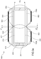
- the photovoltaic device 100 comprises a support substrate 200.
- the support substrate 200 comprises two essentially parallel faces, said front face 210 and rear face 220.
- the support substrate 200 has a planar surface, that is to say the front 210 and rear 220 faces are planar and connected by a contour 201.
- the thickness Ep, of the support substrate 200 is defined by the distance separating the front 210 and rear 220 faces.
- the thickness Ep of the support substrate may be between 50 ⁇ m and 1 mm, for example 150 ⁇ m.
- the front 210 and rear 220 may be substantially square or substantially rectangular. However, the implementation of the invention should not be limited to these two forms.
- the front 210 and rear 220 faces may have a length of between 10 mm and 300 mm, for example 156.75 mm, and a width of between 10 mm and 300 mm, for example 156.75 mm.
- the support substrate 200 may comprise at least one of the following materials: monocrystalline silicon, monocrystalline germanium, monocrystalline gallium arsenide, multi-crystalline silicon.
- the support substrate 200 may advantageously comprise a doping level of between 10 13 atm / cm 3 and 10 17 atm / cm 3 .
- doping species intended to modify the electrical properties of the material or the layer or substrate in which they are located.
- the doping species may be n-type (electron donor species) or p-type ("hole-donor" species).
- An n-type doping species for silicon may for example be phosphorus or arsenic.
- a p-type dopant species for silicon may for example be boron.
- the support substrate 200 may advantageously comprise a passivation layer 300 completely covering its surface.
- the passivation layer 300 may advantageously comprise amorphous silicon.
- the amorphous silicon may comprise a doping level less than 10 20 at / cm 3.
- the passivation layer 300 may comprise intrinsic amorphous silicon, that is to say devoid of dopant species.
- the passivation layer 300 may be formed for a layer forming technique known to those skilled in the art.
- the passivation layer 300 may be formed by a plasma enhanced chemical vapor deposition technique ("PECVD” or “Plasma Enhanced Chemical Vapor Deposition” in Anglo-Saxon terminology).
- PECVD plasma enhanced chemical vapor deposition technique
- Pasma Enhanced Chemical Vapor Deposition in Anglo-Saxon terminology.
- a passivation layer 300 comprising amorphous silicon may be formed by PECVD, at a temperature between 100 ° C and 300 ° C, and as a precursor of Silane or chlorosilane.
- the thickness of the passivation layer 300 may be between 1 nm and 30 nm.
- the photovoltaic device 100 comprises at least one photovoltaic element 230 ( Fig. 3c ) comprising a first heterojunction photovoltaic cell 410 and a second heterojunction photovoltaic cell 510 ( Fig. 3a ).
- the first heterojunction photovoltaic cell 410 includes a first emitter region 401 and a first collector region 402 disposed respectively on the front face 210 and the back face 220.
- the second heterojunction photovoltaic cell 510 comprises a second collector region 501 and a second emitter region 502 disposed respectively on the front face 210 and the back face 220.
- a first emitter region 401 adjacent the contour 201 may overflow on said contour (201).
- a second collector region 501 adjacent the contour 201 may overflow on said contour (201).
- a first collector region 402 adjacent the contour 201 may overflow on said contour (201).
- a second emitter region 502 adjacent the contour 201 may overflow on said contour (201).
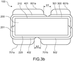
- the first heterojunction photovoltaic cell 410 and the second heterojunction photovoltaic cell 510 of the photovoltaic element 230 are electrically connected by an electrical contact before 600 ( Fig. 4a and 5a ).
- the front electrical contact 600 electrically connects the first emitter region 401 with the second collector region 501 of the photovoltaic element 230.
- the first emitter region 401 and the second collector region 501 may be of polygonal shape, advantageously of square or rectangular shape.
- the first emitter region 401 and the second collector region 501 are arranged side-by-side.
- the first collector region 402 and the second emitter region 502 are arranged side-by-side.
- Arranged side by side means that the first emitter region 401 and the second collector region 501 share one side.
- sharing a side it is meant that one side of an emitting region is adjacent to and near one side of a collector region.
- one side of the first emitter region 401 is parallel to and near one side of the second collector region 501.
- distance a1 ( figures 3a and 3c ) the distance between the first emitter region 401 and the second collector region 501 of a photovoltaic element 230.
- distance a2 the distance between the first collector region 402 and the second emitter region 502 of a photovoltaic element 230 ( figure 3a and 3c ).
- the distance a1 may be less than 2 mm, advantageously equal to 1 mm, and even more advantageously zero.
- the first emitter region 401 and the second collector region 501 of the same photovoltaic element 230 may overlap, that is, the distance a1 is negative.
- the distance a2 is strictly positive, and may be less than 2 mm, advantageously equal to 1 mm.
- the photovoltaic device 100 comprises a plurality of photovoltaic elements 230, the latter are electrically connected in series by at least one rear electrical contact 700 (FIG. Fig. 4b and 5b ).
- each rear electrical contact 700 electrically connects the first collector region 402 of a photovoltaic element 230, said first photovoltaic element, to the second emitter region 502 of another photovoltaic element 230 immediately adjacent to the first photovoltaic element.
- the photovoltaic elements 230 are then arranged side by side so that the first emitter regions 401 and the second collector regions 501 are arranged side by side and alternately.
- a regular succession of a first emitter region 401 and a second collector region 501 is meant a regular succession of a first emitter region 401 and a second collector region 501.
- a second collector region 501 does not share any side with another second conductive region.
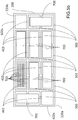
- the first emitter regions 401 and the second collector regions 501 can be arranged alternately in a row extending a direction D of the front face 210 ( Figures 4a and 4b ).
- alternation is not limited, in the sense of the present invention, to a single direction of the front face 210.
- first emitter regions 401 and the second collector regions 501 can be arranged alternately in a matrix ( figure 5a and 5b ).
- first collector regions 402 and the second emitter regions 502 are also arranged side by side and alternately on the rear face 220.
- distance a1b ( figure 3c ) the distance between the first emitter region 401 of a photovoltaic element 230, said first element, and the second collector region 501 of another photovoltaic element 230 immediately adjacent to the first element. It is understood that the first emitter region 401 of the photovoltaic element 230, said first element, and the second collector region 501 of the other photovoltaic element 230 are side-by-side on the front face 210.
- the distance a1b is strictly positive, and may be less than 2 mm, advantageously equal to 1 mm.
- the distances a1 and a1b may be identical.
- distance a2b ( figure 3c ) the distance between the first collector region 402 of a photovoltaic element 230, said first photovoltaic element, and the second emitter region 502 of another photovoltaic element 230 immediately adjacent to the first element. It is understood that the first collector region 402 of the photovoltaic element 230, said first photovoltaic element, and the second emitter region 502 of the other photovoltaic element are arranged side-by-side on the rear face 220.
- the distance a2b may be less than 2 mm, advantageously equal to 1 mm, even more advantageously zero.
- the first collector region 402 of the photovoltaic element 230, said first photovoltaic element, and the second emitter region 502 of the other photovoltaic element can be overlapped, that is, the distance a2b can be negative.
- the distances a2 and a2b may be identical, especially if the connection between adjacent regions is made by metal connectors (screen printing).
- the distances a1 and a2b are equal, even more advantageously, these two distances are negative.
- the first and second emitter regions 401 and 502, and the first and second collector regions 402 and 501 may be formed by a deposition or layer-forming technique, for example by PECVD. Their formation may involve masking, photolithography, and screen printing techniques known to those skilled in the art, and which are therefore not described in detail in the present application.
- the first and second emitter regions 401 and 502, and the first and second collector regions 402 and 501 may be n-doped or P-doped amorphous silicon layers.
- the first and second emitter regions 401 and 502 have p-type doping
- the support substrate 200 comprises n-type doping
- the first and second collector regions 402 and 501 have n-type doping.
- the first emitter regions 401 and the second emitter regions 502 comprise amorphous silicon with a p-type doping level (for example boron) of between 10 21 at / cm 3 and 5 ⁇ 10 22 at / cm 3 .
- a p-type doping level for example boron
- the first collector regions 402 and the second collector regions 501 comprise amorphous silicon with an n-type doping level (for example phosphorus or arsenic) of 10 21 at / cm 3 and 5 ⁇ 10 22 at / cm 3 .
- n-type doping level for example phosphorus or arsenic
- the first emitter regions 401 and the second emitter regions 502 are of rectangular or square shape.
- first collector regions 402 and the second collector regions 501 are of rectangular or square shape.
- the surfaces of the first emitter 401 and collector regions 402, as well as the surfaces of the second collector 501 and emitter regions 502 may be different. More particularly, said surfaces can be adjusted so that the first photovoltaic cell 410 and the second photovoltaic cell 510 have substantially identical performances, especially as regards the photo-generated and collected current.
- the front electrical contact 600 may comprise a first front electrical contact section 601a and a second electrical contact section 601b, in contact, respectively, with the first emitter region 401, and the second collector region 501 of a photovoltaic element 230 ( figure 3a and 3b ).
- the first front electrical contact section 601a and the second front electrical contact section 601b are in the form of a layer of conductive material in at least partial overlap, respectively, of the first transmitting region 401 and the second collector region 501.
- the first front electrical contact section 601a and the second front electrical contact section 601b of the front electrical contact 600 are side-by-side, and spaced apart by a distance b1 ( figures 3b and 3c ).
- the distance b1 may be less than 2 mm, or advantageously zero or negative (in overlap).
- the first front electrical contact section 601a of a photovoltaic element 230, said first photovoltaic element, and the second front electrical contact section 601b of another photovoltaic element 230 immediately adjacent to the first photovoltaic element, are spaced apart by a distance b1b ( figure 3c ).
- the distance b1b is strictly positive, and advantageously between 0.5 mm and 2 mm.
- the first front electrical contact section 601a and the second forward electrical contact section 601b may each be formed by a conductive transparent oxide layer.
- the transparent conductive oxide layer may comprise indium oxide, advantageously comprising at least one of the elements chosen from hydrogen, tungsten, cerium and cadmium; or zinc oxide comprising at least one of the elements selected from aluminum, indium and boron.
- the first front electrical contact section 601a and the second forward electrical contact section 601b can be formed by layer deposition techniques known to those skilled in the art. These techniques may involve masking steps, photolithography and or screen printing, also known to those skilled in the art.
- the first front electrical contact section 601a, and the second forward electrical contact section 601b may each be made of a different material, so as to adjust the contact resistances, respectively, between the first front electrical contact section 601a and the first front electrical contact section 601b.
- the front electrical contact 600 also includes a front metal contact section 602 (it is understood without it being necessary to specify that the forward metal contact section comprises metal).
- the front metal contact section 602 electrically connects the first front electrical contact section 601a and the second electrical contact section 601b of the front electrical contact 600.
- the front metal contact section 602 may advantageously comprise front metal fingers 602 ("fingers"). according to Anglo-Saxon terminology) ( figures 3a , 4a , 5a ).
- the front metal fingers 602 each connect the first front electrical contact section 601a and the second electrical contact section 601b of the front electrical contact 600. More particularly, the metal fingers 602 connect the free surface of the first front electrical contact section 601a and the free surface of the second electrical contact section 601b of the electrical contact before 600.
- the front metal fingers 602 of the front metal contact 600 are parallel to each other.
- the rear electrical contact 700 may comprise a first rear electrical contact section 701a and a second rear electrical contact section 701b, in contact, respectively, with the first collector region 402 of a photovoltaic element, referred to as the first photovoltaic element, at the second emitting region 502 of another photovoltaic element immediately adjacent to the first photovoltaic element.
- first rear electrical contact section 701a and the second rear electrical contact section 701b are in the form of a layer of conducting material overlapping, at least partially, respectively, of the first collector region 402 and the second emitter region 502.
- the first rear electrical contact section 701a in contact with the first collector region 402 and the second rear electrical contact section 701b in contact with the second emitter region 502 do not belong to the same rear electrical contact 700.
- the first rear electrical contact section 701a and the second rear electrical contact section 701b are side-by-side, and distant by a distance b2 ( figure 3b and 3c ).
- the distance b2 is strictly positive, and advantageously between 0.5 mm and 2 mm.
- the first rear electrical contact section 701a and the second rear electrical contact section 701b of the rear electrical contact 700 are side-by-side, and distant a distance b2b ( figure 3c ).
- the distance b2b may be less than 2 mm, or even between 0 mm and 2 mm, or between 0.5 mm and 2 mm.
- the distance b2b is zero or negative.
- the distance b2b may advantageously be less than zero. More particularly, since the distance b1b is strictly positive, the distance b2b may advantageously be less than zero.
- the first rear electrical contact section 701a and the second rear electrical contact section 701b may each be formed by a conductive transparent oxide layer.
- the transparent conductive oxide layer may comprise indium oxide, advantageously comprising at least one of the elements chosen from hydrogen, tungsten, cerium and cadmium; or zinc oxide comprising at least one of the elements selected from aluminum, indium, boron.
- the first rear electrical contact section 701a, and the second rear electrical contact section 701b may be formed by layer deposition techniques known to those skilled in the art. These techniques may involve masking steps, photolithography and or screen printing, also known to those skilled in the art.
- the first rear electrical contact section 701a, and the second rear electrical contact section 701b may each be made of a different material, so as to adjust the contact resistances, respectively, between the first rear electrical contact section 701a and the first transmitting region 401, and between second rear electrical contact section 701b and second transmitting region 502.
- the rear electrical contact 700 also includes a rear metal contact section 702 (it is understood without it being necessary to specify that the rear metal contact section comprises metal).
- the rear metal contact section 702 electrically connects the first rear electrical contact section 701a and the second rear electrical contact section 701b of the rear electrical contact 700.
- the rear metal contact section 702 may advantageously comprise rear metal fingers 702 ("fingers"). According to Anglo-Saxon terminology) ( figure 4b and 5b ).
- the rear metal fingers 702 each connect the first rear electrical contact section 701a and the second rear electrical contact section 701b of the rear electrical contact 700. More particularly, the rear metal fingers 702 connect the free surface of the first rear electrical contact section. 701a and the free surface of the second rear electrical contact section 701b of the rear electrical contact 700.
- the rear metal fingers 702 of the rear metal contact 700 are parallel to each other.
- the front 602 and rear electrical contact sections, and more particularly the front metal 602 and rear 702, can be made by screen printing, and include silver.
- At least one of the first forward electrical contact sections 601a may have one of these sides adjacent an edge of the support substrate 200.
- the spacing between said side and the edge of the substrate 200 is noted: distance c1.
- At least one of the second forward electrical contact sections 602a may have one of these sides adjacent an edge of the support substrate 200.
- the spacing between said side and the edge of the substrate 200 is noted: distance c2.
- At least one of the first rear electrical contact sections 701a may have one of these sides adjacent an edge of the support substrate 200.
- the spacing between said side and the edge of the substrate 200 is noted: distance c3.
- At least one of the second rear electrical contact sections 701b may have one of these sides adjacent an edge of the support substrate 200.
- the spacing between said side and the edge of the substrate 200 is noted: distance c4.
- a distance ci (i being equal to 1, 2, 3 or 4) is positive (greater than 0) when the electrical contact section concerned is recessed relative to the contour 201, and is said to be negative (less than 0 ) when the electrical contact section overflows over the contour 201.
- the distances c1 and c4 can be equal and positive since the first emitter region 401 and the second emitter region 502 are made of p-doped amorphous silicon, and the distances c2 and c3 can be equal and negative since the first collector region 402 and the second collector region 501 are made of n-doped amorphous silicon.
- the distances c1 and c4 can be equal and negative since the first emitter region 401 and the second emitter region 502 are made of n-doped amorphous silicon, and the distances c2 and c3 can be equal and positive since the first collector region 402 and the second collector region 501 are made of p-doped amorphous silicon.
- the photovoltaic device 100 further comprises a first end collecting region 402a and a second end emitting region 502a.
- the first end collector region 402a is one of the first collector regions 402, and the second end emitter region 502a is one of the second emitter regions 502.
- the first end collecting region 402a and the second end emitting region 502a are disposed at the end of the series electrical connection chain of the photovoltaic element (s). 230.
- the first end collecting region 402a and the second end emitting region 502a are not electrically connected to each other, respectively, second emitter region 502 and first collector region 402 of the same device via a rear electrical contact 700.
- the photovoltaic device 100 comprises only one photovoltaic element, the first end collecting region 402a and the second end emitting region 502a are, respectively, the first region collector 402 and the second emitter region 502 of said element 230 ( figure 4b ).
- the first end collecting region 402a and the second end emitting region 502a respectively comprise a first end contact 703 and a second end contact 704 ( figure 4b ).
- the first end contact 703 advantageously comprises a first end electrical contact section 703a in contact with the first region end collector 402a, as well as a first metal contact section 703b.
- the first metal contact section 703b comprises for example first metal fingers 703b arranged in parallel on the surface of the first end electrical contact section 703a.
- the second end contact 704 advantageously comprises a second end electrical contact section 704a in contact with the second end emitter region 502a, as well as a second metal contact section 704b.
- the second metal contact section 704b comprises, for example, second metal fingers 704b arranged in parallel on the surface of the second end electrical contact section 704a.
- the first end electrical contact section 703a and the second end electrical contact section 704a can be formed using techniques equivalent to those used for forming the first rear electrical contact section 701a, and the second 701b rear electrical contact section
- the first metal fingers 703b and the second metal fingers 704b can be formed using techniques equivalent to those used for the formation of the rear metal fingers 702.
- the first end collecting region 402a and the second end emitting region 502a are advantageously adjacent to the contour 201
- first collector regions 402 and the second emitter regions 502 are alternately arranged in a row extending in a direction D of the rear face 220, the first end collector region 402a and the second emitter region 502a are respectively disposed at a first end and at a second end of said row ( figure 4b ).
- the first collecting regions 402 and the second emitting regions 502 are alternately arranged in a matrix
- the first end collecting region 402a and the second end emitting region 502a are arranged, respectively, to a first corner 220a and a second corner 220b of said matrix ( figure 5b ).
- the first end collecting region 402a and the second end emitting region 502a may be for connecting a plurality of photovoltaic devices 100 when assembling a photovoltaic panel.
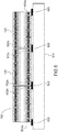
- the invention also relates to a photovoltaic panel 800 comprising photovoltaic devices 100 according to the invention ( figure 6 ).
- the photovoltaic panel comprises a support 810 on which a plurality of photovoltaic devices 100 are arranged.
- the support 810 may comprise at least one of the materials chosen from: a transparent polymer material, glass.
- At least one additional contact 820 is arranged on the photovoltaic panel and intended to electrically connect the first end contact 703 of a first photovoltaic device 100, with the second end contact 704 of another photovoltaic device 100 adjacent to the first photovoltaic device.
- the additional contact 820 may comprise at least one of the materials chosen from: copper, silver, tin, indium.
- the additional contact may be in the form of ribbon, wires, glues
- the arrangement of the photovoltaic cells makes it possible both to make the photovoltaic panel according to the invention reliable, but also to simplify its assembly process.
- the photovoltaic device 100 also makes it possible to reduce the spacing between the first and second photovoltaic cells, but also between two adjacent photovoltaic devices. The white areas are thus reduced, thus making it possible to improve the efficiency of the photovoltaic panel.
- first and second photovoltaic cells of smaller size also makes it possible to overcome the formation of busbar (a busbar is a set of conductors arranged on one side of a photovoltaic cell, and intended to electrically connect a series of parallel electrical contacts between them and in contact with said face of the cell).
- busbar is a set of conductors arranged on one side of a photovoltaic cell, and intended to electrically connect a series of parallel electrical contacts between them and in contact with said face of the cell.
- the photovoltaic panel according to the invention is bifacial, in other words said panel can convert light energy, incident on a front face and on a rear face, into electrical energy (voltage and current).
- the support 810 must be transparent, for example made of transparent polymer or glass.
- the invention further relates to a method of manufacturing the photovoltaic device 100, and which essentially takes over all the previously described process steps. More particularly, the method according to the invention includes steps of forming the first emitter region 401, the first collector region 402, the second emitter region 502, the second collector region 501, by a film deposition technique, for example by the PECVD technique.
- the passivation layer 300 may also be formed by PECVD.
- first front and rear electrical contact sections 601a and 701a can be formed by several physical or chemical vapor or non-vapor deposition techniques, assisted by plasma or not, or by printing deposit.
- the manufacturing method comprises a step a) which consists in providing the support substrate 200.
- the method also comprises a step b) of forming the at least one first emitter region 401 and the at least one second collector region 501, preferably of polygonal shape, side-by-side and alternately, on the face before 210.
- the method further comprises a step c) of forming the at least one first collector region 402 and the at least one second polygon-shaped emitter region 502 on the back face 220, and to the right, respectively, of the at least one first emitter region 401 and the at least one second collector region 501.
- the manufacturing method comprises a step d) which consists in forming the at least one electrical contact before 600 connecting the at least one first collector region 401 with the at least one second emitter region 501.
- the method may further comprise a step e) of forming at least one back electrical contact 700.
- the method may further comprise a step a1) of forming the passivation layer 300 integrally covering the support substrate 200 and so that the at least a first emitter 401 and sink region 402 and the at least one second emitter 502 and sink region 501 rely on said passivation layer 300.
Landscapes
- Photovoltaic Devices (AREA)
Applications Claiming Priority (1)
| Application Number | Priority Date | Filing Date | Title |
|---|---|---|---|
| FR1663029A FR3060852A1 (fr) | 2016-12-21 | 2016-12-21 | Dispositif photovoltaique et procede de fabrication associe |
Publications (1)
| Publication Number | Publication Date |
|---|---|
| EP3340318A1 true EP3340318A1 (de) | 2018-06-27 |
Family
ID=58347616
Family Applications (1)
| Application Number | Title | Priority Date | Filing Date |
|---|---|---|---|
| EP17209141.5A Withdrawn EP3340318A1 (de) | 2016-12-21 | 2017-12-20 | Fotovoltaik-vorrichtung und entsprechendes herstellungsverfahren |
Country Status (2)
| Country | Link |
|---|---|
| EP (1) | EP3340318A1 (de) |
| FR (1) | FR3060852A1 (de) |
Cited By (2)
| Publication number | Priority date | Publication date | Assignee | Title |
|---|---|---|---|---|
| CN113330585A (zh) * | 2018-12-21 | 2021-08-31 | 法国原子能及替代能源委员会 | 用于钝化光伏电池的方法和用于生产钝化的光伏子电池的方法 |
| US11869998B2 (en) | 2021-03-24 | 2024-01-09 | Maxeon Solar Pte. Ltd. | Cross-tied photovoltaic array |
Citations (2)
| Publication number | Priority date | Publication date | Assignee | Title |
|---|---|---|---|---|
| US4330680A (en) * | 1980-10-28 | 1982-05-18 | Fraunhofer Gesellschaft Zur Forderung Der Angewandten Forschung E.V. | Integrated series-connected solar cell |
| WO2014136083A1 (fr) * | 2013-03-08 | 2014-09-12 | Commissariat A L'energie Atomique Et Aux Energies Alternatives | Substrat semi-conducteur monolithique à base de silicium, divisé en sous-cellules |
-
2016
- 2016-12-21 FR FR1663029A patent/FR3060852A1/fr not_active Withdrawn
-
2017
- 2017-12-20 EP EP17209141.5A patent/EP3340318A1/de not_active Withdrawn
Patent Citations (2)
| Publication number | Priority date | Publication date | Assignee | Title |
|---|---|---|---|---|
| US4330680A (en) * | 1980-10-28 | 1982-05-18 | Fraunhofer Gesellschaft Zur Forderung Der Angewandten Forschung E.V. | Integrated series-connected solar cell |
| WO2014136083A1 (fr) * | 2013-03-08 | 2014-09-12 | Commissariat A L'energie Atomique Et Aux Energies Alternatives | Substrat semi-conducteur monolithique à base de silicium, divisé en sous-cellules |
Cited By (2)
| Publication number | Priority date | Publication date | Assignee | Title |
|---|---|---|---|---|
| CN113330585A (zh) * | 2018-12-21 | 2021-08-31 | 法国原子能及替代能源委员会 | 用于钝化光伏电池的方法和用于生产钝化的光伏子电池的方法 |
| US11869998B2 (en) | 2021-03-24 | 2024-01-09 | Maxeon Solar Pte. Ltd. | Cross-tied photovoltaic array |
Also Published As
| Publication number | Publication date |
|---|---|
| FR3060852A1 (fr) | 2018-06-22 |
Similar Documents
| Publication | Publication Date | Title |
|---|---|---|
| EP2452369B1 (de) | Verfahren zur herstellung von pv-zellen mit mehreren anschlüssen und mehreren elektroden | |
| WO2006077343A1 (fr) | Dispositif semi-conducteur a heterojonctions et a structure inter-digitee | |
| EP1482559A1 (de) | Infrarotdetektor mit unabhängigem, leitfähigem 3D-Gate | |
| US20110277819A1 (en) | Bifacial thin film solar panel and methods for producing the same | |
| EP2172981A2 (de) | Fotovoltaikzelle mit Heteroübergang mit zwei Dotierungen und Herstellungsverfahren | |
| EP4002491B1 (de) | Verbessertes leichtes und flexibles fotovoltaikmodul | |
| WO2015071285A1 (fr) | Cellule photovoltaique a hereojonction de silicium | |
| FR3069705A1 (fr) | Cellule photovoltaique tandem | |
| FR3083369A1 (fr) | Interconnexion monolithique de modules photovoltaiques | |
| EP3011602B1 (de) | Solarzelle mit einem silikonheteroübergang | |
| EP3340318A1 (de) | Fotovoltaik-vorrichtung und entsprechendes herstellungsverfahren | |
| EP4195297A1 (de) | Photovoltaikmodul mit integrierter gedruckter bypassdiode | |
| FR2837625A1 (fr) | Dispositif photovoltaique multi-jonctions a cellules independantes sans effet d'ombrage et procede de realisation d'un tel dispositif | |
| EP4177967A1 (de) | Photovoltaische zelle mit mindestens einer verbesserten leitfähigen transparenten oxidschicht | |
| EP4631109A1 (de) | Doppelseitiges fotovoltaisches modul | |
| EP3000136B1 (de) | Verfahren zur herstellung eines fotovoltaischen lichtkonzentrationssystems | |
| FR3026229A1 (fr) | Cellule photovoltaique a contacts en face arriere, module photovoltaique et procede de fabrication d'un tel module | |
| FR2849276A1 (fr) | Module photovoltaique integre pour systeme a concentration et un procede de fabrication | |
| US20230197864A1 (en) | Photovoltaic cell with passivated contacts and with non-reflective coating | |
| EP4386875A1 (de) | Verfahren zur herstellung einer photovoltaischen zelle | |
| EP4416764A1 (de) | Anordnung für ein photovoltaikmodul, photovoltaikmodul und verfahren zur herstellung der anordnung und des moduls | |
| EP4521887A1 (de) | Verfahren zur passivierung von solarzellen | |
| FR3142632A1 (fr) | Ensemble pour module photovoltaïque, module photovoltaïque et procédé de fabrication de l’ensemble et du module | |
| EP3671843A1 (de) | Herstellungsverfahren einer vielzahl von dioden aus einem lesesubstrat | |
| WO2025114369A1 (fr) | Cellule photovoltaïque ameliorée comprenant une interface de connexion |
Legal Events
| Date | Code | Title | Description |
|---|---|---|---|
| PUAI | Public reference made under article 153(3) epc to a published international application that has entered the european phase |
Free format text: ORIGINAL CODE: 0009012 |
|
| STAA | Information on the status of an ep patent application or granted ep patent |
Free format text: STATUS: REQUEST FOR EXAMINATION WAS MADE |
|
| 17P | Request for examination filed |
Effective date: 20171220 |
|
| AK | Designated contracting states |
Kind code of ref document: A1 Designated state(s): AL AT BE BG CH CY CZ DE DK EE ES FI FR GB GR HR HU IE IS IT LI LT LU LV MC MK MT NL NO PL PT RO RS SE SI SK SM TR |
|
| AX | Request for extension of the european patent |
Extension state: BA ME |
|
| STAA | Information on the status of an ep patent application or granted ep patent |
Free format text: STATUS: THE APPLICATION IS DEEMED TO BE WITHDRAWN |
|
| 18D | Application deemed to be withdrawn |
Effective date: 20190103 |