EP4386875A1 - Verfahren zur herstellung einer photovoltaischen zelle - Google Patents
Verfahren zur herstellung einer photovoltaischen zelle Download PDFInfo
- Publication number
- EP4386875A1 EP4386875A1 EP23214656.3A EP23214656A EP4386875A1 EP 4386875 A1 EP4386875 A1 EP 4386875A1 EP 23214656 A EP23214656 A EP 23214656A EP 4386875 A1 EP4386875 A1 EP 4386875A1
- Authority
- EP
- European Patent Office
- Prior art keywords
- substrate
- lateral
- stack
- passivation layer
- initial
- Prior art date
- Legal status (The legal status is an assumption and is not a legal conclusion. Google has not performed a legal analysis and makes no representation as to the accuracy of the status listed.)
- Pending
Links
Images


Classifications
-
- H—ELECTRICITY
- H10—SEMICONDUCTOR DEVICES; ELECTRIC SOLID-STATE DEVICES NOT OTHERWISE PROVIDED FOR
- H10F—INORGANIC SEMICONDUCTOR DEVICES SENSITIVE TO INFRARED RADIATION, LIGHT, ELECTROMAGNETIC RADIATION OF SHORTER WAVELENGTH OR CORPUSCULAR RADIATION
- H10F71/00—Manufacture or treatment of devices covered by this subclass
- H10F71/121—The active layers comprising only Group IV materials
Definitions
- the invention relates to the technical field of photovoltaic cells, in particular photovoltaic cells comprising a passivated contact on each of the surfaces of the substrate.
- passivation we mean the neutralization of electrically active defects on the surfaces of the substrate. Indeed, a surface of a crystalline silicon substrate has a density of defects (e.g. dangling bonds, impurities, discontinuity of the crystal, etc.) which can lead to significant losses linked to surface recombination of carriers in the case of a photovoltaic application.
- passivated contacts There are several types of passivated contacts. Mention may in particular be made of a passivated contact based on hydrogenated amorphous silicon, or even a passivated contact comprising a tunnel oxide film and a layer of doped polycrystalline silicon.
- the invention finds particular application in the manufacture of heterojunction silicon type photovoltaic cells (ie amorphous silicon/crystalline silicon heterojunction).
- other photovoltaic cell architectures are possible, for example a TOPCon type architecture (" Tunnel Oxide Passivated Contact" in English) where the passivated contact comprises a tunnel oxide film and a layer of doped polycrystalline silicon, or again a monolithic multi-junction type architecture (eg silicon/perovskite tandem cell).
- the first lateral edge of the substrate and the first lateral part of the stack of active layers constitute a so-called native edge of the initial photovoltaic cell.
- the second lateral edge of the substrate and the second lateral part of the stack of active layers also constitute a native edge of the initial photovoltaic cell.
- the third lateral edge of the substrate and the third lateral part of the stack of active layers constitute a native edge of the initial photovoltaic cell.
- the fourth lateral edge of the substrate and the fourth lateral part of the stack of active layers constitute a native edge of the initial photovoltaic cell.
- Such a method according to the invention makes it possible to improve the quality of passivation of the photovoltaic sub-cells which will be obtained after step c 1 ), thanks to steps b 1 ) and c 1 ) making it possible to replace the edge native to the initial photovoltaic cell, formed by the first lateral edge of the substrate and the first lateral part of the stack of active layers.
- the first passivation layer having an effective surface recombination speed strictly lower than SRVo, is of better quality than the initial passivation layer.
- the inventors have found, surprisingly, that the performance of the photovoltaic sub-cells is limited by the quality of the passivation of the native edges of the initial photovoltaic cell.
- those skilled in the art conventionally retain the native edges of the initial photovoltaic cell and concentrate on the passivation of the cut edges when obtaining functional photovoltaic sub-cells.
- the native edges of the initial photovoltaic cell are relatively sensitive, and susceptible to shocks or scratches which can deteriorate the quality of passivation, and thereby reduce the efficiency of the photovoltaic sub-cells.
- the native edges of the initial photovoltaic cell generally have a lower intrinsic passivation quality than the upper and lower surfaces of the substrate (deposition quality, layer uniformity, etc.).
- the method according to the invention may include one or more of the following characteristics.
- an advantage provided is to improve the quality of passivation of the photovoltaic sub-cells which will be obtained after step c 2 ), thanks to steps b 2 ) and c 2 ) making it possible to replace the native edge of the cell initial photovoltaic, formed by the second lateral edge of the substrate and the second lateral part of the stack of active layers.
- an advantage provided is to improve the quality of passivation of the photovoltaic sub-cells which will be obtained after step c 3 ), thanks to steps b 3 ) and c 3 ) making it possible to replace the native edge of the cell initial photovoltaic, formed by the third lateral edge of the substrate and the third lateral part of the stack of active layers.
- an advantage provided is to improve the quality of passivation of the photovoltaic sub-cells which will be obtained after step c 4 ), thanks to steps b 4 ) and c 4 ) making it possible to replace the native edge of the cell initial photovoltaic, formed by the fourth lateral edge of the substrate and the fourth lateral part of the stack of active layers.
- the inventors noted, by simulation, a potential increase of 0.1% in yield of the initial photovoltaic cell (before the formation of sub-photovoltaic cells) per replaced native edge.
- an advantage provided is to improve the performance of the initial photovoltaic cell by completely eliminating the initial dropout (classically a clipping zone) which is a source of electrical losses (electrical shading), in particular for a silicon type architecture with heterojunction.
- step b 2 is carried out by a second cutting of the substrate adjusted to remove the second lateral part of the stack of active layers and a second lateral zone of the substrate, so that the second edge side of the substrate reached at the end of the second cutting faces the initial separation of the superficial conductive transparent oxide layer.
- an advantage provided is to improve the performance of the initial photovoltaic cell by completely eliminating the initial dropout (classically a clipping zone) which is a source of electrical losses (electrical shading), in particular for a silicon type architecture with heterojunction.
- step b 3 is carried out by a third cutting of the substrate adjusted to remove the third lateral part of the stack of active layers and a third lateral zone of the substrate, so that the third edge side of the substrate reached at the end of the third cut faces the initial separation of the superficial conductive transparent oxide layer.
- an advantage provided is to improve the performance of the initial photovoltaic cell by completely eliminating the initial dropout (classically a zone of clipping) which is a source of electrical losses (electrical shading), in particular for a silicon heterojunction type architecture.
- step b 4 is carried out by a fourth cutting of the substrate adjusted to remove the fourth lateral part of the stack of active layers and a fourth lateral zone of the substrate, so that the fourth edge side of the substrate reached at the end of the fourth cut faces the initial separation of the superficial conductive transparent oxide layer.
- an advantage provided is to improve the performance of the initial photovoltaic cell by completely eliminating the initial dropout (classically a clipping zone) which is a source of electrical losses (electrical shading), in particular for a silicon type architecture with heterojunction.
- said at least two photovoltaic sub-cells have cut edges at the end of step d); the method comprising a step e) consisting of coating each edge cut at the end of step d) with a passivation layer having an effective surface recombination speed strictly less than SRV 0 .
- step a) is carried out so that the initial passivation layer is produced in hydrogenated amorphous silicon; and step c 1 ) is carried out so that the first passivation layer is made from an aluminum oxide.
- hydrogenated amorphous silicon has a passivation potential generally greater than that of aluminum oxide
- the presence of hydrogenated amorphous silicon on a lateral edge of the substrate leads to a poorer quality of intrinsic passivation (eg limitations in terms of deposit and uniformity) and to greater sensitivity to shock, damage, and contamination.
- the use of aluminum oxide therefore makes it possible to reduce the effective surface recombination speed compared to the hydrogenated amorphous silicon present on a lateral edge.
- the use of optically transparent aluminum oxide is advantageous from an integration point of view because the aluminum oxide can be deposited without impact on the entire lateral surface of the photovoltaic cell, on the contrary amorphous silicon.
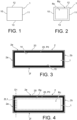
- Substrate 1 is based on crystalline silicon. Substrate 1 is advantageously made from monocrystalline silicon, preferably n-type doped.
- the substrate 1 has an upper edge 14 and an opposite lower edge 15, connecting the side edges 10, 11, 12, 13.
- the upper edge 14 and/or the lower edge 15 are intended to be exposed to light radiation.
- the upper edge 14 may be intended to form the front face of the cell photovoltaic, while the lower edge 15 can be intended to form the rear face of the photovoltaic cell.
- the initial photovoltaic cell further comprises a stack 2 of active layers 20, formed around the substrate 1.
- the stack 2 of active layers 20 comprises an initial passivation layer P0 having an effective surface recombination speed, denoted SRV 0 .
- the initial passivation layer P0 is formed on the first and second side edges 10, 11, on the third and fourth side edges 12, 13, as well as on the upper and lower edges 14, 15.
- the initial passivation layer P0 can be made in a hydrogenated amorphous silicon, denoted a-Si:H. Hydrogenated amorphous silicon is intrinsic.
- the initial passivation layer P0 of the upper and lower parts 2e, 2f of the stack 2 of active layers 20 may have an effective surface recombination speed slightly lower than that of the lateral parts 2a, 2b, 2c, 2d.
- the stack 2 of active layers 20 may include a charge separation layer formed on the initial passivation layer P0.
- the charge separation layer of the upper part 2e of the stack 2 is doped with a first type.
- the charge separation layer of the lower part 2f of the stack 2 is doped with a second type, opposite to the first type.
- the charge separation layer can be made of a-Si:H.
- the upper and lower parts 2e, 2f of the stack 2 may comprise additional active layers 20 (not illustrated), such as transparent conductive oxides (e.g. indium-tin oxide ITO), metal pads forming electrodes , anti-reflective layers etc.
- Step a) can be carried out so that the lower part 2f of the stack 2 comprises a surface layer of transparent conductive oxide 200 having an initial recess, set back relative to each lateral edge 10, 11,12, 13 of the substrate 1.
- the initial separation is preferably obtained by trimming.
- the initial drop can be of the order of 1 mm.
- the superficial conductive transparent oxide layer 200 can be made of indium-tin oxide ITO.
- the peripheral region Rp comprises the first and second side edges 10, 11 of the substrate 1, as well as the third and fourth side edges 12, 13 of the substrate 1.
- the peripheral region Rp also includes the upper and lower edges 14, 15 of the substrate 1 .
- the first lateral edge 10 of the substrate 1 and the first lateral part 2a of the stack 2 of active layers 20 constitute a so-called native edge of the initial photovoltaic cell.
- the second lateral edge 11 of the substrate 1 and the second lateral part 2b of the stack 2 of active layers 20 also constitute a native edge of the initial photovoltaic cell.
- the third lateral edge 12 of the substrate 1 and the third lateral part 2c of the stack 2 of active layers 20 constitute a native edge of the initial photovoltaic cell.
- the fourth lateral edge 13 of the substrate 1 and the fourth lateral part 2d of the stack 2 of active layers 20 constitute a native edge of the initial photovoltaic cell.
- the upper and lower edges 14, 15 of the substrate 1 have upper and lower surfaces respectively.
- the upper and lower surfaces may be flat.
- the top and bottom surfaces can be textured to reduce the reflection coefficient and optical losses in the initial photovoltaic cell.
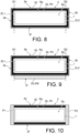
- the method comprises a step b 1 ) consisting of removing the first lateral part 2a of the stack 2 of active layers 20 so as to reach the first lateral edge 10 of the substrate 1.
- Step b 1 ) is advantageously executed by a first cutting D1 of the substrate 1 adjusted to remove the first lateral part 2a of the stack 2 of active layers 20.
- the first cutting D1 is executed in the peripheral region Rp of the substrate 1.
- the first cutting D1 is accompanied by a removal of 'a first lateral zone ZL1 of the substrate 1 extending in the peripheral region Rp of the substrate 1.
- the first lateral edge 10 of the substrate 1 reached at the end of step b 1 ) does not coincide perfectly with the first lateral edge 10 initial.
- the distance between the first initial side edge 10 and the first side edge 10 reached at the end of step b 1 ) can be between 250 ⁇ m and 1.5 mm for a substrate 1 300 mm side.
- the first cutout D1 is adjusted so that the first lateral zone ZL1 has the smallest possible surface area.
- step b 1 is advantageously executed by a first cutout D1 of the substrate 1 adjusted to remove the first lateral part 2a of the stack 2 of active layers 20 and a first lateral zone ZL1 of the substrate 1, so that the first lateral edge 10 of the substrate 1 reaches at the outcome of the first cut D1 faces the initial separation of the surface layer of transparent conductive oxide 200.
- the first cut D1 can be carried out by a laser cleavage technique (LDC for " Laser Direct Cleavage” in English), or by a laser thermal separation technique (TLS for " Thermal Laser Separation”). » in English), these techniques being known to those skilled in the art.
- the method advantageously comprises a step b 2 ) consisting of removing the second lateral part 2b of the stack 2 of active layers 20 so as to reach the second lateral edge 11 of the substrate 1.
- Step b 2 ) is advantageously executed by a second cutout D2 of the substrate 1 adjusted to remove the second lateral part 2b of the stack 2 of active layers 20.
- the second cutout D2 is executed in the peripheral region Rp of the substrate 1.
- the second cutout D2 is accompanied by a withdrawal of a second lateral zone ZL2 of the substrate 1 extending in the peripheral region Rp of the substrate 1.
- the second lateral edge 11 of the substrate 1 reached at the end of step b 2 ) does not coincide perfectly with the second initial side edge 11.
- the distance between the second initial side edge 11 and the second side edge 11 reached at the end of step b 2 ) can be between 250 ⁇ m and 1.5 mm for a substrate 1 300 mm side.
- the second cutout D2 is adjusted so that the second lateral zone ZL2 has the smallest possible surface area.
- step b 2 is advantageously carried out by a second cutout D2 of the substrate 1 adjusted to remove the second lateral part 2b of the stack 2 of active layers 20 and a second lateral zone ZL2 of the substrate 1, so that the second lateral edge 11 of the substrate 1 reached at the end of the second cutting D2 faces the initial separation of the layer of transparent conductive oxide 200 superficial.
- the second cut D2 can be carried out by a laser cleavage technique (LDC for “ Laser Direct Cleavage” in English), or by a laser thermal separation technique (TLS for “ Thermal Laser Separation”). » in English), these techniques being known to those skilled in the art.
- the method advantageously comprises a step b 3 ) consisting of removing the third lateral part 2c of the stack 2 of active layers 20 so as to reach the third lateral edge 12 of the substrate 1.
- Step b 3 ) is advantageously executed by a third cutout D3 of substrate 1 adjusted to remove the third lateral part 2c of stack 2 of active layers 20.
- the third cutting D3 is executed in the peripheral region Rp of the substrate 1.
- the third cutting D3 is accompanied by a removal of a third lateral zone ZL3 of the substrate 1 extending in the peripheral region Rp of the substrate 1.
- the third lateral edge 12 of the substrate 1 reached at the end of step b 3 ) does not coincide perfectly with the initial third lateral edge 12.
- the distance between the third initial lateral edge 12 and the third lateral edge 12 reached at the end of step b 3 ) can be between 250 ⁇ m and 1.5 mm for a substrate 1 300 mm side.
- the third cutout D3 is adjusted so that the third lateral zone ZL3 has the smallest possible surface area.
- the third cut D3 can be carried out by a laser cleavage technique (LDC for “ Laser Direct Cleavage” in English), or by a laser thermal separation technique (TLS for “Thermal Laser Separation”). » in English), these techniques being known to those skilled in the art.
- the method advantageously comprises a step b 4 ) consisting of removing the fourth lateral part 2d of the stack 2 of active layers 20 so as to reach the fourth lateral edge 13 of the substrate 1.
- Step b 4 ) is advantageously executed by a fourth cutout D4 of the substrate 1 adjusted to remove the fourth lateral part 2d of the stack 2 of active layers 20.
- the fourth cutout D4 is executed in the peripheral region Rp of the substrate 1.
- the fourth cutout D4 is accompanied by a withdrawal of a fourth lateral zone ZL4 of the substrate 1 extending in the peripheral region Rp of the substrate 1.
- the fourth lateral edge 13 of the substrate 1 reached at the end of step b 4 ) does not coincide perfectly with the fourth lateral edge 13 initial.
- the distance between the initial fourth lateral edge 13 and the fourth lateral edge 13 reached at the end of step b 4 ) can be between 250 ⁇ m and 1.5 mm for a substrate 1 300 mm side.
- the fourth cutout D4 is adjusted so that the fourth side zone ZL4 has the smallest possible surface area.
- the fourth cut D4 can be carried out by a laser cleavage technique (LDC for " Laser Direct Cleavage” in English), or by a laser thermal separation technique (TLS for " Thermal Laser Separation”). » in English), these techniques being known to those skilled in the art.
- steps b 1 ), b 2 ), b 3 ) and b 4 ) is irrelevant.
- the order of execution of steps b i ), “i” being an integer between 2 and 4 depending on the number of native edges removed, is irrelevant.
- steps b 1 ), b 2 ), b 3 ) and b 4 can be executed concomitantly.
- steps b 1 ), b 2 ), b 3 ) and b 4 can be executed concomitantly.
- steps b 1 ), “i” being an integer between 2 and 4 depending on the number of native edges removed can be executed concomitantly.
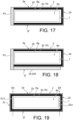
- the method comprises a step c 1 ) consisting of forming a first passivation layer P1 on the first lateral edge 10 of the substrate 1 reached at the end of step b 1 ).
- the first passivation layer P1 has an effective surface recombination speed strictly less than SRV 0 . More precisely, the first passivation layer P1 has an effective surface recombination speed strictly lower than that of the initial passivation layer P0 of the lateral parts 2a, 2b, 2c, 2d of the stack 2. It should be noted that the effective surface recombination speed of the first passivation layer P1 depends on the technique of the first cutting D1 of step b 1 ).
- step c 1 when the initial passivation layer P0 is made in a hydrogenated amorphous silicon, step c 1 ) can be carried out so that the first passivation layer P1 is made in an aluminum oxide.
- Step c 1 ) is carried out by a deposition technique adapted to the material of the first passivation layer P1.
- step c 1 ) when the first passivation layer P1 is produced in an aluminum oxide, step c 1 ) can be carried out by a deposition of atomic layers (ALD for “ Atomic Layer Deposition ” in English). ) with thermal annealing at a temperature between 100°C and 600°C.
- ALD Atomic Layer Deposition
- the first lateral edge 10 of the substrate 1 reached at the end of step b 1 ), passivated by the first passivation layer P1 may present a density of defects at the interface (" Said”, density of interface states) less than or equal to 10 9 .
- the method advantageously comprises a step c 2 ) consisting of forming a second passivation layer P2 on the second lateral edge 11 of the substrate 1 reached at the end of step b 2 ).
- the second passivation layer P2 has an effective surface recombination speed strictly lower than SRV 0 . More precisely, the second passivation layer P2 has an effective surface recombination speed strictly lower than that of the initial passivation layer P0 of the lateral parts 2a, 2b, 2c, 2d of the stack 2. It should be noted that the effective surface recombination speed of the second passivation layer P2 depends on the technique of the second cutting D2 of step b 2 ).
- step c 2 when the initial passivation layer P0 is made in a hydrogenated amorphous silicon, step c 2 ) can be carried out so that the second passivation layer P2 is made in an aluminum oxide.
- Step c 2 ) is carried out by a deposition technique adapted to the material of the second layer of P2 passivation.
- step c 2 ) when the second passivation layer P2 is produced in an aluminum oxide, step c 2 ) can be carried out by a deposition of atomic layers (ALD for “ Atomic Layer Deposition ” in English). ) with thermal annealing at a temperature between 100°C and 600°C.
- ALD Atomic Layer Deposition
- the second lateral edge 11 of the substrate 1 reached at the end of step b 2 ), passivated by the second passivation layer P2 may present a density of defects at the interface (" Said”, density of interface states) less than or equal to 10 9 .
- the method advantageously comprises a step c 3 ) consisting of forming a third passivation layer P3 on the third lateral edge 12 of the substrate 1 reached at the end of step b 3 ).
- the third passivation layer P3 has an effective surface recombination speed strictly lower than SRV 0 . More precisely, the third passivation layer P3 has an effective surface recombination speed strictly lower than that of the initial passivation layer P0 of the lateral parts 2a, 2b, 2c, 2d of the stack 2. It should be noted that the effective surface recombination speed of the third passivation layer P3 depends on the technique of the third cutting D3 of step b 3 ).
- step c 3 when the initial passivation layer P0 is made in a hydrogenated amorphous silicon, step c 3 ) can be carried out so that the third passivation layer P3 is made in an aluminum oxide.
- Step c 3 ) is carried out by a deposition technique adapted to the material of the third passivation layer P3.
- step c 3 ) when the third passivation layer P3 is produced in an aluminum oxide, step c 3 ) can be carried out by a deposition of atomic layers (ALD for “Atomic Layer Deposition ” in English). ) with thermal annealing at a temperature between 100°C and 600°C.
- the third lateral edge 12 of the substrate 1 reached at the end of step b 3 ), passivated by the third passivation layer P3, may present a density of defects at the interface (" Said”, density of interface states) less than or equal to 10 9 .
- the method advantageously comprises a step c 4 ) consisting of forming a fourth passivation layer P4 on the fourth lateral edge 13 of the substrate 1 reached at the end of step b 4 ).
- the fourth passivation layer P4 has an effective surface recombination speed strictly lower than SRV 0 . More precisely, the fourth passivation layer P4 has an effective surface recombination speed strictly lower than that of the initial passivation layer P0 of the lateral parts 2a, 2b, 2c, 2d of the stack 2. It should be noted that the effective surface recombination speed of the fourth passivation layer P4 depends on the technique of the fourth cutting D4 of step b 4 ).
- step c 4 when the initial passivation layer P0 is made in a hydrogenated amorphous silicon, step c 4 ) can be carried out so that the fourth passivation layer P4 is made in an aluminum oxide.
- Step c 4 ) is carried out by a deposition technique adapted to the material of the fourth passivation layer P4.
- step c 4 ) when the fourth passivation layer P4 is produced in an aluminum oxide, step c 4 ) can be carried out by a deposition of atomic layers (ALD for “Atomic Layer Deposition ” in English). ) with thermal annealing at a temperature between 100°C and 600°C.
- the fourth lateral edge 13 of the substrate 1 reached at the end of step b 4 ), passivated by the fourth passivation layer P4, may present a density of defects at the interface (" Said”, density of interface states) less than or equal to 10 9 .
- steps c 1 ), c 2 ), c 3 ) and c 4 ) is irrelevant.
- the order of execution of steps c i ), “i” being an integer between 2 and 4 depending on the number of native edges removed, is irrelevant.
- steps c 1 ), c 2 ), c 3 ) and c 4 ) can be executed concomitantly.
- steps c i ), “i” being an integer between 2 and 4 depending on the number of native edges removed, can be executed concomitantly.
- the materials of the first, second, third and fourth passivation layers P1, P2, P3, P4 are advantageously identical.
- the method advantageously comprises a step d) consisting of cutting the substrate 1 along at least one cutting line L1, L2 extending in the central region Rc so as to obtain at least two photovoltaic sub-cells C.
- step d) can be carried out by a laser cleavage technique (LDC for “ Laser Direct Cleavage” in English), or by a laser thermal separation technique (TLS for “ Thermal Laser Separation” in English), these techniques being known to those skilled in the art.
- Step d) is advantageously carried out so as to obtain at least two photovoltaic sub-cells C having identical surface areas.
- Step d) is advantageously carried out so that said at least one cutting line L1, L2 is parallel to the normal to the upper and lower surfaces of the substrate 1.
- Step d) is advantageously executed after steps b 1 ), b 2 ), b 3 ) and b 4 ).
- step d) is advantageously executed after steps b i ), “i” being an integer between 1 and 4 depending on the number of native edges removed.
- Step d) is advantageously executed before steps c 1 ), c 2 ), c 3 ) and c 4 ).
- step d) is advantageously executed before steps c i ), “i” being an integer between 1 and 4 depending on the number of native edges removed.
- Said at least two photovoltaic sub-cells C have cut edges at the end of step d).
- the method advantageously comprises a step e) consisting of coating each edge cut at the end of step d) with a passivation layer P' having an effective surface recombination speed strictly less than SRV 0 . More precisely, the passivation layer P' has an effective surface recombination speed strictly lower than that of the initial passivation layer P0 of the lateral parts 2a, 2b, 2c, 2d of the stack 2.
- step e) is advantageously executed concomitantly with steps c 1 ), c 2 ), c 3 ) and c 4 ).
- the passivation layer P' of step e) is advantageously made of the same material as the first, second, third and fourth passivation layers P1, P2, P3, P4.
Landscapes
- Photovoltaic Devices (AREA)
Applications Claiming Priority (1)
| Application Number | Priority Date | Filing Date | Title |
|---|---|---|---|
| FR2213602A FR3143856B1 (fr) | 2022-12-16 | 2022-12-16 | Procédé de fabrication d’une cellule photovoltaïque |
Publications (1)
| Publication Number | Publication Date |
|---|---|
| EP4386875A1 true EP4386875A1 (de) | 2024-06-19 |
Family
ID=85278230
Family Applications (1)
| Application Number | Title | Priority Date | Filing Date |
|---|---|---|---|
| EP23214656.3A Pending EP4386875A1 (de) | 2022-12-16 | 2023-12-06 | Verfahren zur herstellung einer photovoltaischen zelle |
Country Status (2)
| Country | Link |
|---|---|
| EP (1) | EP4386875A1 (de) |
| FR (1) | FR3143856B1 (de) |
Citations (2)
| Publication number | Priority date | Publication date | Assignee | Title |
|---|---|---|---|---|
| US20220005964A1 (en) * | 2018-09-24 | 2022-01-06 | Fraunhofer-Gesellschaft zur Förderung der angewandten Forschung e.V. | Seminconductor component and method for singulating a semiconductor component having a pn junction |
| US20220059718A1 (en) * | 2020-08-21 | 2022-02-24 | Jinko Green Energy (Shanghai) Management Co., LTD | Method for passivating silicon-based semiconductor device, and silicon-based semiconductor device |
-
2022
- 2022-12-16 FR FR2213602A patent/FR3143856B1/fr active Active
-
2023
- 2023-12-06 EP EP23214656.3A patent/EP4386875A1/de active Pending
Patent Citations (2)
| Publication number | Priority date | Publication date | Assignee | Title |
|---|---|---|---|---|
| US20220005964A1 (en) * | 2018-09-24 | 2022-01-06 | Fraunhofer-Gesellschaft zur Förderung der angewandten Forschung e.V. | Seminconductor component and method for singulating a semiconductor component having a pn junction |
| US20220059718A1 (en) * | 2020-08-21 | 2022-02-24 | Jinko Green Energy (Shanghai) Management Co., LTD | Method for passivating silicon-based semiconductor device, and silicon-based semiconductor device |
Non-Patent Citations (1)
| Title |
|---|
| MUNZER ANNA ET AL: "Post-Separation Processing for Silicon Heterojunction Half Solar Cells With Passivated Edges", IEEE JOURNAL OF PHOTOVOLTAICS, IEEE, vol. 11, no. 6, 10 August 2021 (2021-08-10), pages 1343 - 1349, XP011884405, ISSN: 2156-3381, [retrieved on 20211019], DOI: 10.1109/JPHOTOV.2021.3099732 * |
Also Published As
| Publication number | Publication date |
|---|---|
| FR3143856B1 (fr) | 2025-11-21 |
| FR3143856A1 (fr) | 2024-06-21 |
Similar Documents
| Publication | Publication Date | Title |
|---|---|---|
| EP2172981B1 (de) | Fotovoltaikzelle mit Heteroübergang mit zwei Dotierungen und Herstellungsverfahren | |
| EP3900052B1 (de) | Verfahren zur passivierung von fotovoltaischen zellen und verfahren zur herstellung passivierter fotovoltaischer unterzellen | |
| EP2091086A2 (de) | Halbleitervorrichtung mit Heteroübergängen | |
| EP2190024A1 (de) | Fotoelektrische Vorrichtung mit Multi-Schnittstellen und ihr Umsetzungsverfahren | |
| EP4177967A1 (de) | Photovoltaische zelle mit mindestens einer verbesserten leitfähigen transparenten oxidschicht | |
| EP3840060B1 (de) | Verfahren zur musterbildung auf der oberfläche eines kristallinen siliziumsubstrats | |
| EP3353815A1 (de) | Verfahren zur herstellung von strukturen für eine fotovoltaische zelle | |
| EP4386875A1 (de) | Verfahren zur herstellung einer photovoltaischen zelle | |
| EP2190023A1 (de) | Fotoelektrische Vorrichtung mit Multi-Schnittstellen und ihr Umsetzungsverfahren | |
| EP3761378A1 (de) | Passivierungsverfahren | |
| EP3000136B1 (de) | Verfahren zur herstellung eines fotovoltaischen lichtkonzentrationssystems | |
| EP3340318A1 (de) | Fotovoltaik-vorrichtung und entsprechendes herstellungsverfahren | |
| FR3038143A1 (fr) | Procede d'isolation des bords d'une cellule photovoltaique a heterojonction | |
| FR3004002A1 (fr) | Procede d'assemblage avance de cellule photovoltaique concentree | |
| FR3142835A1 (fr) | Procédé de fabrication de sous-cellules photovoltaïques | |
| EP4199122A1 (de) | Photovoltaische zelle mit passiven kontakten und antireflexionsbeschichtung | |
| EP4521887A1 (de) | Verfahren zur passivierung von solarzellen | |
| FR3154233A1 (fr) | Procédé de fabrication de sous-cellules photovoltaïques | |
| FR3152636A1 (fr) | Procédé de passivation de cellules photovoltaïques | |
| EP2461362A1 (de) | Fotovoltaik-Sonnenkollektor mit Dioden in Dünnschichten | |
| EP4336569A1 (de) | Photovoltaische zelle mit doppelseitenigen passivkontakten und mit unter den vorderen metallisierungen lokalisierten tco-teilen | |
| FR3142632A1 (fr) | Ensemble pour module photovoltaïque, module photovoltaïque et procédé de fabrication de l’ensemble et du module | |
| FR2948498A1 (fr) | Panneau solaire photovoltaique a diodes en couches minces | |
| WO2025114369A1 (fr) | Cellule photovoltaïque ameliorée comprenant une interface de connexion | |
| FR2910712A1 (fr) | Heterojonction a interface dopee |
Legal Events
| Date | Code | Title | Description |
|---|---|---|---|
| PUAI | Public reference made under article 153(3) epc to a published international application that has entered the european phase |
Free format text: ORIGINAL CODE: 0009012 |
|
| STAA | Information on the status of an ep patent application or granted ep patent |
Free format text: STATUS: REQUEST FOR EXAMINATION WAS MADE |
|
| 17P | Request for examination filed |
Effective date: 20231206 |
|
| AK | Designated contracting states |
Kind code of ref document: A1 Designated state(s): AL AT BE BG CH CY CZ DE DK EE ES FI FR GB GR HR HU IE IS IT LI LT LU LV MC ME MK MT NL NO PL PT RO RS SE SI SK SM TR |
|
| RAP3 | Party data changed (applicant data changed or rights of an application transferred) |
Owner name: COMMISSARIAT A L'ENERGIE ATOMIQUE ET AUX ENERGIESALTERNATIVES |