EP3340320A1 - Prozessverfahren mit verwendung eines photokonverters für organisches silikonharz zur bond-verpackung einer led durch tandemwalzen - Google Patents
Prozessverfahren mit verwendung eines photokonverters für organisches silikonharz zur bond-verpackung einer led durch tandemwalzen Download PDFInfo
- Publication number
- EP3340320A1 EP3340320A1 EP15901631.0A EP15901631A EP3340320A1 EP 3340320 A1 EP3340320 A1 EP 3340320A1 EP 15901631 A EP15901631 A EP 15901631A EP 3340320 A1 EP3340320 A1 EP 3340320A1
- Authority
- EP
- European Patent Office
- Prior art keywords
- led
- cured
- semi
- sheet
- package elements
- Prior art date
- Legal status (The legal status is an assumption and is not a legal conclusion. Google has not performed a legal analysis and makes no representation as to the accuracy of the status listed.)
- Granted
Links
Images


Classifications
-
- H—ELECTRICITY
- H10—SEMICONDUCTOR DEVICES; ELECTRIC SOLID-STATE DEVICES NOT OTHERWISE PROVIDED FOR
- H10H—INORGANIC LIGHT-EMITTING SEMICONDUCTOR DEVICES HAVING POTENTIAL BARRIERS
- H10H20/00—Individual inorganic light-emitting semiconductor devices having potential barriers, e.g. light-emitting diodes [LED]
- H10H20/01—Manufacture or treatment
- H10H20/036—Manufacture or treatment of packages
- H10H20/0362—Manufacture or treatment of packages of encapsulations
-
- H—ELECTRICITY
- H10—SEMICONDUCTOR DEVICES; ELECTRIC SOLID-STATE DEVICES NOT OTHERWISE PROVIDED FOR
- H10H—INORGANIC LIGHT-EMITTING SEMICONDUCTOR DEVICES HAVING POTENTIAL BARRIERS
- H10H20/00—Individual inorganic light-emitting semiconductor devices having potential barriers, e.g. light-emitting diodes [LED]
- H10H20/80—Constructional details
- H10H20/85—Packages
- H10H20/8506—Containers
-
- H—ELECTRICITY
- H10—SEMICONDUCTOR DEVICES; ELECTRIC SOLID-STATE DEVICES NOT OTHERWISE PROVIDED FOR
- H10H—INORGANIC LIGHT-EMITTING SEMICONDUCTOR DEVICES HAVING POTENTIAL BARRIERS
- H10H20/00—Individual inorganic light-emitting semiconductor devices having potential barriers, e.g. light-emitting diodes [LED]
- H10H20/80—Constructional details
- H10H20/85—Packages
- H10H20/851—Wavelength conversion means
- H10H20/8511—Wavelength conversion means characterised by their material, e.g. binder
-
- H—ELECTRICITY
- H10—SEMICONDUCTOR DEVICES; ELECTRIC SOLID-STATE DEVICES NOT OTHERWISE PROVIDED FOR
- H10H—INORGANIC LIGHT-EMITTING SEMICONDUCTOR DEVICES HAVING POTENTIAL BARRIERS
- H10H20/00—Individual inorganic light-emitting semiconductor devices having potential barriers, e.g. light-emitting diodes [LED]
- H10H20/80—Constructional details
- H10H20/85—Packages
- H10H20/851—Wavelength conversion means
- H10H20/8514—Wavelength conversion means characterised by their shape, e.g. plate or foil
-
- H—ELECTRICITY
- H10—SEMICONDUCTOR DEVICES; ELECTRIC SOLID-STATE DEVICES NOT OTHERWISE PROVIDED FOR
- H10H—INORGANIC LIGHT-EMITTING SEMICONDUCTOR DEVICES HAVING POTENTIAL BARRIERS
- H10H20/00—Individual inorganic light-emitting semiconductor devices having potential barriers, e.g. light-emitting diodes [LED]
- H10H20/80—Constructional details
- H10H20/85—Packages
- H10H20/852—Encapsulations
- H10H20/854—Encapsulations characterised by their material, e.g. epoxy or silicone resins
-
- H—ELECTRICITY
- H10—SEMICONDUCTOR DEVICES; ELECTRIC SOLID-STATE DEVICES NOT OTHERWISE PROVIDED FOR
- H10H—INORGANIC LIGHT-EMITTING SEMICONDUCTOR DEVICES HAVING POTENTIAL BARRIERS
- H10H29/00—Integrated devices, or assemblies of multiple devices, comprising at least one light-emitting semiconductor element covered by group H10H20/00
- H10H29/10—Integrated devices comprising at least one light-emitting semiconductor component covered by group H10H20/00
- H10H29/14—Integrated devices comprising at least one light-emitting semiconductor component covered by group H10H20/00 comprising multiple light-emitting semiconductor components
-
- H—ELECTRICITY
- H10—SEMICONDUCTOR DEVICES; ELECTRIC SOLID-STATE DEVICES NOT OTHERWISE PROVIDED FOR
- H10W—GENERIC PACKAGES, INTERCONNECTIONS, CONNECTORS OR OTHER CONSTRUCTIONAL DETAILS OF DEVICES COVERED BY CLASS H10
- H10W90/00—Package configurations
-
- B—PERFORMING OPERATIONS; TRANSPORTING
- B32—LAYERED PRODUCTS
- B32B—LAYERED PRODUCTS, i.e. PRODUCTS BUILT-UP OF STRATA OF FLAT OR NON-FLAT, e.g. CELLULAR OR HONEYCOMB, FORM
- B32B37/00—Methods or apparatus for laminating, e.g. by curing or by ultrasonic bonding
- B32B37/12—Methods or apparatus for laminating, e.g. by curing or by ultrasonic bonding characterised by using adhesives
- B32B2037/1253—Methods or apparatus for laminating, e.g. by curing or by ultrasonic bonding characterised by using adhesives curable adhesive
-
- B—PERFORMING OPERATIONS; TRANSPORTING
- B32—LAYERED PRODUCTS
- B32B—LAYERED PRODUCTS, i.e. PRODUCTS BUILT-UP OF STRATA OF FLAT OR NON-FLAT, e.g. CELLULAR OR HONEYCOMB, FORM
- B32B2309/00—Parameters for the laminating or treatment process; Apparatus details
- B32B2309/02—Temperature
-
- B—PERFORMING OPERATIONS; TRANSPORTING
- B32—LAYERED PRODUCTS
- B32B—LAYERED PRODUCTS, i.e. PRODUCTS BUILT-UP OF STRATA OF FLAT OR NON-FLAT, e.g. CELLULAR OR HONEYCOMB, FORM
- B32B2457/00—Electrical equipment
-
- B—PERFORMING OPERATIONS; TRANSPORTING
- B32—LAYERED PRODUCTS
- B32B—LAYERED PRODUCTS, i.e. PRODUCTS BUILT-UP OF STRATA OF FLAT OR NON-FLAT, e.g. CELLULAR OR HONEYCOMB, FORM
- B32B37/00—Methods or apparatus for laminating, e.g. by curing or by ultrasonic bonding
- B32B37/0046—Methods or apparatus for laminating, e.g. by curing or by ultrasonic bonding characterised by constructional aspects of the apparatus
- B32B37/0053—Constructional details of laminating machines comprising rollers; Constructional features of the rollers
-
- B—PERFORMING OPERATIONS; TRANSPORTING
- B32—LAYERED PRODUCTS
- B32B—LAYERED PRODUCTS, i.e. PRODUCTS BUILT-UP OF STRATA OF FLAT OR NON-FLAT, e.g. CELLULAR OR HONEYCOMB, FORM
- B32B37/00—Methods or apparatus for laminating, e.g. by curing or by ultrasonic bonding
- B32B37/06—Methods or apparatus for laminating, e.g. by curing or by ultrasonic bonding characterised by the heating method
-
- B—PERFORMING OPERATIONS; TRANSPORTING
- B32—LAYERED PRODUCTS
- B32B—LAYERED PRODUCTS, i.e. PRODUCTS BUILT-UP OF STRATA OF FLAT OR NON-FLAT, e.g. CELLULAR OR HONEYCOMB, FORM
- B32B37/00—Methods or apparatus for laminating, e.g. by curing or by ultrasonic bonding
- B32B37/08—Methods or apparatus for laminating, e.g. by curing or by ultrasonic bonding characterised by the cooling method
-
- B—PERFORMING OPERATIONS; TRANSPORTING
- B32—LAYERED PRODUCTS
- B32B—LAYERED PRODUCTS, i.e. PRODUCTS BUILT-UP OF STRATA OF FLAT OR NON-FLAT, e.g. CELLULAR OR HONEYCOMB, FORM
- B32B38/00—Ancillary operations in connection with laminating processes
- B32B38/10—Removing layers, or parts of layers, mechanically or chemically
-
- H—ELECTRICITY
- H10—SEMICONDUCTOR DEVICES; ELECTRIC SOLID-STATE DEVICES NOT OTHERWISE PROVIDED FOR
- H10H—INORGANIC LIGHT-EMITTING SEMICONDUCTOR DEVICES HAVING POTENTIAL BARRIERS
- H10H20/00—Individual inorganic light-emitting semiconductor devices having potential barriers, e.g. light-emitting diodes [LED]
- H10H20/01—Manufacture or treatment
- H10H20/036—Manufacture or treatment of packages
- H10H20/0361—Manufacture or treatment of packages of wavelength conversion means
Definitions
- the present invention relates to the technical field of LED packaging by using a photoconverter, and in particular, to a process method for bond-packaging an LED using an organic silicone resin photoconverter by tandem rolling.
- LEDs are known as the most promising new generation of green light sources in the 21 st century.
- the theoretical service life of the LED can be over 100,000 hours.
- the LED prematurely encounters luminous decay or loss of luminous efficacy, thus hindering development of the LED to be a novel energy-saving light source.
- many scholars in the field have carried out related researches, and have proposed some improvement measures to enhance luminous efficacy and actual service life of the LED. For example, flip-chip LED packaging is developed in recent years.
- this flip-chip manner has such advantages as high luminous efficacy, high reliability, and easy integration.
- This manner also greatly saves packaging materials. For example, materials such as a gold wire, die bonding glue, and a support that are used in the conventional LED upright packaging are no longer needed. Further, this manner greatly simplifies a packaging process. For example, die bonding, wire soldering, and even light splitting in the conventional LED upright packaging are no longer needed. In this way, the flip-chip LED packaging is increasingly widely applied.
- the existing flip-chip LED packaging technologies mostly bond a photoconverter made of an organic silicone resin to a flip chip LED by using a casting process, a screen printing process, an upper and lower flat plate molding process, a single-wheeled roller pressing process, and the like.
- These processes and matched packaging equipment cannot desirably solve flaws such as pores and unequal thickness of the photoconverter made of the organic silicone resin, thus causing a low yield of the LEDs packaged by using a photoconverter.
- due to low production efficiency the high product costs cannot be reduced.
- Chinese patent application NO. 201010204860.9 discloses a "flip-chip LED packaging method", which includes steps of: (a) coating a surface of an LED chip with a photoconverter through screen printing, and baking the photoconverter to cure the photoconverter; (b) fixing the LED chip on a chip substrate, such that electrodes of the LED chip and electrodes of the chip substrate are bonded; (c) fixing the LED chip and the chip substrate to the bottom of a reflector cup on a support; (d) separately connecting positive and negative electrodes of the fixed chip substrate to positive and negative electrodes of the support by using wires; (e) placing a sealing mold or lens cover on the support on which the LED chip and the chip substrate are fixed, and filling the sealing mold or lens cover with silica gel; and (f) baking a whole structure to cure it.
- This method uses the screen printing process to enhance uniformity of coating thickness of the photoconverter and enhance distribution uniformity of fluorescent powder particles, so as to improve the yield.
- the photoconverter made of the organic silicone resin Through a screen printing process, due to thermal overstress in a subsequent baking and curing procedure, pores still occur in part of the photoconverter coating and the coated surface of the LED chip, thus forming sags and crests.
- Cida 201310270747.4 discloses an "LED coated with photoconverter layer, manufacturing method for same, and LED device".
- This solution includes: an LED configuration stage, in which an LED is configured on a surface of a support chip in a through-thickness direction; a layer configuration stage, in which a photoconverter layer is configured on a surface of the support chip in the through-thickness direction in the same manner as LED configuration, the photoconverter layer being formed by active energy ray cured resin which is cured by irradiation with an active energy ray and a fluorescent resin composition of the photoconverter; a curing stage, in which the photoconverter layer is irradiated with an active energy ray to cure the photoconverter layer; a cutting stage, in which the photoconverter layer is cut corresponding to the LED, to obtain an LED coated with the photoconverter layer; and an LED separation stage, in which the LED coated with the photoconverter layer is separated from the support chip after the cutting process.
- This method aims to offer a solution to uniform configuration of photoconverters around the LED to avoid damage, thus obtaining an LED coated with a photoconverter layer, and an LED device having the LED coated with the photoconverter layer.
- Japanese patent application NO. 201380027218.X discloses a "resin sheet laminate, and manufacturing method for semiconductor light-emitting element using same".
- the resin sheet laminate is formed by disposing a fluorophor-containing resin layer on a substrate, where the fluorophor-containing resin layer has multiple regions, the substrate has a lengthwise direction and a transverse direction, and the multiple regions are arranged along the lengthwise direction repeatedly to form columns.
- this solution aims to enhance uniformity of color and brightness of a semiconductor light-emitting element to which the fluorophor-containing resin layer is attached, and make it easy to manufacture and free to design the element.
- the used fluorophor resin sheet is a cured fluorophor resin sheet, and therefore, possible residual pores, sags and crests, or other flaws produced during processing cannot be effectively eliminated.
- a pressure is exerted by a pressurizing tool from a side of the semiconductor light-emitting element, which may damage the semiconductor light-emitting element.
- the bonding stage using an adhesive in the fluorophor-containing resin layer it is difficult to eliminate residuals from the semiconductor light-emitting element after bonding, and pores easily occur in the bonding procedure, thus reducing the yield; in addition, existence of the bonding layer reduces light emission efficiency of the LED element.
- the substrate under the fluorophor resin sheet bonded to the light emitting surface of the semiconductor light-emitting element is not removed, which directly affects luminous efficacy of the semiconductor light-emitting element.
- the multiple regions of the fluorophor-containing resin layer are arranged in the lengthwise direction repeatedly to form columns, but actually it is complex to arrange the multiple regions of the fluorophor-containing resin layer in such a manner, thus affecting the packaging efficiency of the whole element.
- An error in arrangement positions of the multiple regions directly affects the precision of subsequent bonding with the light-emitting element. If the multiple regions cannot be rendered uniform in size and thickness, a severe problem of product inconsistency may emerge.
- An objective of the present invention is to overcome the defects in the prior art and provide a process method for bond-packaging an LED using an organic silicone resin photoconverter by tandem rolling.
- the present invention has a significant advantage of bond-packaging an LED by using a continuous rolling process, and can satisfy a condition requirement of bond-packaging an LED using an organic silicone resin photoconverter, thereby improving the production efficiency and yield of LED packages in industrialized batch production.
- a process method for bond-packaging an LED using an organic silicone resin photoconverter by tandem rolling includes the following process flow: preparation of a semi-cured photoconversion sheet, pseudo-curing of the semi-cured photoconversion sheet, preparation of a flip chip LED array sheet, forming of LED package elements by dual-roller roll-bonding, curing of LED package elements, and cutting of the LED package elements, where the process includes the following basic steps:
- An implementation principle of the present invention is as follows: To better resolve problems in an existing process of packaging a flip chip LED, the present invention subtly designs a new process for rolling bond-packaging an LED using an organic silicone resin photoconverter by tandem rolling.
- a principle of bond-packaging by rolling in the present invention lies in that: On one hand, rollers are used to roll a semi-cured organic silicone resin photoconversion sheet to produce a flow in sags and crests in the sheet, so as to eliminate possible residual pores, sags and crests, or other flaws produced during processing in the organic silicone resin photoconversion sheet, thereby obtaining a flat refined silicone resin photoconversion sheet without pores and having a uniform thickness.
- a pseudo-cured organic silicone resin photoconversion sheet is obtained by means of low-temperature freezing and a protective film B is removed subsequently
- a semi-cured photoconversion sheet containing no protective film B is obtained by means of direct warming or/and illumination warming and is roll-bonded with a flip chip LED array sheet, thereby obtaining LED package elements.
- the present invention provides a continuous process flow, which can meet processing conditions of batch production of LED package elements and achieve completely consistent specifications and dimensions. In this way, the production efficiency of the LED package elements is enhanced, brightness and color uniformity of finished LED package elements is improved, and the yield is greatly improved.
- a pseudo-cured organic silicone resin photoconversion sheet is obtained first, and the protective film B is removed subsequently.
- a semi-cured organic silicone resin photoconversion sheet containing no protective film B is obtained by means of direct warming or/and illumination warming and is roll-bonded with a flip chip LED array sheet, to obtain LED package elements, thereby desirably resolving a major problem in an existing conventional process that a protective film of a semi-cured organic silicone resin photoconversion sheet cannot be removed.
- an adhesive layer in an existing conventional process is omitted to simplify procedures and significantly improve brightness and color uniformity of finished LED package elements. Moreover, it is suitable to equip a continuous-process equipment system and carry out intelligent control, to more desirable satisfy a production requirement of LED packages in industrialized batch production, thereby significantly improving the production efficiency of LED packages in industrialized batch production.
- the process provided in the present invention is widely applicable to processes of bond-packaging flip chip LEDs with various power using an organic silicone resin photoconverter, so as to fully satisfy the requirement of refining a product production process during industrialized batch production of LED packages.
- a process method for bond-packaging an LED using an organic silicone resin photoconverter by tandem rolling includes the following continuous process flow: preparation of a semi-cured photoconversion sheet, pseudo-curing of the semi-cured photoconversion sheet, preparation of a flip chip LED array sheet, forming of LED package elements by dual-roller roll-bonding, curing of the LED package elements, and cutting of the LED package elements.
- the process specifically includes the following steps:
- the present invention is applicable to production and processing of photoelectric devices or electronic devices that have structures similar to that of a flip chip LED.
- any existing organic silicone resin having high light transmittance and desirable temperature resistance may be selected to be used in the process of the present invention.
- the present invention preferably uses methyl vinyl organic silicone resin.
- Existing quantum dot fluorophor and fluorescent powder can both be selected to be used in the process of the present invention.
- mixed slurry used in the present invention does not need to contain an adhesive.
- the mixed slurry used in the present invention may contain an adhesive.
- step 1 The preparation of a semi-cured photoconversion sheet in step 1 means in a vacuum condition, sandwiching the protective film A, the semi-cured photoconversion film, and the protective film B with a mixed semi-cured slurry that at least includes the organic silicone resin and the photoconversion material, and performing roll-forming using a single group or multiple groups of dual rollers, to obtain the semi-cured photoconversion sheet that is formed of the protective film A, the semi-cured photoconversion film, and the protective film B.
- the photoconversion material in step 1 is quantum dot fluorophor or fluorescent powder.
- step 1 In the roll-forming using a single group or multiple groups of dual rollers in step 1:
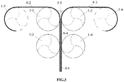
- a protective film A (9-2), a semi-cured slurry (9-1), and a protective film B (9-3) in step 1 are rolled by using a single-wheeled roller A1 (1-1) and a single-wheeled roller A2 (1-2) of one first smooth-surface dual-roller rolling apparatus, to obtain a rough photoconversion sheet (9-4).
- the rough photoconversion sheet (9-4) is then rolled by using a single-wheeled roller A3 (1-3) and a single-wheeled roller A4 (1-4) of a second smooth-surface dual-roller rolling apparatus, to obtain a refined photoconversion sheet (9-5).
- a thickness of the rough photoconversion sheet is no more than 850 ⁇ m. Optimally, the thickness of the rough photoconversion sheet is 150 ⁇ m to 300 ⁇ m. A thickness of the refined photoconversion sheet is no more than 800 ⁇ m. Optimally, the thickness of the refined photoconversion sheet is 150 ⁇ m to 250 ⁇ m.
- a material of the protective film A and the protective film B in step 1 is polyester, polyolefin or polyether.
- a temperature in the roll-forming using a single group or multiple groups of dual rollers is 50°C to 120°C. Optimally, the temperature in the roll-forming is 80°C to 100°C.
- a temperature in the low-temperature freezing in step 2 is -5°C to -40°C.
- the temperature of freezing is -10°C to -20°C.
- the pseudo-cured photoconversion sheet in step 2 means that the semi-cured photoconversion sheet obtained in step 1 is only physically hardened.
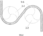
- step 2 the photoconversion sheet obtained in step 1 is pseudo-cured by using a first freezing single-wheeled roller (2-1) and a second freezing single-wheeled roller (2-2) of a freezing part with a temperature of -5°C to -40°C, to obtain a pseudo-cured photoconversion sheet (9-6).
- the carrier film in step 3 is a stretchable carrier film, and a material of the stretchable carrier film is high-temperature resistant polyester, polydimethylsiloxane or polyvinyl chloride.
- a temperature for enabling the pseudo-cured photoconversion sheet to turn from a pseudo-cured state to a semi-cured state by means of heating or/and illumination in step 4 is 50°C to 120°C.
- the temperature is 80°C to 100°C.
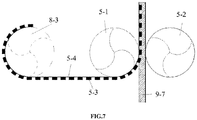
- step 4 for the pseudo-cured photoconversion sheet (9-6) obtained in step 2, the protective film B (9-3) is first removed by using a first traction single-wheeled roller (3-1) and a second traction single-wheeled roller (3-2) of a traction part.
- the removed protective film B (9-3) is received in a film-collecting roller (8-1).
- FIG. 5 shows that, as shown in FIG. 5 , in step 4, for the pseudo-cured photoconversion sheet (9-6) obtained in step 2, the protective film B (9-3) is first removed by using a first traction single-wheeled roller (3-1) and a second traction single-wheeled roller (3-2) of a traction part.
- the removed protective film B (9-3) is received in a film-collecting roller (8-1).
- the pseudo-cured photoconversion sheet is then turned from a pseudo-cured state to a semi-cured state by means of warming using a first rewarming single-wheeled roller (4-1) and a second rewarming single-wheeled roller (4-2) of a rewarming part, to obtain a semi-cured photoconversion sheet (9-7) with the protective film B removed.
- a bonding temperature in the forming by dual-roller roll-bonding is 50°C to 120°C.
- the temperature forming by bonding is 80°C to 100°C.
- step 4 the semi-cured photoconversion sheet (9-7) with the protective film B removed and the flip chip LED array sheet obtained in step 3 are rolled face-to-face in alignment with each other by using a first smooth-surface bonding single-wheeled roller (5-1) of a third dual-roller rolling apparatus and a second smooth-surface bonding single-wheeled roller (5-2) of the third dual-roller rolling apparatus, such that the flip chips LED in the flip chip LED array are bonded to and inserted in the semi-cured photoconversion sheet (9-7), to obtain the LED package elements.
- a first smooth-surface bonding single-wheeled roller (5-1) of a third dual-roller rolling apparatus and a second smooth-surface bonding single-wheeled roller (5-2) of the third dual-roller rolling apparatus, such that the flip chips LED in the flip chip LED array are bonded to and inserted in the semi-cured photoconversion sheet (9-7), to obtain the LED package elements.
- the photocuring in step 5 is curing with an active energy ray.
- a curing temperature is 140°C to 180°C, and a curing time is greater than or equal to 1 h.
- the curing temperature is 150°C to 160°C, and the curing time is 2 h.
- Step 6 of cutting the cured LED package elements means performing roll-cutting on the cured LED package elements by using an apparatus that includes a rolling piece A with an array cutter and a smooth-surface rolling piece B, to obtain the finished LED package elements having slits for splitting into single LED package elements.
- the rolling piece A with an array cutter is a single-wheeled roller A with an array cutter or a planar conveyor A with an array cutter
- the smooth-surface rolling piece B is a smooth-surface single-wheeled roller B or a smooth-surface planar conveyor B
- at least one of the rolling piece A with an array cutter and the smooth-surface rolling piece B is a single-wheeled roller.
- the array cutter in the rolling piece A with an array cutter is a cutter with an array of rectangular grids, where dimensions of the rectangular grid are the same as those of single finished LED package elements.
- An interval between single-wheeled rollers or between a single-wheeled roller and a planar conveyor does exceed a thickness of the carrier film in the flip chip LED array sheet.
- the slit in step 6 has a width no more than 20 ⁇ m. Optimally, the width of the slit is 15 ⁇ m.
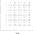
- the carrier films of the finished LED package elements are then stretched by using a stretcher, such that the finished LED package elements are split along the slits after being stretched, to obtain the single finished LED package elements, as shown in FIG. 8A and FIG. 8B .
- the process for bond-packaging an LED using an organic silicone resin photoconverter by tandem rolling provided in the present invention is widely applicable to processes of bond-packaging flip chip LEDs with various power using an organic silicone resin photoconverter.
- An equipment system used for the process for bond-packaging an LED using an organic silicone resin photoconverter by tandem rolling includes a protective film removing apparatus used to remove a protective film on one side of a photoconversion sheet with protective films on both sides and a roll-bonding apparatus that packages a reverse LED chip array by using the photoconversion sheet containing a protective film on a single side to form LED package elements.
- the protective film removing apparatus includes a photoconversion sheet freezing part, a traction part for pulling and removing a protective film on a single side of the frozen photoconversion sheet, and a photoconversion sheet rewarming part that are sequentially connected and disposed.
- the roll-bonding apparatus includes two smooth-surface bonding single-wheeled rollers whose rolling surfaces are both smooth surfaces.
- the photoconversion freezing sheet part is a freezing roller component.
- the freezing roller component includes one or more freezing single-wheeled rollers with a roller temperature of -40°C to -5°C.
- the photoconversion sheet freezing part in the protective film removing apparatus includes a first freezing single-wheeled roller (2-1) and a second freezing single-wheeled roller (2-2) with a temperature of -5°C to -40°C, and performs pseudo curing, to obtain a pseudo-cured photoconversion sheet (9-6).
- the photoconversion sheet freezing part is a temperature control device that includes a photoconversion sheet receiving port and a photoconversion sheet output port and sets an environmental temperature to -40°C to -5°C.
- the traction part includes a traction single-wheeled roller with clamping grooves.
- the clamping groove is used to fix the protective film on a single side of the photoconversion sheet. Holes matching the clamping grooves of the single-wheeled roller with the clamping grooves are provided on two sides in a width direction of the protective film on a single side.
- the protective film removing apparatus further includes a film collector. Referring to FIG. 5 , the traction part for a protective film on a single side includes a first traction single-wheeled roller (3-1) and a second traction single-wheeled roller (3-2) with clamping grooves, and removes a protective film B (9-3). The removed protective film B (9-3) is received in a film-collecting roller (8-1).
- the photoconversion sheet rewarming part is a heating roller component.
- the heating roller component includes one or more rewarming single-wheeled rollers with a roller temperature of 50°C to 120°C.
- the photoconversion sheet rewarming part is a temperature control device that is provided with a photoconversion sheet receiving port and a photoconversion sheet output port and sets an environmental temperature to 50°C to 120°C.
- the photoconversion sheet rewarming part includes a first rewarming single-wheeled roller (4-1) and a second rewarming single-wheeled roller (4-2).
- the pseudo-cured photoconversion sheet is turned from a pseudo-cured state to a semi-cured state by means of warming, to obtain a semi-cured photoconversion sheet (9-7) with the protective film B removed.
- the two single-wheeled rollers whose rolling surfaces are both smooth surfaces in the roll-bonding apparatus refer to a single-wheeled roller arranged with the photoconversion sheet and a single-wheeled roller arranged with the flip chip LED array sheet, the single-wheeled rollers being disposed face-to-face in alignment with each other.
- the roll-bonding apparatus is a third dual-roller rolling apparatus, and includes a first smooth-surface bonding single-wheeled roller (5-1) and a second smooth-surface bonding single-wheeled roller (5-2) that perform rolling face-to-face in alignment with each other.
- the semi-cured photoconversion sheet (9-7) with the protective film B removed and the flip chip LED array sheet pass through the dual-roller rolling apparatus, such that the flip chip LEDs in the flip chip LED array are bonded to and inserted in the semi-cured photoconversion sheet (9-7), to obtain the LED package elements.
- a displacement adjusting apparatus for adjusting a roller interval between the single-wheeled roller for the photoconversion sheet and the single-wheeled roller for the flip chip LED array sheet is provided for the two single-wheeled rollers whose rolling surfaces are both smooth surfaces. Radial run-out distances of the single-wheeled roller arranged with the photoconversion sheet and the single-wheeled roller arranged with the flip chip LED array sheet are both less than or equal to 2 ⁇ m.
- the equipment system further includes a roll-laminating apparatus for manufacturing a photoconversion sheet.
- the roll-laminating apparatus is a process apparatus located at a front end of the protective film removing apparatus.
- the roll-laminating apparatus includes one or more groups of dual rollers.
- the roll-laminating apparatus includes a first smooth-surface dual-roller rolling apparatus and a second smooth-surface dual-roller rolling apparatus.
- the first smooth-surface dual-roller rolling apparatus includes a single-wheeled roller A1 (1-1) and a single-wheeled roller A2 (1-2).
- the second smooth-surface dual-roller rolling apparatus includes a single-wheeled roller A3 (1-3) and a single-wheeled roller A4 (1-4).
- a protective film A (9-2), a semi-cured slurry (9-1), and a protective film B (9-3) are rolled by using the single-wheeled roller A1 (1-1) and the single-wheeled roller A2 (1-2), to obtain a rough photoconversion sheet (9-4).
- the rough photoconversion sheet (9-4) is then rolled by using the single-wheeled roller A3 (1-3) and the single-wheeled roller A4 (1-4), to obtain a refined photoconversion sheet (9-5).
- the equipment system further includes a curing apparatus.
- the curing apparatus is a process apparatus located at a rear end of the roll-bonding apparatus.
- the curing apparatus is a tunnel-type temperature control apparatus or a tunnel-type illumination apparatus.
- the tunnel-type temperature control apparatus includes a warming part, a temperature regulation part, and a conveyor belt passage.
- the tunnel-type illumination apparatus includes an illumination part, a light intensity regulation part, and a conveyor belt passage.
- the equipment system further includes a cutting apparatus for cutting the cured LED package elements.
- the cutting apparatus is process equipment disposed at a rear end of the curing apparatus.
- the cutting apparatus is a roll cutting apparatus.
- the roll cutting apparatus includes a rolling piece A with an array cutter and a smooth-surface rolling piece B disposed face-to-face in alignment with each other.
- the rolling piece A with an array cutter in the roll cutting apparatus is a single-wheeled roller A with an array cutter or a planar conveyor A with an array cutter.
- the smooth-surface rolling piece B is a smooth-surface single-wheeled roller B or a smooth-surface planar conveyor B. At least one of the rolling piece A with an array cutter and the smooth-surface rolling piece B is a single-wheeled roller.
- the array cutter is a cutter with an array of rectangular grids. Dimensions of the rectangular grid are the same as those of single LED package elements.
- the roll cutting apparatus is provided with a displacement adjusting apparatus for adjusting an interval between the rolling piece A with an array cutter and the smooth-surface rolling piece B.
- a roller radial run-out distance of a single-wheeled roller which is either the rolling piece A with an array cutter or the smooth-surface rolling piece B, is less than or equal to 2 ⁇ m.
- the present invention gains a satisfactory trial result after repeated test and verification.
Landscapes
- Led Device Packages (AREA)
- Casting Or Compression Moulding Of Plastics Or The Like (AREA)
- Encapsulation Of And Coatings For Semiconductor Or Solid State Devices (AREA)
- Engineering & Computer Science (AREA)
- Microelectronics & Electronic Packaging (AREA)
Priority Applications (1)
| Application Number | Priority Date | Filing Date | Title |
|---|---|---|---|
| PL15901631T PL3340320T3 (pl) | 2015-08-18 | 2015-12-18 | Metoda procesowa z wykorzystaniem fotokonwertera żywicy organicznej do pakietu dodatkowego led przez rolkowanie tandemowe |
Applications Claiming Priority (2)
| Application Number | Priority Date | Filing Date | Title |
|---|---|---|---|
| CN201510509581.6A CN106469780B (zh) | 2015-08-18 | 2015-08-18 | 一种基于串联滚压的有机硅树脂光转换体贴合封装led的工艺方法 |
| PCT/CN2015/097906 WO2017028429A1 (zh) | 2015-08-18 | 2015-12-18 | 一种基于串联滚压的有机硅树脂光转换体贴合封装led的工艺方法 |
Publications (3)
| Publication Number | Publication Date |
|---|---|
| EP3340320A1 true EP3340320A1 (de) | 2018-06-27 |
| EP3340320A4 EP3340320A4 (de) | 2018-08-01 |
| EP3340320B1 EP3340320B1 (de) | 2019-08-21 |
Family
ID=58050699
Family Applications (1)
| Application Number | Title | Priority Date | Filing Date |
|---|---|---|---|
| EP15901631.0A Active EP3340320B1 (de) | 2015-08-18 | 2015-12-18 | Prozessverfahren unter verwendung eines organischen silikonharz photokonverters zur bond-verpackung einer led durch tandemwalzen |
Country Status (7)
| Country | Link |
|---|---|
| US (1) | US10141486B2 (de) |
| EP (1) | EP3340320B1 (de) |
| JP (1) | JP6675423B2 (de) |
| KR (1) | KR102026842B1 (de) |
| CN (1) | CN106469780B (de) |
| PL (1) | PL3340320T3 (de) |
| WO (1) | WO2017028429A1 (de) |
Families Citing this family (3)
| Publication number | Priority date | Publication date | Assignee | Title |
|---|---|---|---|---|
| CN106469780B (zh) | 2015-08-18 | 2018-02-13 | 江苏诚睿达光电有限公司 | 一种基于串联滚压的有机硅树脂光转换体贴合封装led的工艺方法 |
| WO2018030695A1 (ko) * | 2016-08-11 | 2018-02-15 | 주식회사 루멘스 | 엘이디 모듈 및 그 제조방법 |
| WO2025181008A1 (en) * | 2024-03-01 | 2025-09-04 | Ams-Osram International Gmbh | Method of producing an optoelectronic component and optoelectronic component |
Family Cites Families (41)
| Publication number | Priority date | Publication date | Assignee | Title |
|---|---|---|---|---|
| JPH01174434A (ja) * | 1987-12-28 | 1989-07-11 | Chiharu Yoshihara | 板状体の製造法および装置 |
| JP2873842B2 (ja) * | 1989-12-07 | 1999-03-24 | 三菱レイヨン株式会社 | フイルム状熱硬化性樹脂の製造方法 |
| US5255431A (en) * | 1992-06-26 | 1993-10-26 | General Electric Company | Method of using frozen epoxy for placing pin-mounted components in a circuit module |
| US20050008821A1 (en) * | 2003-07-07 | 2005-01-13 | Pricone Robert M. | Process and apparatus for fabricating precise microstructures and polymeric molds for making same |
| US20070090387A1 (en) * | 2004-03-29 | 2007-04-26 | Articulated Technologies, Llc | Solid state light sheet and encapsulated bare die semiconductor circuits |
| US7259030B2 (en) * | 2004-03-29 | 2007-08-21 | Articulated Technologies, Llc | Roll-to-roll fabricated light sheet and encapsulated semiconductor circuit devices |
| US7591863B2 (en) | 2004-07-16 | 2009-09-22 | Semiconductor Energy Laboratory Co., Ltd. | Laminating system, IC sheet, roll of IC sheet, and method for manufacturing IC chip |
| JP4749062B2 (ja) | 2004-07-16 | 2011-08-17 | 株式会社半導体エネルギー研究所 | 薄膜集積回路を封止する装置及びicチップの作製方法 |
| JP4749074B2 (ja) * | 2004-07-30 | 2011-08-17 | 株式会社半導体エネルギー研究所 | Icチップの作製方法及び装置 |
| KR101254277B1 (ko) * | 2004-07-30 | 2013-04-15 | 가부시키가이샤 한도오따이 에네루기 켄큐쇼 | 라미네이팅 시스템, ic 시트, ic 시트 두루마리, 및ic 칩의 제조방법 |
| JP4676735B2 (ja) * | 2004-09-22 | 2011-04-27 | 東レ・ダウコーニング株式会社 | 光半導体装置の製造方法および光半導体装置 |
| US20060280912A1 (en) * | 2005-06-13 | 2006-12-14 | Rong-Chang Liang | Non-random array anisotropic conductive film (ACF) and manufacturing processes |
| US20080265462A1 (en) * | 2007-04-24 | 2008-10-30 | Advanced Chip Engineering Technology Inc. | Panel/wafer molding apparatus and method of the same |
| CN101306565A (zh) * | 2007-05-16 | 2008-11-19 | 鑫昌机械工业股份有限公司 | 亲油性橡胶薄制品压延生产方法 |
| JP5080881B2 (ja) * | 2007-06-27 | 2012-11-21 | ナミックス株式会社 | 発光ダイオードチップの封止体の製造方法 |
| CN101836032B (zh) * | 2007-10-22 | 2014-07-02 | 株式会社爱姆克鲁 | 面发光体和装入该面发光体而成的内照式广告牌 |
| JP2009194064A (ja) * | 2008-02-13 | 2009-08-27 | Takatori Corp | 基板への接着フィルム貼付け装置及び貼付け方法 |
| JP5064278B2 (ja) * | 2008-03-25 | 2012-10-31 | 日東電工株式会社 | 光半導体素子封止用樹脂シートおよび光半導体装置 |
| JP5093049B2 (ja) * | 2008-10-27 | 2012-12-05 | コニカミノルタホールディングス株式会社 | 有機エレクトロニクス素子、その製造方法、及び製造装置 |
| CN101901740B (zh) * | 2009-05-27 | 2011-10-19 | 台湾暹劲股份有限公司 | 一种电子元件切割剥料机及其方法 |
| CN105047597B (zh) * | 2009-06-15 | 2018-04-03 | 日东电工株式会社 | 半导体背面用切割带集成膜 |
| WO2011105185A1 (ja) | 2010-02-26 | 2011-09-01 | コニカミノルタオプト株式会社 | 光学半導体素子モジュールの製造方法 |
| CN101872828B (zh) | 2010-06-21 | 2012-07-25 | 深圳雷曼光电科技股份有限公司 | 一种倒装led芯片的封装方法 |
| TW201216526A (en) * | 2010-08-20 | 2012-04-16 | Koninkl Philips Electronics Nv | Lamination process for LEDs |
| JP2012142364A (ja) * | 2010-12-28 | 2012-07-26 | Nitto Denko Corp | 封止部材、封止方法、および、光半導体装置の製造方法 |
| KR20120081809A (ko) * | 2011-01-12 | 2012-07-20 | 삼성엘이디 주식회사 | 형광체 도포 방법 및 형광체 도포 장치 |
| KR20120109737A (ko) * | 2011-03-25 | 2012-10-09 | 삼성전자주식회사 | 발광 소자 패키지 및 그 제조 방법 |
| KR101769356B1 (ko) * | 2011-03-25 | 2017-08-18 | 삼성전자주식회사 | 발광소자에 형광체층을 형성하는 방법 및 장치 |
| CN102881780B (zh) * | 2011-07-15 | 2015-04-01 | 展晶科技(深圳)有限公司 | 发光模组及其制造方法 |
| JP2013183089A (ja) * | 2012-03-02 | 2013-09-12 | Idec Corp | 発光装置、照明装置、発光装置集合体および発光装置の製造方法 |
| KR20130100724A (ko) * | 2012-03-02 | 2013-09-11 | 닛토덴코 가부시키가이샤 | 발광 장치 집합체 및 조명 장치 |
| WO2013154602A1 (en) * | 2012-04-12 | 2013-10-17 | Saint-Gobain Performance Plastics Corporation | Method of manufacturing light emitting device |
| WO2014002784A1 (ja) * | 2012-06-28 | 2014-01-03 | 東レ株式会社 | 樹脂シート積層体およびそれを用いた半導体発光素子の製造方法 |
| US20140001949A1 (en) * | 2012-06-29 | 2014-01-02 | Nitto Denko Corporation | Phosphor layer-covered led, producing method thereof, and led device |
| CN104396344A (zh) * | 2012-10-29 | 2015-03-04 | 日东电工株式会社 | 使用了卷对卷方式的有机电致发光面板的制造方法 |
| JP2014093403A (ja) * | 2012-11-02 | 2014-05-19 | Shin Etsu Chem Co Ltd | 熱硬化性シリコーン樹脂シート及びその製造方法、該熱硬化性シリコーン樹脂シートを使用する発光装置及びその製造方法 |
| JP5961148B2 (ja) * | 2013-08-02 | 2016-08-02 | 富士フイルム株式会社 | 発光装置の製造方法 |
| JP2015082580A (ja) * | 2013-10-23 | 2015-04-27 | 日東電工株式会社 | 半導体装置およびその製造方法 |
| CN106469778B (zh) * | 2015-08-18 | 2017-12-22 | 江苏诚睿达光电有限公司 | 一种异形有机硅树脂光转换体贴合封装led的工艺方法 |
| CN106469767B (zh) * | 2015-08-18 | 2017-12-01 | 江苏诚睿达光电有限公司 | 一种基于串联滚压的有机硅树脂光转换体贴合封装led的装备系统 |
| CN106469780B (zh) | 2015-08-18 | 2018-02-13 | 江苏诚睿达光电有限公司 | 一种基于串联滚压的有机硅树脂光转换体贴合封装led的工艺方法 |
-
2015
- 2015-08-18 CN CN201510509581.6A patent/CN106469780B/zh active Active
- 2015-12-18 EP EP15901631.0A patent/EP3340320B1/de active Active
- 2015-12-18 WO PCT/CN2015/097906 patent/WO2017028429A1/zh not_active Ceased
- 2015-12-18 JP JP2017567798A patent/JP6675423B2/ja active Active
- 2015-12-18 KR KR1020187002436A patent/KR102026842B1/ko active Active
- 2015-12-18 US US15/750,958 patent/US10141486B2/en active Active
- 2015-12-18 PL PL15901631T patent/PL3340320T3/pl unknown
Also Published As
| Publication number | Publication date |
|---|---|
| US10141486B2 (en) | 2018-11-27 |
| KR20180022862A (ko) | 2018-03-06 |
| EP3340320B1 (de) | 2019-08-21 |
| KR102026842B1 (ko) | 2019-09-30 |
| JP6675423B2 (ja) | 2020-04-01 |
| CN106469780B (zh) | 2018-02-13 |
| EP3340320A4 (de) | 2018-08-01 |
| CN106469780A (zh) | 2017-03-01 |
| JP2018525816A (ja) | 2018-09-06 |
| WO2017028429A1 (zh) | 2017-02-23 |
| PL3340320T3 (pl) | 2020-03-31 |
| US20180240947A1 (en) | 2018-08-23 |
Similar Documents
| Publication | Publication Date | Title |
|---|---|---|
| US10158051B2 (en) | Process method for refining photoconverter to bond-package LED and refinement equipment system | |
| US10546980B2 (en) | Process method using thermoplastic resin photoconverter to bond-package LED by rolling | |
| EP3340320B1 (de) | Prozessverfahren unter verwendung eines organischen silikonharz photokonverters zur bond-verpackung einer led durch tandemwalzen | |
| EP3316320B1 (de) | Ausrüstungssystem mit verwendung eines photokonverters aus organischem silikonharz zur bond-verpackung einer led durch tandemwalzen | |
| EP3340321B1 (de) | Prozessverfahren mit photokonverter aus verformbarem organischem silikonharz zur bond-verpackung einer led | |
| EP3321980B1 (de) | Ausrüstungssystem mit verwendung eines lichtwandlers aus verformbarem organischem silikonharz zur bond-verkapselung einer led | |
| EP3340319B1 (de) | Anlagensystem mit verwendung eines fotokonverters aus thermoplastischem harz zur bond-verpackung einer led durch walzen |
Legal Events
| Date | Code | Title | Description |
|---|---|---|---|
| STAA | Information on the status of an ep patent application or granted ep patent |
Free format text: STATUS: THE INTERNATIONAL PUBLICATION HAS BEEN MADE |
|
| PUAI | Public reference made under article 153(3) epc to a published international application that has entered the european phase |
Free format text: ORIGINAL CODE: 0009012 |
|
| STAA | Information on the status of an ep patent application or granted ep patent |
Free format text: STATUS: REQUEST FOR EXAMINATION WAS MADE |
|
| 17P | Request for examination filed |
Effective date: 20180208 |
|
| AK | Designated contracting states |
Kind code of ref document: A1 Designated state(s): AL AT BE BG CH CY CZ DE DK EE ES FI FR GB GR HR HU IE IS IT LI LT LU LV MC MK MT NL NO PL PT RO RS SE SI SK SM TR |
|
| AX | Request for extension of the european patent |
Extension state: BA ME |
|
| A4 | Supplementary search report drawn up and despatched |
Effective date: 20180703 |
|
| RIC1 | Information provided on ipc code assigned before grant |
Ipc: H01L 33/48 20100101ALI20180627BHEP Ipc: H01L 25/075 20060101ALI20180627BHEP Ipc: H01L 33/50 20100101AFI20180627BHEP |
|
| DAV | Request for validation of the european patent (deleted) | ||
| DAX | Request for extension of the european patent (deleted) | ||
| GRAP | Despatch of communication of intention to grant a patent |
Free format text: ORIGINAL CODE: EPIDOSNIGR1 |
|
| STAA | Information on the status of an ep patent application or granted ep patent |
Free format text: STATUS: GRANT OF PATENT IS INTENDED |
|
| INTG | Intention to grant announced |
Effective date: 20190529 |
|
| GRAS | Grant fee paid |
Free format text: ORIGINAL CODE: EPIDOSNIGR3 |
|
| GRAA | (expected) grant |
Free format text: ORIGINAL CODE: 0009210 |
|
| STAA | Information on the status of an ep patent application or granted ep patent |
Free format text: STATUS: THE PATENT HAS BEEN GRANTED |
|
| AK | Designated contracting states |
Kind code of ref document: B1 Designated state(s): AL AT BE BG CH CY CZ DE DK EE ES FI FR GB GR HR HU IE IS IT LI LT LU LV MC MK MT NL NO PL PT RO RS SE SI SK SM TR |
|
| REG | Reference to a national code |
Ref country code: GB Ref legal event code: FG4D |
|
| REG | Reference to a national code |
Ref country code: CH Ref legal event code: EP |
|
| REG | Reference to a national code |
Ref country code: DE Ref legal event code: R096 Ref document number: 602015036525 Country of ref document: DE |
|
| REG | Reference to a national code |
Ref country code: AT Ref legal event code: REF Ref document number: 1170750 Country of ref document: AT Kind code of ref document: T Effective date: 20190915 |
|
| REG | Reference to a national code |
Ref country code: IE Ref legal event code: FG4D |
|
| REG | Reference to a national code |
Ref country code: NL Ref legal event code: FP |
|
| REG | Reference to a national code |
Ref country code: LT Ref legal event code: MG4D |
|
| PG25 | Lapsed in a contracting state [announced via postgrant information from national office to epo] |
Ref country code: NO Free format text: LAPSE BECAUSE OF FAILURE TO SUBMIT A TRANSLATION OF THE DESCRIPTION OR TO PAY THE FEE WITHIN THE PRESCRIBED TIME-LIMIT Effective date: 20191121 Ref country code: PT Free format text: LAPSE BECAUSE OF FAILURE TO SUBMIT A TRANSLATION OF THE DESCRIPTION OR TO PAY THE FEE WITHIN THE PRESCRIBED TIME-LIMIT Effective date: 20191223 Ref country code: SE Free format text: LAPSE BECAUSE OF FAILURE TO SUBMIT A TRANSLATION OF THE DESCRIPTION OR TO PAY THE FEE WITHIN THE PRESCRIBED TIME-LIMIT Effective date: 20190821 Ref country code: FI Free format text: LAPSE BECAUSE OF FAILURE TO SUBMIT A TRANSLATION OF THE DESCRIPTION OR TO PAY THE FEE WITHIN THE PRESCRIBED TIME-LIMIT Effective date: 20190821 Ref country code: HR Free format text: LAPSE BECAUSE OF FAILURE TO SUBMIT A TRANSLATION OF THE DESCRIPTION OR TO PAY THE FEE WITHIN THE PRESCRIBED TIME-LIMIT Effective date: 20190821 Ref country code: LT Free format text: LAPSE BECAUSE OF FAILURE TO SUBMIT A TRANSLATION OF THE DESCRIPTION OR TO PAY THE FEE WITHIN THE PRESCRIBED TIME-LIMIT Effective date: 20190821 Ref country code: BG Free format text: LAPSE BECAUSE OF FAILURE TO SUBMIT A TRANSLATION OF THE DESCRIPTION OR TO PAY THE FEE WITHIN THE PRESCRIBED TIME-LIMIT Effective date: 20191121 |
|
| PG25 | Lapsed in a contracting state [announced via postgrant information from national office to epo] |
Ref country code: AL Free format text: LAPSE BECAUSE OF FAILURE TO SUBMIT A TRANSLATION OF THE DESCRIPTION OR TO PAY THE FEE WITHIN THE PRESCRIBED TIME-LIMIT Effective date: 20190821 Ref country code: ES Free format text: LAPSE BECAUSE OF FAILURE TO SUBMIT A TRANSLATION OF THE DESCRIPTION OR TO PAY THE FEE WITHIN THE PRESCRIBED TIME-LIMIT Effective date: 20190821 Ref country code: GR Free format text: LAPSE BECAUSE OF FAILURE TO SUBMIT A TRANSLATION OF THE DESCRIPTION OR TO PAY THE FEE WITHIN THE PRESCRIBED TIME-LIMIT Effective date: 20191122 Ref country code: LV Free format text: LAPSE BECAUSE OF FAILURE TO SUBMIT A TRANSLATION OF THE DESCRIPTION OR TO PAY THE FEE WITHIN THE PRESCRIBED TIME-LIMIT Effective date: 20190821 Ref country code: RS Free format text: LAPSE BECAUSE OF FAILURE TO SUBMIT A TRANSLATION OF THE DESCRIPTION OR TO PAY THE FEE WITHIN THE PRESCRIBED TIME-LIMIT Effective date: 20190821 Ref country code: IS Free format text: LAPSE BECAUSE OF FAILURE TO SUBMIT A TRANSLATION OF THE DESCRIPTION OR TO PAY THE FEE WITHIN THE PRESCRIBED TIME-LIMIT Effective date: 20191221 |
|
| REG | Reference to a national code |
Ref country code: AT Ref legal event code: MK05 Ref document number: 1170750 Country of ref document: AT Kind code of ref document: T Effective date: 20190821 |
|
| PG25 | Lapsed in a contracting state [announced via postgrant information from national office to epo] |
Ref country code: TR Free format text: LAPSE BECAUSE OF FAILURE TO SUBMIT A TRANSLATION OF THE DESCRIPTION OR TO PAY THE FEE WITHIN THE PRESCRIBED TIME-LIMIT Effective date: 20190821 |
|
| PG25 | Lapsed in a contracting state [announced via postgrant information from national office to epo] |
Ref country code: RO Free format text: LAPSE BECAUSE OF FAILURE TO SUBMIT A TRANSLATION OF THE DESCRIPTION OR TO PAY THE FEE WITHIN THE PRESCRIBED TIME-LIMIT Effective date: 20190821 Ref country code: EE Free format text: LAPSE BECAUSE OF FAILURE TO SUBMIT A TRANSLATION OF THE DESCRIPTION OR TO PAY THE FEE WITHIN THE PRESCRIBED TIME-LIMIT Effective date: 20190821 Ref country code: AT Free format text: LAPSE BECAUSE OF FAILURE TO SUBMIT A TRANSLATION OF THE DESCRIPTION OR TO PAY THE FEE WITHIN THE PRESCRIBED TIME-LIMIT Effective date: 20190821 Ref country code: IT Free format text: LAPSE BECAUSE OF FAILURE TO SUBMIT A TRANSLATION OF THE DESCRIPTION OR TO PAY THE FEE WITHIN THE PRESCRIBED TIME-LIMIT Effective date: 20190821 Ref country code: DK Free format text: LAPSE BECAUSE OF FAILURE TO SUBMIT A TRANSLATION OF THE DESCRIPTION OR TO PAY THE FEE WITHIN THE PRESCRIBED TIME-LIMIT Effective date: 20190821 |
|
| PG25 | Lapsed in a contracting state [announced via postgrant information from national office to epo] |
Ref country code: IS Free format text: LAPSE BECAUSE OF FAILURE TO SUBMIT A TRANSLATION OF THE DESCRIPTION OR TO PAY THE FEE WITHIN THE PRESCRIBED TIME-LIMIT Effective date: 20200224 Ref country code: CZ Free format text: LAPSE BECAUSE OF FAILURE TO SUBMIT A TRANSLATION OF THE DESCRIPTION OR TO PAY THE FEE WITHIN THE PRESCRIBED TIME-LIMIT Effective date: 20190821 Ref country code: SM Free format text: LAPSE BECAUSE OF FAILURE TO SUBMIT A TRANSLATION OF THE DESCRIPTION OR TO PAY THE FEE WITHIN THE PRESCRIBED TIME-LIMIT Effective date: 20190821 Ref country code: SK Free format text: LAPSE BECAUSE OF FAILURE TO SUBMIT A TRANSLATION OF THE DESCRIPTION OR TO PAY THE FEE WITHIN THE PRESCRIBED TIME-LIMIT Effective date: 20190821 |
|
| REG | Reference to a national code |
Ref country code: DE Ref legal event code: R097 Ref document number: 602015036525 Country of ref document: DE |
|
| PLBE | No opposition filed within time limit |
Free format text: ORIGINAL CODE: 0009261 |
|
| STAA | Information on the status of an ep patent application or granted ep patent |
Free format text: STATUS: NO OPPOSITION FILED WITHIN TIME LIMIT |
|
| PG2D | Information on lapse in contracting state deleted |
Ref country code: IS |
|
| REG | Reference to a national code |
Ref country code: CH Ref legal event code: PL |
|
| 26N | No opposition filed |
Effective date: 20200603 |
|
| REG | Reference to a national code |
Ref country code: BE Ref legal event code: MM Effective date: 20191231 |
|
| PG25 | Lapsed in a contracting state [announced via postgrant information from national office to epo] |
Ref country code: MC Free format text: LAPSE BECAUSE OF FAILURE TO SUBMIT A TRANSLATION OF THE DESCRIPTION OR TO PAY THE FEE WITHIN THE PRESCRIBED TIME-LIMIT Effective date: 20190821 Ref country code: SI Free format text: LAPSE BECAUSE OF FAILURE TO SUBMIT A TRANSLATION OF THE DESCRIPTION OR TO PAY THE FEE WITHIN THE PRESCRIBED TIME-LIMIT Effective date: 20190821 |
|
| PG25 | Lapsed in a contracting state [announced via postgrant information from national office to epo] |
Ref country code: IE Free format text: LAPSE BECAUSE OF NON-PAYMENT OF DUE FEES Effective date: 20191218 Ref country code: LU Free format text: LAPSE BECAUSE OF NON-PAYMENT OF DUE FEES Effective date: 20191218 |
|
| PG25 | Lapsed in a contracting state [announced via postgrant information from national office to epo] |
Ref country code: CH Free format text: LAPSE BECAUSE OF NON-PAYMENT OF DUE FEES Effective date: 20191231 Ref country code: LI Free format text: LAPSE BECAUSE OF NON-PAYMENT OF DUE FEES Effective date: 20191231 Ref country code: BE Free format text: LAPSE BECAUSE OF NON-PAYMENT OF DUE FEES Effective date: 20191231 |
|
| PG25 | Lapsed in a contracting state [announced via postgrant information from national office to epo] |
Ref country code: CY Free format text: LAPSE BECAUSE OF FAILURE TO SUBMIT A TRANSLATION OF THE DESCRIPTION OR TO PAY THE FEE WITHIN THE PRESCRIBED TIME-LIMIT Effective date: 20190821 |
|
| PG25 | Lapsed in a contracting state [announced via postgrant information from national office to epo] |
Ref country code: MT Free format text: LAPSE BECAUSE OF FAILURE TO SUBMIT A TRANSLATION OF THE DESCRIPTION OR TO PAY THE FEE WITHIN THE PRESCRIBED TIME-LIMIT Effective date: 20190821 Ref country code: HU Free format text: LAPSE BECAUSE OF FAILURE TO SUBMIT A TRANSLATION OF THE DESCRIPTION OR TO PAY THE FEE WITHIN THE PRESCRIBED TIME-LIMIT; INVALID AB INITIO Effective date: 20151218 |
|
| PG25 | Lapsed in a contracting state [announced via postgrant information from national office to epo] |
Ref country code: MK Free format text: LAPSE BECAUSE OF FAILURE TO SUBMIT A TRANSLATION OF THE DESCRIPTION OR TO PAY THE FEE WITHIN THE PRESCRIBED TIME-LIMIT Effective date: 20190821 |
|
| REG | Reference to a national code |
Ref country code: DE Ref legal event code: R079 Ref document number: 602015036525 Country of ref document: DE Free format text: PREVIOUS MAIN CLASS: H01L0033500000 Ipc: H10H0020851000 |
|
| PGFP | Annual fee paid to national office [announced via postgrant information from national office to epo] |
Ref country code: NL Payment date: 20251127 Year of fee payment: 11 |
|
| PGFP | Annual fee paid to national office [announced via postgrant information from national office to epo] |
Ref country code: GB Payment date: 20251229 Year of fee payment: 11 |
|
| PGFP | Annual fee paid to national office [announced via postgrant information from national office to epo] |
Ref country code: FR Payment date: 20251230 Year of fee payment: 11 |
|
| PGFP | Annual fee paid to national office [announced via postgrant information from national office to epo] |
Ref country code: PL Payment date: 20251120 Year of fee payment: 11 |
|
| PGFP | Annual fee paid to national office [announced via postgrant information from national office to epo] |
Ref country code: DE Payment date: 20251231 Year of fee payment: 11 |