EP3343280A1 - Anzeigesubstrat - Google Patents
Anzeigesubstrat Download PDFInfo
- Publication number
- EP3343280A1 EP3343280A1 EP16760636.7A EP16760636A EP3343280A1 EP 3343280 A1 EP3343280 A1 EP 3343280A1 EP 16760636 A EP16760636 A EP 16760636A EP 3343280 A1 EP3343280 A1 EP 3343280A1
- Authority
- EP
- European Patent Office
- Prior art keywords
- layer
- display substrate
- quantum dot
- metal film
- light
- Prior art date
- Legal status (The legal status is an assumption and is not a legal conclusion. Google has not performed a legal analysis and makes no representation as to the accuracy of the status listed.)
- Withdrawn
Links
Images

Classifications
-
- G—PHYSICS
- G02—OPTICS
- G02F—OPTICAL DEVICES OR ARRANGEMENTS FOR THE CONTROL OF LIGHT BY MODIFICATION OF THE OPTICAL PROPERTIES OF THE MEDIA OF THE ELEMENTS INVOLVED THEREIN; NON-LINEAR OPTICS; FREQUENCY-CHANGING OF LIGHT; OPTICAL LOGIC ELEMENTS; OPTICAL ANALOGUE/DIGITAL CONVERTERS
- G02F1/00—Devices or arrangements for the control of the intensity, colour, phase, polarisation or direction of light arriving from an independent light source, e.g. switching, gating or modulating; Non-linear optics
- G02F1/01—Devices or arrangements for the control of the intensity, colour, phase, polarisation or direction of light arriving from an independent light source, e.g. switching, gating or modulating; Non-linear optics for the control of the intensity, phase, polarisation or colour
- G02F1/13—Devices or arrangements for the control of the intensity, colour, phase, polarisation or direction of light arriving from an independent light source, e.g. switching, gating or modulating; Non-linear optics for the control of the intensity, phase, polarisation or colour based on liquid crystals, e.g. single liquid crystal display cells
- G02F1/133—Constructional arrangements; Operation of liquid crystal cells; Circuit arrangements
- G02F1/1333—Constructional arrangements; Manufacturing methods
- G02F1/1335—Structural association of cells with optical devices, e.g. polarisers or reflectors
- G02F1/133509—Filters, e.g. light shielding masks
- G02F1/133514—Colour filters
- G02F1/133516—Methods for their manufacture, e.g. printing, electro-deposition or photolithography
-
- G—PHYSICS
- G02—OPTICS
- G02F—OPTICAL DEVICES OR ARRANGEMENTS FOR THE CONTROL OF LIGHT BY MODIFICATION OF THE OPTICAL PROPERTIES OF THE MEDIA OF THE ELEMENTS INVOLVED THEREIN; NON-LINEAR OPTICS; FREQUENCY-CHANGING OF LIGHT; OPTICAL LOGIC ELEMENTS; OPTICAL ANALOGUE/DIGITAL CONVERTERS
- G02F1/00—Devices or arrangements for the control of the intensity, colour, phase, polarisation or direction of light arriving from an independent light source, e.g. switching, gating or modulating; Non-linear optics
- G02F1/01—Devices or arrangements for the control of the intensity, colour, phase, polarisation or direction of light arriving from an independent light source, e.g. switching, gating or modulating; Non-linear optics for the control of the intensity, phase, polarisation or colour
- G02F1/13—Devices or arrangements for the control of the intensity, colour, phase, polarisation or direction of light arriving from an independent light source, e.g. switching, gating or modulating; Non-linear optics for the control of the intensity, phase, polarisation or colour based on liquid crystals, e.g. single liquid crystal display cells
- G02F1/133—Constructional arrangements; Operation of liquid crystal cells; Circuit arrangements
- G02F1/1333—Constructional arrangements; Manufacturing methods
- G02F1/1335—Structural association of cells with optical devices, e.g. polarisers or reflectors
- G02F1/133509—Filters, e.g. light shielding masks
- G02F1/133512—Light shielding layers, e.g. black matrix
-
- G—PHYSICS
- G02—OPTICS
- G02F—OPTICAL DEVICES OR ARRANGEMENTS FOR THE CONTROL OF LIGHT BY MODIFICATION OF THE OPTICAL PROPERTIES OF THE MEDIA OF THE ELEMENTS INVOLVED THEREIN; NON-LINEAR OPTICS; FREQUENCY-CHANGING OF LIGHT; OPTICAL LOGIC ELEMENTS; OPTICAL ANALOGUE/DIGITAL CONVERTERS
- G02F1/00—Devices or arrangements for the control of the intensity, colour, phase, polarisation or direction of light arriving from an independent light source, e.g. switching, gating or modulating; Non-linear optics
- G02F1/01—Devices or arrangements for the control of the intensity, colour, phase, polarisation or direction of light arriving from an independent light source, e.g. switching, gating or modulating; Non-linear optics for the control of the intensity, phase, polarisation or colour
- G02F1/13—Devices or arrangements for the control of the intensity, colour, phase, polarisation or direction of light arriving from an independent light source, e.g. switching, gating or modulating; Non-linear optics for the control of the intensity, phase, polarisation or colour based on liquid crystals, e.g. single liquid crystal display cells
- G02F1/133—Constructional arrangements; Operation of liquid crystal cells; Circuit arrangements
- G02F1/1333—Constructional arrangements; Manufacturing methods
- G02F1/1335—Structural association of cells with optical devices, e.g. polarisers or reflectors
- G02F1/133528—Polarisers
-
- G—PHYSICS
- G02—OPTICS
- G02B—OPTICAL ELEMENTS, SYSTEMS OR APPARATUS
- G02B5/00—Optical elements other than lenses
- G02B5/30—Polarising elements
- G02B5/3025—Polarisers, i.e. arrangements capable of producing a definite output polarisation state from an unpolarised input state
- G02B5/3058—Polarisers, i.e. arrangements capable of producing a definite output polarisation state from an unpolarised input state comprising electrically conductive elements, e.g. wire grids, conductive particles
-
- G—PHYSICS
- G02—OPTICS
- G02F—OPTICAL DEVICES OR ARRANGEMENTS FOR THE CONTROL OF LIGHT BY MODIFICATION OF THE OPTICAL PROPERTIES OF THE MEDIA OF THE ELEMENTS INVOLVED THEREIN; NON-LINEAR OPTICS; FREQUENCY-CHANGING OF LIGHT; OPTICAL LOGIC ELEMENTS; OPTICAL ANALOGUE/DIGITAL CONVERTERS
- G02F1/00—Devices or arrangements for the control of the intensity, colour, phase, polarisation or direction of light arriving from an independent light source, e.g. switching, gating or modulating; Non-linear optics
- G02F1/01—Devices or arrangements for the control of the intensity, colour, phase, polarisation or direction of light arriving from an independent light source, e.g. switching, gating or modulating; Non-linear optics for the control of the intensity, phase, polarisation or colour
- G02F1/13—Devices or arrangements for the control of the intensity, colour, phase, polarisation or direction of light arriving from an independent light source, e.g. switching, gating or modulating; Non-linear optics for the control of the intensity, phase, polarisation or colour based on liquid crystals, e.g. single liquid crystal display cells
- G02F1/133—Constructional arrangements; Operation of liquid crystal cells; Circuit arrangements
- G02F1/1333—Constructional arrangements; Manufacturing methods
- G02F1/1335—Structural association of cells with optical devices, e.g. polarisers or reflectors
- G02F1/1336—Illuminating devices
- G02F1/133617—Illumination with ultraviolet light; Luminescent elements or materials associated to the cell
-
- G—PHYSICS
- G02—OPTICS
- G02F—OPTICAL DEVICES OR ARRANGEMENTS FOR THE CONTROL OF LIGHT BY MODIFICATION OF THE OPTICAL PROPERTIES OF THE MEDIA OF THE ELEMENTS INVOLVED THEREIN; NON-LINEAR OPTICS; FREQUENCY-CHANGING OF LIGHT; OPTICAL LOGIC ELEMENTS; OPTICAL ANALOGUE/DIGITAL CONVERTERS
- G02F1/00—Devices or arrangements for the control of the intensity, colour, phase, polarisation or direction of light arriving from an independent light source, e.g. switching, gating or modulating; Non-linear optics
- G02F1/01—Devices or arrangements for the control of the intensity, colour, phase, polarisation or direction of light arriving from an independent light source, e.g. switching, gating or modulating; Non-linear optics for the control of the intensity, phase, polarisation or colour
- G02F1/13—Devices or arrangements for the control of the intensity, colour, phase, polarisation or direction of light arriving from an independent light source, e.g. switching, gating or modulating; Non-linear optics for the control of the intensity, phase, polarisation or colour based on liquid crystals, e.g. single liquid crystal display cells
- G02F1/133—Constructional arrangements; Operation of liquid crystal cells; Circuit arrangements
- G02F1/136—Liquid crystal cells structurally associated with a semi-conducting layer or substrate, e.g. cells forming part of an integrated circuit
- G02F1/1362—Active matrix addressed cells
- G02F1/136209—Light shielding layers, e.g. black matrix, incorporated in the active matrix substrate, e.g. structurally associated with the switching element
-
- G—PHYSICS
- G02—OPTICS
- G02F—OPTICAL DEVICES OR ARRANGEMENTS FOR THE CONTROL OF LIGHT BY MODIFICATION OF THE OPTICAL PROPERTIES OF THE MEDIA OF THE ELEMENTS INVOLVED THEREIN; NON-LINEAR OPTICS; FREQUENCY-CHANGING OF LIGHT; OPTICAL LOGIC ELEMENTS; OPTICAL ANALOGUE/DIGITAL CONVERTERS
- G02F1/00—Devices or arrangements for the control of the intensity, colour, phase, polarisation or direction of light arriving from an independent light source, e.g. switching, gating or modulating; Non-linear optics
- G02F1/01—Devices or arrangements for the control of the intensity, colour, phase, polarisation or direction of light arriving from an independent light source, e.g. switching, gating or modulating; Non-linear optics for the control of the intensity, phase, polarisation or colour
- G02F1/13—Devices or arrangements for the control of the intensity, colour, phase, polarisation or direction of light arriving from an independent light source, e.g. switching, gating or modulating; Non-linear optics for the control of the intensity, phase, polarisation or colour based on liquid crystals, e.g. single liquid crystal display cells
- G02F1/133—Constructional arrangements; Operation of liquid crystal cells; Circuit arrangements
- G02F1/136—Liquid crystal cells structurally associated with a semi-conducting layer or substrate, e.g. cells forming part of an integrated circuit
- G02F1/1362—Active matrix addressed cells
- G02F1/1368—Active matrix addressed cells in which the switching element is a three-electrode device
-
- G—PHYSICS
- G03—PHOTOGRAPHY; CINEMATOGRAPHY; ANALOGOUS TECHNIQUES USING WAVES OTHER THAN OPTICAL WAVES; ELECTROGRAPHY; HOLOGRAPHY
- G03F—PHOTOMECHANICAL PRODUCTION OF TEXTURED OR PATTERNED SURFACES, e.g. FOR PRINTING, FOR PROCESSING OF SEMICONDUCTOR DEVICES; MATERIALS THEREFOR; ORIGINALS THEREFOR; APPARATUS SPECIALLY ADAPTED THEREFOR
- G03F7/00—Photomechanical, e.g. photolithographic, production of textured or patterned surfaces, e.g. printing surfaces; Materials therefor, e.g. comprising photoresists; Apparatus specially adapted therefor
- G03F7/20—Exposure; Apparatus therefor
- G03F7/2041—Exposure; Apparatus therefor in the presence of a fluid, e.g. immersion; using fluid cooling means
- G03F7/2043—Exposure; Apparatus therefor in the presence of a fluid, e.g. immersion; using fluid cooling means with the production of a chemical active agent from a fluid, e.g. an etching agent; with meterial deposition from the fluid phase, e.g. contamination resists
-
- G—PHYSICS
- G02—OPTICS
- G02F—OPTICAL DEVICES OR ARRANGEMENTS FOR THE CONTROL OF LIGHT BY MODIFICATION OF THE OPTICAL PROPERTIES OF THE MEDIA OF THE ELEMENTS INVOLVED THEREIN; NON-LINEAR OPTICS; FREQUENCY-CHANGING OF LIGHT; OPTICAL LOGIC ELEMENTS; OPTICAL ANALOGUE/DIGITAL CONVERTERS
- G02F1/00—Devices or arrangements for the control of the intensity, colour, phase, polarisation or direction of light arriving from an independent light source, e.g. switching, gating or modulating; Non-linear optics
- G02F1/01—Devices or arrangements for the control of the intensity, colour, phase, polarisation or direction of light arriving from an independent light source, e.g. switching, gating or modulating; Non-linear optics for the control of the intensity, phase, polarisation or colour
- G02F1/13—Devices or arrangements for the control of the intensity, colour, phase, polarisation or direction of light arriving from an independent light source, e.g. switching, gating or modulating; Non-linear optics for the control of the intensity, phase, polarisation or colour based on liquid crystals, e.g. single liquid crystal display cells
- G02F1/133—Constructional arrangements; Operation of liquid crystal cells; Circuit arrangements
- G02F1/1333—Constructional arrangements; Manufacturing methods
- G02F1/133357—Planarisation layers
-
- G—PHYSICS
- G02—OPTICS
- G02F—OPTICAL DEVICES OR ARRANGEMENTS FOR THE CONTROL OF LIGHT BY MODIFICATION OF THE OPTICAL PROPERTIES OF THE MEDIA OF THE ELEMENTS INVOLVED THEREIN; NON-LINEAR OPTICS; FREQUENCY-CHANGING OF LIGHT; OPTICAL LOGIC ELEMENTS; OPTICAL ANALOGUE/DIGITAL CONVERTERS
- G02F1/00—Devices or arrangements for the control of the intensity, colour, phase, polarisation or direction of light arriving from an independent light source, e.g. switching, gating or modulating; Non-linear optics
- G02F1/01—Devices or arrangements for the control of the intensity, colour, phase, polarisation or direction of light arriving from an independent light source, e.g. switching, gating or modulating; Non-linear optics for the control of the intensity, phase, polarisation or colour
- G02F1/13—Devices or arrangements for the control of the intensity, colour, phase, polarisation or direction of light arriving from an independent light source, e.g. switching, gating or modulating; Non-linear optics for the control of the intensity, phase, polarisation or colour based on liquid crystals, e.g. single liquid crystal display cells
- G02F1/133—Constructional arrangements; Operation of liquid crystal cells; Circuit arrangements
- G02F1/1333—Constructional arrangements; Manufacturing methods
- G02F1/1335—Structural association of cells with optical devices, e.g. polarisers or reflectors
- G02F1/133528—Polarisers
- G02F1/133548—Wire-grid polarisers
-
- G—PHYSICS
- G02—OPTICS
- G02F—OPTICAL DEVICES OR ARRANGEMENTS FOR THE CONTROL OF LIGHT BY MODIFICATION OF THE OPTICAL PROPERTIES OF THE MEDIA OF THE ELEMENTS INVOLVED THEREIN; NON-LINEAR OPTICS; FREQUENCY-CHANGING OF LIGHT; OPTICAL LOGIC ELEMENTS; OPTICAL ANALOGUE/DIGITAL CONVERTERS
- G02F1/00—Devices or arrangements for the control of the intensity, colour, phase, polarisation or direction of light arriving from an independent light source, e.g. switching, gating or modulating; Non-linear optics
- G02F1/01—Devices or arrangements for the control of the intensity, colour, phase, polarisation or direction of light arriving from an independent light source, e.g. switching, gating or modulating; Non-linear optics for the control of the intensity, phase, polarisation or colour
- G02F1/13—Devices or arrangements for the control of the intensity, colour, phase, polarisation or direction of light arriving from an independent light source, e.g. switching, gating or modulating; Non-linear optics for the control of the intensity, phase, polarisation or colour based on liquid crystals, e.g. single liquid crystal display cells
- G02F1/133—Constructional arrangements; Operation of liquid crystal cells; Circuit arrangements
- G02F1/1333—Constructional arrangements; Manufacturing methods
- G02F1/1335—Structural association of cells with optical devices, e.g. polarisers or reflectors
- G02F1/1336—Illuminating devices
- G02F1/133614—Illuminating devices using photoluminescence, e.g. phosphors illuminated by UV or blue light
-
- G—PHYSICS
- G03—PHOTOGRAPHY; CINEMATOGRAPHY; ANALOGOUS TECHNIQUES USING WAVES OTHER THAN OPTICAL WAVES; ELECTROGRAPHY; HOLOGRAPHY
- G03F—PHOTOMECHANICAL PRODUCTION OF TEXTURED OR PATTERNED SURFACES, e.g. FOR PRINTING, FOR PROCESSING OF SEMICONDUCTOR DEVICES; MATERIALS THEREFOR; ORIGINALS THEREFOR; APPARATUS SPECIALLY ADAPTED THEREFOR
- G03F7/00—Photomechanical, e.g. photolithographic, production of textured or patterned surfaces, e.g. printing surfaces; Materials therefor, e.g. comprising photoresists; Apparatus specially adapted therefor
- G03F7/0002—Lithographic processes using patterning methods other than those involving the exposure to radiation, e.g. by stamping
-
- G—PHYSICS
- G03—PHOTOGRAPHY; CINEMATOGRAPHY; ANALOGOUS TECHNIQUES USING WAVES OTHER THAN OPTICAL WAVES; ELECTROGRAPHY; HOLOGRAPHY
- G03F—PHOTOMECHANICAL PRODUCTION OF TEXTURED OR PATTERNED SURFACES, e.g. FOR PRINTING, FOR PROCESSING OF SEMICONDUCTOR DEVICES; MATERIALS THEREFOR; ORIGINALS THEREFOR; APPARATUS SPECIALLY ADAPTED THEREFOR
- G03F7/00—Photomechanical, e.g. photolithographic, production of textured or patterned surfaces, e.g. printing surfaces; Materials therefor, e.g. comprising photoresists; Apparatus specially adapted therefor
- G03F7/0005—Production of optical devices or components in so far as characterised by the lithographic processes or materials used therefor
- G03F7/0007—Filters, e.g. additive colour filters; Components for display devices
Definitions
- the embodiment of the present invention relates to a display substrate.
- liquid crystal display In the conventional liquid crystal display (LCD), light-shielding matrixes and polarizers are generally formed in two independent layers, as a result, not only the production cost is increased but also the display device is thickened.
- Quantum dot materials have been used to manufacture a color filter (CF) substrate in an LCD device.
- Quantum dot is a semiconductor nanostructure for binding a conduction band electron, a valence band hole and an exciton in three spatial directions. The confinement can arise from electrostatic potential (generated by external electrodes, doping, strain, or impurities), interface of two different semiconductor materials (e.g., in self-assembled quantum dots), surface of semiconductors (e.g., semiconductor nanocrystals), or a combination thereof.
- Quantum dot is a nanoparticle formed by II-VI or III-V group elements. The particle diameter of the quantum dot is generally ranged from 1 to 10nm.
- quantum dots As electrons and holes are confined by quantum dots, continuous energy band structures become discrete energy band structures with molecular properties which can emit fluorescent light after excitation. Based on quantum effect, the quantum dot can be widely applied in the fields such as solar cells, luminescent devices and optical biomarkers.
- a white light-emitting diode (LED) backlight and conventional color filters (CFs) are generally matched with each other to form a color display light source which has the problems of low utilization rate, narrow color gamut of display, etc.
- CFs color filters
- the quantum dots are adopted as CF materials, the display color gamut can be effectively improved.
- Embodiments of the present invention provide a display substrate, comprising a base substrate and a polarization layer, wherein the polarization layer comprises grid polarizers (GPs) and light-shielding matrixes arranged in a same layer and made from a same material.
- GPs grid polarizers
- the display substrate is a color filter (CF) substrate; and the CF substrate further includes a quantum dot layer and a planarization layer disposed between the quantum dot layer and the polarization layer.
- CF color filter
- the display substrate is an array substrate which further includes thin-film transistors (TFTs) arranged in an array.
- TFTs thin-film transistors
- the GPs and the light-shielding matrixes in the polarization layer are made from a same metallic material.
- the metallic material is selected from the group consisting of: Al, Cu, Au, Ag and Cr.
- the planarization layer is made from resin materials containing polar bonds.
- the polar bonds are selected from the group consisting of: hydroxyl, carboxyl, carbonyl, ether bond, isocyanate group and urethano.
- the resin materials containing the polar bonds are selected from the group consisting of: epoxy resins, phenolic resins, urea resins, acrylic resins, polyvinyl alcohol, polyurethane, rubber, vinyl acetate and copolymers thereof, polystyrene and copolymers thereof, organo-silicon compounds and epoxy phenolic resins.
- an adhesive layer is disposed between the polarization layer and the planarization layer.
- a material of the adhesive layer includes at least one of indium tin oxide (ITO) and indium zinc oxide (IZO).
- a material of the quantum dot layer is selected from the group consisting of: CdS, CdSe, CdTe, ZnO, ZnS, ZnSe, ZnTe, GaAs, GaP, GaSb, HgS, HgSe, HgTe, InAs, InP, InSb, AlAs, AlP, CuInS, CuInSe and AlSb.
- the display substrate further comprising: spacers, wherein the spacers are arranged on one side of the display substrate opposite to the base substrate.
- the quantum dot layer includes a plurality of quantum dot CF units.
- Embodiments of the present invention provide a liquid crystal display (LCD) device comprising the above display substrate.
- LCD liquid crystal display
- Embodiments of the present invention provide a method for manufacturing a display substrate, comprising: providing a base substrate and depositing a metal film on the base substrate; and processing the metal film to form grid polarizers (GPs) and light-shielding matrixes.
- GPs grid polarizers
- the method comprising: providing the base substrate; forming a patterned quantum dot layer on the base substrate; forming a planarization layer on the patterned quantum dot layer; depositing the metal film on the planarization layer; and processing the metal film to form the GPs and light-shielding matrixes.
- processing the metal film to form the GPs and the light-shielding matrixes includes: coating photoresist on the metal film; impressing a mask on the photoresist to form a structure corresponding to the GPs and the light-shielding matrixes; demoulding and removing residual photoresist, and exposing the metal film; and etching the metal film and to form the GPs and the light-shielding matrixes.
- a material of the metal film is selected from the group consisting of Al, Cu, Au, Ag and Cr.
- a material of the adhesive layer is selected from ITO or IZO.
- Quantum dot materials have been adopted to manufacture a CF substrate in an LCD device.
- fluorescent light emitted by quantum dots after the excitation of incident light is natural light capable of completely running through an upper polarizer, the grayscale cannot be adjusted, so the application of the CF substrate made from the quantum dot materials on the LCD device has the problem of depolarization.
- a polarizer must be arranged after backlight runs through liquid crystals and before the quantum dots are excited.
- the process of arranging the polarizer is complex and one more glass substrate must be added, so the cost is increased.
- the embodiment of the present invention provides a display substrate in which the production process is simple and GPs and light-shielding matrixes are integrated in a same layer.
- the display substrate is applied in an LCD, the production process is simple and the thickness of the LCD device is reduced.
- the display substrate is adopted as a quantum dot CF substrate, the color gamut can be effectively improved and meanwhile the problem of depolarization of the quantum dots can be solved.
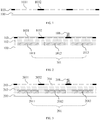
- the embodiment of the present invention provides a display substrate, which comprises a base substrate 100 and a polarization layer 103, wherein the polarization layer 103 includes GPs 1031 and light-shielding matrixes 1032 which are arranged in a same layer and integrally formed.
- the GPs and the light-shielding matrixes are integrated in the same layer, not only the production process is simplified but also the thickness of the LCD device is reduced.
- the embodiment of the present invention provides a display substrate, which comprises a base substrate 100, a quantum dot layer 101, a polarization layer 103, a planarization layer 102 disposed between the quantum dot layer 101 and the polarization layer 103, and spacers 108 disposed on one side of the polarization layer 103 away from the substrate 100, wherein the polarization layer 103 includes GPs 1031 and light-shielding matrixes 1032 which are arranged in a same layer and integrally formed.
- the GPs 1031 and the light-shielding matrixes 1032 in the polarization layer 103 may be made from a same material.
- the GPs 1031 and the light-shielding matrixes 1032 in the polarization layer 103 may be made from a same metallic material.
- the metallic material may be a metallic material commonly used in the field, e.g., Al, Cu, Au, Ag, Cr or an alloy of the metals.
- the planarization layer 103 may be made from resins containing an amount of polar bonds.
- the polar bonds include hydroxyl, carboxyl, carbonyl, ether bond, isocyanate group and urethano.
- the resin materials containing more polar bonds include epoxy resins, phenolic resins, urea resins, acrylic resins, polyvinyl alcohol, polyurethane, rubber, vinyl acetate and copolymers thereof, polystyrene and copolymers thereof, organo-silicon compounds and epoxy phenolic resins.
- urethane resin materials surfaces of metallic materials have large tension, belong to high-energy surfaces, and generally contain adsorbed water, hydroxyl group and other polar groups; the urethane resin materials may react with active sites such as adsorbed water and hydroxyl group to form covalent bonds; meanwhile, type-2 chemical bonds can also be formed by polar groups such as carbamate and sustituted urea in the urethane resin materials and polar groups on the surfaces of the metallic materials; and in addition, coordinate bonds can also be formed by the metallic materials and benzene rings in aromatic polyurethane. Due to the formation of the chemical bonds or the coordinate bonds, effective connection is formed between the polarization layer 103 and the planarization layer 102, so that the adhesion between the polarization layer 103 and the planarization layer 102 can be enhanced.
- a material of the quantum dot layer 101 may be selected from quantum dot materials commonly used in the field, for instance, may be one or more selected from the following materials: CdS, CdSe, CdTe, ZnO, ZnS, ZnSe, ZnTe, GaAs, GaP, GaSb, HgS, HgSe, HgTe, InAs, InP, InSb, AlAs, AlP, CuInS, CuInSe and AlSb.
- the emission spectrum of quantum dots may be controlled by the size of the quantum dots, namely the quantum dots may emit light of different colors in different sizes.
- the material of the quantum dots includes but not limited to the above enumerated several materials.
- the size of quantum dots for emitting red light generally ranges from 9 nm to 10 nm; the size of quantum dots for emitting yellow light is about 8 nm; and the size of quantum dots for emitting green light is about 7 nm.
- a pattern of the quantum dot layer 101 may be set according to actual demands.
- the quantum dot layer 101 may include patterned red quantum dot units 1011, patterned green quantum dot units 1012 and patterned blue quantum dot units 1013. Discrete red subpixels, green subpixels and blue subpixels are formed by the patterned red quantum dot units 1011, the patterned green quantum dot units 1012 and the patterned blue quantum dot units 1013.
- the quantum dot layer 101 may also include patterned quantum dot units of other colors, e.g., patterned yellow quantum dot units.
- the polarization layer 103 includes GPs 1031 and light-shielding matrixes 1032 which are arranged in the same layer and integrally formed, a polarizer that is arranged after backlight runs through liquid crystals and before exciting the quantum dots can be omitted, and the problem of depolarization when the display substrate is applied to the LCD can be solved. Therefore, the complex step of arranging the polarizer is omitted, so the production process is simplified. Moreover, no glass substrate is required to be arranged, and the cost is reduced.
- Another means of increasing the adhesion between the polarization layer and the planarization layer is to further arrange an adhesive layer between the polarization layer and the planarization layer.
- the display substrate comprises a base substrate 200, a quantum dot layer 201, a polarization layer 203, a planarization layer 202 disposed between the quantum dot layer 201 and the polarization layer 203, and spacers 208 disposed on one side of the polarization layer 203 away from the substrate 200, wherein the polarization layer 203 includes GPs 2031 and light-shielding matrixes 2032 which are arranged in a same layer and integrally formed.
- An adhesive layer 204 is further disposed between the polarization layer 203 and the planarization layer 202.
- the adhesive layer 204 is generally made from inorganic materials, e.g., ITO and IZO.
- the adhesive layer 204 made from the above materials may simultaneously provide enough adhesion for the polarization layer 203 made from metallic materials and the planarization layer 202 made from polymer materials, so the planarization layer 202 may not adopt specified resin materials and any materials of the planarization layer commonly used in the present field satisfy the requirement.
- the embodiment of the present invention further provides a method for manufacturing a display substrate.
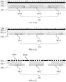
- a quantum dot layer 101 is formed on a substrate 100, and a planarization layer 102 is formed on the quantum dot layer 101.
- the quantum dot layer 101 may include discrete patterned quantum dot units of different colors.
- the quantum dot layer 101 is formed by 3 discrete patterned quantum dot units 1011, 1012 and 1013.
- the 3 patterned quantum dot units can emit different light under the excitation of backlight. For instance, the pattern unit 1011 emits red light; the pattern unit 1012 emits green light; and the pattern unit 1013 emits blue light. Thus, full color display can be achieved.
- the method for forming the quantum dot layer 101 and the planarization layer 102 may adopt the method commonly used in the present field, e.g., coating-exposure-development. No further description will be given here.
- a metal film 105 is deposited on the planarization layer 102.
- a material of the metal film 105 may be a metallic material commonly used in the field, e.g., Al, Cu, Au, Ag, Cr or an alloy of the above metals.
- a photoresist layer 106 is formed by coating photoresist on the metal film 105. Any conventional photoresist for etching metal in the present field may be used.
- the photoresist adopted in the present embodiment is polymethyl methacrylate (PMMA).
- the photoresist layer 106 is heated or subjected to UV-irradiation and softened, and a mask 107 is impressed into the photoresist layer 106 to form a structure corresponding to the GPs and the light-shielding matrixes.
- the manufacturing method of the mask 107 may include: forming a structure corresponding to the GPs and the light-shielding matrixes on the base substrate such as SiO 2 or Si substrate by electron-beam-direct-writing technology.
- the mask 107 is removed and the photoresist layer 106 on which the structure corresponding to the GPs and the light-shielding matrices is impressed is retained.
- the metal film is etched and cleaned, and the GPs 1031 are formed.
- the metal film 105 becomes the polarization layer 103 including the GPs 1031 and the light-shielding matrixes 1032 which are integrated.
- the GPs 1031 and the light-shielding matrixes 1032 are integrated on the polarization layer 103 by nano-printing technology, so one patterning process of the light-shielding matrixes is reduced, and hence the production process is simplified and the cost is reduced.
- the polarization layer 103 on which the GPs 1031 and the light-shielding matrixes 1032 are integrated can solve the problem of depolarization of quantum dots, and a polarizer that is arranged after backlight runs through liquid crystals and before exciting the quantum dots can be omitted, so that the structure of luminescent devices can be simplified and the cost can be further reduced.
- the method for manufacturing a display substrate in which an adhesive layer is further disposed between the polarization layer and the planarization layer is basically the same with the above method, except that after forming the planarization layer and before depositing the metal film, the method further comprising forming the adhesive layer on the planarization layer.
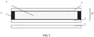
- the LCD device 10 comprises an array substrate 2 and an automatic opposing substrate 3 arranged opposite to the array substrate 2.
- the array substrate 2 and the opposing substrate 3 are arranged opposite to each other to form a liquid crystal cell and sealed by a sealant 6, and liquid crystal 4 are filled in the liquid crystal cell.
- the opposing substrate 3 is a CF substrate as described above.
- the array substrate 2 includes an array of pixel units. A pixel electrode of each pixel unit is configured to apply an electric field to control the rotation degree of liquid crystal, so as to achieve display.
- the LCD device 10 further comprises a backlight 5 which is configured to provide backlight for the array substrate. Light emitted by the backlight 5 enters the liquid crystal cell from one side of the array substrate 2 and emits out from one side of the opposing substrate (CF substrate) 3.
- the LCD device may be any product or component with display function such as an LCD panel, e-paper, a mobile phone, a tablet PC, a TV, a display, a notebook computer, a digital picture frame and a navigator.
Landscapes
- Physics & Mathematics (AREA)
- Nonlinear Science (AREA)
- General Physics & Mathematics (AREA)
- Optics & Photonics (AREA)
- Chemical & Material Sciences (AREA)
- Mathematical Physics (AREA)
- Crystallography & Structural Chemistry (AREA)
- Engineering & Computer Science (AREA)
- Microelectronics & Electronic Packaging (AREA)
- Chemical Kinetics & Catalysis (AREA)
- General Chemical & Material Sciences (AREA)
- Manufacturing & Machinery (AREA)
- Polarising Elements (AREA)
- Devices For Indicating Variable Information By Combining Individual Elements (AREA)
- Liquid Crystal (AREA)
Applications Claiming Priority (2)
| Application Number | Priority Date | Filing Date | Title |
|---|---|---|---|
| CN201510527566.4A CN105182594B (zh) | 2015-08-25 | 2015-08-25 | 显示基板 |
| PCT/CN2016/072826 WO2017031951A1 (zh) | 2015-08-25 | 2016-01-29 | 显示基板 |
Publications (2)
| Publication Number | Publication Date |
|---|---|
| EP3343280A1 true EP3343280A1 (de) | 2018-07-04 |
| EP3343280A4 EP3343280A4 (de) | 2019-03-06 |
Family
ID=54904769
Family Applications (1)
| Application Number | Title | Priority Date | Filing Date |
|---|---|---|---|
| EP16760636.7A Withdrawn EP3343280A4 (de) | 2015-08-25 | 2016-01-29 | Anzeigesubstrat |
Country Status (4)
| Country | Link |
|---|---|
| US (1) | US10209557B2 (de) |
| EP (1) | EP3343280A4 (de) |
| CN (1) | CN105182594B (de) |
| WO (1) | WO2017031951A1 (de) |
Families Citing this family (25)
| Publication number | Priority date | Publication date | Assignee | Title |
|---|---|---|---|---|
| CN105182594B (zh) | 2015-08-25 | 2018-07-31 | 京东方科技集团股份有限公司 | 显示基板 |
| KR20170136109A (ko) * | 2016-05-31 | 2017-12-11 | 삼성디스플레이 주식회사 | 색변환 패널 및 이를 포함하는 표시 장치 |
| CN105911628B (zh) * | 2016-06-07 | 2018-08-07 | 京东方科技集团股份有限公司 | 一种线栅偏振器结构、显示基板母板及制作方法 |
| CN106597762A (zh) * | 2016-10-28 | 2017-04-26 | 深圳市华星光电技术有限公司 | 线栅偏光电极及其压印模具和制作方法、显示基板 |
| CN108241187B (zh) * | 2016-12-23 | 2024-03-15 | 苏州星烁纳米科技有限公司 | 量子点偏光片、液晶面板及液晶显示装置 |
| KR102707517B1 (ko) * | 2017-01-19 | 2024-09-23 | 삼성디스플레이 주식회사 | 표시 장치 및 이의 제조 방법 |
| CN106855648A (zh) * | 2017-02-04 | 2017-06-16 | 苏州星烁纳米科技有限公司 | 量子点偏光元件、背光模组及液晶显示装置 |
| CN106773228B (zh) * | 2017-03-09 | 2020-01-03 | 深圳市华星光电技术有限公司 | 显示面板的制造方法、线栅偏光片及其制造方法 |
| US10509257B2 (en) | 2017-03-29 | 2019-12-17 | Shenzhen China Star Optoelectronics Technology Co., Ltd | Display panels, wire grid polarizers, and the manufacturing methods thereof |
| CN106842404A (zh) * | 2017-03-29 | 2017-06-13 | 深圳市华星光电技术有限公司 | 显示面板、线栅偏光片及其制造方法 |
| CN107141484B (zh) * | 2017-05-11 | 2020-12-22 | 京东方科技集团股份有限公司 | 一种有机树脂及其制备方法、显示基板及其制备方法 |
| US10302990B2 (en) | 2017-07-26 | 2019-05-28 | A.U. Vista, Inc. | Display cell structure and display device using quantum dot |
| CN109422987B (zh) | 2017-08-30 | 2021-03-09 | 京东方科技集团股份有限公司 | 平坦层用组合物、其制备方法、平坦层材料及显示装置 |
| CN107807470A (zh) * | 2017-10-19 | 2018-03-16 | 深圳市华星光电技术有限公司 | 金属栅偏光片及显示面板 |
| CN108169950A (zh) * | 2017-12-26 | 2018-06-15 | 深圳市华星光电技术有限公司 | 彩膜基板及其制作方法、液晶面板 |
| CN108415192A (zh) * | 2018-03-26 | 2018-08-17 | 京东方科技集团股份有限公司 | 一种显示基板、显示面板、显示装置及其制作方法 |
| CN108508521A (zh) * | 2018-03-30 | 2018-09-07 | 武汉华星光电技术有限公司 | 具有遮光层的偏振光栅及其制作方法、阵列基板、显示面板、显示模组及终端 |
| CN108363135B (zh) * | 2018-04-19 | 2020-08-07 | 京东方科技集团股份有限公司 | 柔性偏光片及制作方法、显示装置 |
| CN109445247B (zh) * | 2018-11-16 | 2020-06-19 | 京东方科技集团股份有限公司 | 压印模板及其制备方法和压印方法 |
| CN110137184B (zh) | 2019-05-27 | 2021-09-21 | 京东方科技集团股份有限公司 | 一种阵列基板、显示面板和显示装置 |
| WO2021174392A1 (zh) * | 2020-03-02 | 2021-09-10 | 京东方科技集团股份有限公司 | 偏光片、电子装置及制备偏光片的方法 |
| CN111338124A (zh) * | 2020-04-13 | 2020-06-26 | 武汉华星光电技术有限公司 | 一种量子点显示面板、量子点显示装置及其制备方法 |
| CN113093430B (zh) * | 2021-04-01 | 2023-12-12 | 京东方科技集团股份有限公司 | 显示面板及其制备方法、显示装置 |
| KR20230063687A (ko) * | 2021-11-02 | 2023-05-09 | 삼성전자주식회사 | 양자점 박막 및 그 제조 방법, 이를 포함하는 광전 소자 및 이미지 센서 |
| CN114994821B (zh) * | 2022-06-16 | 2024-09-17 | 昆山国显光电有限公司 | 偏光片以及显示模组 |
Family Cites Families (22)
| Publication number | Priority date | Publication date | Assignee | Title |
|---|---|---|---|---|
| JP3165100B2 (ja) * | 1998-02-09 | 2001-05-14 | 日本電気株式会社 | 液晶表示装置とその製造方法 |
| JP4695101B2 (ja) * | 2007-01-24 | 2011-06-08 | 株式会社 日立ディスプレイズ | 偏光子及びそれを用いた液晶表示装置 |
| JP2009042319A (ja) * | 2007-08-07 | 2009-02-26 | Sony Corp | 液晶表示装置及び液晶表示装置の製造方法 |
| US8294848B2 (en) * | 2008-10-01 | 2012-10-23 | Samsung Display Co., Ltd. | Liquid crystal display having light diffusion layer |
| US20120057106A1 (en) * | 2010-09-07 | 2012-03-08 | Electronics And Telecommunications Research Institute | Polarizer and liquid crystal display |
| CN102650823A (zh) * | 2011-05-13 | 2012-08-29 | 京东方科技集团股份有限公司 | 具有偏振能力的彩色滤光片及其制作方法 |
| CN103596740A (zh) * | 2011-06-10 | 2014-02-19 | 富士胶片株式会社 | 可剥离性层合膜、可剥离性层合膜卷、其制备方法、膜、光学膜、偏振板、偏振板的制备方法以及液晶显示装置 |
| KR101841619B1 (ko) * | 2011-11-14 | 2018-03-26 | 삼성디스플레이 주식회사 | 금속선 격자 편광소자를 포함하는 액정 표시 장치 및 그 제조 방법 |
| US9057880B2 (en) * | 2011-11-30 | 2015-06-16 | Reald Inc. | Laser beam scanned display apparatus and method thereof |
| KR101942363B1 (ko) * | 2012-07-26 | 2019-04-12 | 삼성디스플레이 주식회사 | 편광 소자, 이의 제조 방법, 이를 포함하는 표시 패널 및 이를 포함하는 표시 장치 |
| KR101961427B1 (ko) * | 2012-10-29 | 2019-03-25 | 삼성디스플레이 주식회사 | 액정 표시 장치 및 이를 제조하는 방법 |
| CN102944943B (zh) | 2012-11-09 | 2016-03-16 | 京东方科技集团股份有限公司 | 量子点彩色滤光片、液晶面板及显示装置 |
| CN103412436B (zh) * | 2013-07-24 | 2015-09-30 | 北京京东方光电科技有限公司 | 一种彩膜基板、液晶显示屏及单色量子点的分散方法 |
| JP2015051084A (ja) * | 2013-09-06 | 2015-03-19 | 淑子 山敷 | 洗濯補助具 |
| JP6404036B2 (ja) * | 2014-03-05 | 2018-10-10 | 富士フイルム株式会社 | 偏光板の製造方法 |
| KR20160137632A (ko) * | 2014-03-26 | 2016-11-30 | 메르크 파텐트 게엠베하 | 편광 방사 디바이스 |
| KR20160056460A (ko) * | 2014-11-11 | 2016-05-20 | 삼성디스플레이 주식회사 | 곡면 표시 장치 |
| CN104330918A (zh) * | 2014-11-28 | 2015-02-04 | 京东方科技集团股份有限公司 | 一种显示面板和显示装置 |
| WO2016093280A1 (ja) * | 2014-12-10 | 2016-06-16 | 積水化学工業株式会社 | 透明接着剤付き偏光板、及び、タッチパネル |
| CN104516164B (zh) * | 2015-01-05 | 2018-03-09 | 京东方科技集团股份有限公司 | 一种显示基板及其制作方法和显示装置 |
| CN104808383A (zh) * | 2015-05-15 | 2015-07-29 | 京东方科技集团股份有限公司 | 一种显示基板、其制作方法、显示面板及显示装置 |
| CN105182594B (zh) | 2015-08-25 | 2018-07-31 | 京东方科技集团股份有限公司 | 显示基板 |
-
2015
- 2015-08-25 CN CN201510527566.4A patent/CN105182594B/zh active Active
-
2016
- 2016-01-29 EP EP16760636.7A patent/EP3343280A4/de not_active Withdrawn
- 2016-01-29 US US15/126,020 patent/US10209557B2/en active Active
- 2016-01-29 WO PCT/CN2016/072826 patent/WO2017031951A1/zh not_active Ceased
Also Published As
| Publication number | Publication date |
|---|---|
| EP3343280A4 (de) | 2019-03-06 |
| US10209557B2 (en) | 2019-02-19 |
| WO2017031951A1 (zh) | 2017-03-02 |
| CN105182594A (zh) | 2015-12-23 |
| CN105182594B (zh) | 2018-07-31 |
| US20170261806A1 (en) | 2017-09-14 |
Similar Documents
| Publication | Publication Date | Title |
|---|---|---|
| US10209557B2 (en) | Display substrate | |
| US9823510B2 (en) | Quantum dot color film substrate, manufacturing method thereof and LCD apparatus | |
| EP2680069B1 (de) | Quantenstab-LED-Anzeigevorrichtung | |
| US9804489B2 (en) | Method for manufacturing quantum dot color filter | |
| US10534232B2 (en) | Array substrate and manufacturing method thereof | |
| US20210088840A1 (en) | Method of having a polarizer built in a lcd panel, lcd device, and lcd device manufacturing method | |
| US20170269274A1 (en) | Method for manufacturing quantum dot polarization plate | |
| US20260026229A1 (en) | Display panel and color filter substrate | |
| KR102931285B1 (ko) | 표시 장치 및 그 제조 방법 | |
| US9636900B2 (en) | Display substrate and method for manufacturing the same, and display device | |
| EP2919267B1 (de) | Arraysubstrat, herstellungsverfahren dafür und anzeigevorrichtung | |
| CN206039109U (zh) | 显示层结构及显示模块 | |
| JP7456435B2 (ja) | 量子ドット色変換層における色域性能及び効率の増大 | |
| CN105182610A (zh) | 一种显示基板及其制作方法、显示装置 | |
| CN105700222B (zh) | 量子点彩膜基板及其制作方法、显示装置 | |
| KR101353566B1 (ko) | 전기영동 표시장치의 제조방법 | |
| KR102200347B1 (ko) | 퀀텀 로드 표시장치 및 그 제조 방법 | |
| US10338429B2 (en) | Method for manufacturing quantum dot color filter | |
| CN105137648A (zh) | Coa基板及其制备方法、显示装置 | |
| CN105183229B (zh) | 显示面板、触控显示面板及其制作方法、显示装置 | |
| KR101748699B1 (ko) | 전기영동 표시소자 및 그 제조방법 | |
| CN108445672A (zh) | 量子点液晶显示面板及制作方法 | |
| KR102112755B1 (ko) | 표시 장치 및 그 제조 방법 | |
| US12433130B2 (en) | Color converting substrate and display device comprising same | |
| KR101748702B1 (ko) | 격벽조성물, 이를 구비한 전기영동 표시소자 및 그 제조방법 |
Legal Events
| Date | Code | Title | Description |
|---|---|---|---|
| STAA | Information on the status of an ep patent application or granted ep patent |
Free format text: STATUS: THE INTERNATIONAL PUBLICATION HAS BEEN MADE |
|
| PUAI | Public reference made under article 153(3) epc to a published international application that has entered the european phase |
Free format text: ORIGINAL CODE: 0009012 |
|
| STAA | Information on the status of an ep patent application or granted ep patent |
Free format text: STATUS: REQUEST FOR EXAMINATION WAS MADE |
|
| 17P | Request for examination filed |
Effective date: 20160915 |
|
| AK | Designated contracting states |
Kind code of ref document: A1 Designated state(s): AL AT BE BG CH CY CZ DE DK EE ES FI FR GB GR HR HU IE IS IT LI LT LU LV MC MK MT NL NO PL PT RO RS SE SI SK SM TR |
|
| AX | Request for extension of the european patent |
Extension state: BA ME |
|
| DAV | Request for validation of the european patent (deleted) | ||
| DAX | Request for extension of the european patent (deleted) | ||
| A4 | Supplementary search report drawn up and despatched |
Effective date: 20190205 |
|
| RIC1 | Information provided on ipc code assigned before grant |
Ipc: G02F 1/1333 20060101ALN20190130BHEP Ipc: G03F 7/00 20060101ALN20190130BHEP Ipc: G02F 1/1335 20060101ALI20190130BHEP Ipc: G02F 1/1362 20060101ALN20190130BHEP Ipc: G02B 5/30 20060101ALN20190130BHEP Ipc: G02F 1/13357 20060101AFI20190130BHEP |
|
| STAA | Information on the status of an ep patent application or granted ep patent |
Free format text: STATUS: EXAMINATION IS IN PROGRESS |
|
| 17Q | First examination report despatched |
Effective date: 20210331 |
|
| STAA | Information on the status of an ep patent application or granted ep patent |
Free format text: STATUS: THE APPLICATION IS DEEMED TO BE WITHDRAWN |
|
| 18D | Application deemed to be withdrawn |
Effective date: 20220802 |