EP3343557A2 - Organische lichtemittierende anzeigevorrichtung und ansteuerungsverfahren dafür - Google Patents
Organische lichtemittierende anzeigevorrichtung und ansteuerungsverfahren dafür Download PDFInfo
- Publication number
- EP3343557A2 EP3343557A2 EP17207918.8A EP17207918A EP3343557A2 EP 3343557 A2 EP3343557 A2 EP 3343557A2 EP 17207918 A EP17207918 A EP 17207918A EP 3343557 A2 EP3343557 A2 EP 3343557A2
- Authority
- EP
- European Patent Office
- Prior art keywords
- gate
- pixel
- signal
- line
- emission control
- Prior art date
- Legal status (The legal status is an assumption and is not a legal conclusion. Google has not performed a legal analysis and makes no representation as to the accuracy of the status listed.)
- Granted
Links
Images


Classifications
-
- G—PHYSICS
- G09—EDUCATION; CRYPTOGRAPHY; DISPLAY; ADVERTISING; SEALS
- G09G—ARRANGEMENTS OR CIRCUITS FOR CONTROL OF INDICATING DEVICES USING STATIC MEANS TO PRESENT VARIABLE INFORMATION
- G09G3/00—Control arrangements or circuits, of interest only in connection with visual indicators other than cathode-ray tubes
- G09G3/20—Control arrangements or circuits, of interest only in connection with visual indicators other than cathode-ray tubes for presentation of an assembly of a number of characters, e.g. a page, by composing the assembly by combination of individual elements arranged in a matrix no fixed position being assigned to or needed to be assigned to the individual characters or partial characters
- G09G3/22—Control arrangements or circuits, of interest only in connection with visual indicators other than cathode-ray tubes for presentation of an assembly of a number of characters, e.g. a page, by composing the assembly by combination of individual elements arranged in a matrix no fixed position being assigned to or needed to be assigned to the individual characters or partial characters using controlled light sources
- G09G3/30—Control arrangements or circuits, of interest only in connection with visual indicators other than cathode-ray tubes for presentation of an assembly of a number of characters, e.g. a page, by composing the assembly by combination of individual elements arranged in a matrix no fixed position being assigned to or needed to be assigned to the individual characters or partial characters using controlled light sources using electroluminescent panels
- G09G3/32—Control arrangements or circuits, of interest only in connection with visual indicators other than cathode-ray tubes for presentation of an assembly of a number of characters, e.g. a page, by composing the assembly by combination of individual elements arranged in a matrix no fixed position being assigned to or needed to be assigned to the individual characters or partial characters using controlled light sources using electroluminescent panels semiconductive, e.g. using light-emitting diodes [LED]
- G09G3/3208—Control arrangements or circuits, of interest only in connection with visual indicators other than cathode-ray tubes for presentation of an assembly of a number of characters, e.g. a page, by composing the assembly by combination of individual elements arranged in a matrix no fixed position being assigned to or needed to be assigned to the individual characters or partial characters using controlled light sources using electroluminescent panels semiconductive, e.g. using light-emitting diodes [LED] organic, e.g. using organic light-emitting diodes [OLED]
- G09G3/3225—Control arrangements or circuits, of interest only in connection with visual indicators other than cathode-ray tubes for presentation of an assembly of a number of characters, e.g. a page, by composing the assembly by combination of individual elements arranged in a matrix no fixed position being assigned to or needed to be assigned to the individual characters or partial characters using controlled light sources using electroluminescent panels semiconductive, e.g. using light-emitting diodes [LED] organic, e.g. using organic light-emitting diodes [OLED] using an active matrix
-
- G—PHYSICS
- G09—EDUCATION; CRYPTOGRAPHY; DISPLAY; ADVERTISING; SEALS
- G09G—ARRANGEMENTS OR CIRCUITS FOR CONTROL OF INDICATING DEVICES USING STATIC MEANS TO PRESENT VARIABLE INFORMATION
- G09G3/00—Control arrangements or circuits, of interest only in connection with visual indicators other than cathode-ray tubes
- G09G3/20—Control arrangements or circuits, of interest only in connection with visual indicators other than cathode-ray tubes for presentation of an assembly of a number of characters, e.g. a page, by composing the assembly by combination of individual elements arranged in a matrix no fixed position being assigned to or needed to be assigned to the individual characters or partial characters
- G09G3/22—Control arrangements or circuits, of interest only in connection with visual indicators other than cathode-ray tubes for presentation of an assembly of a number of characters, e.g. a page, by composing the assembly by combination of individual elements arranged in a matrix no fixed position being assigned to or needed to be assigned to the individual characters or partial characters using controlled light sources
- G09G3/30—Control arrangements or circuits, of interest only in connection with visual indicators other than cathode-ray tubes for presentation of an assembly of a number of characters, e.g. a page, by composing the assembly by combination of individual elements arranged in a matrix no fixed position being assigned to or needed to be assigned to the individual characters or partial characters using controlled light sources using electroluminescent panels
- G09G3/32—Control arrangements or circuits, of interest only in connection with visual indicators other than cathode-ray tubes for presentation of an assembly of a number of characters, e.g. a page, by composing the assembly by combination of individual elements arranged in a matrix no fixed position being assigned to or needed to be assigned to the individual characters or partial characters using controlled light sources using electroluminescent panels semiconductive, e.g. using light-emitting diodes [LED]
- G09G3/3208—Control arrangements or circuits, of interest only in connection with visual indicators other than cathode-ray tubes for presentation of an assembly of a number of characters, e.g. a page, by composing the assembly by combination of individual elements arranged in a matrix no fixed position being assigned to or needed to be assigned to the individual characters or partial characters using controlled light sources using electroluminescent panels semiconductive, e.g. using light-emitting diodes [LED] organic, e.g. using organic light-emitting diodes [OLED]
- G09G3/3225—Control arrangements or circuits, of interest only in connection with visual indicators other than cathode-ray tubes for presentation of an assembly of a number of characters, e.g. a page, by composing the assembly by combination of individual elements arranged in a matrix no fixed position being assigned to or needed to be assigned to the individual characters or partial characters using controlled light sources using electroluminescent panels semiconductive, e.g. using light-emitting diodes [LED] organic, e.g. using organic light-emitting diodes [OLED] using an active matrix
- G09G3/3233—Control arrangements or circuits, of interest only in connection with visual indicators other than cathode-ray tubes for presentation of an assembly of a number of characters, e.g. a page, by composing the assembly by combination of individual elements arranged in a matrix no fixed position being assigned to or needed to be assigned to the individual characters or partial characters using controlled light sources using electroluminescent panels semiconductive, e.g. using light-emitting diodes [LED] organic, e.g. using organic light-emitting diodes [OLED] using an active matrix with pixel circuitry controlling the current through the light-emitting element
-
- G—PHYSICS
- G09—EDUCATION; CRYPTOGRAPHY; DISPLAY; ADVERTISING; SEALS
- G09G—ARRANGEMENTS OR CIRCUITS FOR CONTROL OF INDICATING DEVICES USING STATIC MEANS TO PRESENT VARIABLE INFORMATION
- G09G3/00—Control arrangements or circuits, of interest only in connection with visual indicators other than cathode-ray tubes
- G09G3/20—Control arrangements or circuits, of interest only in connection with visual indicators other than cathode-ray tubes for presentation of an assembly of a number of characters, e.g. a page, by composing the assembly by combination of individual elements arranged in a matrix no fixed position being assigned to or needed to be assigned to the individual characters or partial characters
- G09G3/22—Control arrangements or circuits, of interest only in connection with visual indicators other than cathode-ray tubes for presentation of an assembly of a number of characters, e.g. a page, by composing the assembly by combination of individual elements arranged in a matrix no fixed position being assigned to or needed to be assigned to the individual characters or partial characters using controlled light sources
- G09G3/30—Control arrangements or circuits, of interest only in connection with visual indicators other than cathode-ray tubes for presentation of an assembly of a number of characters, e.g. a page, by composing the assembly by combination of individual elements arranged in a matrix no fixed position being assigned to or needed to be assigned to the individual characters or partial characters using controlled light sources using electroluminescent panels
- G09G3/32—Control arrangements or circuits, of interest only in connection with visual indicators other than cathode-ray tubes for presentation of an assembly of a number of characters, e.g. a page, by composing the assembly by combination of individual elements arranged in a matrix no fixed position being assigned to or needed to be assigned to the individual characters or partial characters using controlled light sources using electroluminescent panels semiconductive, e.g. using light-emitting diodes [LED]
- G09G3/3208—Control arrangements or circuits, of interest only in connection with visual indicators other than cathode-ray tubes for presentation of an assembly of a number of characters, e.g. a page, by composing the assembly by combination of individual elements arranged in a matrix no fixed position being assigned to or needed to be assigned to the individual characters or partial characters using controlled light sources using electroluminescent panels semiconductive, e.g. using light-emitting diodes [LED] organic, e.g. using organic light-emitting diodes [OLED]
- G09G3/3225—Control arrangements or circuits, of interest only in connection with visual indicators other than cathode-ray tubes for presentation of an assembly of a number of characters, e.g. a page, by composing the assembly by combination of individual elements arranged in a matrix no fixed position being assigned to or needed to be assigned to the individual characters or partial characters using controlled light sources using electroluminescent panels semiconductive, e.g. using light-emitting diodes [LED] organic, e.g. using organic light-emitting diodes [OLED] using an active matrix
- G09G3/3258—Control arrangements or circuits, of interest only in connection with visual indicators other than cathode-ray tubes for presentation of an assembly of a number of characters, e.g. a page, by composing the assembly by combination of individual elements arranged in a matrix no fixed position being assigned to or needed to be assigned to the individual characters or partial characters using controlled light sources using electroluminescent panels semiconductive, e.g. using light-emitting diodes [LED] organic, e.g. using organic light-emitting diodes [OLED] using an active matrix with pixel circuitry controlling the voltage across the light-emitting element
-
- H—ELECTRICITY
- H10—SEMICONDUCTOR DEVICES; ELECTRIC SOLID-STATE DEVICES NOT OTHERWISE PROVIDED FOR
- H10K—ORGANIC ELECTRIC SOLID-STATE DEVICES
- H10K59/00—Integrated devices, or assemblies of multiple devices, comprising at least one organic light-emitting element covered by group H10K50/00
- H10K59/10—OLED displays
- H10K59/12—Active-matrix OLED [AMOLED] displays
- H10K59/131—Interconnections, e.g. wiring lines or terminals
-
- G—PHYSICS
- G09—EDUCATION; CRYPTOGRAPHY; DISPLAY; ADVERTISING; SEALS
- G09G—ARRANGEMENTS OR CIRCUITS FOR CONTROL OF INDICATING DEVICES USING STATIC MEANS TO PRESENT VARIABLE INFORMATION
- G09G2300/00—Aspects of the constitution of display devices
- G09G2300/04—Structural and physical details of display devices
- G09G2300/0439—Pixel structures
- G09G2300/0465—Improved aperture ratio, e.g. by size reduction of the pixel circuit, e.g. for improving the pixel density or the maximum displayable luminance or brightness
-
- G—PHYSICS
- G09—EDUCATION; CRYPTOGRAPHY; DISPLAY; ADVERTISING; SEALS
- G09G—ARRANGEMENTS OR CIRCUITS FOR CONTROL OF INDICATING DEVICES USING STATIC MEANS TO PRESENT VARIABLE INFORMATION
- G09G2300/00—Aspects of the constitution of display devices
- G09G2300/08—Active matrix structure, i.e. with use of active elements, inclusive of non-linear two terminal elements, in the pixels together with light emitting or modulating elements
- G09G2300/0809—Several active elements per pixel in active matrix panels
- G09G2300/0819—Several active elements per pixel in active matrix panels used for counteracting undesired variations, e.g. feedback or autozeroing
-
- G—PHYSICS
- G09—EDUCATION; CRYPTOGRAPHY; DISPLAY; ADVERTISING; SEALS
- G09G—ARRANGEMENTS OR CIRCUITS FOR CONTROL OF INDICATING DEVICES USING STATIC MEANS TO PRESENT VARIABLE INFORMATION
- G09G2300/00—Aspects of the constitution of display devices
- G09G2300/08—Active matrix structure, i.e. with use of active elements, inclusive of non-linear two terminal elements, in the pixels together with light emitting or modulating elements
- G09G2300/0809—Several active elements per pixel in active matrix panels
- G09G2300/0842—Several active elements per pixel in active matrix panels forming a memory circuit, e.g. a dynamic memory with one capacitor
-
- G—PHYSICS
- G09—EDUCATION; CRYPTOGRAPHY; DISPLAY; ADVERTISING; SEALS
- G09G—ARRANGEMENTS OR CIRCUITS FOR CONTROL OF INDICATING DEVICES USING STATIC MEANS TO PRESENT VARIABLE INFORMATION
- G09G2300/00—Aspects of the constitution of display devices
- G09G2300/08—Active matrix structure, i.e. with use of active elements, inclusive of non-linear two terminal elements, in the pixels together with light emitting or modulating elements
- G09G2300/0809—Several active elements per pixel in active matrix panels
- G09G2300/0842—Several active elements per pixel in active matrix panels forming a memory circuit, e.g. a dynamic memory with one capacitor
- G09G2300/0861—Several active elements per pixel in active matrix panels forming a memory circuit, e.g. a dynamic memory with one capacitor with additional control of the display period without amending the charge stored in a pixel memory, e.g. by means of additional select electrodes
-
- G—PHYSICS
- G09—EDUCATION; CRYPTOGRAPHY; DISPLAY; ADVERTISING; SEALS
- G09G—ARRANGEMENTS OR CIRCUITS FOR CONTROL OF INDICATING DEVICES USING STATIC MEANS TO PRESENT VARIABLE INFORMATION
- G09G2310/00—Command of the display device
- G09G2310/02—Addressing, scanning or driving the display screen or processing steps related thereto
- G09G2310/0262—The addressing of the pixel, in a display other than an active matrix LCD, involving the control of two or more scan electrodes or two or more data electrodes, e.g. pixel voltage dependent on signals of two data electrodes
-
- G—PHYSICS
- G09—EDUCATION; CRYPTOGRAPHY; DISPLAY; ADVERTISING; SEALS
- G09G—ARRANGEMENTS OR CIRCUITS FOR CONTROL OF INDICATING DEVICES USING STATIC MEANS TO PRESENT VARIABLE INFORMATION
- G09G2310/00—Command of the display device
- G09G2310/02—Addressing, scanning or driving the display screen or processing steps related thereto
- G09G2310/0264—Details of driving circuits
-
- G—PHYSICS
- G09—EDUCATION; CRYPTOGRAPHY; DISPLAY; ADVERTISING; SEALS
- G09G—ARRANGEMENTS OR CIRCUITS FOR CONTROL OF INDICATING DEVICES USING STATIC MEANS TO PRESENT VARIABLE INFORMATION
- G09G2310/00—Command of the display device
- G09G2310/06—Details of flat display driving waveforms
- G09G2310/067—Special waveforms for scanning, where no circuit details of the gate driver are given
-
- G—PHYSICS
- G09—EDUCATION; CRYPTOGRAPHY; DISPLAY; ADVERTISING; SEALS
- G09G—ARRANGEMENTS OR CIRCUITS FOR CONTROL OF INDICATING DEVICES USING STATIC MEANS TO PRESENT VARIABLE INFORMATION
- G09G2320/00—Control of display operating conditions
- G09G2320/02—Improving the quality of display appearance
- G09G2320/0233—Improving the luminance or brightness uniformity across the screen
-
- G—PHYSICS
- G09—EDUCATION; CRYPTOGRAPHY; DISPLAY; ADVERTISING; SEALS
- G09G—ARRANGEMENTS OR CIRCUITS FOR CONTROL OF INDICATING DEVICES USING STATIC MEANS TO PRESENT VARIABLE INFORMATION
- G09G2320/00—Control of display operating conditions
- G09G2320/04—Maintaining the quality of display appearance
- G09G2320/043—Preventing or counteracting the effects of ageing
- G09G2320/045—Compensation of drifts in the characteristics of light emitting or modulating elements
Definitions
- the present disclosure relates to an organic light-emitting display device and a driving method thereof.
- OLEDs organic light-emitting diodes
- Respective OLEDs have an organic compound layer situated between an anode and a cathode.
- the organic compound layer includes a hole injection layer (HIL), a hole transport layer (HTL), an emission layer (EML), an electron transport layer (ETL), and an electron injection layer (EIL).
- HIL hole injection layer
- HTL hole transport layer
- EML emission layer
- ETL electron transport layer
- EIL electron injection layer
- the luminance of organic light-emitting display devices may be non-uniform due to, for example, a deviation in threshold voltages of driving transistors applying driving currents to OLEDs and the threshold voltages of OLEDs.
- organic light-emitting display devices utilize an initialization voltage and an emission control signal, in addition to a data signal and a gate signal.
- organic light-emitting display devices require a time period in which gate voltages of driving transistors of pixels connected to gate lines corresponding thereto are initialized and the threshold voltages of the driving transistors and threshold voltages of the organic light-emitting diodes are sensed or compensated for. This may consequently complexify a driving block including OLEDs, as well as driving timing. When the driving block and driving timing of a display device become complexi-fied, it may be difficult to use the display device in a high resolution application.
- Various aspects of the present disclosure provide an organic light-emitting display device, able to reduce the size of a non-display area, and a driving method thereof.
- an organic light-emitting display device capable of compensating for a threshold voltage and simplifying driving timing to be used in high resolution applications, and a driving method thereof
- an organic light-emitting display device may include: a display panel including a plurality of gate lines, a plurality of data lines intersecting the plurality of gate lines, a plurality of pixels emitting light by receiving gate signals and data signals through the plurality of gate lines and the plurality of data lines; a data driver delivering the data signals to the display panel; and a gate driver delivering the gate signals and an emission control signal.
- a first pixel of the plurality of pixels may be initialized in response to a first gate signal of the gate signals, may receive a first data signal input thereto in response to a second gate signal generated after the first gate signal, and may be controlled by the emission control signal to emit light in response to the first data signal.
- a second pixel of the plurality of pixels may be initialized in response to the second gate signal, may receive a second data signal input thereto in response to a third gate signal generated after the second gate signal, and may be controlled by the emission control signal to emit light in response to the second data signal.
- a pixel circuit may include: a first transistor having a first electrode connected to a reference voltage line, a second electrode connected to a third node, and a gate electrode connected to a first gate line; a second transistor having a first electrode connected to a data line, a second electrode connected to a first node, and a gate electrode connected to a second gate line; a third transistor having a first electrode connected to a second node, a second electrode connected to the third node, and a gate electrode connected to the second gate line; a fourth transistor having a first electrode connected to the reference line, a second electrode connected to the first node, and a gate electrode connected to an emission control line; a fifth transistor having a first electrode connected to the second node, a second electrode connected to an anode of an organic light-emitting diode (OLED), and a gate electrode connected to the emission control line; a sixth transistor having a first electrode connected to the reference voltage line, a second electrode connected to the an OLED
- a method of driving an organic light-emitting display device may include: sequentially initializing two pixels connected to a single date line; sequentially sampling threshold voltages of the two pixels and inputting a data signal to the two pixels; and simultaneously emitting light from two pixels.
- an organic light-emitting display device comprising a display panel comprising a plurality of gate lines, a plurality of emission control lines, a plurality of data lines intersecting the plurality of gate lines, and a plurality of pixels including at least a first pixel and a second pixel, a data driver delivering data signals to the pixels, and a gate driver delivering gate signals and emission control signals to the pixels.
- the gate driver is electrically connected to at least a first gate line, a second gate line, and a third gate line of the gate lines, and an emission control line.
- the first pixel is electrically connected to the first gate line and the second gate line, the first pixel being initialized responsive to a first gate signal via the first gate line, a first data voltage being input to the first pixel responsive to a second gate signal via the second gate line, and the first pixel emitting light according to the first data voltage responsive to an emission control signal via the emission control line.
- the second pixel is electrically connected to the second gate line and the third gate line, the second pixel being initialized responsive to a second gate signal via the second gate line, a second data voltage being input to the second pixel responsive to a third gate signal via the third gate line, and the second pixel emitting light according to the second data voltage responsive to the same emission control signal via the emission control line. Both the first pixel and the second pixel may emit light simultaneously in response to the same emission control signal.
- the first pixel maintains the first gate signal without emitting light while the second data signal is being input to the second pixel.
- the gate driver comprises a first gate circuit connected to a first gate line of the plurality of gate lines, a second gate circuit connected to a second gate line thereof, a third gate circuit connected to a third gate line thereof, and an emission control circuit connected to said one of the emission control lines.
- the first pixel is initialized during a first time period
- the first data voltage is input to the first pixel and the second pixel is initialized during a second time period subsequent to the first time period
- the second data voltage is input to the second pixel during a third time period subsequent to the second time period
- both the first pixel and the second pixel emit light according to the first data voltage and the second data voltage, respectively, during a fourth time period subsequent to the third time period.
- the first data voltage is held in the first pixel during the third time period.
- a first threshold voltage of a first driving transistor in the first pixel is sensed during the second time period, and a second threshold voltage of a second driving transistor in the second pixel is sensed during the third time period.
- the number of the gate lines connected to the gate driver is triple the number of the emission control lines connected to the gate driver.
- Each of the emission control lines may be electrically connected to two corresponding ones of the pixels of the display panel.
- one emission control line is connected to two pixels or in different words, two pixels are only connected to one emission control line.
- the organic light-emitting display device and the driving method thereof can reduce the size of a non-display area.
- the organic light-emitting display device and the driving method thereof can compensate for a threshold voltage and simplify driving timing such that the organic light-emitting display device can be used in high resolution applications.
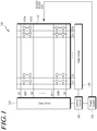
- FIG. 1 is a configuration view illustrating an organic light-emitting display device 100 according to exemplary embodiments.
- the organic light-emitting display device 100 includes a display panel 110, a gate driver 120, a data driver 130, a control circuit 140, and a power supply 150.
- the display panel 110 includes a plurality of pixels (or subpixels) 101.
- Each of the plurality of pixels 101 includes an organic light-emitting diode (OLED, not shown) and a pixel circuit (not shown) allowing a driving current to flow into the OLED.
- the pixel circuit of each of the plurality of pixels 101 may generate a driving current using a data signal delivered thereto in response to a gate signal, as well as a voltage supplied from a first power source, and may deliver the driving current to the OLED in response to an emission control signal.
- each of the plurality of pixels 101 may be initialized by a reference voltage Vref delivered thereto and may compensate for the threshold voltage of the OLED, as well as the threshold voltage of a driving transistor included in each of the plurality of pixels 101.
- the plurality of pixels 101 are arranged in pixel areas defined by a plurality of gate lines G1, G2, ..., Gn-1, and Gn, intersecting a plurality of data lines D1, D2, ..., Dm-1, and Dm.
- a plurality of emission control lines EM1, ..., and EMk are connected to the plurality of pixels 101 in parallel to the plurality of gate lines G1, G2, ..., Gn-1, and Gn.
- First and second gate lines adjacent to each other, among the plurality of gate lines G1, G2, ..., Gn-1, and Gn, are connected to a first pixel 101a.
- Second and third gate lines adjacent to each other, among the plurality of gate lines G1, G2, ..., Gn-1, and Gn, are connected to a second pixel 101b.
- the first and second pixels 101a and 101b are connected to the same data line and receive data signals in response to different gate signals.
- One emission control line among the plurality of emission control lines EM1, ..., and EMk may deliver an emission control signal to the first pixel 101a and the second pixel 101b. Therefore, the number of the plurality of emission control lines EM1, ..., and EMk, as required, may be half the number of the plurality of gate lines G1, G2, ..., Gn-1, and Gn.
- the gate driver 120 may generate gate signals and emission control signals to drive the plurality of gate lines G1, G2, ..., Gn-1, and Gn and the plurality of emission control lines EM1, ..., and EMk of the display panel 110.
- the gate driver 120 may output three gate signals and a single emission control signal to drive the first and second pixels 101a and 101b connected to the same data line. Since the gate driver 120 uses gate signals when delivering the reference voltage Vref and delivers the single emission control signal to two pixels, the number of signals output from the gate driver 120 can be reduced, as compared to the case in which the reference voltage Vref is delivered through a separate signal line or a single emission control signal is delivered to one pixel. Therefore, it is possible to reduce the number of output terminals of the gate driver 120.
- a reduction in the number of the output terminals of the gate driver 120 can reduce the size of the gate driver 120. Accordingly, it may not be necessary to increase the size of the gate driver 120, even in the case of driving the display panel 110 having a high resolution.
- the gate driver 120 may be implemented as gate-in-panel (GIP) circuits disposed in a peripheral area of the display panel 110, i.e. a non-display area (not shown). In this case, it is possible to reduce the size of the non-display area of the display panel 110.
- GIP gate-in-panel
- the data driver 130 may generate data signals to drive the plurality of data lines D1, D2, ..., Dm-1, and Dm.
- the data driver 130 may output a data voltage corresponding to a data signal in accordance with a horizontal synchronization time.
- the data driver 130 may have image signals delivered thereto and may output analog data signals to drive the plurality of data lines D1, D2, ..., Dm-1, and Dm.
- the analog data signals may display a gray scale in response to data voltages.
- the control circuit 140 may control the gate driver 120 and the data driver 130 to output gate signals and data signals, by delivering control signals to the gate driver 120 and the data driver 130, respectively.
- the control circuit 140 may adjust a voltage output from the power supply 150.
- the operation of the control circuit 140 is not limited thereto.
- the power supply 150 can deliver a first voltage ELVDD and a second voltage EVLSS, as well as the reference voltage Vref, to the display panel 110.
- the first voltage ELVDD may be a positive voltage
- the second voltage EVLSS may be a ground voltage.
- the reference voltage Vref may be lower than the threshold voltage of the OLED. Voltages delivered by the power supply 150 are not limited thereto.
- FIG. 2 is a circuit diagram illustrating an exemplary embodiment of the first pixel and an exemplary embodiment of the second pixel illustrated in FIG. 1 .
- a first pixel 201a and a second pixel 201 b are connected to the same data line DL1.
- the first pixel 201a is connected to a first gate line GL1, a second gate line GL2, and an emission control line EML1.
- the second pixel 201b is connected to the second gate line GL2, a third gate line GL3, and the emission control line EML1.
- the first pixel 201a and the second pixel 201b may have a reference voltage Vref delivered thereto.
- the first pixel 201a includes a pixel circuit and an organic light-emitting diode (OLED) OLED1.
- the pixel circuit include a driving transistor DT1, a first transistor M11, a second transistor M21, a third transistor M31, a fourth transistor M41, a fifth transistor M51, a sixth transistor M61, and a capacitor C11.
- the driving transistor DT1 and the first to sixth transistors M11 to M61 may be P-type metal-oxide-semiconductor (P-MOS) transistors.
- P-MOS P-type metal-oxide-semiconductor
- the driving transistor DT1 has a first electrode connected to a power line VL1, through which a first voltage ELVDD is supplied, and a second electrode connected to a second node N21.
- the driving transistor DT1 has a gate electrode connected to a third node N31.
- the first transistor M11 has a first electrode connected to a reference voltage line VL2, through which the reference voltage Vref is delivered, and a second electrode connected to the third node N31.
- the first transistor M11 has a gate electrode connected to the first gate line GL1.
- the second transistor M21 has a first electrode connected to the data line DL1, through which a data voltage Vdata corresponding to a data signal is delivered, and a second electrode connected to the first node N11.
- the second transistor M12 has a gate electrode connected to the second gate line GL2.
- the third transistor M31 may have a first electrode connected to the second node N21 and a second electrode connected to the third node N31.
- the third transistor M13 may have a gate electrode connected to the second gate line GL2.
- the fourth transistor M41 has a first electrode connected to the reference voltage line VL2, through which the reference voltage Vref is delivered, and a second electrode connected to the first node N11.
- the fourth transistor M41 has a gate electrode connected to the emission control line EML1.
- the fifth transistor M51 has a first electrode connected to the second node N21 and a second electrode connected to an anode of the OLED OLED1. In addition, the fifth transistor M51 has a gate electrode connected to the emission control line EML1.
- the sixth transistor M61 has a first electrode connected to the reference voltage line VL2, through which the reference voltage Vref is delivered, and a second electrode connected to the anode of the OLED OLED1.
- the sixth transistor M16 may have a gate electrode connected to the second gate line GL2.
- the capacitor C11 is connected between the first node N11 and the third node N31 to maintain a voltage of the third node N31, corresponding to the data voltage Vdata delivered to the first node N11.
- the voltage of the third node N31 of the capacitor C11 may be initialized in response to the reference voltage Vref.
- the second pixel 201b includes a pixel circuit and an OLED OLED2.
- the pixel circuit includes a driving transistor DT2, a first transistor M12, a second transistor M22, a third transistor M32, a fourth transistor M42, a fifth transistor M52, a sixth transistor M62, and a capacitor C12.
- the driving transistor DT2 and the first to sixth transistors M12 to m62 may be P-type metal-oxide-semiconductor (P-MOS) transistors.
- P-MOS P-type metal-oxide-semiconductor
- the driving transistor DT2 has a first electrode connected to the power line VL1, through which the first voltage ELVDD is supplied, and a second electrode connected to a second node N22.
- the driving transistor DT2 has a gate electrode connected to a third node N32.
- the first transistor M12 has a first electrode connected to the reference voltage line VL2, through which the reference voltage Vref is delivered, and a second electrode connected to the third node N32.
- the first transistor M12 has a gate electrode connected to the second gate line GL2.
- the second transistor M22 has a first electrode connected to the data line DL1, through which the data voltage Vdata corresponding to the data signal is delivered, and a second electrode connected to a first node N12. In addition, the second transistor M22 has a gate electrode connected to a third gate line GL3.
- the third transistor M32 has a first electrode connected to the second node N22 and a second electrode connected to the third node N32. In addition, the third transistor M32 has a gate electrode connected to the third gate line GL3.
- the fourth transistor M42 has a first electrode connected to the reference voltage line VL2, through which the reference voltage Vref is delivered, and a second electrode connected to the first node N12. In addition, the fourth transistor M42 has a gate electrode connected to the emission control line EML1.
- the fifth transistor M52 has a first electrode connected to the second node N22 and a second electrode connected to an anode of the OLED OLED2. In addition, the fifth transistor M52 has a gate electrode connected to the emission control line EML1.
- the sixth transistor M62 has a first electrode connected to the reference voltage line VL2, through which the first electrode delivers the reference voltage Vref, and a second electrode connected to the anode of the OLED OLED2. In addition, the sixth transistor M62 has a gate electrode connected to the third gate line GL3.
- the capacitor C12 is connected between the first node N12 and the third node N32 to maintain a voltage of the third node N31, corresponding to the data voltage Vdata delivered to the first node N12.
- the voltage of the third node N32 of the capacitor C12 may be initialized in response to the reference voltage Vref.
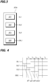
- FIG. 3 is a configuration view illustrating an exemplary embodiment of the gate driver driving the pixels illustrated in FIG. 2 .
- a gate driver 320a includes a first gate circuit 321 connected to a first gate line GL1 to output a first gate signal, a second gate circuit 322 connected to a second gate line GL2 to output a second gate signal, a third gate circuit 323 connected to a third gate line GL3 to output a third gate signal, and an emission control circuit 324 connected to an emission control line EML 1 to output an emission control signal.
- the gate driver 320a is connected to the first pixel 201a and the second pixel 201 b, as described above with reference to FIG. 2 .
- the first pixel 201a may have the first gate signal and the second gate signal delivered thereto through the first gate line GL1 and the second gate line GL2 connected thereto.
- the first pixel 201a may have a reference voltage delivered thereto in response to the first gate signal and may have a data signal delivered thereto in response to the second gate signal.
- the first pixel 201a may have an emission control signal delivered thereto through the emission control line EML1.
- the second pixel 201b may have the second gate signal and a third gate signal delivered thereto through the second gate line GL2 and the third gate line GL3 connected thereto.
- the second pixel 201b may have the emission control signal delivered thereto through the emission control line EML1.
- the first pixel 201a and the second pixel 201b may emit light in response to a single emission control signal.
- the gate driver 320a may deliver three different gate signals and a single emission control signal to two pixels. Since gate signals are sequentially output, even in the case in which three different gate signals are delivered to two pixels, there may be no change in the number of gate circuits outputting gate signals to the gate driver 320a.
- the first pixel 201a and the second pixel 201b receive an emission control signal through a single emission control line EML1, only a single emission control circuit 324 is required to output the emission control signal to the first and second pixels 201a and 201b.
- the number of emission control circuits 324 outputting emission control signals may be required to be lower than the number of the first to third gate circuits 321 to 323. Therefore, the gate driver 320a can be embodied while having a small size.
- the gate driver 320a when the gate driver 320a is implemented as GIP circuits disposed in a non-display area (not shown) of a display panel, the number of the GIP circuits can be reduced, thereby reducing the size of the non-display area of the display panel.
- FIG. 4 is a timing diagram illustrating exemplary signals input to the first pixel 201a and the second pixel 201b illustrated in FIG. 2 .
- a first gate signal gs1 and a second gate signal gs2 delivered through the first gate line GL1 and the second gate line GL2 may be signals delivered in a low state.
- An emission control signal ems1 delivered through the emission control line EML1 may be a signal delivered in a high state.
- the present disclosure is not limited thereto. In a case in which the first gate signal gs1 and the second gate signal gs2 are delivered in a high state, it may be considered that the first gate signal gs1 and the second gate signal gs2 are not delivered. In a case in which the emission control signal ems1 is delivered in a low state, it may be considered that the emission control signal ems1 is not delivered.
- the first pixel 201a may have the first gate signal gs1 delivered thereto through the first gate line GL1 and the second gate signal gs2 delivered thereto through the second gate line GL2.
- the first pixel 201 a may have the emission control signal ems delivered thereto through the emission control line EML1.
- the first transistor M11 is set to be in an on-state by the first gate signal gs1
- the second transistor M21, the third transistor M31, and the sixth transistor M61 are set to be in an on-state by the second gate signal gs2.
- the fourth transistor M41 and the fifth transistor M51 are turned to an off-state by the emission control signal ems1.
- the reference voltage Vref may be delivered to the third node N31.
- the reference voltage Vref may be delivered to the second electrode of the capacitor C11.
- the capacitor C11 may be initialized by the reference voltage Vref.
- a data voltage Vdata may be delivered to the first node N11.
- the third transistor M31 is in an on-state, the voltage of the second node N21 may be substantially the same as the voltage of the third node N31. Accordingly, the driving transistor DT1 electrically connects the nodes N21 and N31, thereby allowing a driving current to flow from the first electrode to the second electrode of the driving transistor DT1.
- the driving current may not flow into the OLED OLED1.
- the sixth transistor M61 since the sixth transistor M61 is in an on-state, the reference voltage Vref may be delivered to the anode of the OLED OLED1. The reference voltage Vref may be lower than the threshold voltage of the OLED OLED1. Therefore, the OLED OLED1 may not emit light.
- the second pixel 201b may have the second gate signal gs2 delivered thereto through the second gate line GL2 and may not have a third gate signal gs3 delivered thereto through the third gate line GL3.
- the second pixel 201b may have the emission control signal ems1 delivered thereto through the emission control line EML1.
- the first transistor M12 of the second pixel 201b may be in an on-state.
- the third gate signal gs3 is not delivered to the second pixel 201b, the second transistor M22, the third transistor M32, and the sixth transistor M62 may be in an off-state.
- the emission control signal ems1 is delivered to the second pixel 201b
- the fifth transistor M42 and the fifth transistor M52 may be in an off-state.
- the reference voltage Vref may be delivered to the third node N32. Therefore, the reference voltage Vref may be delivered to the second electrode of the capacitor C12.
- the capacitor C12 may be initialized by the reference voltage Vref.
- the first gate signal gs1 may not be delivered to the first pixel 201a through the first gate line GL1.
- the first pixel 201a may have the second gate signal gs2 delivered thereto through the second gate line GL2.
- the first pixel 201a may have the emission control signal delivered thereto through the emission control line EML1.
- the first transistor M11 may be in an off-state.
- the second transistor M21, the third transistor M31, and the sixth transistor M61 may be in an on-state.
- the fourth transistor M41 and the fifth transistor M51 may be in an off-state.
- a data voltage Vdata applied to the data line DL1 may be delivered to the first node N11.
- the data voltage Vdata delivered to the first node N11 in the second time period T2 may be different from the data voltage Vdata delivered to the first node N11 in the first time period T1.
- the third transistor M31 of the first pixel 201a is in an on-state, the second node N21 and the third node N31 are connected to allow the driving transistor DT1 to act as a diode, so that a driving current flows from the first electrode to the second electrode of the driving transistor DT1.
- a voltage of the second electrode of the capacitor C11 connected to the third node n31 may correspond to the level of the threshold voltage of the driving transistor DT1.
- the sixth transistor M61 of the first pixel 201a may be in an on-state and the reference voltage Vref may be delivered to the anode of the OLED OLED1 through the reference line VL2 to which the reference voltage Vref is applied, and thus, a voltage of the anode of the OLED OLED1 may be initialized as the reference voltage Vref. Therefore, the second time period T2 may be a time period in which the threshold voltage of the driving transistor DT1 of the first pixel 201a is sensed and the voltage of the anode of the OLED OLED1 is initialized.
- the second pixel 201b may receive the second gate signal gs2 through the second gate line GL2 and the third gate signal gs3 through the third gate line GL3.
- the second pixel 201b may receive the emission control signal ems1 through the emission control line EML1.
- the first transistor M12 is switched to an on-state by the second gate signal gs2, and the second transistor M22, the third transistor M32, and the sixth transistor M62 are set to be in an on-state by the second gate signal gs2.
- the fourth transistor M41 and the fifth transistor M51 may be set to be in an off-state by the emission control signal ems1.
- the reference voltage Vref may be delivered to the third node N32.
- the reference voltage Vref may be delivered to the second electrode of the capacitor C12.
- a data voltage Vdata may be delivered to the first node N12.
- the data voltage Vdata delivered to the first node N12 of the second pixel 201b may be substantially the same as the data voltage Vdata delivered to the first node N11 in the second time period T2.
- the second node N22 and the third node N32 are connected to allow the driving transistor DT2 of the second pixel 201b to act as a diode, so that a driving current flows from the first electrode to the second electrode of the driving transistor DT2.
- the driving current may not flow into the OLED OLED2.
- the reference voltage Vref may be delivered to the anode of the OLED OLED2.
- the reference voltage Vref may be lower than the threshold voltage of the OLED OLED2, and thus, the OLED OLED2 may not emit light.
- the first pixel 201a may not receive the first gate signal gs1 through the first gate line GL1 and the second gate signal gs2 through the second gate line GL2. In addition, the first pixel 201a may receive the emission control signal. Therefore, the first to sixth transistors M11 to M61 of the first pixel 201 a may maintain an off-state.
- the (2-1)th time period T2-1 when the first to sixth transistors M11 to M61 of the first pixel 201 a are in an off-state, the capacitor C11 is in a floating state, so that the data voltage Vdata input to the first electrode of the capacitor C11 in the second time period T2 can be maintained in the (2-1)th time period T2-1. Therefore, the (2-1)th time period T2-1 may be a time period in which the data voltage Vdata is held in the first pixel 201 a.
- the second pixel 201b may not receive the first gate signal gs1 through the first gate line GL1 and may receive the second gate signal gs2 through the second gate line GL2.
- the second pixel 201b may receive the emission control signal through the emission control line EML1.
- the first transistor M12 may be in an off-state.
- the second transistor M22, the third transistor M32, and the sixth transistor M62 may be in an on-state.
- the fourth transistor M42 and the fifth transistor M52 may be set to be in an off-state by the emission control signal ems1.
- the second transistor M22 of the second pixel 201b when the second transistor M22 of the second pixel 201b is in an on-state, a data voltage Vdata is delivered to the first node N12, so that the data voltage Vdata can be delivered to the first electrode of the capacitor C12.
- the data voltage Vdata delivered to the first node N12 in the (2-1)th time period T2-1 may be the data voltage Vdata applied to the data line DL1 in the (2-1)th time period T2-1.
- the third transistor M32 When the third transistor M32 is in an on-state, the second node N22 and the third node N32 are connected, so that a driving current flows from the first electrode to the second electrode of the driving transistor DT2.
- the sixth transistor M62 of the second pixel 201b may be in an on-state and the reference voltage Vref may be delivered to the anode of the OLED OLED2 through the reference line VL2 to which the reference voltage Vref is applied, and thus, a voltage of the anode of the OLED OLED2 may be initialized as the reference voltage Vref. Therefore, the (2-1)th time period T2-1 may be a time period in which a threshold voltage of the driving transistor DT2 of the second pixel 201b is sensed and the voltage of the anode of the OLED OLED2is initialized.
- the first pixel 201a and the second pixel 201b may not receive the first and second gate signals gs1 and gs2 and the second and third gate signals gs2 and gs3, respectively.
- each of the first pixel 201a and the second pixel 201b may not receive the emission control signal through the emission control line EML1.
- the fourth transistor M41 and the fifth transistor M51 may be in an on-state.
- a reference voltage Vref may be delivered to the first node N11.
- a voltage of the first node N11 may be changed from the data voltage Vdata to the reference voltage Vref, and a voltage of the third node N31 may be set to correspond to a difference between the data voltage Vdata and the reference voltage Vref and correspond to the threshold voltage of the driving transistor DT1, in response to a voltage stored the capacitor C11.
- I OLED is a magnitude of a driving current
- ⁇ is a constant
- ELVDD is a voltage of the first power
- V th is the threshold voltage of the driving transistor DT1
- V data is a voltage of a data signal
- V ref is a reference voltage.
- the driving current flowing from the first pixel 201a to the OLED OLED1 in the third time period T3 may be a driving current in which the threshold voltage of the driving transistor DT1 is compensated for.
- the driving current flowing from the second pixel 201b to the OLED OLED2 may be a driving current in which the threshold voltage of the driving transistor DT2 is compensated for.
- points in time at which the first pixel 201a and the second pixel 201b emit light can be controlled by a single emission control signal, so that two adjacent pixels connected to the same data line, as in the gate driver 320a illustrated in FIG. 3 , can receive an emission control signal from a single emission control circuit. Accordingly, the number of the emission control circuits can be reduced to reduce the number and the size of output terminals of the gate driver 320a. In particular, when a holding period in which a data voltage is maintained in the first pixel 201a is set, points in time at which the first pixel 201a and the second pixel 201b emit light can be controlled by a single emission control signal.
- FIG. 5 is a flowchart illustrating a method of driving the organic light-emitting display device illustrated in FIG. 1 , according to exemplary embodiments.
- the method of driving the organic light-emitting display device includes step S500 of initializing two pixels.
- the two pixels may be pixels that are adjacent to each other while being connected to the same data line.
- the two pixels may be pixels to which data signals are input in response to different gate signals.
- the two pixels may be referred to as a first pixel and a second pixel, respectively.
- the first pixel and the second pixel may be sequentially initialized.
- the first pixel may be initialized in response to a first gate signal
- the second pixel may be initialized in response to a second gate signal generated after the first gate signal.
- the initialization may be performed by delivering reference voltages to the first pixel and the second pixel.
- the reference voltages may be the first gate signal and the second gate signal delivered to the first pixel and the second pixel, instead of being separate control signals.
- the method of driving the organic light-emitting display device includes step S510 of sampling the threshold voltages of the two pixels.
- data voltages may be input to the two pixels.
- the sampling of the threshold voltages of the two pixels may be performed such that the sampling time of the first pixel is a different time from the sampling time of the second pixel.
- the threshold voltages of the first pixel and the second pixel may be sequentially sampled using the second gate signal and a third gate signal generated after the second gate signal.
- the threshold voltages to be sampled may be threshold voltages of driving transistors allowing driving currents to flow into the first pixel and the second pixel, respectively.
- data signals may be input to the first pixel and the second pixel.
- the first pixel may receive the data signal input thereto in response to the second gate signal, while the second pixel may receive the data signal input thereto in response to the third gate signal. Since the second gate signal and the third gate signal inputting the data signals during the sampling of the threshold voltages can be used, the threshold voltages of the first pixel and the second pixel can be sampled without using separate signals.
- step S530 the first pixel of the two pixels maintains the data signal input thereto.
- a period of time for which the first pixel maintains the input data signal may be a period of time for which the data signal is being input to the second pixel.
- An emission control signal can be input at the same time, since the first pixel has a period of time for which the received data signal is maintained.
- the two pixels emit light.
- the OLEDs can simultaneously emit light.
- the term "simultaneously” used herein may mean “at the same time” as well as “at slightly different times”.
- the OLEDs may be allowed to emit light in response to a single emission control signal, so that the first pixel and the second pixel can simultaneously emit light. Since the first pixel and the second pixel can emit light in response to a single emission control signal, the number of emission control circuits outputting emission control signals can be reduced. This can consequently reduce the number of circuits outputting signals in the gate driver, thereby allowing the gate driver to be embodied in a small size.
- the gate driver since the first pixel and the second pixel are initialized and sampled using the first to third gate signals, it is unnecessary for the gate driver to output separate signals for the initialization and the sampling. This can consequently reduce the number of circuits outputting signals in the gate driver, thereby allowing the gate driver to be embodied in a small size.
Landscapes
- Engineering & Computer Science (AREA)
- Physics & Mathematics (AREA)
- Computer Hardware Design (AREA)
- General Physics & Mathematics (AREA)
- Theoretical Computer Science (AREA)
- Microelectronics & Electronic Packaging (AREA)
- Control Of Indicators Other Than Cathode Ray Tubes (AREA)
- Control Of El Displays (AREA)
- Electroluminescent Light Sources (AREA)
Applications Claiming Priority (1)
| Application Number | Priority Date | Filing Date | Title |
|---|---|---|---|
| KR1020160180716A KR102573334B1 (ko) | 2016-12-28 | 2016-12-28 | 유기발광표시장치 및 그의 구동방법 |
Publications (3)
| Publication Number | Publication Date |
|---|---|
| EP3343557A2 true EP3343557A2 (de) | 2018-07-04 |
| EP3343557A3 EP3343557A3 (de) | 2018-11-14 |
| EP3343557B1 EP3343557B1 (de) | 2024-04-10 |
Family
ID=60673783
Family Applications (1)
| Application Number | Title | Priority Date | Filing Date |
|---|---|---|---|
| EP17207918.8A Active EP3343557B1 (de) | 2016-12-28 | 2017-12-18 | Organische lichtemittierende anzeigevorrichtung und ansteuerungsverfahren dafür |
Country Status (4)
| Country | Link |
|---|---|
| US (1) | US10510293B2 (de) |
| EP (1) | EP3343557B1 (de) |
| KR (1) | KR102573334B1 (de) |
| CN (1) | CN108257552B (de) |
Families Citing this family (24)
| Publication number | Priority date | Publication date | Assignee | Title |
|---|---|---|---|---|
| KR102382323B1 (ko) * | 2015-09-30 | 2022-04-05 | 엘지디스플레이 주식회사 | 유기발광다이오드 표시장치 |
| CN106531074B (zh) * | 2017-01-10 | 2019-02-05 | 上海天马有机发光显示技术有限公司 | 有机发光像素驱动电路、驱动方法以及有机发光显示面板 |
| KR102775758B1 (ko) | 2017-02-24 | 2025-03-07 | 삼성디스플레이 주식회사 | 화소 및 이를 가지는 유기전계발광 표시장치 |
| EP3493189B1 (de) | 2017-11-30 | 2023-08-30 | LG Display Co., Ltd. | Elektrolumineszente anzeigevorrichtung |
| CN118675469A (zh) | 2018-09-13 | 2024-09-20 | 京东方科技集团股份有限公司 | 像素电路及其驱动方法、显示装置 |
| KR102542606B1 (ko) * | 2018-09-21 | 2023-06-15 | 삼성디스플레이 주식회사 | 화소 및 이를 포함하는 표시 장치 |
| KR102706596B1 (ko) * | 2018-12-28 | 2024-09-12 | 엘지디스플레이 주식회사 | 발광 표시장치 |
| CN109961738A (zh) * | 2019-04-04 | 2019-07-02 | 深圳市华星光电半导体显示技术有限公司 | 像素驱动电路以及显示面板 |
| KR102751621B1 (ko) * | 2019-06-18 | 2025-01-10 | 삼성디스플레이 주식회사 | 표시 장치 및 이의 구동 방법 |
| KR102772206B1 (ko) * | 2019-07-26 | 2025-02-26 | 삼성디스플레이 주식회사 | 표시 장치 및 이의 구동 방법 |
| EP4016510B1 (de) * | 2019-08-14 | 2024-04-10 | BOE Technology Group Co., Ltd. | Pixelschaltung und ansteuerungsverfahren dafür, arraysubstrat und anzeigevorrichtung |
| KR102618390B1 (ko) * | 2019-10-04 | 2023-12-27 | 엘지디스플레이 주식회사 | 표시장치와 그 구동 방법 |
| CN110890066B (zh) * | 2019-11-26 | 2021-08-03 | 深圳市华星光电半导体显示技术有限公司 | 一种子像素电路、像素电路及显示装置 |
| KR102667950B1 (ko) * | 2019-12-24 | 2024-05-21 | 엘지디스플레이 주식회사 | 유기 전계발광 표시장치 및 그의 구동방법 |
| CN111063301B (zh) * | 2020-01-09 | 2024-04-12 | 京东方科技集团股份有限公司 | 像素电路及其驱动方法、阵列基板及显示装置 |
| CN111477174A (zh) * | 2020-04-23 | 2020-07-31 | 京东方科技集团股份有限公司 | 像素电路及其驱动方法、显示基板 |
| CN111583872B (zh) * | 2020-06-11 | 2021-03-12 | 京东方科技集团股份有限公司 | 像素补偿装置及像素补偿方法、显示装置 |
| CN112037716B (zh) * | 2020-09-21 | 2022-01-21 | 京东方科技集团股份有限公司 | 像素电路、显示面板和显示设备 |
| KR102906255B1 (ko) * | 2020-11-09 | 2025-12-30 | 엘지디스플레이 주식회사 | 발광표시패널 및 이를 이용한 발광표시장치 |
| KR102740141B1 (ko) * | 2020-12-24 | 2024-12-06 | 엘지디스플레이 주식회사 | 듀얼 데이터배선을 포함하는 표시장치 및 그 구동방법 |
| KR102765887B1 (ko) * | 2020-12-29 | 2025-02-07 | 엘지디스플레이 주식회사 | 먹스를 포함하는 표시장치 및 그 구동방법 |
| CN113506540A (zh) * | 2021-06-09 | 2021-10-15 | 深圳职业技术学院 | 一种利于高阶显示的像素电路 |
| KR102751107B1 (ko) * | 2022-05-31 | 2025-01-06 | 엘지디스플레이 주식회사 | 화소 회로 및 화소 회로를 포함하는 표시 장치 |
| CN115440162B (zh) | 2022-11-09 | 2023-03-24 | 惠科股份有限公司 | 显示面板及显示装置 |
Family Cites Families (30)
| Publication number | Priority date | Publication date | Assignee | Title |
|---|---|---|---|---|
| KR100583519B1 (ko) * | 2004-10-28 | 2006-05-25 | 삼성에스디아이 주식회사 | 주사 구동부 및 그를 이용한 발광표시장치 |
| KR100662998B1 (ko) * | 2005-11-04 | 2006-12-28 | 삼성에스디아이 주식회사 | 유기 전계발광 표시장치 및 그 구동방법 |
| KR101359921B1 (ko) * | 2007-03-02 | 2014-02-07 | 삼성디스플레이 주식회사 | 표시 장치 |
| KR20090105630A (ko) * | 2008-04-03 | 2009-10-07 | 삼성전자주식회사 | 전기 영동 표시 장치 및 그 구동 방법 |
| KR101058115B1 (ko) | 2009-11-16 | 2011-08-24 | 삼성모바일디스플레이주식회사 | 화소 회로, 유기 전계 발광 표시 장치 |
| KR101048919B1 (ko) | 2010-02-17 | 2011-07-12 | 삼성모바일디스플레이주식회사 | 유기전계발광 표시장치 |
| JP5630203B2 (ja) * | 2010-10-21 | 2014-11-26 | セイコーエプソン株式会社 | 電気光学装置、および電子機器。 |
| KR101838047B1 (ko) * | 2011-07-05 | 2018-03-14 | 엘지디스플레이 주식회사 | 전기영동 표시장치와 이의 구동방법 |
| KR101920492B1 (ko) * | 2011-09-20 | 2018-11-22 | 엘지디스플레이 주식회사 | 유기발광다이오드 표시장치 |
| TWI565048B (zh) | 2012-05-22 | 2017-01-01 | 友達光電股份有限公司 | 有機發光顯示單元結構與有機發光顯示單元電路 |
| KR101360767B1 (ko) * | 2012-08-17 | 2014-02-12 | 엘지디스플레이 주식회사 | 유기 발광 다이오드 표시장치 및 그 구동 방법 |
| KR102077661B1 (ko) | 2013-05-07 | 2020-02-17 | 삼성디스플레이 주식회사 | 유기 발광 표시 장치 및 그 구동 방법 |
| CN103268753A (zh) * | 2013-05-28 | 2013-08-28 | 上海中科高等研究院 | 扫描线共用的amoled驱动电路及其驱动方法 |
| US9454935B2 (en) * | 2013-11-21 | 2016-09-27 | Lg Display Co., Ltd. | Organic light emitting diode display device |
| CN203982747U (zh) * | 2014-05-20 | 2014-12-03 | 华南理工大学 | 有源有机电致发光显示器的像素电路 |
| KR102257941B1 (ko) * | 2014-06-17 | 2021-05-31 | 삼성디스플레이 주식회사 | 유기 발광 표시 장치 |
| US9805652B2 (en) * | 2014-07-29 | 2017-10-31 | Lg Display Co., Ltd. | Organic light emitting display device and method of driving the same |
| KR20160053050A (ko) * | 2014-10-30 | 2016-05-13 | 삼성디스플레이 주식회사 | 화소 및 이를 포함하는 유기발광표시장치 |
| CN104575379B (zh) * | 2014-12-26 | 2018-01-16 | 北京大学深圳研究生院 | 显示装置及其驱动方法 |
| KR102265368B1 (ko) * | 2015-01-13 | 2021-06-15 | 삼성디스플레이 주식회사 | 화소, 이를 포함하는 표시 장치 및 그 구동방법 |
| KR102357390B1 (ko) | 2015-02-09 | 2022-02-03 | 삼성디스플레이 주식회사 | 유기 발광 표시 장치 및 그 구동 방법 |
| KR102516643B1 (ko) | 2015-04-30 | 2023-04-04 | 삼성디스플레이 주식회사 | 화소 및 이를 이용한 유기전계발광 표시장치 |
| EP3098804A3 (de) * | 2015-05-28 | 2016-12-21 | LG Display Co., Ltd. | Organische lichtemittierende anzeige |
| CN104992674A (zh) | 2015-07-24 | 2015-10-21 | 上海和辉光电有限公司 | 一种像素补偿电路 |
| KR102503160B1 (ko) * | 2015-09-30 | 2023-02-24 | 엘지디스플레이 주식회사 | 유기발광다이오드 표시장치 |
| CN106782328A (zh) * | 2015-11-20 | 2017-05-31 | 上海和辉光电有限公司 | 一种像素电路 |
| KR102597752B1 (ko) | 2015-12-01 | 2023-11-07 | 엘지디스플레이 주식회사 | 유기발광다이오드 표시장치 |
| US10262586B2 (en) * | 2016-03-14 | 2019-04-16 | Apple Inc. | Light-emitting diode display with threshold voltage compensation |
| CN105632409B (zh) * | 2016-03-23 | 2018-10-12 | 信利(惠州)智能显示有限公司 | 有机显示面板像素驱动方法及电路 |
| KR102773736B1 (ko) * | 2016-11-30 | 2025-02-27 | 엘지디스플레이 주식회사 | 유기 발광 다이오드 표시 장치 |
-
2016
- 2016-12-28 KR KR1020160180716A patent/KR102573334B1/ko active Active
-
2017
- 2017-11-30 US US15/828,032 patent/US10510293B2/en active Active
- 2017-12-04 CN CN201711280462.3A patent/CN108257552B/zh active Active
- 2017-12-18 EP EP17207918.8A patent/EP3343557B1/de active Active
Also Published As
| Publication number | Publication date |
|---|---|
| US10510293B2 (en) | 2019-12-17 |
| KR20180077353A (ko) | 2018-07-09 |
| CN108257552B (zh) | 2021-01-26 |
| KR102573334B1 (ko) | 2023-09-01 |
| US20180182289A1 (en) | 2018-06-28 |
| EP3343557B1 (de) | 2024-04-10 |
| EP3343557A3 (de) | 2018-11-14 |
| CN108257552A (zh) | 2018-07-06 |
Similar Documents
| Publication | Publication Date | Title |
|---|---|---|
| EP3343557B1 (de) | Organische lichtemittierende anzeigevorrichtung und ansteuerungsverfahren dafür | |
| EP3863006B1 (de) | Anzeigevorrichtung mit konfiguration zur konstantstromeinstellung und ansteuerungsverfahren dafür | |
| KR101097325B1 (ko) | 화소 회로 및 유기 전계 발광 표시 장치 | |
| US10872562B2 (en) | Pixel and organic light emitting display device including the same | |
| KR101058115B1 (ko) | 화소 회로, 유기 전계 발광 표시 장치 | |
| US8736523B2 (en) | Pixel circuit configured to perform initialization and compensation at different time periods and organic electroluminescent display including the same | |
| JP4657580B2 (ja) | 表示装置及びその駆動方法 | |
| KR101127582B1 (ko) | 화소 회로, 유기 전계 발광 표시 장치 및 그 구동 방법 | |
| US11081056B2 (en) | Organic light emitting display device and driving method thereof | |
| KR102461361B1 (ko) | 화소, 화소의 구동방법 및 화소를 포함하는 유기발광 표시장치 | |
| US10839754B2 (en) | Organic light emitting display having multiplexer for distributing data voltages | |
| US9792853B2 (en) | Pixel, driving method of pixel, and display device including pixel | |
| KR102352282B1 (ko) | 유기 발광 표시 장치 | |
| US9129560B2 (en) | Display device | |
| US9601056B2 (en) | Pixel and organic light emitting display device using the same | |
| KR20160090975A (ko) | 표시 장치 및 그 구동 방법 | |
| JP2005141195A (ja) | 画像表示装置及びその駆動方法 | |
| KR102397982B1 (ko) | 화소 및 이를 포함하는 유기발광 표시장치 | |
| KR20210085628A (ko) | 유기발광 표시장치와 그 구동방법 | |
| KR20090116402A (ko) | 표시 장치 | |
| US12190810B2 (en) | Pixel circuit, display device, and driving method | |
| US10460665B2 (en) | OLED pixel driving circuit and driving method thereof | |
| KR20050112841A (ko) | 전하 펌핑 회로, 이를 이용한 전원공급장치 및 표시 장치 |
Legal Events
| Date | Code | Title | Description |
|---|---|---|---|
| PUAI | Public reference made under article 153(3) epc to a published international application that has entered the european phase |
Free format text: ORIGINAL CODE: 0009012 |
|
| STAA | Information on the status of an ep patent application or granted ep patent |
Free format text: STATUS: REQUEST FOR EXAMINATION WAS MADE |
|
| 17P | Request for examination filed |
Effective date: 20171218 |
|
| AK | Designated contracting states |
Kind code of ref document: A2 Designated state(s): AL AT BE BG CH CY CZ DE DK EE ES FI FR GB GR HR HU IE IS IT LI LT LU LV MC MK MT NL NO PL PT RO RS SE SI SK SM TR |
|
| AX | Request for extension of the european patent |
Extension state: BA ME |
|
| PUAL | Search report despatched |
Free format text: ORIGINAL CODE: 0009013 |
|
| AK | Designated contracting states |
Kind code of ref document: A3 Designated state(s): AL AT BE BG CH CY CZ DE DK EE ES FI FR GB GR HR HU IE IS IT LI LT LU LV MC MK MT NL NO PL PT RO RS SE SI SK SM TR |
|
| AX | Request for extension of the european patent |
Extension state: BA ME |
|
| RIC1 | Information provided on ipc code assigned before grant |
Ipc: G09G 3/3233 20160101AFI20181005BHEP |
|
| RBV | Designated contracting states (corrected) |
Designated state(s): AL AT BE BG CH CY CZ DE DK EE ES FI FR GB GR HR HU IE IS IT LI LT LU LV MC MK MT NL NO PL PT RO RS SE SI SK SM TR |
|
| STAA | Information on the status of an ep patent application or granted ep patent |
Free format text: STATUS: EXAMINATION IS IN PROGRESS |
|
| 17Q | First examination report despatched |
Effective date: 20210210 |
|
| GRAP | Despatch of communication of intention to grant a patent |
Free format text: ORIGINAL CODE: EPIDOSNIGR1 |
|
| STAA | Information on the status of an ep patent application or granted ep patent |
Free format text: STATUS: GRANT OF PATENT IS INTENDED |
|
| INTG | Intention to grant announced |
Effective date: 20231108 |
|
| GRAS | Grant fee paid |
Free format text: ORIGINAL CODE: EPIDOSNIGR3 |
|
| GRAA | (expected) grant |
Free format text: ORIGINAL CODE: 0009210 |
|
| STAA | Information on the status of an ep patent application or granted ep patent |
Free format text: STATUS: THE PATENT HAS BEEN GRANTED |
|
| AK | Designated contracting states |
Kind code of ref document: B1 Designated state(s): AL AT BE BG CH CY CZ DE DK EE ES FI FR GB GR HR HU IE IS IT LI LT LU LV MC MK MT NL NO PL PT RO RS SE SI SK SM TR |
|
| REG | Reference to a national code |
Ref country code: GB Ref legal event code: FG4D |
|
| REG | Reference to a national code |
Ref country code: CH Ref legal event code: EP |
|
| REG | Reference to a national code |
Ref country code: DE Ref legal event code: R096 Ref document number: 602017080803 Country of ref document: DE |
|
| REG | Reference to a national code |
Ref country code: IE Ref legal event code: FG4D |
|
| REG | Reference to a national code |
Ref country code: LT Ref legal event code: MG9D |
|
| REG | Reference to a national code |
Ref country code: NL Ref legal event code: MP Effective date: 20240410 |
|
| REG | Reference to a national code |
Ref country code: AT Ref legal event code: MK05 Ref document number: 1675725 Country of ref document: AT Kind code of ref document: T Effective date: 20240410 |
|
| PG25 | Lapsed in a contracting state [announced via postgrant information from national office to epo] |
Ref country code: NL Free format text: LAPSE BECAUSE OF FAILURE TO SUBMIT A TRANSLATION OF THE DESCRIPTION OR TO PAY THE FEE WITHIN THE PRESCRIBED TIME-LIMIT Effective date: 20240410 |
|
| PG25 | Lapsed in a contracting state [announced via postgrant information from national office to epo] |
Ref country code: NL Free format text: LAPSE BECAUSE OF FAILURE TO SUBMIT A TRANSLATION OF THE DESCRIPTION OR TO PAY THE FEE WITHIN THE PRESCRIBED TIME-LIMIT Effective date: 20240410 |
|
| PG25 | Lapsed in a contracting state [announced via postgrant information from national office to epo] |
Ref country code: IS Free format text: LAPSE BECAUSE OF FAILURE TO SUBMIT A TRANSLATION OF THE DESCRIPTION OR TO PAY THE FEE WITHIN THE PRESCRIBED TIME-LIMIT Effective date: 20240810 |
|
| PG25 | Lapsed in a contracting state [announced via postgrant information from national office to epo] |
Ref country code: BG Free format text: LAPSE BECAUSE OF FAILURE TO SUBMIT A TRANSLATION OF THE DESCRIPTION OR TO PAY THE FEE WITHIN THE PRESCRIBED TIME-LIMIT Effective date: 20240410 |
|
| PG25 | Lapsed in a contracting state [announced via postgrant information from national office to epo] |
Ref country code: FI Free format text: LAPSE BECAUSE OF FAILURE TO SUBMIT A TRANSLATION OF THE DESCRIPTION OR TO PAY THE FEE WITHIN THE PRESCRIBED TIME-LIMIT Effective date: 20240410 Ref country code: HR Free format text: LAPSE BECAUSE OF FAILURE TO SUBMIT A TRANSLATION OF THE DESCRIPTION OR TO PAY THE FEE WITHIN THE PRESCRIBED TIME-LIMIT Effective date: 20240410 |
|
| PG25 | Lapsed in a contracting state [announced via postgrant information from national office to epo] |
Ref country code: GR Free format text: LAPSE BECAUSE OF FAILURE TO SUBMIT A TRANSLATION OF THE DESCRIPTION OR TO PAY THE FEE WITHIN THE PRESCRIBED TIME-LIMIT Effective date: 20240711 |
|
| PG25 | Lapsed in a contracting state [announced via postgrant information from national office to epo] |
Ref country code: PT Free format text: LAPSE BECAUSE OF FAILURE TO SUBMIT A TRANSLATION OF THE DESCRIPTION OR TO PAY THE FEE WITHIN THE PRESCRIBED TIME-LIMIT Effective date: 20240812 |
|
| PG25 | Lapsed in a contracting state [announced via postgrant information from national office to epo] |
Ref country code: ES Free format text: LAPSE BECAUSE OF FAILURE TO SUBMIT A TRANSLATION OF THE DESCRIPTION OR TO PAY THE FEE WITHIN THE PRESCRIBED TIME-LIMIT Effective date: 20240410 |
|
| PG25 | Lapsed in a contracting state [announced via postgrant information from national office to epo] |
Ref country code: AT Free format text: LAPSE BECAUSE OF FAILURE TO SUBMIT A TRANSLATION OF THE DESCRIPTION OR TO PAY THE FEE WITHIN THE PRESCRIBED TIME-LIMIT Effective date: 20240410 |
|
| PG25 | Lapsed in a contracting state [announced via postgrant information from national office to epo] |
Ref country code: PL Free format text: LAPSE BECAUSE OF FAILURE TO SUBMIT A TRANSLATION OF THE DESCRIPTION OR TO PAY THE FEE WITHIN THE PRESCRIBED TIME-LIMIT Effective date: 20240410 |
|
| PG25 | Lapsed in a contracting state [announced via postgrant information from national office to epo] |
Ref country code: LV Free format text: LAPSE BECAUSE OF FAILURE TO SUBMIT A TRANSLATION OF THE DESCRIPTION OR TO PAY THE FEE WITHIN THE PRESCRIBED TIME-LIMIT Effective date: 20240410 |
|
| PG25 | Lapsed in a contracting state [announced via postgrant information from national office to epo] |
Ref country code: PT Free format text: LAPSE BECAUSE OF FAILURE TO SUBMIT A TRANSLATION OF THE DESCRIPTION OR TO PAY THE FEE WITHIN THE PRESCRIBED TIME-LIMIT Effective date: 20240812 Ref country code: PL Free format text: LAPSE BECAUSE OF FAILURE TO SUBMIT A TRANSLATION OF THE DESCRIPTION OR TO PAY THE FEE WITHIN THE PRESCRIBED TIME-LIMIT Effective date: 20240410 Ref country code: NO Free format text: LAPSE BECAUSE OF FAILURE TO SUBMIT A TRANSLATION OF THE DESCRIPTION OR TO PAY THE FEE WITHIN THE PRESCRIBED TIME-LIMIT Effective date: 20240710 Ref country code: LV Free format text: LAPSE BECAUSE OF FAILURE TO SUBMIT A TRANSLATION OF THE DESCRIPTION OR TO PAY THE FEE WITHIN THE PRESCRIBED TIME-LIMIT Effective date: 20240410 Ref country code: IS Free format text: LAPSE BECAUSE OF FAILURE TO SUBMIT A TRANSLATION OF THE DESCRIPTION OR TO PAY THE FEE WITHIN THE PRESCRIBED TIME-LIMIT Effective date: 20240810 Ref country code: HR Free format text: LAPSE BECAUSE OF FAILURE TO SUBMIT A TRANSLATION OF THE DESCRIPTION OR TO PAY THE FEE WITHIN THE PRESCRIBED TIME-LIMIT Effective date: 20240410 Ref country code: GR Free format text: LAPSE BECAUSE OF FAILURE TO SUBMIT A TRANSLATION OF THE DESCRIPTION OR TO PAY THE FEE WITHIN THE PRESCRIBED TIME-LIMIT Effective date: 20240711 Ref country code: FI Free format text: LAPSE BECAUSE OF FAILURE TO SUBMIT A TRANSLATION OF THE DESCRIPTION OR TO PAY THE FEE WITHIN THE PRESCRIBED TIME-LIMIT Effective date: 20240410 Ref country code: ES Free format text: LAPSE BECAUSE OF FAILURE TO SUBMIT A TRANSLATION OF THE DESCRIPTION OR TO PAY THE FEE WITHIN THE PRESCRIBED TIME-LIMIT Effective date: 20240410 Ref country code: BG Free format text: LAPSE BECAUSE OF FAILURE TO SUBMIT A TRANSLATION OF THE DESCRIPTION OR TO PAY THE FEE WITHIN THE PRESCRIBED TIME-LIMIT Effective date: 20240410 Ref country code: AT Free format text: LAPSE BECAUSE OF FAILURE TO SUBMIT A TRANSLATION OF THE DESCRIPTION OR TO PAY THE FEE WITHIN THE PRESCRIBED TIME-LIMIT Effective date: 20240410 Ref country code: RS Free format text: LAPSE BECAUSE OF FAILURE TO SUBMIT A TRANSLATION OF THE DESCRIPTION OR TO PAY THE FEE WITHIN THE PRESCRIBED TIME-LIMIT Effective date: 20240710 |
|
| REG | Reference to a national code |
Ref country code: DE Ref legal event code: R097 Ref document number: 602017080803 Country of ref document: DE |
|
| PG25 | Lapsed in a contracting state [announced via postgrant information from national office to epo] |
Ref country code: DK Free format text: LAPSE BECAUSE OF FAILURE TO SUBMIT A TRANSLATION OF THE DESCRIPTION OR TO PAY THE FEE WITHIN THE PRESCRIBED TIME-LIMIT Effective date: 20240410 |
|
| PG25 | Lapsed in a contracting state [announced via postgrant information from national office to epo] |
Ref country code: EE Free format text: LAPSE BECAUSE OF FAILURE TO SUBMIT A TRANSLATION OF THE DESCRIPTION OR TO PAY THE FEE WITHIN THE PRESCRIBED TIME-LIMIT Effective date: 20240410 |
|
| PG25 | Lapsed in a contracting state [announced via postgrant information from national office to epo] |
Ref country code: CZ Free format text: LAPSE BECAUSE OF FAILURE TO SUBMIT A TRANSLATION OF THE DESCRIPTION OR TO PAY THE FEE WITHIN THE PRESCRIBED TIME-LIMIT Effective date: 20240410 |
|
| PG25 | Lapsed in a contracting state [announced via postgrant information from national office to epo] |
Ref country code: RO Free format text: LAPSE BECAUSE OF FAILURE TO SUBMIT A TRANSLATION OF THE DESCRIPTION OR TO PAY THE FEE WITHIN THE PRESCRIBED TIME-LIMIT Effective date: 20240410 Ref country code: SK Free format text: LAPSE BECAUSE OF FAILURE TO SUBMIT A TRANSLATION OF THE DESCRIPTION OR TO PAY THE FEE WITHIN THE PRESCRIBED TIME-LIMIT Effective date: 20240410 |
|
| PG25 | Lapsed in a contracting state [announced via postgrant information from national office to epo] |
Ref country code: SM Free format text: LAPSE BECAUSE OF FAILURE TO SUBMIT A TRANSLATION OF THE DESCRIPTION OR TO PAY THE FEE WITHIN THE PRESCRIBED TIME-LIMIT Effective date: 20240410 |
|
| PG25 | Lapsed in a contracting state [announced via postgrant information from national office to epo] |
Ref country code: SM Free format text: LAPSE BECAUSE OF FAILURE TO SUBMIT A TRANSLATION OF THE DESCRIPTION OR TO PAY THE FEE WITHIN THE PRESCRIBED TIME-LIMIT Effective date: 20240410 Ref country code: SK Free format text: LAPSE BECAUSE OF FAILURE TO SUBMIT A TRANSLATION OF THE DESCRIPTION OR TO PAY THE FEE WITHIN THE PRESCRIBED TIME-LIMIT Effective date: 20240410 Ref country code: RO Free format text: LAPSE BECAUSE OF FAILURE TO SUBMIT A TRANSLATION OF THE DESCRIPTION OR TO PAY THE FEE WITHIN THE PRESCRIBED TIME-LIMIT Effective date: 20240410 Ref country code: EE Free format text: LAPSE BECAUSE OF FAILURE TO SUBMIT A TRANSLATION OF THE DESCRIPTION OR TO PAY THE FEE WITHIN THE PRESCRIBED TIME-LIMIT Effective date: 20240410 Ref country code: DK Free format text: LAPSE BECAUSE OF FAILURE TO SUBMIT A TRANSLATION OF THE DESCRIPTION OR TO PAY THE FEE WITHIN THE PRESCRIBED TIME-LIMIT Effective date: 20240410 Ref country code: CZ Free format text: LAPSE BECAUSE OF FAILURE TO SUBMIT A TRANSLATION OF THE DESCRIPTION OR TO PAY THE FEE WITHIN THE PRESCRIBED TIME-LIMIT Effective date: 20240410 |
|
| PG25 | Lapsed in a contracting state [announced via postgrant information from national office to epo] |
Ref country code: IT Free format text: LAPSE BECAUSE OF FAILURE TO SUBMIT A TRANSLATION OF THE DESCRIPTION OR TO PAY THE FEE WITHIN THE PRESCRIBED TIME-LIMIT Effective date: 20240410 |
|
| PLBE | No opposition filed within time limit |
Free format text: ORIGINAL CODE: 0009261 |
|
| STAA | Information on the status of an ep patent application or granted ep patent |
Free format text: STATUS: NO OPPOSITION FILED WITHIN TIME LIMIT |
|
| 26N | No opposition filed |
Effective date: 20250113 |
|
| PG25 | Lapsed in a contracting state [announced via postgrant information from national office to epo] |
Ref country code: SI Free format text: LAPSE BECAUSE OF FAILURE TO SUBMIT A TRANSLATION OF THE DESCRIPTION OR TO PAY THE FEE WITHIN THE PRESCRIBED TIME-LIMIT Effective date: 20240410 |
|
| PG25 | Lapsed in a contracting state [announced via postgrant information from national office to epo] |
Ref country code: MC Free format text: LAPSE BECAUSE OF FAILURE TO SUBMIT A TRANSLATION OF THE DESCRIPTION OR TO PAY THE FEE WITHIN THE PRESCRIBED TIME-LIMIT Effective date: 20240410 |
|
| REG | Reference to a national code |
Ref country code: CH Ref legal event code: PL |
|
| PG25 | Lapsed in a contracting state [announced via postgrant information from national office to epo] |
Ref country code: LU Free format text: LAPSE BECAUSE OF NON-PAYMENT OF DUE FEES Effective date: 20241218 |
|
| PG25 | Lapsed in a contracting state [announced via postgrant information from national office to epo] |
Ref country code: SE Free format text: LAPSE BECAUSE OF FAILURE TO SUBMIT A TRANSLATION OF THE DESCRIPTION OR TO PAY THE FEE WITHIN THE PRESCRIBED TIME-LIMIT Effective date: 20240410 |
|
| REG | Reference to a national code |
Ref country code: BE Ref legal event code: MM Effective date: 20241231 |
|
| PG25 | Lapsed in a contracting state [announced via postgrant information from national office to epo] |
Ref country code: BE Free format text: LAPSE BECAUSE OF NON-PAYMENT OF DUE FEES Effective date: 20241231 |
|
| PG25 | Lapsed in a contracting state [announced via postgrant information from national office to epo] |
Ref country code: CH Free format text: LAPSE BECAUSE OF NON-PAYMENT OF DUE FEES Effective date: 20241231 |
|
| PG25 | Lapsed in a contracting state [announced via postgrant information from national office to epo] |
Ref country code: IE Free format text: LAPSE BECAUSE OF NON-PAYMENT OF DUE FEES Effective date: 20241218 |
|
| PGFP | Annual fee paid to national office [announced via postgrant information from national office to epo] |
Ref country code: DE Payment date: 20251020 Year of fee payment: 9 |
|
| PGFP | Annual fee paid to national office [announced via postgrant information from national office to epo] |
Ref country code: GB Payment date: 20251023 Year of fee payment: 9 |
|
| PGFP | Annual fee paid to national office [announced via postgrant information from national office to epo] |
Ref country code: FR Payment date: 20251021 Year of fee payment: 9 |