EP3493189B1 - Elektrolumineszente anzeigevorrichtung - Google Patents
Elektrolumineszente anzeigevorrichtung Download PDFInfo
- Publication number
- EP3493189B1 EP3493189B1 EP18182401.2A EP18182401A EP3493189B1 EP 3493189 B1 EP3493189 B1 EP 3493189B1 EP 18182401 A EP18182401 A EP 18182401A EP 3493189 B1 EP3493189 B1 EP 3493189B1
- Authority
- EP
- European Patent Office
- Prior art keywords
- transistor
- voltage
- node
- gate
- scan
- Prior art date
- Legal status (The legal status is an assumption and is not a legal conclusion. Google has not performed a legal analysis and makes no representation as to the accuracy of the status listed.)
- Active
Links
Images
















Classifications
-
- G—PHYSICS
- G09—EDUCATION; CRYPTOGRAPHY; DISPLAY; ADVERTISING; SEALS
- G09G—ARRANGEMENTS OR CIRCUITS FOR CONTROL OF INDICATING DEVICES USING STATIC MEANS TO PRESENT VARIABLE INFORMATION
- G09G3/00—Control arrangements or circuits, of interest only in connection with visual indicators other than cathode-ray tubes
- G09G3/20—Control arrangements or circuits, of interest only in connection with visual indicators other than cathode-ray tubes for presentation of an assembly of a number of characters, e.g. a page, by composing the assembly by combination of individual elements arranged in a matrix no fixed position being assigned to or needed to be assigned to the individual characters or partial characters
- G09G3/22—Control arrangements or circuits, of interest only in connection with visual indicators other than cathode-ray tubes for presentation of an assembly of a number of characters, e.g. a page, by composing the assembly by combination of individual elements arranged in a matrix no fixed position being assigned to or needed to be assigned to the individual characters or partial characters using controlled light sources
- G09G3/30—Control arrangements or circuits, of interest only in connection with visual indicators other than cathode-ray tubes for presentation of an assembly of a number of characters, e.g. a page, by composing the assembly by combination of individual elements arranged in a matrix no fixed position being assigned to or needed to be assigned to the individual characters or partial characters using controlled light sources using electroluminescent panels
- G09G3/32—Control arrangements or circuits, of interest only in connection with visual indicators other than cathode-ray tubes for presentation of an assembly of a number of characters, e.g. a page, by composing the assembly by combination of individual elements arranged in a matrix no fixed position being assigned to or needed to be assigned to the individual characters or partial characters using controlled light sources using electroluminescent panels semiconductive, e.g. using light-emitting diodes [LED]
- G09G3/3208—Control arrangements or circuits, of interest only in connection with visual indicators other than cathode-ray tubes for presentation of an assembly of a number of characters, e.g. a page, by composing the assembly by combination of individual elements arranged in a matrix no fixed position being assigned to or needed to be assigned to the individual characters or partial characters using controlled light sources using electroluminescent panels semiconductive, e.g. using light-emitting diodes [LED] organic, e.g. using organic light-emitting diodes [OLED]
- G09G3/3225—Control arrangements or circuits, of interest only in connection with visual indicators other than cathode-ray tubes for presentation of an assembly of a number of characters, e.g. a page, by composing the assembly by combination of individual elements arranged in a matrix no fixed position being assigned to or needed to be assigned to the individual characters or partial characters using controlled light sources using electroluminescent panels semiconductive, e.g. using light-emitting diodes [LED] organic, e.g. using organic light-emitting diodes [OLED] using an active matrix
- G09G3/3258—Control arrangements or circuits, of interest only in connection with visual indicators other than cathode-ray tubes for presentation of an assembly of a number of characters, e.g. a page, by composing the assembly by combination of individual elements arranged in a matrix no fixed position being assigned to or needed to be assigned to the individual characters or partial characters using controlled light sources using electroluminescent panels semiconductive, e.g. using light-emitting diodes [LED] organic, e.g. using organic light-emitting diodes [OLED] using an active matrix with pixel circuitry controlling the voltage across the light-emitting element
-
- G—PHYSICS
- G09—EDUCATION; CRYPTOGRAPHY; DISPLAY; ADVERTISING; SEALS
- G09G—ARRANGEMENTS OR CIRCUITS FOR CONTROL OF INDICATING DEVICES USING STATIC MEANS TO PRESENT VARIABLE INFORMATION
- G09G3/00—Control arrangements or circuits, of interest only in connection with visual indicators other than cathode-ray tubes
- G09G3/20—Control arrangements or circuits, of interest only in connection with visual indicators other than cathode-ray tubes for presentation of an assembly of a number of characters, e.g. a page, by composing the assembly by combination of individual elements arranged in a matrix no fixed position being assigned to or needed to be assigned to the individual characters or partial characters
- G09G3/22—Control arrangements or circuits, of interest only in connection with visual indicators other than cathode-ray tubes for presentation of an assembly of a number of characters, e.g. a page, by composing the assembly by combination of individual elements arranged in a matrix no fixed position being assigned to or needed to be assigned to the individual characters or partial characters using controlled light sources
- G09G3/30—Control arrangements or circuits, of interest only in connection with visual indicators other than cathode-ray tubes for presentation of an assembly of a number of characters, e.g. a page, by composing the assembly by combination of individual elements arranged in a matrix no fixed position being assigned to or needed to be assigned to the individual characters or partial characters using controlled light sources using electroluminescent panels
- G09G3/32—Control arrangements or circuits, of interest only in connection with visual indicators other than cathode-ray tubes for presentation of an assembly of a number of characters, e.g. a page, by composing the assembly by combination of individual elements arranged in a matrix no fixed position being assigned to or needed to be assigned to the individual characters or partial characters using controlled light sources using electroluminescent panels semiconductive, e.g. using light-emitting diodes [LED]
- G09G3/3208—Control arrangements or circuits, of interest only in connection with visual indicators other than cathode-ray tubes for presentation of an assembly of a number of characters, e.g. a page, by composing the assembly by combination of individual elements arranged in a matrix no fixed position being assigned to or needed to be assigned to the individual characters or partial characters using controlled light sources using electroluminescent panels semiconductive, e.g. using light-emitting diodes [LED] organic, e.g. using organic light-emitting diodes [OLED]
- G09G3/3225—Control arrangements or circuits, of interest only in connection with visual indicators other than cathode-ray tubes for presentation of an assembly of a number of characters, e.g. a page, by composing the assembly by combination of individual elements arranged in a matrix no fixed position being assigned to or needed to be assigned to the individual characters or partial characters using controlled light sources using electroluminescent panels semiconductive, e.g. using light-emitting diodes [LED] organic, e.g. using organic light-emitting diodes [OLED] using an active matrix
- G09G3/3233—Control arrangements or circuits, of interest only in connection with visual indicators other than cathode-ray tubes for presentation of an assembly of a number of characters, e.g. a page, by composing the assembly by combination of individual elements arranged in a matrix no fixed position being assigned to or needed to be assigned to the individual characters or partial characters using controlled light sources using electroluminescent panels semiconductive, e.g. using light-emitting diodes [LED] organic, e.g. using organic light-emitting diodes [OLED] using an active matrix with pixel circuitry controlling the current through the light-emitting element
-
- H—ELECTRICITY
- H10—SEMICONDUCTOR DEVICES; ELECTRIC SOLID-STATE DEVICES NOT OTHERWISE PROVIDED FOR
- H10K—ORGANIC ELECTRIC SOLID-STATE DEVICES
- H10K59/00—Integrated devices, or assemblies of multiple devices, comprising at least one organic light-emitting element covered by group H10K50/00
- H10K59/10—OLED displays
- H10K59/12—Active-matrix OLED [AMOLED] displays
- H10K59/123—Connection of the pixel electrodes to the thin film transistors [TFT]
-
- H—ELECTRICITY
- H10—SEMICONDUCTOR DEVICES; ELECTRIC SOLID-STATE DEVICES NOT OTHERWISE PROVIDED FOR
- H10K—ORGANIC ELECTRIC SOLID-STATE DEVICES
- H10K59/00—Integrated devices, or assemblies of multiple devices, comprising at least one organic light-emitting element covered by group H10K50/00
- H10K59/10—OLED displays
- H10K59/12—Active-matrix OLED [AMOLED] displays
- H10K59/131—Interconnections, e.g. wiring lines or terminals
-
- G—PHYSICS
- G09—EDUCATION; CRYPTOGRAPHY; DISPLAY; ADVERTISING; SEALS
- G09G—ARRANGEMENTS OR CIRCUITS FOR CONTROL OF INDICATING DEVICES USING STATIC MEANS TO PRESENT VARIABLE INFORMATION
- G09G2300/00—Aspects of the constitution of display devices
- G09G2300/04—Structural and physical details of display devices
- G09G2300/0421—Structural details of the set of electrodes
- G09G2300/043—Compensation electrodes or other additional electrodes in matrix displays related to distortions or compensation signals, e.g. for modifying TFT threshold voltage in column driver
-
- G—PHYSICS
- G09—EDUCATION; CRYPTOGRAPHY; DISPLAY; ADVERTISING; SEALS
- G09G—ARRANGEMENTS OR CIRCUITS FOR CONTROL OF INDICATING DEVICES USING STATIC MEANS TO PRESENT VARIABLE INFORMATION
- G09G2300/00—Aspects of the constitution of display devices
- G09G2300/08—Active matrix structure, i.e. with use of active elements, inclusive of non-linear two terminal elements, in the pixels together with light emitting or modulating elements
- G09G2300/0809—Several active elements per pixel in active matrix panels
- G09G2300/0814—Several active elements per pixel in active matrix panels used for selection purposes, e.g. logical AND for partial update
-
- G—PHYSICS
- G09—EDUCATION; CRYPTOGRAPHY; DISPLAY; ADVERTISING; SEALS
- G09G—ARRANGEMENTS OR CIRCUITS FOR CONTROL OF INDICATING DEVICES USING STATIC MEANS TO PRESENT VARIABLE INFORMATION
- G09G2300/00—Aspects of the constitution of display devices
- G09G2300/08—Active matrix structure, i.e. with use of active elements, inclusive of non-linear two terminal elements, in the pixels together with light emitting or modulating elements
- G09G2300/0809—Several active elements per pixel in active matrix panels
- G09G2300/0819—Several active elements per pixel in active matrix panels used for counteracting undesired variations, e.g. feedback or autozeroing
-
- G—PHYSICS
- G09—EDUCATION; CRYPTOGRAPHY; DISPLAY; ADVERTISING; SEALS
- G09G—ARRANGEMENTS OR CIRCUITS FOR CONTROL OF INDICATING DEVICES USING STATIC MEANS TO PRESENT VARIABLE INFORMATION
- G09G2310/00—Command of the display device
- G09G2310/02—Addressing, scanning or driving the display screen or processing steps related thereto
- G09G2310/0243—Details of the generation of driving signals
-
- G—PHYSICS
- G09—EDUCATION; CRYPTOGRAPHY; DISPLAY; ADVERTISING; SEALS
- G09G—ARRANGEMENTS OR CIRCUITS FOR CONTROL OF INDICATING DEVICES USING STATIC MEANS TO PRESENT VARIABLE INFORMATION
- G09G2310/00—Command of the display device
- G09G2310/02—Addressing, scanning or driving the display screen or processing steps related thereto
- G09G2310/0264—Details of driving circuits
-
- G—PHYSICS
- G09—EDUCATION; CRYPTOGRAPHY; DISPLAY; ADVERTISING; SEALS
- G09G—ARRANGEMENTS OR CIRCUITS FOR CONTROL OF INDICATING DEVICES USING STATIC MEANS TO PRESENT VARIABLE INFORMATION
- G09G2320/00—Control of display operating conditions
- G09G2320/02—Improving the quality of display appearance
- G09G2320/0209—Crosstalk reduction, i.e. to reduce direct or indirect influences of signals directed to a certain pixel of the displayed image on other pixels of said image, inclusive of influences affecting pixels in different frames or fields or sub-images which constitute a same image, e.g. left and right images of a stereoscopic display
- G09G2320/0214—Crosstalk reduction, i.e. to reduce direct or indirect influences of signals directed to a certain pixel of the displayed image on other pixels of said image, inclusive of influences affecting pixels in different frames or fields or sub-images which constitute a same image, e.g. left and right images of a stereoscopic display with crosstalk due to leakage current of pixel switch in active matrix panels
-
- G—PHYSICS
- G09—EDUCATION; CRYPTOGRAPHY; DISPLAY; ADVERTISING; SEALS
- G09G—ARRANGEMENTS OR CIRCUITS FOR CONTROL OF INDICATING DEVICES USING STATIC MEANS TO PRESENT VARIABLE INFORMATION
- G09G2320/00—Control of display operating conditions
- G09G2320/02—Improving the quality of display appearance
- G09G2320/0223—Compensation for problems related to R-C delay and attenuation in electrodes of matrix panels, e.g. in gate electrodes or on-substrate video signal electrodes
Definitions
- the present disclosure relates to an electroluminescent display device, and more particularly, to an electroluminescent display device including a pixel circuit for compensating a voltage drop.
- a light emitting device of a selected subpixel emits light, thereby displaying an image.
- Light emitting devices may be implemented based on an organic material or an inorganic material.
- the electroluminescent display devices display an image, based on light emitted from a light emitting device of each subpixel, and thus, it is required to enhance an accuracy of a pixel circuit which controls light emission of each subpixel, for enhancing the quality of an image displayed by the electroluminescent display devices.
- an accuracy of the pixel circuit is enhanced by compensating for a sequential shift characteristic (or time-varying characteristic) where a threshold voltage of a transistor included in the pixel circuit is shifted.
- CN 103021333 B shows a pixel circuit of an OLED device and a driving method of the pixel circuit.
- a voltage reference is used, and a charging step is added before the OLED is driven so that when the OLED is driven to emit light, and current flowing through the OLED is only related to the voltage reference Vref and voltage data Vdata and not related to threshold voltage for driving a TFT and supply voltage Vdd. Therefore, the pixel circuit for driving the OLED to emit the light is not influenced by the threshold voltage for driving the TFT and impedance from a power supply to each pixel connection line so that display of the OLED is uniform.
- EP 3 098 804 A2 shows an organic light emitting display comprising a display panel 10 having a plurality of pixels PXL, each of the pixels PXL comprises an OLED having an anode connected to a node C and a cathode connected to a low-level driving voltage input terminal; a driving transistor having a gate electrode connected to a node A, a source electrode connected to a node D, and a drain electrode connected to a node B, and the driving transistor controlling a driving current applied to the OLED; a first transistor that is connected between a data line and the node D; a second transistor that is connected between the node D and a high-level driving voltage input terminal; a third transistor that is connected to the node A and the node B; a fourth transistor that is connected to the node B and the node C; a fifth transistor that is connected between the node A and an initial voltage input terminal; and a capacitor that is connected between the node A and the initial voltage input terminal.
- CN 107 274 829 A shows an organic electroluminescent display panel and a display device.
- An initialization transistor and a control transistor are connected through a second power signal line, and when the initialization transistor is turned on through a first scan signal line and the control transistor is turned on through a light emitting control line, different electrical signals are applied to a second power signal line to reset the gate of a driving transistor in an initialization phase and a power supply voltage is applied to the source of the driving transistor at a light emitting phase to realize the light emitting display.
- embodiments of the present disclosure are directed to an electroluminescent display device that substantially obviates one or more problems due to limitations and disadvantages of the related art.
- An aspect of the present disclosure is to provide a display device for minimizing voltage drop occurring in a line to which a voltage is applied.
- Another aspect of the present disclosure is to provide a pixel circuit and an electroluminescent display device including the same, in which an image quality issue such as the vertical luminance non-uniformity or crosstalk of a display panel is solved through compensation based on voltage drop occurring in a line to which a voltage is applied.
- Another aspect of the present disclosure is to provide an electroluminescent display device in which the area for the subpixels can be reduced, e.g. by depositing some of transistors included in each subpixel in a non-display area, and thus, a high-resolution display device is realized.
- Another aspect of the present disclosure is directed to an electroluminescent display device in which an operation of supplying a reference voltage is set based on a driving method of a subpixel in order for voltage drop not to affect a driving current applied to a light emitting device.
- an electroluminescent display device comprises a display panel including a plurality of pixel lines each including a plurality of pixel circuits.
- each of the plurality of pixel circuits included in an nth (where n is a natural number) pixel line of the plurality of pixel lines may include a driving transistor connected between a first node and a third node and including a gate connected to a second node, a first transistor allowing a current to flow between the second node and the third node in response to an n-1st scan signal, a second transistor applying a reference voltage to the first node in response to an nth scan signal, a third transistor applying a high-level power voltage to the first node in response to an nth emission signal, a fourth transistor allowing a current to flow between the third node and a fourth node in response to an n+1st emission signal, a fifth transistor applying an initialization voltage to the fourth node in response to the n-1st scan signal, a sixth transistor applying the high-level power voltage to a fifth node in response to the nth emission signal, a seventh transistor applying a data voltage to the fifth node
- the display panel may include a display area and a non-display area.
- the second and/or the third transistors may be disposed in the non-display area.
- an electroluminescent display device comprises a display panel including a display area and a non-display area and including a plurality of pixel lines each including a plurality of pixel circuits.
- each of the plurality of pixel circuits included in an nth pixel line of the plurality of pixel lines may include a driving transistor connected between a first node and a third node and including a gate connected to a second node, a first transistor concepts may be realized and attained by the structure particularly pointed out in the written description, or derivable therefrom, and claims hereof as well as the appended drawings.
- a pixel circuit provided on a substrate of a display panel may be implemented with an n-type or p-type transistor.
- the transistor may be implemented as a transistor having a metal oxide semiconductor field effect transistor (MOSFET) structure.
- the transistor may be a three-electrode element including a gate electrode (gate), a source electrode (source), and a drain electrode (drain).
- the source may be an electrode for supplying a carrier to the transistor.
- the carrier may start to flow from the source.
- the drain may be an electrode through which the carrier flows out from the transistor to the outside.
- the carrier may flow from the source to the drain.
- a source voltage may have a level which is lower than that of a drain voltage.
- a source voltage may be higher than a drain voltage in order for the hole to flow from the source to the drain.
- a current may flow from the source to the drain.
- the source and the drain of the transistor may not be fixed, and based on an applied voltage, the source and the drain of the transistor may switch therebetween.
- the source and the drain of the transistor may be respectively referred to as a first electrode and a second electrode, or may be respectively referred to as a second electrode and a first electrode.
- a gate-on voltage may be a voltage of a gate signal for turning on a transistor.
- a gate-off voltage may be a voltage of the gate signal for turning off the transistor.
- the gate-on voltage may be a gate low voltage or a logic low voltage (VL) and the gate-off voltage may be a gate high voltage or a logic high voltage (VH).
- the gate-on voltage may be a gate high voltage or a logic high voltage (VH)
- the gate-off voltage may be a gate low voltage or a logic low voltage (VL).
- levels of a high-level power voltage, a low-level power voltage, an initialization voltage, a reference voltage, a data voltage, a gate high voltage, and a gate low voltage described below may vary based on a luminance of an electroluminescent display device.
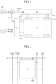
- FIG. 1 is a block diagram illustrating an electroluminescent display device 100 according to an embodiment of the present disclosure.
- the electroluminescent display device 100 includes an image processor 110, a timing controller 120, a gate driver 130, a data driver 140, and a display panel 150.
- the image processor 110 may output image data supplied from the outside and a driving signal for driving various elements.
- the driving signal output from the image processor 110 may include a data enable signal, a vertical sync signal, a horizontal sync signal, and a clock signal.
- the timing controller 120 may be supplied with the image data and the driving signal from the image processor 110.
- the timing controller 120 outputs a gate timing control signal GTC for controlling an operation timing of the gate driver 130 and a data timing control signal DTC for controlling an operation timing of the data driver 140, based on the driving signal.
- the gate driver 130 outputs a scan signal in response to the gate timing control signal GTC supplied from the timing controller 120.
- the gate driver 130 outputs a gate signal through a plurality of gate lines GL1 to GLp (where p is an integer equal to or more than two).
- the gate driver 130 may be implemented as an integrated circuit (IC) type or may be implemented as a gate in panel (GIP) type which is embedded into the display panel 150.
- the gate driver 130 may be disposed on each or one of the left and the right of the display panel 150.
- the gate driver 130 may respectively output first to pth scan signals to first to pth scan lines of the display panel 150.
- the data driver 140 outputs a data voltage in response to the data timing control signal DTC supplied from the timing controller 120.
- the data driver 140 may sample and latch a digital data signal DATA supplied from the timing controller 120 to convert the digital data signal DATA into an analog data signal based on a gamma reference voltage.
- the data driver 140 may output the data signal through a plurality of data lines DL1 to DLq (where q is an integer equal to or more than two).
- the data driver 140 may be provided as an IC type on the display panel 150, or may be provided as a chip on film (COF) type on the display panel 150.
- COF chip on film
- a power supply 180 may output a high-level power voltage VDD, a low-level power voltage VSS, etc.
- the high-level power voltage VDD and the low-level power voltage VSS output from the power supply 180 may be supplied to the display panel 150.
- the high-level power voltage VDD may be supplied to the display panel 150 through a high level power line
- the low-level power voltage VSS may be supplied to the display panel 150 through a low level power line.
- a voltage output from the power supply 180 may be used by the gate driver 130 or the data driver 140.
- the display panel 150 may display an image, based on the gate signal and the data signal respectively supplied from the gate driver 130 and the data driver 140 and a source voltage supplied from the power supply 180.
- the display panel 150 includes a display area, where a plurality of subpixels SP are provided, and a non-display area which is disposed outside the display area and includes various signal lines, a plurality of pads, and/or the like.
- the display area may be an area which displays an image, and thus, may be an area where the subpixels SP are disposed.
- the non-display area may be an area which does not display an image, and thus, may be an area where a plurality of dummy subpixels is disposed or the subpixels SP are not disposed.
- Each subpixel SP may be electrically operated by a pixel circuit.
- the pixel circuit may comprise a first part being arranged in the display area of the display panel 150 and thus may be a part DA of the subpixel SP.
- the pixel circuit may also comprise a second part being arranged in the non-display area DA of the display panel 150 and thus may not be a part of the subpixel SP. The combination of the first part and the second part may form
- the display area may include the plurality of subpixels SP and may display an image, based on a gray level displayed by each of the subpixels SP.
- Each of the subpixels SP may be connected to a data line arranged along a column line and may be connected to a gate line arranged along a pixel line or a row line.
- Subpixels SP connected to the same pixel line may share the same gate line and may be simultaneously supplied with the gate signal through a corresponding gate line. Also, if subpixels SP disposed on a first pixel line are defined as first subpixels and subpixels SP disposed on a pth pixel line are defined as pth subpixels, first to pth subpixels may be sequentially driven.
- the subpixels SP of the display panel 150 may be arranged as a matrix type to configure a pixel array, but are not limited thereto.
- the subpixels SP of the display panel 150 may be arranged as various types such as a pixel sharing type, a stripe type, and a diamond type, in addition to the matrix type.
- the subpixels SP may include a red subpixel, a green subpixel, and a blue subpixel, or may include a white subpixel, a red subpixel, a green subpixel, and a blue subpixel.
- the subpixels SP may have one or more different emission areas, based on an emission characteristic.
- FIG. 2 is a block diagram illustrating a subpixel illustrated in FIG. 1 and signal lines connected to the subpixel SP.
- One subpixel SP may be connected to a gate line GL, a data line DL, a high level power line VDDL, a low level power line VSSL, an initialization voltage line ViniL, and a reference voltage line VrefL.
- the number of transistors and capacitors included in the subpixel SP and a driving method of the subpixel SP may be determined based on a configuration of a pixel circuit, e.g. by the configuration of the first part of the pixel circuit disposed (arranged) on the display area.
- the gate line may include a plurality of scan lines, through which a scan signal is transferred, and a plurality of emission lines through which an emission signal is transferred
- FIG. 3 is a circuit diagram of a subpixel SP according to an illustrative example not forming part of the invention.
- the display panel 150 may include the display area, which displays an image based on the subpixels SP and/or the first part of the pixel circuits, and the non-display DA area which does not display an image and where signal lines, driving circuits, the second part of the pixel circuits, and the like are disposed.
- the electroluminescent display device 100 may display an image based on light emitted from a light emitting device EL included in each of the subpixels SP.
- the voltage drop of a line to which a source voltage is applied occurs due to a sequential shift characteristic where a threshold voltage of an element included in each subpixel SP is shifted and enlarging of the display panel 150, and thus, it is required to compensate for the voltage drop.
- a pixel circuit which recognizes a problem causing an image quality issue such as vertical luminance non-uniformity or crosstalk in an electroluminescent display device an illustrative example not forming part of the invention and solves the problem will be described below. Additionally, the first part of the pixel circuit that is arranged in the display area DA, needs to be miniaturized to enable higher resolutions of the display panel 150.
- An example where a below-described pixel circuit is configured with p-type transistors will be described, but the an illustrative example not forming part of the invention is not limited thereto. In other embodiments, n-type transistors may be applied.
- a subpixel SP according to an illustrative example not forming part of the invention of the present disclosure is a subpixel SP disposed on an nth (where n is a natural number satisfying 1 ⁇ n ⁇ p) pixel line will be described.
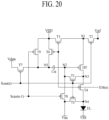
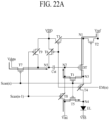
- An nth subpixel SP may include first to seventh transistors T1 to T7, a driving transistor DT, a capacitor Cst, and a light emitting device EL.
- the nth subpixel SP may be implemented based on a total of eight transistors and one capacitor.
- the driving transistor DT may include a source connected to a first node N1, a gate connected to a second node N2, and a drain connected to a third node N3. When a gate-on voltage is applied to the second node N2, the driving transistor DT may be turned on to provide a constant current to the third node N3.
- the first transistor T1 may include a gate connected to an n-lst scan line, a source connected to the second node N2, and a drain connected to the third node N3.
- the first transistor T1 may be turned on in response to a gate-on voltage of an n-lst scan signal Scan(n-1) applied through the n-lst scan line.
- the gate and the drain of the driving transistor DT may be electrically connected to each other, and thus, the driving transistor DT may be in a diode connection state.
- the second transistor T2 may include a gate connected to an nth scan line, a source connected to a reference voltage line, and a drain connected to the first node N1.
- the second transistor T2 may be turned on in response to a gate-on voltage of an nth scan signal Scan(n) applied through the nth scan line.
- a reference voltage Vref may be applied to the first node N1.
- the third transistor T3 may include a gate connected to an nth emission line, a source connected to a high level power line, and a drain connected to the first node N1.
- the third transistor T3 may be turned on in response to a gate-on voltage of an nth emission signal EM(n) applied through the nth emission line.
- a high-level power voltage VDD may be applied to the first node N1.
- the fourth transistor T4 may include a gate connected to an n+1st emission line, a source connected to the third node N3, and a drain connected to a fourth node N4.
- the fourth node N4 may be connected to an anode of the light emitting device EL.
- the fourth transistor T4 may be turned on in response to a gate-on voltage of an n+1st emission signal EM(n+1) applied through the n+1st emission line. When the fourth transistor T4 is turned on, a current may flow between the third node N3 and the fourth node N4.
- the light emitting device EL may include the anode connected to the fourth node N4 and a cathode to which a low-level power voltage VSS is applied.
- a driving current generated through the driving transistor DT may be applied to the anode of the light emitting device EL, and thus, the light emitting device EL may emit light.
- the low-level power voltage VSS may be a voltage of -4V to -2.5V, but is not limited thereto.
- the fifth transistor T5 may include a gate connected to the n-1st scan line, a source connected to the anode of the light emitting device EL, and a drain connected to an initialization line.
- the fifth transistor T5 may be turned on in response to the gate-on voltage of the n-1st scan signal Scan(n-1) applied through the n-1st scan line.
- the anode of the light emitting device EL may be initialized based on an initialization voltage.
- the sixth transistor T6 may include a gate connected to the nth emission line, a source connected to the high level power line, and a drain connected to a fifth node N5.
- the sixth transistor T6 may be turned on in response to the gate-on voltage of the nth emission signal EM(n) applied through the nth emission line.
- the high-level power voltage VDD may be applied to the fifth node N5.
- the capacitor Cst may include a first electrode connected to the second node N2 and a second electrode connected to the fifth node N5.
- the seventh transistor T7 may include a gate connected to the n-lst scan line, a source connected to a data line, and a drain connected to the fifth node N5.
- the seventh transistor T7 may be turned on in response to the gate-on voltage of the n-1st scan signal Scan(n-1) applied through the n-lst scan line.
- a data voltage Vdata may be applied to the fifth node N5.
- a voltage applied to the gate of the driving transistor DT may control a turn-on state of the driving transistor DT, and thus, a transistor including a source or a drain connected to the gate of the driving transistor DT may include two or more transistors serially connected to each other, for maximally suppressing an influence of a leakage current. In this case, the two or more transistors may be controlled by the same control signal. Accordingly, in the nth subpixel SP according to the illustrative example not forming part of the invention, the first transistor T1 may be implemented as a double-gate type transistor.
- the nth subpixel SP may operate in the order of an initialization period, a sampling period, a holding period, a programming period, and an emission period.
- the initialization period may be a period where the gate of the driving transistor DT is initialized
- the sampling period may be a period where a threshold voltage of the driving transistor DT is sampled and a data voltage Vdata is applied through a data line
- the holding period may be a period where the reference voltage Vref is held by a specific node and an error of a voltage applied to the gate of the driving transistor DT in the programming period subsequent thereto is prevented from being caused by an RC delay of the n-1st scan signal Scan(n-1).
- the programming period may be a period where the high-level power voltage VDD is applied to the gate and the source of the driving transistor DT
- the emission period may be a period where the light emitting device EL emits light with a driving current generated based on the data voltage Vdata.
- the nth subpixel SP may have an initialization period INI, a sampling period SAM, a holding period HLD, and a programming period PRG during a period where a gate-off voltage of the nth emission signal EM(n) or the n+1s emission signal EM(n+1) is applied, and thus, compensation based on an internal circuit may be performed.
- An operation characteristic during the periods will be described below.
- a gate-on voltage of a scan signal may be applied during two horizontal periods 2H, and a gate-off voltage of an emission signal may be applied during three horizontal periods 3H.
- each of the initialization period INI, the sampling period SAM, the holding period HLD, and the programming period PRG may be executed during one horizontal period 1H. Driving of the pixel circuit will be described below with reference to the drawings.
- FIG. 4A is a diagram for describing driving of the subpixel according to the illustrative example not forming part of the invention in the initialization period.
- FIG. 4B is a waveform diagram for describing driving of the subpixel illustrated in FIG. 4A .
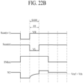
- the n-lst scan signal Scan(n-1) and the n+1st emission signal EM(n+1) may each have a gate-on voltage
- the nth scan signal Scan(n) and the nth emission signal EM(n) may each have a gate-off voltage.
- the gate-on voltage may be a logic low voltage VL and may be -8V
- the gate-off voltage may be a logic high voltage VH and may be 8V.
- the first transistor T1, the fifth transistor T5, and the seventh transistor T7 may be turned on by the gate-on voltage applied through the n-lst scan line, and the fourth transistor T4 may be turned on by the gate-on voltage applied through the n+1st emission line.
- An initialization voltage Vini may be applied to the second node N2 through the turned-on first transistor T1, fourth transistor T4, and fifth transistor T5, and thus, the gate of the driving transistor DT may be initialized to the initialization voltage Vini.
- the data voltage Vdata may be applied to the fifth node T5 through the turned-on transistor T7, thereby preventing changing of the second node N2.
- the initialization voltage Vini may be a voltage which is equal to or lower than the low-level power voltage VSS.
- the initialization voltage Vini may be a voltage of -4V to -3V
- the data voltage Vdata may be a voltage which varies within a range of 0.3V to 6.3V, based on luminance.
- the gate of the driving transistor DT may be initialized based on the initialization voltage Vini, and the capacitor Cst may be charged with the initialization voltage Vini and the data voltage Vdata.
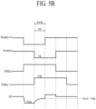
- FIG. 5A is a diagram for describing driving of the subpixel according to the illustrative example not forming part of the invention in the sampling period.
- FIG. 5B is a waveform diagram for describing driving of the subpixel illustrated in FIG. 5A .
- the n-lst scan signal Scan(n-1) and the nth scan signal Scan(n) may each have a gate-on voltage, and the nth emission signal EM(n) and the n+1st emission signal EM(n+1) may each have a gate-off voltage.
- a period where the n-lst scan signal Scan(n-1) has the gate-on voltage and a period where the nth scan signal Scan(n) has the gate-on voltage may overlap each other in the sampling period SAM.
- the first transistor T1, the fifth transistor T5, and the seventh transistor T7 may maintain a turn-on state with the gate-on voltage applied through the n-lst scan line, and the second transistor T2 may be turned on by the gate-on voltage applied through the nth scan line and may be in the diode connection state.
- the reference voltage Vref may be applied to the source of the driving transistor DT through the turned-on second transistor T2, and the gate and the drain of the driving transistor DT may be connected to each other by the turned-on first transistor T1, whereby the driving transistor DT may be turned on.
- a voltage of the second node N2 connected to the gate of the driving transistor DT may increase up to a sum of the reference voltage Vref and a threshold voltage Vth of the driving transistor DT.
- the data voltage Vdata applied to the fifth node N5 in the initialization period INI may be maintained even in the sampling period SAM. Therefore, a voltage corresponding to the sum of the reference voltage Vref and the threshold voltage Vth of the driving transistor DT may be applied to the first electrode of the capacitor Cst, and the data voltage Vdata may be applied to the second electrode of the capacitor Cst, whereby the capacitor Cst may be charged with a difference voltage "Vdata-(Vref+Vth)" between the voltage applied to the first electrode and the data voltage applied to the second electrode. Also, the fifth transistor T5 may be turned on to initialize the anode of the light emitting device EL to the initialization voltage Vini.
- the reference voltage Vref may be a voltage which is higher than the low-level power voltage VSS and is lower than the high-level power voltage VDD.
- the reference voltage Vref may be 4V
- the threshold voltage Vth may be -4V.
- one electrode of the capacitor Cst may be held by applying the data voltage Vdata to the fifth node N5, and by applying the reference voltage Vref to the source of the driving transistor DT, the second node N2 may sample the threshold voltage Vth of the driving transistor DT and may sense the reference voltage Vref.
- FIG. 6A is a diagram for describing driving of the subpixel according to the illustrative example not forming part of the invention in the holding period.
- FIG. 6B is a waveform diagram for describing driving of the subpixel illustrated in FIG. 6A .
- the nth scan signal Scan(n) may have a gate-on voltage
- the n-lst scan signal Scan(n-1), the nth emission signal EM(n), and the n+1st emission signal EM(n+1) may each have a gate-off voltage.
- the second transistor T2 may maintain a turn-on state with the gate-on voltage applied through the nth scan signal Scan(n).
- the reference voltage Vref may be applied to the first node N1 through the turned-on second transistor T2.
- the capacitor Cst may be charged with the data voltage Vdata and may hold the data voltage Vdata, based on a voltage difference between both ends thereof.
- the n-lst scan signal Scan(n-1) may be shifted from the gate-on voltage to the gate-off voltage, and thus, a voltage at the gate of the driving transistor DT may slightly vary due to a parasitic capacitor of the first transistor T1. In this case, the driving transistor DT may be in a turn-off state.
- FIG. 7A is a diagram for describing driving of the subpixel according to the illustrative example not forming part of the invention in the programming period.
- FIG. 7B is a waveform diagram for describing driving of the subpixel illustrated in FIG. 7A .
- the nth emission signal EM(n) may have a gate-on voltage
- the n-1st scan signal Scan(n-1), the nth scan signal Scan(n), and the n+1st emission signal EM(n+1) may each have a gate-off voltage.
- the third transistor T3 and the sixth transistor T6 may be turned on by the gate-on voltage of the nth emission signal EM(n) applied thereto.
- the high-level power voltage VDD may be applied to the first node N1 through the turned-on third transistor T3, and the high-level power voltage VDD may be applied to the fifth node N5 through the turned-on sixth transistor T6.
- a voltage of the fifth node N5 connected to the second electrode of the capacitor Cst may be shifted from the data voltage Vdata to the high-level power voltage VDD, and due to coupling of the capacitor Cst, a voltage at the first electrode of the capacitor Cst may vary by a voltage variation of the fifth node N5.
- a voltage of the second node N2 connected to the first electrode of the capacitor Cst may become "Vref+Vth+(VDD-Vdata)".
- the driving transistor DT since the high-level power voltage VDD is applied to the source of the driving transistor DT, the driving transistor DT may be turned on, but since the fourth transistor T4 is in a turn-off state, the light emitting device EL may not emit light.
- the high-level power voltage VDD may be 4.6V, but is not limited thereto.
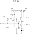
- FIG. 8A is a diagram for describing driving of the subpixel according to the illustrative example not forming part of the invention in the emission period.
- FIG. 8B is a waveform diagram for describing driving of the subpixel illustrated in FIG. 8A .
- the nth emission signal EM(n) and the n+1st emission signal EM(n+1) may each have a gate-on voltage, and the n-lst scan signal Scan(n-1) and the nth scan signal Scan(n) may each have a gate-off voltage.
- the third transistor T3 and the sixth transistor T6 may maintain a turn-on state with the gate-on voltage of the nth emission signal EM(n) applied thereto. Therefore, the second electrode of the capacitor Cst and the source of the driving transistor DT may maintain the high-level power voltage VDD, and thus, the driving transistor DT may maintain a turn-on state. Also, the fourth transistor T4 may be turned on by the gate-on voltage of the n+1st emission signal EM(n+1) applied thereto, and thus, may allow a current to flow between the third node N3 and the fourth node N4.
- a driving current generated in the turned-on driving transistor DT may be applied to the anode of the light emitting device EL through the fourth transistor T4 to allow the light emitting device EL to emit light. Also, by connecting the gate of the fourth transistor T4 to the n+1st emission signal line, the gate of the driving transistor DT may be initialized in the initialization period INI, and the driving current may be applied to the anode of the light emitting device EL in the emission period EMI.
- the high-level power voltage VDD may be reflected in each of the source and the gate of the driving transistor DT through the holding period HLD, in order to consider the voltage drop of the high-level power voltage VDD.
- Ioled denotes a current flowing through the light emitting device EL
- K denotes a constant
- Vgs denotes a voltage between the gate and the source of the driving transistor DT
- Vth denotes the threshold voltage of the driving transistor DT
- VDD denotes the high-level power voltage applied through the high level power line VDDL
- Vref denotes the reference voltage applied through the reference voltage line VrefL
- Vdata denotes a data voltage applied through the data line DL.
- Ioled may be determined based on a difference between the reference voltage and the data voltage.
- the voltage drop of the high-level power voltage is compensated for, based on the high-level power voltage VDD which is applied to the gate and the source of the driving transistor DT in the holding period HLD and the reference voltage Vref which is applied to the source of the driving transistor DT in the sampling period SAM and the holding period HLD.
- a driving circuit for compensating for a sequential shift characteristic based on the voltage drop of the high-level power voltage may be implemented, and thus, an image quality issue such as the vertical luminance non-uniformity or crosstalk of a display device is solved.
- the second and third transistors T2 and T3 of the plurality of transistors configuring the nth subpixel SP may be disposed on one side of the non-display area and may be used in common by q (where q is an integer equal to or more than two) number of subpixels disposed on an nth pixel line.
- the second and third transistors T2 and T3 may be disposed in each of a left non-display area and a right non-display area and may be used in common by q/2 number of subpixels.
- the number of transistors configuring each subpixel is reduced, and thus, each subpixel is efficiently designed, thereby implementing a high-resolution display device.
- the other transistors which are driving transistor DT, first transistor T1, fourth transistor T4, fifth transistor T5, sixth transistor T6, seventh transistor T7 except for the second and third transistors T2 and T3 among the plurality of transistors, the light emitting device EL and the capacitor Cst configuring the nth subpixel SP may be necessary for an individual operation of each subpixel SP are disposed in the display area, and thus, cannot be used in common by the nth pixel line. Accordingly, since the second and third transistors T2 and T3 are disposed in the non-display area DA, the high-resolution display device may be implemented.
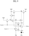
- FIG. 9 is a circuit diagram of a subpixel according to a second illustrative example not forming part of the invention.
- FIG. 9 is a modification example where one transistor is added to the pixel circuit of FIG. 3 , and thus, overlapping descriptions are omitted or will be briefly described.
- An nth subpixel SP may include first to eighth transistors T1 to T8, a driving transistor DT, a capacitor Cst, and a light emitting device EL.
- the nth subpixel SP may be implemented based on a total of nine transistors and one capacitor.
- the driving transistor DT may include a source connected to a first node N1, a gate connected to a second node N2, and a drain connected to a third node N3. When a gate-on voltage is applied to the second node N2, the driving transistor DT may be turned on to provide a constant current to the third node N3.
- the first transistor T1 may include a gate connected to an nth scan line, a source connected to the second node N2, and a drain connected to the third node N3.
- the first transistor T1 may be turned on in response to a gate-on voltage of an nth scan signal Scan(n) applied through the nth scan line.
- the gate and the drain of the driving transistor DT may be electrically connected to each other, and thus, the driving transistor DT may be in a diode connection state.
- the second transistor T2 may include a gate connected to the nth scan line, a source connected to a reference voltage line, and a drain connected to the first node N1.
- the second transistor T2 may be turned on in response to a gate-on voltage of an nth scan signal Scan(n) applied through the nth scan line.
- a reference voltage Vref may be applied to the first node N1.
- the third transistor T3 may include a gate connected to an nth emission line, a source connected to a high level power line, and a drain connected to the first node N1.
- the third transistor T3 may be turned on in response to a gate-on voltage of an nth emission signal EM(n) applied through the nth emission line.
- a high-level power voltage VDD may be applied to the first node N1.
- the fourth transistor T4 may include a gate connected to an nth emission line, a source connected to the third node N3, and a drain connected to a fourth node N4.
- the fourth node N4 may be connected to an anode of the light emitting device EL.
- the fourth transistor T4 may be turned on in response to a gate-on voltage of the nth emission signal EM(n) applied through the nth emission line. When the fourth transistor T4 is turned on, a current may flow between the third node N3 and the fourth node N4.
- the light emitting device EL may include the anode connected to the fourth node N4 and a cathode to which a low-level power voltage VSS is applied.
- a driving current generated through the driving transistor DT may be applied to the anode of the light emitting device EL, and thus, the light emitting device EL may emit light.
- the low-level power voltage VSS may be a voltage of-4V to -2.5V.
- the fifth transistor T5 may include a gate connected to the nth scan line, a source connected to the anode of the light emitting device EL, and a drain connected to an initialization line.
- the fifth transistor T5 may be turned on in response to the gate-on voltage of the nth scan signal Scan(n) applied through the nth scan line.
- the anode of the light emitting device EL may be initialized based on an initialization voltage.
- the sixth transistor T6 may include a gate connected to the nth emission line, a source connected to the high level power line, and a drain connected to a fifth node N5.
- the sixth transistor T6 may be turned on in response to the gate-on voltage of the nth emission signal EM(n) applied through the nth emission line.
- the high-level power voltage VDD may be applied to the fifth node N5.
- the capacitor Cst may include a first electrode connected to the second node N2 and a second electrode connected to the fifth node N5.
- the seventh transistor T7 may include a gate connected to the nth scan line, a source connected to a data line, and a drain connected to the fifth node N5.
- the seventh transistor T7 may be turned on in response to the gate-on voltage of the nth scan signal Scan(n) applied through the nth scan line.
- a data voltage Vdata may be applied to the fifth node N5.
- the eighth transistor T8 may include a gate connected to an n-lst scan line, a source connected to the second node N2, and a drain connected to an initialization line.
- the eighth transistor T8 may be turned on in response to the gate-on voltage of an n-1st scan signal Scan(n-1) applied through the n-1st scan line.
- an initialization voltage Vini may be applied to the second node N2.
- a voltage applied to the gate of the driving transistor DT may control a turn-on state of the driving transistor DT, and thus, a transistor including a source or a drain connected to the gate of the driving transistor DT may include two or more transistors serially connected to each other, for maximally suppressing an influence of a leakage current. In this case, the two or more transistors may be controlled by the same control signal. Accordingly, in the nth subpixel SP according to the second illustrative example not forming part of the invention, the first transistor T1 and the eighth transistor T8 may each be implemented as a double-gate type transistor.
- the nth subpixel SP may operate in the order of an initialization period, a sampling period, a holding period, and an emission period.
- the initialization period may be a period where the gate of the driving transistor DT is initialized
- the sampling period may be a period where a threshold voltage of the driving transistor DT is sampled and a data voltage Vdata is applied through a data line
- the holding period may be a period where the data voltage Vdata is held by a specific node and undesired emission of light caused by a delay of the scan signal is prevented.
- the emission period may be a period where the light emitting device EL emits light with a driving current generated based on the data voltage Vdata.
- the nth subpixel SP may have an initialization period INI and a sampling period SAM during a period where a gate-off voltage of the nth emission signal EM(n) is applied, and thus, compensation based on an internal circuit may be performed.
- An operation characteristic during the periods will be described below.
- a gate-on voltage of the scan signal may be applied during one horizontal periods 1H
- a gate-off voltage of an emission signal may be applied during three horizontal periods 3H.
- each of the initialization period INI, the sampling period SAM, and the holding period HLD may be executed during one horizontal period 1H. Driving of the pixel circuit will be described below with reference to the drawings.
- FIG. 10A is a diagram for describing driving of the subpixel according to the second illustrative example not forming part of the invention in the initialization period.
- FIG. 10B is a waveform diagram for describing driving of the subpixel illustrated in FIG. 10A .
- the n-lst scan signal Scan(n-1) may have a gate-on voltage
- the nth scan signal Scan(n) and the nth emission signal EM(n) may each have a gate-off voltage.
- the gate-on voltage may be a logic low voltage VL and may be - 8V
- the gate-off voltage may be a logic high voltage VH and may be 8V.
- the eighth transistor T8 may be turned on by the gate-on voltage applied through the n-1st scan line.
- An initialization voltage Vini may be applied to the second node N2 through the turned-on eighth transistor T8, and thus, the gate of the driving transistor DT may be initialized to the initialization voltage Vini.
- the initialization voltage Vini may be a voltage which is equal to or lower than the low-level power voltage VSS.
- the initialization voltage Vini may be a voltage of -4V to -3V
- the data voltage Vdata may be a voltage which varies within a range of 0.3V to 6.3V, based on luminance.
- the gate of the driving transistor DT may be initialized based on the initialization voltage Vini.
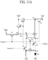
- FIG. 11A is a diagram for describing driving of the subpixel according to the second illustrative example not forming part of the invention in the sampling period.
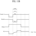
- FIG. 11B is a waveform diagram for describing driving of the subpixel illustrated in FIG. 11A .
- the nth scan signal Scan(n) may have a gate-on voltage
- the n-lst scan signal Scan(n-1) and the nth emission signal EM(n) may each have a gate-off voltage
- the first transistor T1, the second transistor T2, the fifth transistor T5, and the seventh transistor T7 may be turned on by the gate-on voltage applied through the nth scan line.
- the reference voltage Vref may be applied to the source of the driving transistor DT through the turned-on second transistor T2, and the gate and the drain of the driving transistor DT may be connected to each other by the turned-on first transistor T1, whereby the driving transistor DT may be turned on and may be in the diode connection state.
- a voltage of the second node N2 connected to the gate of the driving transistor DT may increase up to a sum of the reference voltage Vref and a threshold voltage Vth of the driving transistor DT.
- the data voltage Vdata may be applied to the fifth node N5 through the turned-on seventh transistor T7.
- a voltage corresponding to the sum of the reference voltage Vref and the threshold voltage Vth of the driving transistor DT may be applied to the first electrode of the capacitor Cst, and the data voltage Vdata may be applied to the second electrode of the capacitor Cst, whereby the capacitor Cst may be charged with a difference voltage "Vdata-(Vref+Vth)" between the voltage applied to the first electrode and the data voltage applied to the second electrode.
- the fifth transistor T5 may be turned on to initialize the anode of the light emitting device EL to the initialization voltage Vini.
- the reference voltage Vref may be a voltage which is higher than the low-level power voltage VSS and is lower than the high-level power voltage VDD.
- the reference voltage Vref may be 4V
- the threshold voltage Vth may be -4V.
- one electrode of the capacitor Cst may be held by applying the data voltage Vdata to the fifth node N5, and by applying the reference voltage Vref to the source of the driving transistor DT, the second node N2 may sample the threshold voltage Vth of the driving transistor DT and may sense the reference voltage Vref.
- FIG. 12A is a diagram for describing driving of the subpixel according to the second illustrative example not forming part of the invention in the holding period.
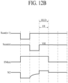
- FIG. 12B is a waveform diagram for describing driving of the subpixel illustrated in FIG. 12A .
- the n-lst scan signal Scan(n-1), the nth scan signal Scan(n), and the nth emission signal EM(n) may each have a gate-on voltage, and thus, the first to eighth transistors T1 to T8 may be turned off.
- the nth scan signal Scan(n) may be shifted from the gate-on voltage to the gate-off voltage, and thus, a voltage at the gate of the driving transistor DT may slightly vary due to a parasitic capacitor of the first transistor T1. In this case, the driving transistor DT may be in a turn-off state.
- the subpixel according to the second illustrative example not forming part of the invention may include the holding period HLD, thereby preventing undesired emission of light caused by a delay of a scan signal.
- FIG. 13A is a diagram for describing driving of the subpixel according to the second illustrative example not forming part of the invention in the emission period.
- FIG. 13B is a waveform diagram for describing driving of the subpixel illustrated in FIG. 13A .
- the nth emission signal EM(n) may have a gate-on voltage.
- the third transistor T3, the fourth transistor T4, and the sixth transistor T6 may be turned on by the gate-on voltage of the nth emission signal EM(n) applied thereto. Therefore, the high-level power voltage VDD may be applied to the second electrode of the capacitor Cst, and thus, due to coupling of the capacitor Cst, a voltage of the second node N2 may become "Vref+Vth+(Vdd-Vdata)". Also, the high-level power voltage VDD may be applied to the source of the driving transistor DT, and thus, the driving transistor DT may be turned on. Also, the fourth transistor T4 may be turned on, and thus, may allow a current to flow between the third node N3 and the fourth node N4. Accordingly, a driving current generated in the turned-on driving transistor DT may be applied to the anode of the light emitting device EL through the fourth transistor T4 to allow the light emitting device EL to emit light.
- Ioled denotes a current flowing through the light emitting device EL
- K denotes a constant
- Vgs denotes a voltage between the gate and the source of the driving transistor DT
- Vth denotes the threshold voltage of the driving transistor DT
- VDD denotes the high-level power voltage applied through the high level power line VDDL
- Vref denotes the reference voltage applied through the reference voltage line VrefL
- Vdata denotes a data voltage applied through the data line DL.
- the high-level power voltage VDD may be 4.6V.
- Ioled may be determined based on a difference between the reference voltage and the data voltage.
- the voltage drop of the high-level power voltage is compensated for, based on the reference voltage Vref which is applied to the source of the driving transistor DT in the sampling period SAM and the high-level power voltage VDD which is applied to the gate and the source of the driving transistor DT in the emission period EMI.
- a driving circuit for compensating for a sequential shift characteristic based on the voltage drop of the high-level power voltage may be implemented, and thus, an image quality issue such as the vertical luminance non-uniformity or crosstalk of a display device is solved.
- the gate of the driving transistor DT may be initialized without adding the n+1st emission signal EM(n+1), and thus, a size of an emission driver for providing an emission signal is reduced, thereby decreasing a size of a bezel which is a non-display area of an electroluminescent display device.
- the second and third transistors T2 and T3 of the plurality of transistors configuring the nth subpixel SP according to the second illustrative example not forming part of the invention may be disposed on one side of the non-display area and may be used in common by q number of subpixels disposed on an nth pixel line.
- the second and third transistors T2 and T3 may be disposed in each of a left non-display area and a right non-display area and may be used in common by q/2 number of subpixels.
- the number of transistors configuring each subpixel is reduced, and thus, each subpixel is efficiently designed, thereby implementing a high-resolution display device.
- the other transistors which are driving transistor DT, first transistor T1, fourth transistor T4, fifth transistor T5, sixth transistor T6, seventh transistor T7, the eight transistor T8 except for the second and third transistors T2 and T3 among the plurality of transistors, the light emitting device EL and the capacitor Cst configuring the nth subpixel SP may be necessary for an individual operation of each subpixel SP are disposed in the display area, and thus, cannot be used in common by the nth pixel line. Accordingly, since the second and third transistors T2 and T3 are disposed in the non-display area, the high-resolution display device may be implemented.
- FIG. 14 is a circuit diagram of a subpixel according to a third illustrative example not forming part of the invention.
- an eighth transistor T8 is added to the subpixel of FIG. 14 , and the fourth transistor T4 illustrated in FIG. 3 is not applied to the subpixel of FIG. 14.
- FIG. 14 is a modification example which is implemented by modifying the pixel circuit of FIG. 3 , and thus, overlapping descriptions are omitted or will be briefly described.
- An nth subpixel SP may include first to third transistors T1 to T3, fifth to seventh transistors T5 to T7, a ninth transistor T9, a driving transistor DT, a capacitor Cst, and a light emitting device EL.
- the nth subpixel SP may be implemented based on a total of eight transistors and one capacitor.
- the driving transistor DT may include a source connected to a first node N1, a gate connected to a second node N2, and a drain connected to a third node N3. When a gate-on voltage is applied to the second node N2, the driving transistor DT may be turned on to provide a constant current to the third node N3.
- the first transistor T1 may include a gate connected to an n+1st scan line, a source connected to the second node N2, and a drain connected to the third node N3.
- the first transistor T1 may be turned on in response to a gate-on voltage of an n+1st scan signal Scan(n+1) applied through the n+1st scan line.
- the gate and the drain of the driving transistor DT may be electrically connected to each other, and thus, the driving transistor DT may be in a diode connection state.
- the second transistor T2 may include a gate connected to an nth scan line, a source connected to a reference voltage line, and a drain connected to the first node N1.
- the second transistor T2 may be turned on in response to a gate-on voltage of an nth scan signal Scan(n) applied through the nth scan line.
- a reference voltage Vref may be applied to the first node N1.
- the third transistor T3 may include a gate connected to an nth emission line, a source connected to a high level power line, and a drain connected to the first node N1.
- the third transistor T3 may be turned on in response to a gate-on voltage of an nth emission signal EM(n) applied through the nth emission line.
- a high-level power voltage VDD may be applied to the first node N1.
- the fifth transistor T5 may include a gate connected to an n-lst scan line, a source connected to a fourth node N4, and a drain connected to an initialization line.
- the fifth transistor T5 may be turned on in response to the gate-on voltage of the n-lst scan signal Scan(n-1) applied through an n-lst scan line.
- the anode of the light emitting device EL may be initialized based on an initialization voltage.
- the fourth node N4 may be the same node as the third node N3.
- the light emitting device EL may include the anode connected to the fourth node N4 and a cathode to which a low-level power voltage VSS is applied.
- VSS low-level power voltage
- the light emitting device EL may emit light.
- the low-level power voltage VSS may be a voltage of -4V to -2.5V.
- the sixth transistor T6 may include a gate connected to the nth emission line, a source connected to the high level power line, and a drain connected to a fifth node N5.
- the sixth transistor T6 may be turned on in response to the gate-on voltage of the nth emission signal EM(n) applied through the nth emission line.
- the high-level power voltage VDD may be applied to the fifth node N5.
- the capacitor Cst may include a first electrode connected to the second node N2 and a second electrode connected to the fifth node N5.
- the ninth transistor T9 may include a gate connected to the n-1st scan line, a source connected to the high level power line, and a drain connected to the fifth node N5.
- the ninth transistor T9 may be turned on in response to the gate-on voltage of the n-lst scan signal Scan(n-1) applied through the n-lst scan line.
- a high-level power voltage VDD may be applied to the fifth node N5.
- the seventh transistor T7 may include a gate connected to the n+1st scan line, a source connected to a data line, and a drain connected to the fifth node N5.
- the seventh transistor T7 may be turned on in response to the gate-on voltage of the n+1st scan signal Scan(n+1) applied through the n+1st scan line.
- a data voltage Vdata may be applied to the fifth node N5.
- a voltage applied to the gate of the driving transistor DT may control a turn-on state of the driving transistor DT, and thus, a transistor including a source or a drain connected to the gate of the driving transistor DT may include two or more transistors serially connected to each other, for maximally suppressing an influence of a leakage current. In this case, the two or more transistors may be controlled by the same control signal. Accordingly, in the nth subpixel SP according to the third illustrative example not forming part of the invention, the first transistor T1 may be implemented as a double-gate type transistor.
- the nth subpixel SP may operate in the order of an initialization period, a first holding period, a sampling period, a second holding period, and an emission period.
- the initialization period may be a period where the anode of the light emitting device EL is initialized
- the first holding period may be a period where a reference voltage Vref is applied to the source of the driving transistor DT
- the sampling period may be a period where the data voltage Vdata is applied to a specific node and a threshold voltage of the driving transistor DT is sampled.
- the second holding period may be a period where the data voltage Vdata is held by the specific node
- the emission period may be a period where the light emitting device EL emits light with a driving current generated based on the data voltage Vdata.
- the nth subpixel SP may have an initialization period INI, a first holding period HLD1, a sampling period SAM, and a second holding period HLD2 during a period where a gate-off voltage of the nth emission signal EM(n) is applied, and thus, compensation based on an internal circuit may be performed.
- An operation characteristic during the periods will be described below.
- a gate-on voltage of a scan signal may be applied during two horizontal periods 2H
- a gate-off voltage of an emission signal may be applied during four horizontal periods 4H.
- each of the initialization period INI, the first holding period HLD1, the sampling period SAM, and the second holding period HLD2 may be executed during one horizontal period 1H. Driving of the pixel circuit will be described below with reference to the drawings.
- FIG. 15A is a diagram for describing driving of the subpixel according to the third illustrative example not forming part of the invention in the initialization period.
- FIG. 15B is a waveform diagram for describing driving of the subpixel illustrated in FIG. 15A .
- the n-lst scan signal Scan(n-1) may have a gate-on voltage
- the nth scan signal Scan(n), the n+1st scan signal Scan(n+1), and the nth emission signal EM(n) may each have a gate-off voltage.
- the gate-on voltage may be a logic low voltage VL and may be -8V
- the gate-off voltage may be a logic high voltage VH and may be 8V.
- the fifth transistor T5 and the ninth transistor T9 may be turned on by the gate-on voltage applied through the n-lst scan line.
- An initialization voltage Vini may be applied to the fourth node N4 through the turned-on fifth transistor T5, and thus, the anode of the light emitting device EL may be initialized to the initialization voltage Vini.
- the initialization voltage Vini may be a voltage which is equal to or lower than the low-level power voltage VSS.
- the initialization voltage Vini may be a voltage of -4V to -3V
- the data voltage Vdata may be a voltage which varies within a range of 0.3V to 6.3V, based on luminance.
- the anode of the light emitting device EL may be initialized based on the initialization voltage Vini, and the high-level power voltage VDD may be applied to one electrode of the capacitor Cst.
- FIG. 16A is a diagram for describing driving of the subpixel according to the third illustrative example not forming part of the invention in the first holding period.
- FIG. 16B is a waveform diagram for describing driving of the subpixel illustrated in FIG. 16A .
- the n-1st scan signal Scan(n-1) and the nth scan signal Scan(n) may each have a gate-on voltage
- the n+1st scan signal Scan(n+1) and the nth emission signal EM(n) may each have a gate-off voltage.
- a period where the n-lst scan signal Scan(n-1) has the gate-on voltage and a period where the nth scan signal Scan(n) has the gate-on voltage may overlap each other in the first holding period HLD1.
- the fifth transistor T5 and the ninth transistor T9 may maintain a turn-on state with the gate-on voltage applied through the n-1st scan line, and the second transistor T2 may be turned on by the gate-on voltage applied through the nth scan line.
- the initialization voltage Vini applied to the anode of the light emitting device EL through the turned-on fifth transistor T5 may be held, the high-level power voltage VDD applied to the fifth node N5 through the turned-on ninth transistor T9 may be held, and the reference voltage Vref may be applied to the first node N1 through the turned-on second transistor T2.
- FIG. 17A is a diagram for describing driving of the subpixel according to the third illustrative example not forming part of the invention in the sampling period.
- FIG. 17B is a waveform diagram for describing driving of the subpixel illustrated in FIG. 17A .
- the nth scan signal Scan(n) and the n+1st scan signal Scan(n+1) may each have a gate-on voltage
- the n-1st scan signal Scan(n-1) and the nth emission signal EM(n) may each have a gate-off voltage
- the second transistor T2 may maintain a turn-on state with the gate-on voltage applied through the nth scan line, and the first transistor T1 may be turned on by the gate-on voltage applied through the n+1st scan line, whereby the driving transistor DT may be in the diode connection state.
- the reference voltage Vref applied through the turned-on second transistor T2 may be held by the source of the driving transistor DT, and the gate and the drain of the driving transistor DT may be connected to each other by the turned-on first transistor T1, whereby the driving transistor DT may be turned on.
- a voltage of the second node N2 connected to the gate of the driving transistor DT may increase up to a sum of the reference voltage Vref and a threshold voltage Vth of the driving transistor DT.
- the data voltage Vdata may be applied to the fifth node N5 by the seventh transistor T7 which is turned on by the gate-on voltage applied through the n+1st scan line. Therefore, a voltage corresponding to the sum of the reference voltage Vref and the threshold voltage Vth of the driving transistor DT may be applied to the first electrode of the capacitor Cst, and the data voltage Vdata may be applied to the second electrode of the capacitor Cst, whereby the capacitor Cst may be charged with a difference voltage "Vdata-(Vref+Vth)" between the voltage applied to the first electrode and the data voltage applied to the second electrode.
- the reference voltage Vref may be a voltage which is higher than the low-level power voltage VSS and is lower than the high-level power voltage VDD.
- the reference voltage Vref may be 4V
- the threshold voltage Vth may be -4V.
- one electrode of the capacitor Cst may be held by applying the data voltage Vdata to the fifth node N5, and by applying the reference voltage Vref to the source of the driving transistor DT, the second node N2 may sample the threshold voltage Vth of the driving transistor DT and may sense the reference voltage Vref.
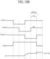
- FIG. 18A is a diagram for describing driving of the subpixel according to the third illustrative example not forming part of the invention in the second holding period.
- FIG. 18B is a waveform diagram for describing driving of the subpixel illustrated in FIG. 18A .
- the n+1st scan signal Scan(n+1) may hold a gate-on voltage
- the n-lst scan signal Scan(n-1), the nth scan signal Scan(n), and the nth emission signal EM(n) may each have a gate-off voltage.
- the first transistor T1 and the seventh transistor T7 may maintain a turn-on state with the gate-on voltage applied through the n+1st scan signal Scan(n+1).
- the capacitor Cst may be charged with the data voltage Vdata and may hold the data voltage Vdata, based on a voltage difference between both ends thereof.
- FIG. 19A is a diagram for describing driving of the subpixel according to the third illustrative example not forming part of the invention in the emission period.
- FIG. 19B is a waveform diagram for describing driving of the subpixel illustrated in FIG. 19A .
- the nth emission signal EM(n) may have a gate-on voltage
- the n-lst scan signal Scan(n-1), the nth scan signal Scan(n), and the n+1st scan signal Scan(n+1) may each have a gate-off voltage
- the third transistor T3 and the sixth transistor T6 may be turned on by the gate-on voltage of the nth emission signal EM(n) applied thereto.
- the high-level power voltage VDD may be applied to the first node N1 through the turned-on third transistor T3, and the high-level power voltage VDD may be applied to the fifth node N5 through the turned-on sixth transistor T6.
- a voltage of the fifth node N5 connected to the second electrode of the capacitor Cst may be shifted from the data voltage Vdata to the high-level power voltage VDD, and due to coupling of the capacitor Cst, a voltage at the first electrode of the capacitor Cst may vary by a voltage variation of the fifth node N5.
- a voltage of the second node N2 connected to the first electrode of the capacitor Cst may become "Vref+Vth+(VDD-Vdata)".
- the driving transistor DT since the high-level power voltage VDD is applied to the source of the driving transistor DT, the driving transistor DT may be turned on to apply a driving current to the anode of the light emitting device EL. Therefore, the light emitting device EL may emit light.
- the high-level power voltage VDD may be 4.6V.
- the high-level power voltage VDD may be applied to each of the source and the gate of the driving transistor DT, in order to consider the voltage drop of the high-level power voltage VDD.
- Ioled denotes a current flowing through the light emitting device EL
- K denotes a constant
- Vgs denotes a voltage between the gate and the source of the driving transistor DT
- Vth denotes the threshold voltage of the driving transistor DT
- VDD denotes the high-level power voltage applied through the high level power line VDDL
- Vref denotes the reference voltage applied through the reference voltage line VrefL
- Vdata denotes a data voltage applied through the data line DL.
- Ioled may be determined based on a difference between the reference voltage and the data voltage.
- the voltage drop of the high-level power voltage is compensated for, based on the high-level power voltage VDD which is applied to the gate and the source of the driving transistor DT in the emission period EMI and the reference voltage Vref which is applied to the source of the driving transistor DT in the sampling period SAM.
- a driving circuit for compensating for a sequential shift characteristic based on the voltage drop of the high-level power voltage may be implemented, and thus, an image quality issue such as the vertical luminance non-uniformity or crosstalk of a display device is solved.
- the second and third transistors T2 and T3 of the plurality of transistors configuring the nth subpixel SP may be disposed on one side of the non-display area and may be used in common by q number of subpixels disposed on an nth pixel line.
- the second and third transistors T2 and T3 may be disposed in each of a left non-display area and a right non-display area and may be used in common by q/2 number of subpixels.
- the number of transistors configuring each subpixel is reduced, and thus, each subpixel is efficiently designed, thereby implementing a high-resolution display device.
- the other transistors which are driving transistor DT, first transistor T1, the fifth transistor T5, sixth transistor T6, seventh transistor T7, the ninth transistor T9 except for the second and third transistors T2 and T3 among the plurality of transistors, the light emitting device EL and the capacitor Cst configuring the nth subpixel SP may be necessary for an individual operation of each subpixel SP are disposed in the display area, and thus, cannot be used in common by the nth pixel line. Accordingly, since the second and third transistors T2 and T3 are disposed in the non-display area, the high-resolution display device may be implemented.
- FIG. 20 is a circuit diagram of a subpixel according to a embodiment of the present disclosure.
- FIG. 20 is a modification example where two transistors are added to the pixel circuit of FIG. 3 , and thus, overlapping descriptions are omitted or will be briefly described.
- An nth subpixel SP includes first to ninth transistors T1 to T9, a driving transistor DT, a capacitor Cst, and a light emitting device EL.
- the nth subpixel SP may be implemented based on a total of ten transistors and one capacitor.
- the driving transistor DT may include a source connected to a first node N1, a gate connected to a second node N2, and a drain connected to a third node N3. When a gate-on voltage is applied to the second node N2, the driving transistor DT may be turned on to provide a constant current to the third node N3.
- the first transistor T1 may include a gate connected to an nth scan line, a source connected to the second node N2, and a drain connected to the third node N3.
- the first transistor T1 may be turned on in response to a gate-on voltage of an nth scan signal Scan(n) applied through the nth scan line.
- the gate and the drain of the driving transistor DT may be electrically connected to each other, and thus, the driving transistor DT may be in a diode connection state.
- the second transistor T2 may include a gate connected to the nth scan line, a source connected to a reference voltage line, and a drain connected to the first node N1.
- the second transistor T2 is turned on in response to a gate-on voltage of an nth scan signal Scan(n) applied through the nth scan line.
- a reference voltage Vref is applied to the first node N1.
- the third transistor T3 may include a gate connected to an nth emission line, a source connected to a high level power line, and a drain connected to the first node N1.
- the third transistor T3 is turned on in response to a gate-on voltage of an nth emission signal EM(n) applied through the nth emission line.
- EM(n) an nth emission signal
- VDD a high-level power voltage
- the fourth transistor T4 may include a gate connected to an nth emission line, a source connected to the third node N3, and a drain connected to a fourth node N4.
- the fourth node N4 may be connected to an anode of the light emitting device EL.
- the fourth transistor T4 is turned on in response to a gate-on voltage of the nth emission signal EM(n) applied through the nth emission line. When the fourth transistor T4 is turned on, a current flows between the third node N3 and the fourth node N4.
- the fifth transistor T5 may include a gate connected to the nth scan line, a source connected to the fourth node N4, and a drain connected to an initialization line.
- the fifth transistor T5 is turned on in response to the gate-on voltage of the nth scan signal Scan(n) applied through the nth scan line.
- an initialization voltage Vini is applied to the fourth node N4, and thus, the anode of the light emitting device EL may be initialized.
- the sixth transistor T6 may include a gate connected to the nth emission line, a source connected to the high level power line, and a drain connected to a fifth node N5.
- the sixth transistor T6 is turned on in response to the gate-on voltage of the nth emission signal EM(n) applied through the nth emission line.
- the ninth transistor T9 may include a gate connected to the n-1st scan line, a source connected to the high level power line, and a drain connected to the fifth node N5.
- the ninth transistor T9 is turned on in response to the gate-on voltage of the n-lst scan signal Scan(n-1) applied through the n-lst scan line.
- a high-level power voltage VDD is applied to the fifth node N5.
- the capacitor Cst includes a first electrode connected to the second node N2 and a second electrode connected to the fifth node N5.
- the seventh transistor T7 may include a gate connected to the nth scan line, a source connected to a data line, and a drain connected to the fifth node N5.
- the seventh transistor T7 is turned on in response to the gate-on voltage of the nth scan signal Scan(n) applied through the nth scan line.
- a data voltage Vdata is applied to the fifth node N5.
- the eighth transistor T8 may include a gate connected to an n-lst scan line, a source connected to the second node N2, and a drain connected to an initialization line.
- the eighth transistor T8 is turned on in response to the gate-on voltage of an n-1st scan signal Scan(n-1) applied through the n-1st scan line.
- an initialization voltage Vini is applied to the second node N2.
- the light emitting device EL includes the anode connected to the fourth node N4 and a cathode to which a low-level power voltage VSS is applied.
- a driving current generated through the driving transistor DT may be applied to the anode of the light emitting device EL, and thus, the light emitting device EL may emit light.
- the low-level power voltage VSS may be a voltage of-4V to -2.5V, but is not limited thereto.
- a voltage applied to the gate of the driving transistor DT may control a turn-on state of the driving transistor DT, and thus, a transistor including a source or a drain connected to the gate of the driving transistor DT may include two or more transistors serially connected to each other, for maximally suppressing an influence of a leakage current. In this case, the two or more transistors may be controlled by the same control signal. Accordingly, in the nth subpixel SP according to the embodiment of the present disclosure, the first transistor T1 and the eighth transistor T8 may each be implemented as a double-gate type transistor.
- the nth subpixel SP operates in the order of an initialization period, a sampling period, a holding period, and an emission period.
- the initialization period may be a period where the gate of the driving transistor DT is initialized
- the sampling period may be a period where a threshold voltage of the driving transistor DT is sampled and a data voltage Vdata is applied through a data line
- the holding period may be a period where undesired emission of light caused by a delay of the scan signal is prevented.
- the emission period may be a period where the light emitting device EL emits light with a driving current generated based on the data voltage Vdata.
- the nth subpixel SP have an initialization period INI and a sampling period SAM during a period where a gate-off voltage of the nth emission signal EM(n) is applied, and thus, compensation based on an internal circuit may be performed.
- An operation characteristic during the periods will be described below.
- a gate-on voltage of the scan signal may be applied during one horizontal periods 1H
- a gate-off voltage of an emission signal may be applied during three horizontal periods 3H.
- each of the initialization period INI, the sampling period SAM, and the holding period HLD may be executed during one horizontal period 1H. Driving of the pixel circuit will be described below with reference to the drawings.
- FIG. 21A is a diagram for describing driving of the subpixel according to the embodiment of the present disclosure in the initialization period.
- FIG. 21B is a waveform diagram for describing driving of the subpixel illustrated in FIG. 21A .
- the n-lst scan signal Scan(n-1) has a gate-on voltage
- the nth scan signal Scan(n) and the nth emission signal EM(n) each have a gate-off voltage.
- the gate-on voltage may be a logic low voltage VL and may be - 8V
- the gate-off voltage may be a logic high voltage VH and may be 8V.
- the present embodiment is not limited thereto.
- the ninth transistor T9 and the eighth transistor T8 are turned on by the gate-on voltage applied through the n-lst scan line.
- the high-level power voltage VDD may be applied to the fifth node N5 through the turned-on ninth transistor T9, and an initialization voltage Vini may be applied to the second node N2 through the turned-on eighth transistor T8, whereby the gate of the driving transistor DT may be initialized to the initialization voltage Vini.
- the initialization voltage Vini may be a voltage which is equal to or lower than the low-level power voltage VSS.
- the initialization voltage Vini may be a voltage of -4V to -3V
- the data voltage Vdata may be a voltage which varies within a range of 0.3V to 6.3V, based on luminance.
- the gate of the driving transistor DT may be initialized based on the initialization voltage Vini.
- FIG. 22A is a diagram for describing driving of the subpixel according to the embodiment of the present disclosure in the sampling period.
- FIG. 22B is a waveform diagram for describing driving of the subpixel illustrated in FIG. 22A .
- the nth scan signal Scan(n) have a gate-on voltage
- the n-lst scan signal Scan(n-1) and the nth emission signal EM(n) each have a gate-off voltage.
- the first transistor T1, the second transistor T2, the fifth transistor T5, and the seventh transistor T7 are turned on by the gate-on voltage applied through the nth scan line.
- the reference voltage Vref may be applied to the source of the driving transistor DT through the turned-on second transistor T2, and the gate and the drain of the driving transistor DT may be connected to each other by the turned-on first transistor T1, whereby the driving transistor DT may be turned on and may be in the diode connection state.
- a voltage of the second node N2 connected to the gate of the driving transistor DT may increase up to a sum of the reference voltage Vref and a threshold voltage Vth of the driving transistor DT.
- the data voltage Vdata may be applied to the fifth node N5 through the turned-on seventh transistor T7.
- a voltage corresponding to the sum of the reference voltage Vref and the threshold voltage Vth of the driving transistor DT may be applied to the first electrode of the capacitor Cst, and the data voltage Vdata may be applied to the second electrode of the capacitor Cst, whereby the capacitor Cst may be charged with a difference voltage "Vdata-(Vref+Vth)" between the voltage applied to the first electrode and the data voltage applied to the second electrode.
- the fifth transistor T5 may be turned on to initialize the anode of the light emitting device EL to the initialization voltage Vini.
- the reference voltage Vref may be 4V
- the threshold voltage Vth may be -4V.
- the present embodiment is not limited thereto.
- one electrode of the capacitor Cst may be held by applying the data voltage Vdata to the fifth node N5, and by applying the reference voltage Vref to the source of the driving transistor DT, the second node N2 may sample the threshold voltage Vth of the driving transistor DT and may sense the reference voltage Vref.
- FIG. 23A is a diagram for describing driving of the subpixel according to the embodiment of the present disclosure in the holding period.
- FIG. 23B is a waveform diagram for describing driving of the subpixel illustrated in FIG. 23A .
- the n-lst scan signal Scan(n-1), the nth scan signal Scan(n), and the nth emission signal EM(n) each have a gate-on voltage, and thus, the first to ninth transistors T1 to T9 are turned off.
- the nth scan signal Scan(n) are shifted from the gate-on voltage to the gate-off voltage, and thus, a voltage at the gate of the driving transistor DT may slightly vary due to a parasitic capacitor of the first transistor T1. In this case, the driving transistor DT may be in a turn-off state.
- the subpixel according to the embodiment of the present disclosure may include the holding period HLD, thereby preventing undesired emission of light caused by a delay of a scan signal.
- FIG. 24A is a diagram for describing driving of the subpixel according to the embodiment of the present disclosure in the emission period.
- FIG. 24B is a waveform diagram for describing driving of the subpixel illustrated in FIG. 24A .
- the nth emission signal EM(n) has a gate-on voltage.
- the third transistor T3, the sixth transistor T6, and the fourth transistor T4 are turned on by the gate-on voltage of the nth emission signal EM(n) applied thereto. Therefore, the high-level power voltage VDD may be applied to the second electrode of the capacitor Cst, and thus, due to coupling of the capacitor Cst, a voltage of the second node N2 may become "Vref+Vth+(Vdd-Vdata)". Also, the high-level power voltage VDD may be applied to the source of the driving transistor DT, and thus, the driving transistor DT may be turned on. Also, the fourth transistor T4 may be turned on, and thus, may allow a current to flow between the third node N3 and the fourth node N4.
- a driving current generated in the turned-on driving transistor DT may be applied to the anode of the light emitting device EL through the fourth transistor T4 to allow the light emitting device EL to emit light.
- the fourth transistor T5 may maintain a turn-off state in a period other than the emission period EMI, thereby preventing undesired emission of light.
- Ioled denotes a current flowing through the light emitting device EL
- K denotes a constant
- Vgs denotes a voltage between the gate and the source of the driving transistor DT
- Vth denotes the threshold voltage of the driving transistor DT
- VDD denotes the high-level power voltage applied through the high level power line VDDL
- Vref denotes the reference voltage applied through the reference voltage line VrefL
- Vdata denotes a data voltage applied through the data line DL.
- the high-level power voltage VDD may be 4.6V.
- Ioled may be determined based on a difference between the reference voltage and the data voltage.
- the voltage drop of the high-level power voltage is compensated for, based on the reference voltage Vref which is applied to the source of the driving transistor DT in the sampling period SAM and the high-level power voltage VDD which is applied to the gate and the source of the driving transistor DT in the emission period EMI.
- a driving circuit for compensating for a sequential shift characteristic based on the voltage drop of the high-level power voltage may be implemented, and thus, an image quality issue such as the vertical luminance non-uniformity or crosstalk of a display device is solved
- the gate of the driving transistor DT may be initialized, thereby preventing an increase in luminance of a black screen of the display panel.
- the second and third transistors T2 and T3 of the plurality of transistors configuring the nth subpixel SP may be disposed on one side of the non-display area and may be used in common by q number of subpixels disposed on an nth pixel line.
- the second and third transistors T2 and T3 may be disposed in each of a left non-display area and a right non-display area and may be used in common by q/2 number of subpixels. Therefore, the number of transistors configuring each subpixel is reduced, and thus, each subpixel is efficiently designed, thereby implementing a high-resolution display device.
- the other transistors which are driving transistor DT, first transistor T1, fourth transistor T4, fifth transistor T5, sixth transistor T6, seventh transistor T7, the eight transistor T8, the ninth transistor T9 except for the second and third transistors T2 and T3 among the plurality of transistors, the light emitting device EL and the capacitor Cst configuring the nth subpixel SP may be necessary for an individual operation of each subpixel, and thus, cannot be used in common by the nth pixel line. Accordingly, since the second and third transistors T2 and T3 are disposed in the non-display area, the high-resolution display device may be implemented.
- the electroluminescent display device according to embodiments of the present disclosure will be described as follows.
- the electroluminescent display device includes a display panel including a plurality of pixel lines each including a plurality of pixel circuits. Also, each of the plurality of pixel circuits included in an nth (where n is a natural number) pixel line of the plurality of pixel lines includes a driving transistor connected between a first node and a third node and including a gate connected to a second node, a first transistor allowing a current to flow between the second node and the third node in response to an n-1st scan signal, a second transistor applying a reference voltage to the first node in response to an nth scan signal, a third transistor applying a high-level power voltage to the first node in response to an nth emission signal, a fourth transistor allowing a current to flow between the third node and a fourth node in response to an n+1st emission signal, a fifth transistor applying an initialization voltage to the fourth node in response to
- the display panel may include a display area and a non-display area. Accordingly, a subpixel supplied with the reference voltage may provide the light emitting device with a driving current unaffected by the high-level power voltage, thereby solving an image quality issue of the electroluminescent display device.
- the reference voltage may be a voltage which is higher than the low-level power voltage and is lower than the high-level power voltage
- the initialization voltage may be a voltage which is equal to or lower than the low-level power voltage
- a period where the n-1st scan signal has a gate-on voltage and a period where the nth scan signal has the gate-on voltage may overlap each other.
- the n-1st scan signal and the nth scan signal may be activated to the gate-on voltage during two horizontal periods, and the nth emission signal and the n+1st emission signal may be deactivated to a gate-off voltage during three horizontal periods.
- one frame for driving each of the plurality of pixel circuits may include an initialization period where a gate-on voltage of the n-1st scan signal is input to an n-1st pixel line and the gate-on voltage of the n+1st emission signal is held by an n+1st pixel line, a sampling period where the gate-on voltage of the n-1st scan signal is held by the n-1st pixel line and the gate-on voltage of the nth scan signal is input to an nth pixel line, a holding period where the gate-on voltage of the nth scan signal is held by the nth pixel line, a programming period where the gate-on voltage of the nth emission signal is input to the nth pixel line, and an emission period where the light emitting device emits light.
- the first transistor, the fourth transistor, the fifth transistor, and the seventh transistor may be turned on, and in the sampling period, the first transistor, the second transistor, the fifth transistor, and the seventh transistor may be turned on. Also, in the holding period, the second transistor may be turned on, and in the programming period, the third transistor and the sixth transistor may be turned on. Also, in the emission period, the third transistor, the fourth transistor, and the sixth transistor may be turned on.
- the first transistor may be a double-gate type transistor.
- the electroluminescent display device includes a display panel including a plurality of pixel lines each including a plurality of pixel circuits. Also, each of the plurality of pixel circuits included in an nth pixel line of the plurality of pixel lines includes a driving transistor connected between a first node and a third node and including a gate connected to a second node, a first transistor allowing a current to flow between the second node and the third node in response to an nth scan signal, a second transistor applying a reference voltage to the first node in response to the nth scan signal, a third transistor applying a high-level power voltage to the first node in response to an nth emission signal, a fourth transistor allowing a current to flow between the third node and a fourth node in response to the nth emission signal, a fifth transistor applying an initialization voltage to the fourth node in response to the nth scan signal, a sixth transistor applying the high
- the display panel may include a display area and a non-display area. Accordingly, a subpixel supplied with the reference voltage may provide the light emitting device with a driving current unaffected by the high-level power voltage, thereby solving an image quality issue of the electroluminescent display device.
- one frame for driving each of the plurality of pixel circuits may include an initialization period where a gate-on voltage of the n-1st scan signal is input to an n-1st pixel line, a sampling period where the gate-on voltage of the nth scan signal is input to an nth pixel line, a holding period where a gate-off voltage of each of the n-1st scan signal and the nth scan signal is input to the nth pixel line, and an emission period where the gate-on voltage of the nth emission signal is input to the nth pixel line.
- the eighth transistor may be turned on, and in the sampling period, the first transistor, the second transistor, the fifth transistor, and the seventh transistor may be turned on. Also, in the holding period, the first to eighth transistors may be turned off, and in the emission period, the third transistor, the fourth transistor, and the sixth transistor may be turned on.
- the nth emission signal in the initialization period, the sampling period, and the holding period, may have the gate-off voltage.
- the n-1st scan signal and the nth scan signal may be activated to the gate-on voltage during one horizontal period, and the nth emission signal may be deactivated to the gate-off voltage during three horizontal periods.
- each of the first transistor and the eighth transistor may be a double-gate type transistor.
- the electroluminescent display device includes a display panel including a plurality of pixel lines each including a plurality of pixel circuits. Also, each of the plurality of pixel circuits included in an nth pixel line of the plurality of pixel lines includes a driving transistor connected between a first node and a third node and including a gate connected to a second node, a first transistor allowing a current to flow between the second node and the third node in response to an n+1st scan signal, a second transistor applying a reference voltage to the first node in response to an nth scan signal, a third transistor applying a high-level power voltage to the first node in response to an nth emission signal, a fifth transistor applying an initialization voltage to the fourth node in response to an n-1st scan signal, a sixth transistor applying the high-level power voltage to a fifth node in response to the nth emission signal, a ninth transistor applying the high-
- the display panel may include a display area and a non-display area. Accordingly, a subpixel supplied with the reference voltage may provide the light emitting device with a driving current unaffected by the high-level power voltage, thereby solving an image quality issue of the electroluminescent display device.
- the reference voltage may be a voltage which is higher than the low-level power voltage and is lower than the high-level power voltage
- the initialization voltage may be a voltage which is equal to or lower than the low-level power voltage
- a period where the n-1st scan signal has a gate-on voltage and a period where the nth scan signal has the gate-on voltage may overlap each other.
- the n-1st scan signal and the nth scan signal may be activated to the gate-on voltage during two horizontal periods, and the nth emission signal may be deactivated to a gate-off voltage during four horizontal periods.
- one frame for driving each of the plurality of pixel circuits may include an initialization period where a gate-on voltage of the n-1st scan signal is input to an n-lst pixel line, a first holding period where the gate-on voltage of the n-1st scan signal is held by the n-lst pixel line and the gate-on voltage of the nth scan signal is input to an nth pixel line, a sampling period where the gate-on voltage of the nth scan signal is held by the nth pixel line and the gate-on voltage of the n+1st scan signal is input to an n+1st pixel line, a second holding period where the gate-on voltage of the n+1st scan signal is held by the n+1st pixel line, and an emission period where the light emitting device emits light.
- the fifth transistor and the ninth transistor may be turned on, and in the first holding period, the second transistor, the fifth transistor, and the ninth transistor may be turned on.
- the first transistor, the second transistor, and the seventh transistor may be turned on, and in the second holding period, the first transistor and the seventh may be turned on.
- the third transistor and the sixth transistor may be turned on.
- the first transistor may be a double-gate type transistor.
- the electroluminescent display device includes a display panel including a plurality of pixel lines each including a plurality of pixel circuits. Also, each of the plurality of pixel circuits included in an nth pixel line of the plurality of pixel lines includes a driving transistor connected between a first node and a third node and including a gate connected to a second node, a first transistor allowing a current to flow between the second node and the third node in response to an nth scan signal, a second transistor applying a reference voltage to the first node in response to the nth scan signal, a third transistor applying a high-level power voltage to the first node in response to an nth emission signal, a fifth transistor applying an initialization voltage to a fourth node in response to the nth scan signal, a sixth transistor applying the high-level power voltage to a fifth node in response to the nth emission signal, a ninth transistor applying the high-level power voltage
- the display panel may include a display area and a non-display area. Accordingly, a subpixel supplied with the reference voltage may provide the light emitting device with a driving current unaffected by the high-level power voltage, thereby solving an image quality issue of the electroluminescent display device.
- one frame for driving each of the plurality of pixel circuits may include an initialization period where a gate-on voltage of the n-1st scan signal is input to an n-1st pixel line, a sampling period where the gate-on voltage of the nth scan signal is input to an nth pixel line, a holding period where a gate-off voltage of each of the n-1st scan signal and the nth scan signal is input to the nth pixel line, and an emission period where the gate-on voltage of the nth emission signal is input to the nth pixel line.
- the ninth transistor and the eighth transistor may be turned on, and in the sampling period, the first transistor, the second transistor, the fifth transistor, and the seventh transistor may be turned on. Also, in the holding period, the first to ninth transistors may be turned off, and in the emission period, the third transistor, the sixth transistor, and the fourth transistor may be turned on.
- the nth emission signal in the initialization period, the sampling period, and the holding period, may have the gate-off voltage.
- the n-1st scan signal and the nth scan signal may be activated to the gate-on voltage during one horizontal period, and the nth emission signal may be deactivated to the gate-off voltage during three horizontal periods.
- each of the first transistor and the eighth transistor may be a double-gate type transistor.
- the second transistor and the third transistor may be in the non-display area.
- the second transistor and the third transistor may be used in common by each the plurality of pixel lines.
- the initialization voltage may be equal to or lower than the low-level power voltage
- the reference voltage may be higher than the low-level power voltage and lower than the high-level power voltage
- a pixel circuit for compensating for a sequential shift characteristic based on the voltage drop of a source voltage may be implemented, thereby solving an image quality issue such as the vertical luminance non-uniformity or cross-talk of a display panel.
- some of a plurality of transistors for driving each pixel circuit may be disposed in a non-display area and may be used in common by pixel circuits connected to the same pixel line, and thus, an efficiency of designing pixel circuits is enhanced, thereby realizing a high-resolution display device.
Landscapes
- Engineering & Computer Science (AREA)
- Physics & Mathematics (AREA)
- Computer Hardware Design (AREA)
- General Physics & Mathematics (AREA)
- Theoretical Computer Science (AREA)
- Microelectronics & Electronic Packaging (AREA)
- Control Of Indicators Other Than Cathode Ray Tubes (AREA)
- Control Of El Displays (AREA)
- Electroluminescent Light Sources (AREA)
Claims (7)
- Elektrolumineszenz-Anzeigevorrichtung, die Folgendes umfasst:einen Bildprozessor (110);eine Zeitvorgabesteuereinheit (120), die mit Bilddaten und Ansteuerungssignalen von dem Bildprozessor (110) versorgt wird und konfiguriert ist, ein Gate-Zeitvorgabesteuersignal (GTC-Signal) zum Steuern einer Betriebszeitvorgabe eines Gate-Treibers (130) und ein Daten-Zeitvorgabesteuersignal (DTC-Signal) zum Steuern einer Betriebszeitvorgabe eines Daten-Treibers (140) auszugeben;den Gate-Treiber (130), der konfiguriert ist, in Reaktion auf das Gate-Zeitvorgabesteuersignal (GTC-Signal) Abtastsignale auszugeben und über mehrere Gate-Leitungen (GL1 bis GLp) ein Gate-Signal auszugeben, wobei die Gate-Leitungen (GL1 bis GLp) Abtastleitungen, über die Abtastsignale übertragen werden, und Emissionsleitungen, über die Emissionssignale übertragen werden, umfassen;den Daten-Treiber (140), der konfiguriert ist, in Reaktion auf das Daten-Zeitvorgabesteuersignal (DTC-Signal) eine Datenspannung auszugeben und Datensignale über mehrere Datenleitungen (DL1 bis DLq) auszugeben; undeine Anzeigetafel (150), die einen Anzeigebereich und einen Nichtanzeigebereich aufweist,wobei die Anzeigetafel (150) mehrere Pixel-Leitungen enthält, wovon jede mehrere Pixel-Schaltungen enthält,wobei jede der mehreren Pixel-Schaltungen, die in einer n-ten Pixel-Leitung (wobei n eine natürliche Zahl ist) der mehreren Pixel-Leitungen enthalten ist, Folgendes umfasst:eine erste Abtastleitung;eine zweite Abtastleitung;eine Emissionsleitung;einen Ansteuerungstransistor (DT), der zwischen einen ersten Knoten (N1) und einen dritten Knoten (N3) geschaltet ist und ein Gate, das mit einem zweiten Knoten (N2) verbunden ist, aufweist;einen ersten Transistor (T1), der zwischen den zweiten Knoten (N2) und den dritten Knoten (N3) geschaltet ist und ein Gate aufweist, das mit der ersten Abtastleitung verbunden ist, um zuzulassen, dass in Reaktion auf ein n-tes Abtastsignal (Scan(n)), das an die erste Abtastleitung angelegt wird, ein Strom zwischen dem zweiten Knoten (N2) und dem dritten Knoten (N3) fließt;einen zweiten Transistor (T2), der zwischen den ersten Knoten (N1) und eine Referenzspannungsquelle (Vref) geschaltet ist und ein Gate aufweist, das mit der ersten Abtastleitung verbunden ist und in Reaktion auf das n-te Abtastsignal (Scan(n)), das an die erste Abtastleitung angelegt wird, die Referenzspannung (Vref) an den ersten Knoten (N1) angelegt;einen dritten Transistor (T3), der zwischen den ersten Knoten (N1) und eine Leistungsspannungsquelle (VDD) mit hohem Pegel geschaltet ist und einen Gate aufweist, das mit der Emissionsleitung verbunden ist und in Reaktion auf ein n-tes Emissionssignal (EM(n)), das an die Emissionsleitung angelegt wird, die Leistungsspannung (VDD) mit hohem Pegel an den ersten Knoten (N1) angelegt;einen vierten Transistor (T4), der zwischen den dritten Knoten (N3) und einen vierten Knoten (N4) geschaltet ist und ein Gate aufweist, das mit der Emissionsleitung verbunden ist, um zuzulassen, dass in Reaktion auf ein n-tes Emissionssignal (EM(n)), das an die Emissionsleitung angelegt wird, zwischen dem dritten Knoten (N3) und dem vierten Knoten (N4) ein Strom fließt;einen fünften Transistor (T5), der zwischen den vierten Knoten (N4) und eine Initialisierungsspannungsquelle (Vini) geschaltet ist und ein Gate aufweist, das mit der ersten Abtastschaltung verbunden ist und in Reaktion auf das n-te Abtastsignal (Scan(n)), das an die erste Abtastleitung angelegt wird, die Initialisierungsspannung (Vini) an den vierten Knoten (N4) anlegt;einen sechsten Transistor (T6), der zwischen einen fünften Knoten (N5) und die Leistungsspannungsquelle (VDD) mit hohem Pegel geschaltet ist und ein Gate aufweist, das mit der Emissionsleitung verbunden ist und in Reaktion auf das n-te Emissionssignal (EM(n)), das an die Emissionsleitung angelegt wird, die Leistungsspannung (VDD) mit hohem Pegel an den fünften Knoten (N5) anlegt;einen siebten Transistor (T7), der zwischen den fünften Knoten (N5) und eine Datenleitung geschaltet ist und ein Gate aufweist, das mit der ersten Abtastleitung verbunden ist und in Reaktion auf das n-te Abtastsignal (Scan(n)), das an die erste Abtastleitung angelegt wird, eine Datenspannung an den fünften Knoten (N5) anlegt;einen achten Transistor (T8), der zwischen den zweiten Knoten (N2) und die Initialisierungsstrahlungsquelle (Vini) geschaltet ist und ein Gate aufweist, das mit der zweiten Abtastleitung verbunden ist und in Reaktion auf ein (n - 1)-tes Abtastsignal (Scan(n - 1)), das an die zweite Abtastleitung angelegt wird, dem zweiten Knoten (N2) die Initialisierungsspannung (Vini) zuführt;einen neunten Transistor (T9), der zwischen den fünften Knoten (N5) und die Leistungsspannungsquelle (VDD) mit hohem Pegel geschaltet ist und ein Gate aufweist, das mit der zweiten Abtastleitung verbunden ist und in Reaktion auf das (n - 1)-te Abtastsignal (Scan(n - 1)), das an die zweite Abtastleitung angelegt wird, die Leistungsspannung mit hohem Pegel an den fünften Knoten (N5) anlegt;einen Kondensator (Cst), der zwischen den zweiten Knoten (N2) und den fünften Knoten (N5) geschaltet ist; undeine Lichtemissionsvorrichtung (EL), die eine Anode, die mit dem vierten Knoten (N4) verbunden ist, und eine Katode, die mit einer Leitung verbunden ist, an die eine Leistungsspannung (VSS) mit niedrigem Pegel angelegt wird, aufweist;wobei der Gate-Treiber dafür ausgelegt ist, die Abtastsignale und die Emissionssignale auszugeben, derart, dassein Rahmen zum Ansteuern jeder der mehreren Pixel-Schaltungen Folgendes enthält:eine Initialisierungsperiode, in der eine Gate-Durchschaltspannung des (n - 1)-ten Abtastsignals (Scan(n - 1)) in die erste Abtastleitung der Pixel, die einer (n - 1)-ten Pixel-Leitung entsprechen, und in die zweite Abtastleitung der Pixel, die einer n-ten Pixel-Leitung entsprechen, eingegeben wird,eine Abtastperiode, die der Initialisierungsperiode folgt und in der die Gate-Durchschaltspannung des n-ten Abtastsignals (Scan(n)) in die erste Abtastleitung der Pixel, die der n-ten Pixel-Leitung entsprechen, eingegeben wird,eine Halteperiode, die der Abtastperiode entspricht und in der eine Gate-Sperrspannung sowohl des (n - 1)-ten Abtastsignals (Scan(n - 1)) als auch des n-ten Abtastsignals (Scan(n)) in die zweite Abtastleitung bzw. in die erste Abtastleitung der Pixel, die der n-ten Pixel-Leitung entsprechen, eingegeben werden,eine Emissionsperiode, die der Halteperiode folgt und in der die Gate-Durchschaltspannung des n-ten Emissionssignals (EM(n)) in die Emissionsleitung der Pixel, die der n-ten Pixel-Leitung entsprechen, eingegeben wird,wobei in der Initialisierungsperiode, der Abtastperiode und der Halteperiode das n-te Emissionssignal (EM(n)) die Gate-Sperrspannung besitzt,in der Initialisierungsperiode der neunte Transistor (T9) und der achte Transistor (T8) durchgeschaltet sind,in der Abtastperiode der erste Transistor (T1), der zweite Transistor (T2), der fünfte Transistor (T5) und der siebte Transistor (T7) durchgeschaltet sind,in der Halteperiode die ersten bis neunten Transistoren (T1, T2, T3, T4, T5, T6, T7, T8, T9) gesperrt sind undin der Emissionsperiode der dritte Transistor (T3), der sechste Transistor (T6) und der vierte Transistor (T4) durchgeschaltet sind.
- Elektrolumineszenz-Anzeigevorrichtung nach Anspruch 1, wobei sowohl der erste Transistor als auch der achte Transistor ein Transistor des Typs mit doppeltem Gate sind.
- Elektrolumineszenz-Anzeigevorrichtung nach einem der vorhergehenden Ansprüche, wobei der zweite Transistor (T2) und/oder der dritte Transistor (T3) in dem Nichtanzeigebereich angeordnet sind.
- Elektrolumineszenz-Anzeigevorrichtung nach Anspruch 3, wobei der zweite Transistor (T2) und der dritte Transistor (T3) von jeder der mehreren Pixel-Leitungen gemeinsam verwendet werden.
- Elektrolumineszenz-Anzeigevorrichtung nach einem der vorhergehenden Ansprüche, wobei die Initialisierungsspannung (Vini) gleich oder niedriger als die Leistungsspannung (VSS) mit niedrigem Pegel ist.
- Elektrolumineszenz-Anzeigevorrichtung nach einem der vorhergehenden Ansprüche, wobei die Referenzspannung (Vref) höher als die Leistungsspannung (VSS) mit niedrigem Pegel und niedriger als die Leistungsspannung (VDD) mit hohem Pegel ist.
- Elektrolumineszenz-Anzeigevorrichtung nach einem der vorhergehenden Ansprüche, wobei der Ansteuerungstransistor (DT), der erste Transistor (T1), der vierte Transistor (T4), der fünfte Transistor (T5), der sechste Transistor (T6), der siebte Transistor (T7), der achte Transistor (T8), die Lichtemissionsvorrichtung (EL) und der Kondensator (Cst) in dem Anzeigebereich angeordnet sind.
Applications Claiming Priority (2)
| Application Number | Priority Date | Filing Date | Title |
|---|---|---|---|
| KR1020170163682A KR20190064265A (ko) | 2017-11-30 | 2017-11-30 | 전계발광 표시장치 |
| KR1020170163688A KR102439226B1 (ko) | 2017-11-30 | 2017-11-30 | 전계발광 표시장치 |
Publications (2)
| Publication Number | Publication Date |
|---|---|
| EP3493189A1 EP3493189A1 (de) | 2019-06-05 |
| EP3493189B1 true EP3493189B1 (de) | 2023-08-30 |
Family
ID=62904331
Family Applications (1)
| Application Number | Title | Priority Date | Filing Date |
|---|---|---|---|
| EP18182401.2A Active EP3493189B1 (de) | 2017-11-30 | 2018-07-09 | Elektrolumineszente anzeigevorrichtung |
Country Status (2)
| Country | Link |
|---|---|
| US (2) | US10438538B2 (de) |
| EP (1) | EP3493189B1 (de) |
Families Citing this family (31)
| Publication number | Priority date | Publication date | Assignee | Title |
|---|---|---|---|---|
| CN109192140B (zh) * | 2018-09-27 | 2020-11-24 | 武汉华星光电半导体显示技术有限公司 | 像素驱动电路和显示装置 |
| KR102693495B1 (ko) * | 2018-10-08 | 2024-08-12 | 삼성디스플레이 주식회사 | 표시 장치 |
| KR102631739B1 (ko) | 2018-11-29 | 2024-01-30 | 엘지디스플레이 주식회사 | 서브화소 구동 회로 및 이를 포함한 전계발광 표시장치 |
| CN112424856B (zh) * | 2019-06-03 | 2023-03-14 | 京东方科技集团股份有限公司 | 像素电路、像素电路的驱动方法、显示装置及其驱动方法 |
| CN110060652A (zh) * | 2019-06-10 | 2019-07-26 | 北海惠科光电技术有限公司 | 阵列基板、显示装置及其驱动方法 |
| TWI713011B (zh) * | 2019-08-27 | 2020-12-11 | 友達光電股份有限公司 | 畫素電路 |
| WO2021053459A1 (ja) * | 2019-09-20 | 2021-03-25 | 株式会社半導体エネルギー研究所 | 表示装置、表示モジュール、及び電子機器 |
| KR102686613B1 (ko) * | 2020-02-24 | 2024-07-22 | 삼성디스플레이 주식회사 | 유기발광 디스플레이 장치 및 이의 구동 방법 장치 및 이를 포함하는 디스플레이 시스템 |
| KR102772693B1 (ko) * | 2020-06-02 | 2025-02-26 | 삼성디스플레이 주식회사 | 유기 발광 표시 장치의 화소, 및 유기 발광 표시 장치 |
| KR102764939B1 (ko) * | 2020-07-09 | 2025-02-12 | 삼성디스플레이 주식회사 | 표시 장치 |
| CN114333686A (zh) * | 2020-09-25 | 2022-04-12 | 京东方科技集团股份有限公司 | 驱动电路和显示面板 |
| CN112102778B (zh) * | 2020-10-10 | 2022-12-06 | 京东方科技集团股份有限公司 | 像素电路及其驱动方法、显示基板和显示装置 |
| KR102836199B1 (ko) * | 2020-11-30 | 2025-07-17 | 엘지디스플레이 주식회사 | 전계발광 표시장치 |
| KR102878047B1 (ko) * | 2020-12-31 | 2025-10-30 | 엘지디스플레이 주식회사 | 표시 장치 및 그의 구동 방법 |
| KR102867650B1 (ko) * | 2021-06-30 | 2025-10-14 | 윤구(구안) 테크놀로지 컴퍼니 리미티드 | 픽셀 구동 회로 및 그 구동 방법과 디스플레이 패널 |
| WO2023274230A1 (zh) * | 2021-06-30 | 2023-01-05 | 云谷(固安)科技有限公司 | 像素电路、显示面板 |
| CN113539174A (zh) * | 2021-07-12 | 2021-10-22 | 京东方科技集团股份有限公司 | 像素电路及其驱动方法、显示装置 |
| DE112021008261T5 (de) * | 2021-09-23 | 2024-08-22 | Boe Technology Group Co., Ltd. | Anzeigepanel und anzeigegerät |
| KR102913143B1 (ko) * | 2021-11-03 | 2026-01-19 | 삼성디스플레이 주식회사 | 화소 및 이를 포함하는 표시 장치 |
| KR20230073405A (ko) * | 2021-11-18 | 2023-05-26 | 삼성디스플레이 주식회사 | 표시 장치 |
| KR102824387B1 (ko) * | 2021-11-22 | 2025-06-26 | 삼성디스플레이 주식회사 | 표시 장치 및 이의 구동 방법 |
| CN114120881A (zh) | 2021-12-13 | 2022-03-01 | 武汉华星光电半导体显示技术有限公司 | 像素电路、显示装置及其驱动方法 |
| KR20230110412A (ko) | 2022-01-14 | 2023-07-24 | 삼성디스플레이 주식회사 | 화소 및 이를 포함하는 표시 장치 |
| CN117581288A (zh) | 2022-05-19 | 2024-02-20 | 京东方科技集团股份有限公司 | 驱动模组、显示面板和显示装置 |
| KR20230168631A (ko) * | 2022-06-07 | 2023-12-15 | 삼성디스플레이 주식회사 | 표시 장치 |
| KR20240128758A (ko) * | 2023-02-17 | 2024-08-27 | 삼성디스플레이 주식회사 | 표시 패널 및 이를 포함하는 표시 장치 |
| US20240388277A1 (en) * | 2023-05-17 | 2024-11-21 | Innolux Corporation | Electronic circuit |
| CN120356418A (zh) * | 2024-01-22 | 2025-07-22 | 群创光电股份有限公司 | 电子电路 |
| KR20250132238A (ko) * | 2024-02-28 | 2025-09-04 | 엘지디스플레이 주식회사 | 투명 디스플레이 장치 |
| CN121359191A (zh) * | 2024-05-16 | 2026-01-16 | 京东方科技集团股份有限公司 | 显示基板及其驱动方法、显示装置 |
| CN118711534A (zh) * | 2024-07-30 | 2024-09-27 | 京东方科技集团股份有限公司 | 像素驱动电路、驱动方法及显示面板 |
Family Cites Families (14)
| Publication number | Priority date | Publication date | Assignee | Title |
|---|---|---|---|---|
| JP2009271200A (ja) * | 2008-05-01 | 2009-11-19 | Sony Corp | 表示装置及びその駆動方法 |
| KR101097325B1 (ko) * | 2009-12-31 | 2011-12-23 | 삼성모바일디스플레이주식회사 | 화소 회로 및 유기 전계 발광 표시 장치 |
| KR101859474B1 (ko) * | 2011-09-05 | 2018-05-23 | 엘지디스플레이 주식회사 | 유기 발광 다이오드 표시 장치의 화소 회로 |
| KR101985243B1 (ko) * | 2012-09-26 | 2019-06-05 | 엘지디스플레이 주식회사 | 유기전계발광표시장치, 이의 구동방법 및 이의 제조방법 |
| CN103021333B (zh) * | 2012-12-11 | 2016-01-20 | 昆山工研院新型平板显示技术中心有限公司 | 有机发光显示器的像素电路及其驱动方法 |
| KR102307500B1 (ko) * | 2015-03-20 | 2021-10-01 | 삼성디스플레이 주식회사 | 표시 장치의 화소회로 및 이를 포함하는 표시 장치 |
| KR102559083B1 (ko) * | 2015-05-28 | 2023-07-25 | 엘지디스플레이 주식회사 | 유기발광 표시장치 |
| EP3098804A3 (de) * | 2015-05-28 | 2016-12-21 | LG Display Co., Ltd. | Organische lichtemittierende anzeige |
| KR102503160B1 (ko) * | 2015-09-30 | 2023-02-24 | 엘지디스플레이 주식회사 | 유기발광다이오드 표시장치 |
| KR102546774B1 (ko) * | 2016-07-22 | 2023-06-23 | 삼성디스플레이 주식회사 | 표시 장치 및 그 구동 방법 |
| KR102633522B1 (ko) * | 2016-10-25 | 2024-02-07 | 엘지디스플레이 주식회사 | 유기발광표시장치 및 그 구동장치 |
| KR102573334B1 (ko) * | 2016-12-28 | 2023-09-01 | 엘지디스플레이 주식회사 | 유기발광표시장치 및 그의 구동방법 |
| CN107274829B (zh) * | 2017-07-10 | 2020-04-14 | 上海天马有机发光显示技术有限公司 | 一种有机电致发光显示面板及显示设备 |
| US10872570B2 (en) * | 2017-08-31 | 2020-12-22 | Lg Display Co., Ltd. | Electroluminescent display device for minimizing a voltage drop and improving image quality and driving method thereof |
-
2018
- 2018-07-09 EP EP18182401.2A patent/EP3493189B1/de active Active
- 2018-07-18 US US16/038,460 patent/US10438538B2/en active Active
-
2019
- 2019-09-06 US US16/563,803 patent/US10540928B2/en active Active
Also Published As
| Publication number | Publication date |
|---|---|
| US10540928B2 (en) | 2020-01-21 |
| US10438538B2 (en) | 2019-10-08 |
| US20190392764A1 (en) | 2019-12-26 |
| EP3493189A1 (de) | 2019-06-05 |
| US20190164491A1 (en) | 2019-05-30 |
Similar Documents
| Publication | Publication Date | Title |
|---|---|---|
| EP3493189B1 (de) | Elektrolumineszente anzeigevorrichtung | |
| KR102926045B1 (ko) | 서브화소 구동 회로 및 이를 포함한 전계발광 표시장치 | |
| EP3451321B1 (de) | Elektrolumineszente anzeigevorrichtung und ansteuerungsverfahren dafür | |
| KR102650560B1 (ko) | 전계 발광 표시장치 | |
| KR20240040703A (ko) | 전계 발광 표시장치 | |
| US9837023B2 (en) | Color display device with pixel circuits including two capacitors | |
| KR20210073188A (ko) | 화소 구동 회로를 포함한 전계발광 표시장치 | |
| JP2021529333A (ja) | 駆動回路及びその駆動方法、表示装置 | |
| KR20200135524A (ko) | 픽셀 구동 회로 및 그 구동 방법, 및 디스플레이 패널 | |
| KR20200013923A (ko) | 게이트 구동부 및 이를 이용한 전계발광 표시장치 | |
| KR20210075435A (ko) | 화소 구동 회로를 포함한 전계발광 표시장치 | |
| US20120105427A1 (en) | Display device | |
| KR20190064265A (ko) | 전계발광 표시장치 | |
| CN116386506B (zh) | 包括像素驱动电路的显示设备 | |
| KR102439226B1 (ko) | 전계발광 표시장치 | |
| CN116403532A (zh) | 栅极驱动电路及使用该栅极驱动电路的电致发光显示装置 | |
| KR20250131065A (ko) | 픽셀 회로 및 이를 포함하는 표시장치 | |
| KR102658432B1 (ko) | 발광 제어 신호 발생부 및 이를 포함하는 발광 표시 장치 | |
| KR102570977B1 (ko) | 전계발광 표시장치 및 이의 구동방법 | |
| KR20240170614A (ko) | 표시 장치 | |
| KR102696836B1 (ko) | 발광 제어 신호 발생부 및 이를 포함하는 발광 표시 장치 | |
| KR20230086084A (ko) | 표시 장치 | |
| KR20240086084A (ko) | 디스플레이 장치 및 게이트 구동 회로 | |
| KR20250125104A (ko) | 표시 장치 | |
| KR20250112479A (ko) | 픽셀 회로와 이를 포함한 표시장치 |
Legal Events
| Date | Code | Title | Description |
|---|---|---|---|
| PUAI | Public reference made under article 153(3) epc to a published international application that has entered the european phase |
Free format text: ORIGINAL CODE: 0009012 |
|
| STAA | Information on the status of an ep patent application or granted ep patent |
Free format text: STATUS: REQUEST FOR EXAMINATION WAS MADE |
|
| 17P | Request for examination filed |
Effective date: 20180709 |
|
| AK | Designated contracting states |
Kind code of ref document: A1 Designated state(s): AL AT BE BG CH CY CZ DE DK EE ES FI FR GB GR HR HU IE IS IT LI LT LU LV MC MK MT NL NO PL PT RO RS SE SI SK SM TR |
|
| AX | Request for extension of the european patent |
Extension state: BA ME |
|
| RBV | Designated contracting states (corrected) |
Designated state(s): AL AT BE BG CH CY CZ DE DK EE ES FI FR GB GR HR HU IE IS IT LI LT LU LV MC MK MT NL NO PL PT RO RS SE SI SK SM TR |
|
| STAA | Information on the status of an ep patent application or granted ep patent |
Free format text: STATUS: EXAMINATION IS IN PROGRESS |
|
| 17Q | First examination report despatched |
Effective date: 20200925 |
|
| GRAP | Despatch of communication of intention to grant a patent |
Free format text: ORIGINAL CODE: EPIDOSNIGR1 |
|
| STAA | Information on the status of an ep patent application or granted ep patent |
Free format text: STATUS: GRANT OF PATENT IS INTENDED |
|
| INTG | Intention to grant announced |
Effective date: 20230314 |
|
| GRAS | Grant fee paid |
Free format text: ORIGINAL CODE: EPIDOSNIGR3 |
|
| GRAA | (expected) grant |
Free format text: ORIGINAL CODE: 0009210 |
|
| STAA | Information on the status of an ep patent application or granted ep patent |
Free format text: STATUS: THE PATENT HAS BEEN GRANTED |
|
| AK | Designated contracting states |
Kind code of ref document: B1 Designated state(s): AL AT BE BG CH CY CZ DE DK EE ES FI FR GB GR HR HU IE IS IT LI LT LU LV MC MK MT NL NO PL PT RO RS SE SI SK SM TR |
|
| REG | Reference to a national code |
Ref country code: GB Ref legal event code: FG4D |
|
| REG | Reference to a national code |
Ref country code: CH Ref legal event code: EP |
|
| REG | Reference to a national code |
Ref country code: DE Ref legal event code: R096 Ref document number: 602018056298 Country of ref document: DE |
|
| REG | Reference to a national code |
Ref country code: IE Ref legal event code: FG4D |
|
| REG | Reference to a national code |
Ref country code: LT Ref legal event code: MG9D |
|
| REG | Reference to a national code |
Ref country code: NL Ref legal event code: MP Effective date: 20230830 |
|
| REG | Reference to a national code |
Ref country code: AT Ref legal event code: MK05 Ref document number: 1606465 Country of ref document: AT Kind code of ref document: T Effective date: 20230830 |
|
| PG25 | Lapsed in a contracting state [announced via postgrant information from national office to epo] |
Ref country code: GR Free format text: LAPSE BECAUSE OF FAILURE TO SUBMIT A TRANSLATION OF THE DESCRIPTION OR TO PAY THE FEE WITHIN THE PRESCRIBED TIME-LIMIT Effective date: 20231201 |
|
| PG25 | Lapsed in a contracting state [announced via postgrant information from national office to epo] |
Ref country code: IS Free format text: LAPSE BECAUSE OF FAILURE TO SUBMIT A TRANSLATION OF THE DESCRIPTION OR TO PAY THE FEE WITHIN THE PRESCRIBED TIME-LIMIT Effective date: 20231230 |
|
| PG25 | Lapsed in a contracting state [announced via postgrant information from national office to epo] |
Ref country code: SE Free format text: LAPSE BECAUSE OF FAILURE TO SUBMIT A TRANSLATION OF THE DESCRIPTION OR TO PAY THE FEE WITHIN THE PRESCRIBED TIME-LIMIT Effective date: 20230830 Ref country code: RS Free format text: LAPSE BECAUSE OF FAILURE TO SUBMIT A TRANSLATION OF THE DESCRIPTION OR TO PAY THE FEE WITHIN THE PRESCRIBED TIME-LIMIT Effective date: 20230830 Ref country code: NO Free format text: LAPSE BECAUSE OF FAILURE TO SUBMIT A TRANSLATION OF THE DESCRIPTION OR TO PAY THE FEE WITHIN THE PRESCRIBED TIME-LIMIT Effective date: 20231130 Ref country code: LV Free format text: LAPSE BECAUSE OF FAILURE TO SUBMIT A TRANSLATION OF THE DESCRIPTION OR TO PAY THE FEE WITHIN THE PRESCRIBED TIME-LIMIT Effective date: 20230830 Ref country code: LT Free format text: LAPSE BECAUSE OF FAILURE TO SUBMIT A TRANSLATION OF THE DESCRIPTION OR TO PAY THE FEE WITHIN THE PRESCRIBED TIME-LIMIT Effective date: 20230830 Ref country code: IS Free format text: LAPSE BECAUSE OF FAILURE TO SUBMIT A TRANSLATION OF THE DESCRIPTION OR TO PAY THE FEE WITHIN THE PRESCRIBED TIME-LIMIT Effective date: 20231230 Ref country code: HR Free format text: LAPSE BECAUSE OF FAILURE TO SUBMIT A TRANSLATION OF THE DESCRIPTION OR TO PAY THE FEE WITHIN THE PRESCRIBED TIME-LIMIT Effective date: 20230830 Ref country code: GR Free format text: LAPSE BECAUSE OF FAILURE TO SUBMIT A TRANSLATION OF THE DESCRIPTION OR TO PAY THE FEE WITHIN THE PRESCRIBED TIME-LIMIT Effective date: 20231201 Ref country code: FI Free format text: LAPSE BECAUSE OF FAILURE TO SUBMIT A TRANSLATION OF THE DESCRIPTION OR TO PAY THE FEE WITHIN THE PRESCRIBED TIME-LIMIT Effective date: 20230830 Ref country code: AT Free format text: LAPSE BECAUSE OF FAILURE TO SUBMIT A TRANSLATION OF THE DESCRIPTION OR TO PAY THE FEE WITHIN THE PRESCRIBED TIME-LIMIT Effective date: 20230830 |
|
| PG25 | Lapsed in a contracting state [announced via postgrant information from national office to epo] |
Ref country code: PL Free format text: LAPSE BECAUSE OF FAILURE TO SUBMIT A TRANSLATION OF THE DESCRIPTION OR TO PAY THE FEE WITHIN THE PRESCRIBED TIME-LIMIT Effective date: 20230830 Ref country code: NL Free format text: LAPSE BECAUSE OF FAILURE TO SUBMIT A TRANSLATION OF THE DESCRIPTION OR TO PAY THE FEE WITHIN THE PRESCRIBED TIME-LIMIT Effective date: 20230830 |
|
| PG25 | Lapsed in a contracting state [announced via postgrant information from national office to epo] |
Ref country code: ES Free format text: LAPSE BECAUSE OF FAILURE TO SUBMIT A TRANSLATION OF THE DESCRIPTION OR TO PAY THE FEE WITHIN THE PRESCRIBED TIME-LIMIT Effective date: 20230830 |
|
| PG25 | Lapsed in a contracting state [announced via postgrant information from national office to epo] |
Ref country code: SM Free format text: LAPSE BECAUSE OF FAILURE TO SUBMIT A TRANSLATION OF THE DESCRIPTION OR TO PAY THE FEE WITHIN THE PRESCRIBED TIME-LIMIT Effective date: 20230830 Ref country code: RO Free format text: LAPSE BECAUSE OF FAILURE TO SUBMIT A TRANSLATION OF THE DESCRIPTION OR TO PAY THE FEE WITHIN THE PRESCRIBED TIME-LIMIT Effective date: 20230830 Ref country code: ES Free format text: LAPSE BECAUSE OF FAILURE TO SUBMIT A TRANSLATION OF THE DESCRIPTION OR TO PAY THE FEE WITHIN THE PRESCRIBED TIME-LIMIT Effective date: 20230830 Ref country code: EE Free format text: LAPSE BECAUSE OF FAILURE TO SUBMIT A TRANSLATION OF THE DESCRIPTION OR TO PAY THE FEE WITHIN THE PRESCRIBED TIME-LIMIT Effective date: 20230830 Ref country code: DK Free format text: LAPSE BECAUSE OF FAILURE TO SUBMIT A TRANSLATION OF THE DESCRIPTION OR TO PAY THE FEE WITHIN THE PRESCRIBED TIME-LIMIT Effective date: 20230830 Ref country code: CZ Free format text: LAPSE BECAUSE OF FAILURE TO SUBMIT A TRANSLATION OF THE DESCRIPTION OR TO PAY THE FEE WITHIN THE PRESCRIBED TIME-LIMIT Effective date: 20230830 Ref country code: PT Free format text: LAPSE BECAUSE OF FAILURE TO SUBMIT A TRANSLATION OF THE DESCRIPTION OR TO PAY THE FEE WITHIN THE PRESCRIBED TIME-LIMIT Effective date: 20240102 Ref country code: SK Free format text: LAPSE BECAUSE OF FAILURE TO SUBMIT A TRANSLATION OF THE DESCRIPTION OR TO PAY THE FEE WITHIN THE PRESCRIBED TIME-LIMIT Effective date: 20230830 |
|
| PG25 | Lapsed in a contracting state [announced via postgrant information from national office to epo] |
Ref country code: IT Free format text: LAPSE BECAUSE OF FAILURE TO SUBMIT A TRANSLATION OF THE DESCRIPTION OR TO PAY THE FEE WITHIN THE PRESCRIBED TIME-LIMIT Effective date: 20230830 |
|
| REG | Reference to a national code |
Ref country code: DE Ref legal event code: R097 Ref document number: 602018056298 Country of ref document: DE |
|
| PLBE | No opposition filed within time limit |
Free format text: ORIGINAL CODE: 0009261 |
|
| STAA | Information on the status of an ep patent application or granted ep patent |
Free format text: STATUS: NO OPPOSITION FILED WITHIN TIME LIMIT |
|
| PG25 | Lapsed in a contracting state [announced via postgrant information from national office to epo] |
Ref country code: SI Free format text: LAPSE BECAUSE OF FAILURE TO SUBMIT A TRANSLATION OF THE DESCRIPTION OR TO PAY THE FEE WITHIN THE PRESCRIBED TIME-LIMIT Effective date: 20230830 |
|
| 26N | No opposition filed |
Effective date: 20240603 |
|
| PG25 | Lapsed in a contracting state [announced via postgrant information from national office to epo] |
Ref country code: BG Free format text: LAPSE BECAUSE OF FAILURE TO SUBMIT A TRANSLATION OF THE DESCRIPTION OR TO PAY THE FEE WITHIN THE PRESCRIBED TIME-LIMIT Effective date: 20230830 |
|
| PG25 | Lapsed in a contracting state [announced via postgrant information from national office to epo] |
Ref country code: BG Free format text: LAPSE BECAUSE OF FAILURE TO SUBMIT A TRANSLATION OF THE DESCRIPTION OR TO PAY THE FEE WITHIN THE PRESCRIBED TIME-LIMIT Effective date: 20230830 |
|
| PG25 | Lapsed in a contracting state [announced via postgrant information from national office to epo] |
Ref country code: MC Free format text: LAPSE BECAUSE OF FAILURE TO SUBMIT A TRANSLATION OF THE DESCRIPTION OR TO PAY THE FEE WITHIN THE PRESCRIBED TIME-LIMIT Effective date: 20230830 |
|
| REG | Reference to a national code |
Ref country code: CH Ref legal event code: PL |
|
| PG25 | Lapsed in a contracting state [announced via postgrant information from national office to epo] |
Ref country code: LU Free format text: LAPSE BECAUSE OF NON-PAYMENT OF DUE FEES Effective date: 20240709 |
|
| PG25 | Lapsed in a contracting state [announced via postgrant information from national office to epo] |
Ref country code: LU Free format text: LAPSE BECAUSE OF NON-PAYMENT OF DUE FEES Effective date: 20240709 |
|
| PG25 | Lapsed in a contracting state [announced via postgrant information from national office to epo] |
Ref country code: CH Free format text: LAPSE BECAUSE OF NON-PAYMENT OF DUE FEES Effective date: 20240731 Ref country code: BE Free format text: LAPSE BECAUSE OF NON-PAYMENT OF DUE FEES Effective date: 20240731 |
|
| REG | Reference to a national code |
Ref country code: BE Ref legal event code: MM Effective date: 20240731 |
|
| PGFP | Annual fee paid to national office [announced via postgrant information from national office to epo] |
Ref country code: GB Payment date: 20250520 Year of fee payment: 8 |
|
| PGFP | Annual fee paid to national office [announced via postgrant information from national office to epo] |
Ref country code: FR Payment date: 20250521 Year of fee payment: 8 |
|
| PG25 | Lapsed in a contracting state [announced via postgrant information from national office to epo] |
Ref country code: IE Free format text: LAPSE BECAUSE OF NON-PAYMENT OF DUE FEES Effective date: 20240709 |
|
| PGFP | Annual fee paid to national office [announced via postgrant information from national office to epo] |
Ref country code: DE Payment date: 20250520 Year of fee payment: 8 |
|
| PG25 | Lapsed in a contracting state [announced via postgrant information from national office to epo] |
Ref country code: CY Free format text: LAPSE BECAUSE OF FAILURE TO SUBMIT A TRANSLATION OF THE DESCRIPTION OR TO PAY THE FEE WITHIN THE PRESCRIBED TIME-LIMIT; INVALID AB INITIO Effective date: 20180709 |
|
| PG25 | Lapsed in a contracting state [announced via postgrant information from national office to epo] |
Ref country code: HU Free format text: LAPSE BECAUSE OF FAILURE TO SUBMIT A TRANSLATION OF THE DESCRIPTION OR TO PAY THE FEE WITHIN THE PRESCRIBED TIME-LIMIT; INVALID AB INITIO Effective date: 20180709 |