EP3343769B1 - Integrierte schaltung mit verstellbarer sperrvorspannung von einer oder mehreren logikschaltungsregionen - Google Patents
Integrierte schaltung mit verstellbarer sperrvorspannung von einer oder mehreren logikschaltungsregionen Download PDFInfo
- Publication number
- EP3343769B1 EP3343769B1 EP16206966.0A EP16206966A EP3343769B1 EP 3343769 B1 EP3343769 B1 EP 3343769B1 EP 16206966 A EP16206966 A EP 16206966A EP 3343769 B1 EP3343769 B1 EP 3343769B1
- Authority
- EP
- European Patent Office
- Prior art keywords
- bias voltage
- back bias
- signal
- grid
- logic circuit
- Prior art date
- Legal status (The legal status is an assumption and is not a legal conclusion. Google has not performed a legal analysis and makes no representation as to the accuracy of the status listed.)
- Active
Links
Images

Classifications
-
- H—ELECTRICITY
- H03—ELECTRONIC CIRCUITRY
- H03K—PULSE TECHNIQUE
- H03K17/00—Electronic switching or gating, i.e. not by contact-making and –breaking
- H03K17/51—Electronic switching or gating, i.e. not by contact-making and –breaking characterised by the components used
- H03K17/56—Electronic switching or gating, i.e. not by contact-making and –breaking characterised by the components used by the use, as active elements, of semiconductor devices
- H03K17/687—Electronic switching or gating, i.e. not by contact-making and –breaking characterised by the components used by the use, as active elements, of semiconductor devices the devices being field-effect transistors
- H03K17/6871—Electronic switching or gating, i.e. not by contact-making and –breaking characterised by the components used by the use, as active elements, of semiconductor devices the devices being field-effect transistors the output circuit comprising more than one controlled field-effect transistor
- H03K17/6872—Electronic switching or gating, i.e. not by contact-making and –breaking characterised by the components used by the use, as active elements, of semiconductor devices the devices being field-effect transistors the output circuit comprising more than one controlled field-effect transistor using complementary field-effect transistors
-
- H—ELECTRICITY
- H03—ELECTRONIC CIRCUITRY
- H03K—PULSE TECHNIQUE
- H03K19/00—Logic circuits, i.e. having at least two inputs acting on one output; Inverting circuits
- H03K19/02—Logic circuits, i.e. having at least two inputs acting on one output; Inverting circuits using specified components
- H03K19/08—Logic circuits, i.e. having at least two inputs acting on one output; Inverting circuits using specified components using semiconductor devices
- H03K19/094—Logic circuits, i.e. having at least two inputs acting on one output; Inverting circuits using specified components using semiconductor devices using field-effect transistors
- H03K19/0944—Logic circuits, i.e. having at least two inputs acting on one output; Inverting circuits using specified components using semiconductor devices using field-effect transistors using MOSFET or insulated gate field-effect transistors, i.e. IGFET
- H03K19/0948—Logic circuits, i.e. having at least two inputs acting on one output; Inverting circuits using specified components using semiconductor devices using field-effect transistors using MOSFET or insulated gate field-effect transistors, i.e. IGFET using CMOS or complementary insulated gate field-effect transistors
-
- G—PHYSICS
- G06—COMPUTING OR CALCULATING; COUNTING
- G06F—ELECTRIC DIGITAL DATA PROCESSING
- G06F1/00—Details not covered by groups G06F3/00 - G06F13/00 and G06F21/00
- G06F1/04—Generating or distributing clock signals or signals derived directly therefrom
- G06F1/06—Clock generators producing several clock signals
-
- G—PHYSICS
- G06—COMPUTING OR CALCULATING; COUNTING
- G06F—ELECTRIC DIGITAL DATA PROCESSING
- G06F1/00—Details not covered by groups G06F3/00 - G06F13/00 and G06F21/00
- G06F1/04—Generating or distributing clock signals or signals derived directly therefrom
- G06F1/10—Distribution of clock signals, e.g. skew
-
- G—PHYSICS
- G06—COMPUTING OR CALCULATING; COUNTING
- G06F—ELECTRIC DIGITAL DATA PROCESSING
- G06F1/00—Details not covered by groups G06F3/00 - G06F13/00 and G06F21/00
- G06F1/26—Power supply means, e.g. regulation thereof
- G06F1/32—Means for saving power
- G06F1/3203—Power management, i.e. event-based initiation of a power-saving mode
- G06F1/3234—Power saving characterised by the action undertaken
- G06F1/3237—Power saving characterised by the action undertaken by disabling clock generation or distribution
-
- H—ELECTRICITY
- H03—ELECTRONIC CIRCUITRY
- H03K—PULSE TECHNIQUE
- H03K19/00—Logic circuits, i.e. having at least two inputs acting on one output; Inverting circuits
- H03K19/0008—Arrangements for reducing power consumption
- H03K19/0016—Arrangements for reducing power consumption by using a control or a clock signal, e.g. in order to apply power supply
-
- H—ELECTRICITY
- H03—ELECTRONIC CIRCUITRY
- H03K—PULSE TECHNIQUE
- H03K3/00—Circuits for generating electric pulses; Monostable, bistable or multistable circuits
- H03K3/02—Generators characterised by the type of circuit or by the means used for producing pulses
- H03K3/26—Generators characterised by the type of circuit or by the means used for producing pulses by the use, as active elements, of bipolar transistors with internal or external positive feedback
- H03K3/28—Generators characterised by the type of circuit or by the means used for producing pulses by the use, as active elements, of bipolar transistors with internal or external positive feedback using means other than a transformer for feedback
- H03K3/281—Generators characterised by the type of circuit or by the means used for producing pulses by the use, as active elements, of bipolar transistors with internal or external positive feedback using means other than a transformer for feedback using at least two transistors so coupled that the input of one is derived from the output of another, e.g. multivibrator
- H03K3/286—Generators characterised by the type of circuit or by the means used for producing pulses by the use, as active elements, of bipolar transistors with internal or external positive feedback using means other than a transformer for feedback using at least two transistors so coupled that the input of one is derived from the output of another, e.g. multivibrator bistable
- H03K3/288—Generators characterised by the type of circuit or by the means used for producing pulses by the use, as active elements, of bipolar transistors with internal or external positive feedback using means other than a transformer for feedback using at least two transistors so coupled that the input of one is derived from the output of another, e.g. multivibrator bistable using additional transistors in the input circuit
- H03K3/2885—Generators characterised by the type of circuit or by the means used for producing pulses by the use, as active elements, of bipolar transistors with internal or external positive feedback using means other than a transformer for feedback using at least two transistors so coupled that the input of one is derived from the output of another, e.g. multivibrator bistable using additional transistors in the input circuit the input circuit having a differential configuration
-
- H—ELECTRICITY
- H10—SEMICONDUCTOR DEVICES; ELECTRIC SOLID-STATE DEVICES NOT OTHERWISE PROVIDED FOR
- H10D—INORGANIC ELECTRIC SEMICONDUCTOR DEVICES
- H10D84/00—Integrated devices formed in or on semiconductor substrates that comprise only semiconducting layers, e.g. on Si wafers or on GaAs-on-Si wafers
- H10D84/80—Integrated devices formed in or on semiconductor substrates that comprise only semiconducting layers, e.g. on Si wafers or on GaAs-on-Si wafers characterised by the integration of at least one component covered by groups H10D12/00 or H10D30/00, e.g. integration of IGFETs
- H10D84/82—Integrated devices formed in or on semiconductor substrates that comprise only semiconducting layers, e.g. on Si wafers or on GaAs-on-Si wafers characterised by the integration of at least one component covered by groups H10D12/00 or H10D30/00, e.g. integration of IGFETs of only field-effect components
- H10D84/83—Integrated devices formed in or on semiconductor substrates that comprise only semiconducting layers, e.g. on Si wafers or on GaAs-on-Si wafers characterised by the integration of at least one component covered by groups H10D12/00 or H10D30/00, e.g. integration of IGFETs of only field-effect components of only insulated-gate FETs [IGFET]
- H10D84/85—Complementary IGFETs, e.g. CMOS
-
- H—ELECTRICITY
- H10—SEMICONDUCTOR DEVICES; ELECTRIC SOLID-STATE DEVICES NOT OTHERWISE PROVIDED FOR
- H10D—INORGANIC ELECTRIC SEMICONDUCTOR DEVICES
- H10D86/00—Integrated devices formed in or on insulating or conducting substrates, e.g. formed in silicon-on-insulator [SOI] substrates or on stainless steel or glass substrates
- H10D86/201—Integrated devices formed in or on insulating or conducting substrates, e.g. formed in silicon-on-insulator [SOI] substrates or on stainless steel or glass substrates the substrates comprising an insulating layer on a semiconductor body, e.g. SOI
-
- H—ELECTRICITY
- H03—ELECTRONIC CIRCUITRY
- H03K—PULSE TECHNIQUE
- H03K2217/00—Indexing scheme related to electronic switching or gating, i.e. not by contact-making or -breaking covered by H03K17/00
- H03K2217/0081—Power supply means, e.g. to the switch driver
-
- Y—GENERAL TAGGING OF NEW TECHNOLOGICAL DEVELOPMENTS; GENERAL TAGGING OF CROSS-SECTIONAL TECHNOLOGIES SPANNING OVER SEVERAL SECTIONS OF THE IPC; TECHNICAL SUBJECTS COVERED BY FORMER USPC CROSS-REFERENCE ART COLLECTIONS [XRACs] AND DIGESTS
- Y02—TECHNOLOGIES OR APPLICATIONS FOR MITIGATION OR ADAPTATION AGAINST CLIMATE CHANGE
- Y02D—CLIMATE CHANGE MITIGATION TECHNOLOGIES IN INFORMATION AND COMMUNICATION TECHNOLOGIES [ICT], I.E. INFORMATION AND COMMUNICATION TECHNOLOGIES AIMING AT THE REDUCTION OF THEIR OWN ENERGY USE
- Y02D10/00—Energy efficient computing, e.g. low power processors, power management or thermal management
Definitions
- the present invention relates to an integrated semiconductor circuit comprising a first logic circuit region comprising a first regional clock network for supplying a first regional clock signal to one or more digital logic circuits of the first logic circuit region.
- the integrated semiconductor circuit further comprises a clock gating circuit configured to derive the first regional clock signal from a clock signal and selectively apply and interrupt the first regional clock signal in accordance with a state select signal of the first logic circuit region.
- the first logic circuit region comprises a first back bias voltage grid connected to respective bodies of PMOS transistors of the one or more digital logic circuits and a second back bias voltage grid connected to respective bodies of NMOS transistors of the one or more digital logic circuit(s).
- the integrated semiconductor circuit further comprises a controllable back bias voltage generator configured to adjust a back bias voltage of the first back bias voltage grid between a first level and a second level in accordance with the state select signal; and adjust a back bias voltage of the second back bias voltage grid between a first level and a second level in accordance with the state select signal.
- a controllable back bias voltage generator configured to adjust a back bias voltage of the first back bias voltage grid between a first level and a second level in accordance with the state select signal; and adjust a back bias voltage of the second back bias voltage grid between a first level and a second level in accordance with the state select signal.
- Digital logic circuitry such as sequential logic circuits and combinatorial logic circuits implemented in contemporary integrated circuit short-scale CMOS processes suffers from leakage power losses. It is known to achieve power savings in such digital logic circuitry by utilizing so-called clock-gating mechanisms which save dynamic or switching power by preventing toggling regional clock signals of inactive circuit regions and leaf flip-flops.
- the digital logic circuitry of an inactive logic circuit region may still consume a relatively large amount of power due to respective leakage currents of the NMOS and PMOS transistors of digital logic circuits within the logic circuit region operated or controlled by the clock gating circuit.
- This leakage current is generally a growing problem with shrinking feature sizes of CMOS processes.
- the growing leakage current of NMOS and PMOS transistors is caused by subthreshold conduction and reverse biased diode leakage.
- This problem is particularly pronounced for digital logic circuitry operating at relatively low clock frequencies - for example with a clock frequency of less than 50 MHz or 25 MHz.
- the leakage power may exceed the dynamic power in certain digital logic circuitry operating at such relatively low clock frequencies.
- Integrated circuits for hearing instruments are one type of application where digital logic circuitry may be operating at these relatively low clock frequencies due to the extremely limited energy storage of conventional hearing instrument batteries.
- Patent application US 2005015252 A1 discloses an hearing instrument in a speech correction apparatus for car-mounted navigation system comprising an integrated circuit for digital processing.
- a first aspect of the invention relates to an integrated semiconductor circuit comprising a clock signal grid for distributing a clock signal to one or more logic circuit regions and a first logic circuit region powered by a positive DC supply voltage and a negative DC supply voltage.
- the first logic circuit region comprising:
- the state select signal is configured to switch the first logic circuit region between an active state where the first regional clock signal is active and an inactive state where the first regional clock signal is interrupted or non-switching.
- the present integrated semiconductor circuit exploits the state select signal to determine the bias voltage of the first back bias voltage grid and the bias voltage of the second back bias voltage grid.
- the state select signal may for example be used to set the voltage of the first back bias voltage grid to the positive DC supply voltage, e.g. the first level of the back bias voltage or bias voltage, when the first logic circuit region resides in an active state where the first regional clock signal is switching.
- This back bias voltage setting may provide maximum speed of the one or more digital logic circuits of the first logic circuit region albeit with a relatively high amount of leakage current.
- the state select signal may be used to set the voltage of the first back bias voltage grid to a bias voltage higher than the positive DC supply voltage, e.g. the second level, when the first logic circuit region resides in an inactive state where the first regional clock signal is interrupted by the clock gating circuit.
- This second level of the back bias voltage setting may significantly reduce leakage current through PMOS transistors of the one or more digital logic circuits of the first logic circuit region. Consequently, this feature provides a marked reduction of leakage power in the first logic circuit region when the latter is an inactive state or sleeping.
- the state select signal may be used in a corresponding manner to set the voltage of the second back bias voltage grid to the negative DC supply voltage, e.g.
- the state select signal may be used to set the voltage of the second back bias voltage grid to a bias voltage below the negative DC supply voltage, e.g. the second level, when the first logic circuit region resides in the inactive state.
- This second level of the back bias voltage setting may significantly reduce leakage current through NMOS transistors of the one or more digital logic circuits of the first logic circuit region.
- the controllable back bias voltage generator may accordingly be configured to:
- the state select signal is utilized to set the voltage of the first back bias voltage grid to the positive DC supply voltage, e.g. the second level, when the first logic circuit region resides in the inactive state and set the voltage of the first back bias voltage grid to a bias voltage below the positive DC supply voltage, e.g. the first level, when the first logic circuit region resides in the active state.
- the state select signal is utilized to set the voltage of the second back bias voltage grid to the negative DC supply voltage, e.g. the second level, when the first logic circuit region resides in the inactive state and set the voltage of the second back bias voltage grid to a bias voltage above the negative DC supply voltage, e.g. the first level, when the first logic circuit region resides in the active state
- the present integrated semiconductor circuit may combine an adjustable body-bias voltage of at least one of the PMOS and NMOS transistors of the one or more digital logic circuits of the first logic circuit region and clock-gating techniques to jointly provide a highly efficient methodology for reducing leakage power of the one or more digital logic circuits of the first logic circuit region e.g. in terms of circuit overhead and power overhead.
- the second level of the first back bias voltage, for the PMOS transistors, may be at least 100 mV higher higher than the first level of the first back bias voltage.
- the second level of the second back bias voltage, for the NMOS transistors may be at least 100 mV higher lower than the first level of the second back bias voltage.
- the first level of the second back bias voltage corresponds to the negative DC supply voltage, e.g. ground
- the second level of the second back bias voltage may lie below ground, e.g. minus 100 mV.
- one embodiment of the controllable back bias voltage generator may be configured to:
- the one or more digital logic circuit(s) preferably comprise(s) at least one sequential logic circuit, such as a flip-flop, connected to the first regional clock network for receipt of the first regional clock signal.
- the skilled person will understand the first logic circuit region may comprise between 1 and 5000 individual logic circuits such as between 10 and 2000 individual logic circuits.
- the individual logic circuits may comprise a plurality of sequential logic circuits connected to the first regional clock network and additionally plurality of combinational logic circuits such as AND gates, OR gates etc.
- the controllable back bias voltage generator may comprise:
- the first multiplexer may comprise:
- One embodiment of the clock gating circuit comprises a D-FF (D-flip-flop) and an AND gate.
- the D-FF has a data input connected to the state select signal, a clock input connected to the clock signal and an output connect to a first input of the AND gate while a second input of the AND gate is connected to the clock signal such that the output of the AND gate supplies the first regional clock signal to the first regional clock network.
- the present integrated semiconductor circuit may be integrated in different types of CMOS technology for example fully depleted Silicon on Insulator (FD SOI) processes or partly depleted Silicon on Insulator (PD SOI) processes.
- CMOS technologies allow significant voltage adjustments of the respective back bias voltages of the NMOS and PMOS transistors to control the respective threshold voltages of the NMOS and PMOS transistors across wide voltage ranges. Consequently, one embodiment of the integrated semiconductor circuit is arranged on, i.e. fabricated on, a fully depleted Silicon on Insulator (FD SOI) semiconductor substrate or a partially depleted Silicon on Insulator (PD SOI) semiconductor substrate.
- the fully or partially depleted Silicon on Insulator substrate may comprise a standard well structure; said standard well structure comprising;
- An alternative embodiment of the fully or partially depleted Silicon on Insulator substrate comprises a flip-well structure.
- the flip-well structure comprises:
- the integrated semiconductor circuit is integrated on a bulk CMOS process using a double-well structure to support separately and flexibly adjustable back bias voltages for the PMOS transistors and NMOS transistors. Consequently, the integrated semiconductor circuit may comprise a bulk CMOS substrate comprising a double-well structure; said double-well structure comprising;
- a second aspect of the invention relates to a method of controlling leakage current of one or more digital logic circuits of a first logic circuit region of an integrated semiconductor circuit, comprising:
- back bias voltage of the first back bias voltage grid may be adjusted according to any of the previously described mechanisms and/or the back bias voltage of the second back bias voltage grid may be adjusted according to any of the previously described mechanisms.
- a third aspect of the invention relates to a hearing instrument comprising an integrated semiconductor circuit according to any of the above-described embodiments thereof.
- the integrated semiconductor circuit comprising a control and processing circuit which comprises:
- the signal processor may comprise the previously discussed one or more logic circuit regions where each logic circuit region comprises a regional clock network for supplying a regional clock signal to each logic circuit region and an associated clock gating circuit configured to derive the regional clock signal from a master clock signal of the integrated circuit and selectively apply and interrupt each regional clock signal in accordance with a dedicated state select signal associated with the logic circuit region in question.
- each region of multiple logic circuit regions may be switched between its active state and inactive state by a dedicated state select signal.
- the signal processor of the hearing instrument may comprise dedicated digital logic circuitry, a software programmable processor or any combination thereof.
- processor signal processor
- controller system
- the terms “processor”, “signal processor”, “controller”, “system”, etc., are intended to refer to microprocessor or CPU-related entities, either hardware, a combination of hardware and software, software, or software in execution.
- a "processor”, “signal processor”, “controller”, “system”, etc. may be, but is not limited to being, a process running on a processor, a processor, an object, an executable file, a thread of execution, and/or a program.
- processor designate both an application running on a processor and a hardware processor.
- processors may reside within a process and/or thread of execution, and one or more "processors”, “signal processors”, “controllers”, “systems”, etc., or any combination hereof, may be localized on one hardware processor, possibly in combination with other hardware circuitry, and/or distributed between two or more hardware processors, possibly in combination with other hardware circuitry.
- a processor may be any component or any combination of components that is capable of performing signal processing.
- the signal processor may be an ASIC processor, a FPGA processor, a general purpose processor, a microprocessor, a circuit component, or an integrated circuit.
- Fig. 1 shows a simplified schematic block diagram of an integrated semiconductor circuit 100 comprising a logic circuit region 130, associated clock gating circuitry 110 and a controllable back bias voltage generator 120 all formed on a common a semiconductor substrate.
- the semiconductor substrate may comprise a fully depleted Silicon on Insulator (FD SOI) substrate or a partially depleted Silicon on Insulator (PD SOI) substrate.
- FD SOI fully depleted Silicon on Insulator
- PD SOI partially depleted Silicon on Insulator
- the skilled person will understand that the use of a FD SOI substrate or a PD SOI substrate is advantageous by leveraging on the high back-biasing voltage available to the applicable to bodies of NMOS and PMOS transistors in these semiconductor fabrication technologies and their strong impact on leakage current compared to standard CMOS bulk technology.
- alternative embodiments of the integrated semiconductor circuit may be fabricated in double-well bulk CMOS technology as discussed in additional detail below.
- the integrated semiconductor circuit 100 comprises a clock signal grid 102 for distributing a clock signal Clk to the clock gating circuitry 110 and possibly to one or multiple additional logic circuit region(s) (not shown) of the integrated semiconductor circuit 100.
- the semiconductor substrate may comprise one or more clock gated logic circuit region(s) where each logic circuit region comprises a separate or dedicated regional clock network and regional clock signal controlling one or more digital logic circuits of the logic circuit region in question.
- the regional clock signal of each of the dedicated regional clock networks may be derived from the clock signal Clk in a corresponding manner as discussed below.
- the illustrated clock signal Clk may be a master clock signal of digital logic circuitry of the integrated circuit and therefore distributed across the semiconductor substrate to the one or more clock gated logic circuit region(s) via suitable clock grids or wires.
- the clock gating circuit 110 is configured to derive a regional clock signal R-Clk from the master clock signal Clk and selectively apply and interrupt the regional clock signal R-Clk in accordance with a state select signal, En, provides to the logic circuit region .
- the state select signal En may be generated by a global clock controller of the circuit 100 configured to generate respective state select signals for the one or more clock gated logic circuit region(s) in accordance with a predetermined control scheme.
- the global clock controller may be configured to identify inactive logic circuit region(s) and interrupt the operation, i.e. clocking and state switching of such inactive regions to save power or energy of digital logic circuits within the inactive regions by interrupting the regional clock signal.
- the global clock controller may be implemented as a digital state machine.
- the state select signal En is applied to a data input D of a flip-flop 101 while an inverted clock input of the D flip-flop is connected to the master clock signal Clk via the clock grid 102.
- the output Q of the D flip-flop 101 remains stationary at “0".
- the logic state of the select signal (En) switches to "1", or logic high
- the output Q of the D flip-flop 101 in response switches to logic high at the next falling clock edge of the master clock signal.
- the output Q of the D flip-flop 101 is coupled to a first input of an AND gate 103 while a second input of the AND gate 103 is connected to the master clock signal via clock grid 102.
- An output of the AND gate 103 supplies the regional clock signal R-Clk to a first regional clock network 105 distributing R-Clk to various types of clocked logic of the digital logic circuits of the logic circuit region 130 such as flip-flops, registers, memory cells etc.
- the "and" operation performed by the AND gate 103 ensures that the regional clock signal R-Clk is switching, for example at the master clock frequency, in response to a logic high state of the state select signal En to define, or set, an active state of the logic circuit region(s) 130 which can be viewed as a clock gated logic circuit region 130 or domain.
- a logic low state of the state select signal En interrupts the regional clock signal R-Clk to define or set an inactive state of the clock gated logic circuit region 130.
- the skilled person will understand that the illustrated coupling of a D flip-flop and an AND gate in the clock gating circuit 110 merely represent one specific example. Other embodiments of the clock gating circuit 110 may for example utilize pass-gate logic for deriving the regional clock signal R-Clk from the master clock signal Clk.
- the digital logic circuits of the clock gated logic circuit region 130 are powered by a positive DC supply voltage V DD and a negative DC supply voltage V CC .
- the negative DC supply voltage V CC may be ground potential of the integrated circuit 100 and the voltage of the positive DC supply voltage V DD may lie between 0.6 V and 1.2 V, in particular if the clock gated logic circuit region 130 is integrated on a short-scale CMOS semiconductor substrate targeted for hearing instrument applications.
- the clock gated logic circuit region 130 additionally comprises a first back bias voltage grid (not shown) connected to respective bodies of PMOS transistors of the digital logic circuits in the region 130 such as combinatorial logic circuits, flip-flops, registers, memory cells etc.
- the clock gated logic circuit region 130 additionally comprises a second back bias voltage grid (not shown) connected to respective bodies of NMOS transistors of the above-mentioned digital logic circuits in the region 130.
- the first back bias voltage grid is coupled to a first back bias input 115 of the region 130 for receipt of a first back bias voltage V BP supplied by the controllable back bias voltage generator 120.
- the second back bias voltage grid is coupled to a second back bias input 113 of the region 130 for receipt of a second back bias voltage V BN likewise supplied by the controllable back bias voltage generator 120.
- the controllable back bias voltage generator 120 generates the first back bias voltage and supplies the latter through a first output 125 which is connected to the first back bias input 115.
- the controllable back bias voltage generator 120 also generates the second back bias voltage and supplies the latter through a second output 123 which is connected to the first back bias input 115 of the logic region 130.
- the contacts points from the first back bias voltage grid to the individual PMOS transistors of the region 130 and the contacts points from the second back bias voltage grid to the individual NMOS transistors of the region 130 are discussed in further detail below with reference to a number of exemplary CMOS semiconductor process technologies.
- the controllable back bias voltage generator 120 comprises a positive bias voltage generator VBP_GEN and a negative bias voltage generator VB_GEN.
- each of the positive and negative bias voltage generators may comprise a linear voltage regulator or a switched mode DC-DC converter for example a switched capacitor DC-DC converter, configured to generate the first back bias voltage and the second back bias voltage from the positive DC supply voltage and/or from the negative DC supply voltage.
- each of the positive bias voltage generator VBP_GEN and the negative bias voltage generator VB_GEN may be arranged locally adjacent to the clock gated logic circuit region 130 and clock gating circuitry 110 in some embodiments of the invention.
- each of the positive and negative bias voltage generators may be arranged on distant portions of the integrated circuit, for example at one of the previously discussed additional clock gated logic circuit region(s).
- the first, e.g. positive, and second back bias voltages are routed from this distal location on the integrated circuit to the controllable back bias voltage generator 120 via suitable power line grids or wires.
- numerous separate clock gated logic circuit regions of the integrated circuit can be provided with positive and second back bias voltages from shared positive and negative bias voltage generators, respectively. This reduces the total amount of voltage generator circuitry for supplying the positive and second back bias voltages in an advantageous manner.
- the controllable back bias voltage generator 120 furthermore comprises a first multiplexer MUX-P and a second multiplexer MUX-N.
- a first input S1 of the first multiplexer MUX-P is connected to the first back bias voltage supplied by the positive bias voltage generator VBP_GEN.
- a second input S2 of MUX-P is connected to the positive DC supply voltage V DD and an output D of MUX-P is connected to the first output 125 of the generator 120 through one or more cascaded voltage followers or analog buffers 122.
- a first input S1 of the second multiplexer MUX-N is connected to the negative DC supply voltage V CC .
- a second input S2 of MUX-N is connected to the the second back bias voltage supplied by the negative bias voltage generator VBN_GEN and an output D of MUX-N is connected to the second output 123 of the generator 120 through one or more voltage followers or analog buffers 122.
- the voltage follower(s) 122 are coupled to outputs of multiplexers MUX-N, MUX-P and dimensioned to drive the respective parasitic capacitances associated with the first back bias voltage grid and second back bias voltage grid of the logic region 130 with sufficient speed.
- the voltage follower(s) 122 coupled to MUX-P are preferably dimensioned to adjust the voltage of the first back bias voltage grid from the positive DC supply voltage V DD to the first back bias voltage or vice versa, in response to the logic region is switched from the active state to the inactive state or vice versa, in less than one clock cycle of the clock signal Clk.
- the voltage follower(s) 122 coupled to MUX-N are preferably dimensioned to adjust the voltage of the second back bias voltage grid from the negative DC supply voltage V CC to the negative back voltage or vice versa, in response to the logic region 130 is switched from the active state to the inactive state or vice versa, in less than one clock cycle of the clock signal Clk.
- the voltage follower(s) 122 therefore may be dimensioned to deliver a sufficiently high output current to charge and discharge the parasitic capacitances associated with the first back bias voltage grid and second back bias voltage grid within for example a single clock cycle.
- the magnitude of the parasitic capacitances of the first back bias voltage grid and second back bias voltage grid will naturally depend on the size of the logic region, in particular the number of digital logic circuits within the logic circuit region 130 and the specific CMOS semiconductor process of the integrated circuit.
- the number of digital logic circuits within any particular logic circuit region such as the logic circuit region 130 may for example vary between 1 and 5000 individual logic circuits such as between 10 and 2000 individual logic circuits.
- the select input C of MUX-P and the select input C of MUX-N are both connected to the output Q of the D flip-flop 101.
- a logic state of the select input C of MUX-P therefore determines whether the first back bias voltage or the positive DC supply voltage V DD is routed to the output D of MUX-P and therefore applied to the first back bias input 115 of the region 130.
- a logic state of the select input C of MUX-N determines whether the second back bias voltage or the negative DC supply voltage V CC is routed to the output D of MUX-N and therefore applied to the second back bias input 125 of the region 130.
- the logic state at output Q of the D flip-flop 101 determines the first and second back bias voltages V BP , V BN routed to the first and second back bias inputs 115, 113 of the region 130.
- the select inputs C of MUX-P and MUX-N in other embodiments of the invention may be generated and supplied by the previously discussed global clock controller instead of the clock gating circuitry 110.
- the global clock controller may for example be configured to switch state of the select inputs C a certain number of clock periods ahead of the corresponding state switching of the state select signal En. The latter embodiment may be helpful to relax the drive current demands placed on the respective voltage follower(s) 122 coupled to MUX-P and MUX-N for driving the respective parasitic capacitances of the first and second back bias voltage grids.
- the state select signal En determines whether the first bias voltage or the positive DC supply voltage V DD is routed to the first back bias voltage grid of the logic portion 130 through the back bias input 115.
- the state select signal En likewise determines whether the second bias voltage or the negative DC supply voltage V CC is routed to the second back bias voltage grid of the logic circuit portion 130 through the back bias input 113.
- the first bias voltage supplied by the positive bias voltage generator VBP_GEN may be at least 100 mV, more preferably at least 200 mV, higher than the positive DC supply voltage V DD .
- the second bias voltage supplied by the negative bias voltage generator VBN_GEN may be at least 100 mV, more preferably at least 200 mV, lower than the negative DC supply voltage V CC . Consequently, if the positive DC supply voltage V DD is set to 0.6 volts, the first bias voltage may be set to 0.7 volts or higher for example 0.75 volt or 0.88 volt etc. If the negative DC supply voltage V CC is set tso 0 V (ground potential), the second bias voltage may be set to - 0.1 volt or lower for example -0.2 volt or - 0.25 volt etc.
- the overall operation of the logic circuit region 130, the associated clock gating circuitry 110 and the controllable back bias voltage generator 120 is explained by reference to the Clk, En and R-Clk signal waveform plots.
- the Clk waveform is continuously applied to the clock signal grid 102 and to the second input of the AND gate 103.
- the state select signal En is low, the output of the AND gate 103 remains low and the regional clock signal R-Clk is interrupted or non-switching as illustrated on the inactive time segment of the R-Clk waveform before time t1.
- the logic circuit region 130 resides in an inactive state, or sleep mode, where the digital logic circuits are without clock signal.
- the controllable back bias voltage generator 120 routes the first back bias voltage, which preferably is at least 100 mV higher than V DD as discussed above, to the first back bias input 115 to thereby increase the first back bias voltage of the PMOS transistors within the circuit region 130.
- the controllable back bias voltage generator 120 furthermore routes the second back bias voltage, which preferably has a level at least 100 mV lower than V CC as discussed above, to the second back bias input 113 to thereby increase the second back bias voltage of the NMOS transistors within the circuit region 130.
- the state select signal En switches to logic high and the output of the AND gate 103 in response starts switching, after a small delay for the rising clock edge of the Clk, synchronously with the continuously switching Clk signal. Consequently, the regional clock signal R-Clk is activated i.e. starts switching as illustrated on the active time segment of the R-Clk waveform after time t1 and approximately until time instant t2.
- the logic circuit region 130 now resides in an active state, or operational mode, where the digital logic circuits are clocked to perform their intended functions.
- the controllable back bias voltage generator 120 routes the positive DC supply voltage V DD to the first back bias input 115 to set the first back bias voltage of the PMOS transistors within the logic circuit region 130 equal to V DD .
- the first back bias voltage V BP rapidly drops from the first back bias voltage to the positive supply voltage V DD after time instant t1.
- Graph 150 shows the level of the first back bias voltage V BP on the same time scale as the above signal waveforms.
- the first back bias voltage is 0.2 V or 200 mV higher than V DD .
- the controllable back bias voltage generator 120 furthermore routes the negative supply voltage V CC , to the second back bias input 113 to set the second back bias voltage of the NMOS transistors within the logic circuit region 130 equal to V CC .
- These reduced back bias voltages increase the respective leakage currents through the PMOS and NMOS transistors, by lowering their respective threshold voltages, during time periods where the logic circuit region 130 is active.
- this increase of leakage current in the active state of the region 130 will typically have a small impact on the total power consumption of the logic circuit region 130 because active switching power consumed by switching of the PMOS and NMOS transistors of the logic circuits exceeds by far the leakage power.
- the lowering of the respective threshold voltages of the PMOS and NMOS transistors in the active state of the region 130 allow these to switch more rapidly, i.e. allowing a higher operational frequency of the digital logic circuits within the logic circuit region 130.
- Dynamic power consumption of the clock-gated logic circuit region considered is substantially identical with and without the adjustable back bias voltages of PMOS and NMOS transistors. Hence, it suffices to compute the leakage power in these two different cases, where:
- This equation can also be expressed as: D+ 1 ⁇ D * I _ leakP / I _ leakA+Ibias * fA * Cwell * dVbias * neta / lleakA ⁇ 1
- the parameter D of the above equation can be found in various manners, e.g.
- the clock gating circuit 110 which may be pre-arranged on the integrated circuit for saving switching power within the logic circuit region 130 when the latter is inactive is utilized to additionally control the respective levels of the first back bias voltage and the second back bias voltage of the PMOS and NMOS transistors within the logic circuit region 130.
- this beneficial reduction of leakage power is carried out by a minimal amount of additional circuitry of the clock gating circuit 110 for example merely the addition of the first multiplexer MUX-P and second multiplexer MUX-N, or equivalent circuit structures, and possibly the one or more cascaded drivers or buffers 122.
- the positive bias voltage generator VBP_GEN and negative bias voltage generator VB_GEN may be shared amongst a plurality of logic circuit regions of the integrated circuit such that the circuit overhead imparted by these generators is minimal.
- the ability to significantly decrease of the leakage current of the digital logic circuitry within the logic circuit region 130 can save significant amounts of leakage power in the inactive state of the logic circuit region 130.
- the saving of leakage power generally grows with the size, e.g. number of gates and flip-flops, within the logic circuit region 130.
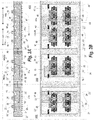
- Figs. 2A and 2B show transistor layouts of the exemplary inverter circuit for arrangement within the previously discussed clock-gated logic circuit region 130 of the integrated circuit in three different fully depleted Silicon on Insulator (FD SOI) CMOS process technologies for comparison purposes.
- Fig. 2A shows three sagittal cut-through views through the semiconductor substrate of the exemplary inverter circuit in the different CMOS processes.
- Fig. 2B shows schematically the corresponding top view layouts of the exemplary inverter circuits of the integrated semiconductor circuit.
- FD SOI fully depleted Silicon on Insulator
- Section 200 of Fig. 2A shows the layout of the exemplary inverter circuit integrated in a so-called standard well FD SOI process.
- the inverter circuit or inverter comprises a PMOS transistor arranged in an N-well diffusion 21 of a P-polarity semiconductor substrate 20 and an NMOS transistor arranged in an P-Well diffusion or region 22.
- The-P-well diffusion or region 22 is arranged at least partly within the N-well diffusion.
- a deep N-well 21a diffusion if formed vertically below the P-well diffusion 22 abutting the N-well diffusion 21.
- the gate terminal 23 of the PMOS transistor and the gate terminal 23 of the NMOS transistor are electrically connected via a polysilicon gate layer 23 to form an input terminal of the inverter circuit as illustrated on Fig.
- the drain terminal 25 of the PMOS transistor and the drain terminal 25 of the NMOS transistor are electrically connected via a metal layer to form an output terminal of the inverter circuit as illustrated on Fig. 2B .
- Respective gate oxides are arranged below the gate terminals 23 of the PMOS transistor and NMOS transistor.
- Channel regions 26 are formed below the respective gate oxides of the PMOS transistor and NMOS transistor.
- the semiconductor substrate 20 additionally comprises an ultra-thin buried oxide layer 27 arranged below respective drain diffusions 25, source diffusions 24 and gate channels 26 of the NMOS and PMOS transistors.
- This ultra-thin buried oxide layer 27 insulates these diffusion regions from the P-substrate 20 and N-well and P-well diffusions and largely eliminates their parasitic capacitances to the substrate and wells leading to lower switching losses and higher switching speeds of the gate circuit.
- This ultra-thin buried oxide layer 27 also eliminates the electrical connections of the respective bodies of the NMOS transistor and PMOS transistor from the negative supply voltage V CC and the positive supply voltage V DD allowing significant adjustments of the respective body voltages to very effectively control the respective threshold voltages of the NMOS and PMOS transistors leading to the above discussed advantageous reduction of leakage power in the inactive state of the clock-gated logic circuit region 130.
- the PMOS transistor comprises a body terminal or connection 22' which is connected to the N-well 21.
- the body terminal or connection 22' which is connected to the previously discussed first back bias voltage grid of the region 130 for receipt of the first back bias voltage V BP - for example through the first back bias input 115.
- the first back bias voltage V BP is supplied by the controllable back bias voltage generator 120.
- the NMOS transistor comprises a body terminal or connection 10 which is connected to the previously discussed second back bias voltage grid of the region 130 for receipt of the second back bias voltage V BN - for example through the second back bias input 113.
- the second back bias voltage V BN is also supplied by the controllable back bias voltage generator 120.
- Section 300 of Fig. 2A and Fig. 2B show transistor layouts of the exemplary inverter circuit integrated in a so-called flip-well FD SOI process. This inverter circuit implementation is described in detail below with reference to Figs. 3A and 3B .
- Section 400 of Fig. 2A and Fig. 2B shows the layout of two exemplary inverter circuits Inv1 and Inv2 integrated in a so-called mirrored flip-well FD SOI process.
- Each of the inverter circuits Inv1 and Inv2 comprises a PMOS transistor arranged in a P-well diffusion 42 within a surrounding N-well diffusion 41 and deep N-well diffusion 41a.
- the N-well diffusion 41 and deep N-well diffusion 41a are formed in a P-polarity semiconductor substrate 20.
- Each of the inverter circuits Inv1 and Inv2 furthermore comprises an NMOS transistor arranged in the N-well diffusion 41, but on opposite sides of the two PMOS transistors.
- the respective gate terminals 43a of the PMOS and NMOS transistors of the first inverter circuit Inv1 are electrically connected via a polysilicon gate layer 43a to form an input terminal of the first inverter circuit as best illustrated on Fig. 2B .
- the gate terminals 43b of the PMOS and NMOS transistors of the second inverter circuit Inv2 are electrically connected via a polysilicon gate layer 43b to form an input terminal of the second inverter circuit as best illustrated on Fig. 2B .
- the drain terminals 45 of the PMOS transistor and the drain terminal 45 of the NMOS transistor of the first inverter circuit Inv1 are electrically connected via a metal layer to form an output terminal of the first inverter circuit and the corresponding connection is made of drain terminals of the second inverter circuit Inv2 to form an output terminal of the second inverter circuit as best illustrated on Fig. 2B .
- Respective gate oxides are arranged below the gate terminals 43 of the PMOS transistor and NMOS transistor.
- Channel regions 46 are formed below the respective gate oxides of the PMOS transistors and NMOS transistors of the first and second inverter circuits.
- the semiconductor substrate 20 comprises an ultra-thin buried oxide layer 47 arranged below respective drain diffusions 45, source diffusions 44 and gate channels 36 of the NMOS and PMOS transistors of the first and second inverter circuits.
- This ultra-thin buried oxide layer 47 insulates these diffusion regions from the P-well diffusion 42 and the N-well diffusion 41 and largely eliminates their parasitic capacitances to the wells and/or P-substrate 20 leading to lower switching losses and higher switching speeds of the gate circuit.
- This ultra-thin buried oxide layer 27 also eliminates the electrical connections of the respective bodies of the NMOS transistors and PMOS transistors of the first and second inverter circuits from the negative supply voltage V CC and the positive supply voltage V DD allowing significant adjustments of the respective body voltages to very effectively control the respective threshold voltages of the NMOS and PMOS transistors of the leading to the above discussed advantageous reduction of leakage power in the inactive state of the clock-gated logic circuit region 130.
- the PMOS transistors share a body terminal or connection 42' which is connected to the shared P-well diffusion 42'.
- the body terminal or connection 42' is connected to the previously discussed first back bias voltage grid of the region 130 for receipt of the first back bias voltage V BP - for example through the first back bias input 115.
- the first back bias voltage V BP is supplied by the controllable back bias voltage generator 120.
- the NMOS transistors comprise one or several body terminal(s) or connection(s) 10 which is/are connected to the shared N-well diffusion 41 and deep N-well diffusion 41a.
- the body terminal or connection 10 is connected to the previously discussed second back bias voltage grid of the logic region 130 for receipt of the second back bias voltage V BN - for example through the second back bias input 113.
- the second back bias voltage V BN is also supplied by the controllable back bias voltage generator 120.
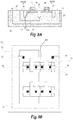
- Fig. 3A and Fig. 3B show transistor layouts of the exemplary inverter circuit as integrated in the previously mentioned flip-well FD SOI process.
- the inverter circuit comprises a PMOS transistor arranged in a P-well diffusion 32 within a surrounding N-well diffusion 31 and deep N-well diffusion 31a.
- the N-well diffusion 31 and deep N-well diffusion 31a are formed in a P-polarity semiconductor substrate 20.
- the inverter circuit furthermore comprises an NMOS transistor arranged in the N-well diffusion 31.
- the respective gate terminals 33a of the PMOS and NMOS transistors of the inverter circuit are electrically connected via a polysilicon gate layer 33a to form an input terminal of the inverter circuit as best illustrated on Fig. 4B .
- the drain terminals 35 of the PMOS transistor and the drain terminal 35 of the NMOS transistor are electrically connected via a metal layer to form an output terminal of the inverter circuit as best illustrated on Fig. 4B .
- Respective gate oxides 36 are arranged below the gate terminals 33 of the PMOS transistor and NMOS transistor. Channel regions are formed below the respective gate oxides of the PMOS and NMOS transistor.
- the semiconductor substrate 20 comprises an ultra-thin buried oxide layer 37 arranged below respective drain diffusions 35, respective source diffusions 34 and respective gate channels of the NMOS and PMOS transistors.
- This ultra-thin buried oxide layer 37 insulates the source and drain diffusion regions from the P-well diffusion 32 and the N-well diffusion 31 and largely eliminates their parasitic capacitances to the respective wells and/or P-substrate 20 leading to lower switching losses and higher switching speeds of the gate circuit.
- This ultra-thin buried oxide layer 37 also eliminates the electrical connections of the respective bodies of the NMOS transistors and PMOS transistors of the inverter circuit from the negative supply voltage V CC and the positive supply voltage V DD allowing significant adjustments of the respective body voltages to very effectively control the respective threshold voltages of the NMOS and PMOS transistors of the leading to the above discussed advantageous reduction of leakage power in the inactive state of the clock-gated logic circuit region 130.
- the PMOS transistor comprises body terminal or connection 32' which is connected to the P-well diffusion 32.
- the body terminal or connection 32' is connected to the previously discussed first back bias voltage grid of the region 130 for receipt of the first back bias voltage V BP - for example through the first back bias input 115.
- the first back bias voltage V BP is supplied by the controllable back bias voltage generator 120.
- the NMOS transistors comprise one or several body terminal(s) or connection(s) 10 which is/are connected to the N-well diffusion 31 and deep N-well diffusion 31a.
- the body terminal or connection 10 is connected to the previously discussed second back bias voltage grid of the logic region 130 for receipt of the second back bias voltage V BN - for example through the second back bias input 113.
- the second back bias voltage V BN is also supplied by the controllable back bias voltage generator 120.
- the second back bias voltage V BN preferably is maximally 300 mV, for example 100 mV or 200 mV, lower than the negative DC supply voltage (which is connected to the source terminal 34 of the NMOS transistor). This voltage difference will typically prevent any massive flow of leakage current from the body terminal 10 into the underlying P-substrate due to the creation of a forward biased diode junction.
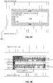
- Fig. 4A shows schematically an exemplary small cell area floorplan of the previously discussed clock-gated logic circuit region 130, associated clock gating circuitry 110 and a controllable back bias voltage generator 120 of the integrated semiconductor circuit 500 fabricated in the previously discussed flip-well FD SOI process.
- the controllable back bias voltage generator 120 of the illustrated small cell area floorplan utilizes a first back bias voltage for bodies of the PMOS transistors of the gated logic circuit region 130 and a second back bias voltage for bodies of the NMOS transistors of the gated logic circuit region 130.
- a plurality of well and substrate isolation cells 150 at least partly surround logic circuitry of the gated logic circuit region 130.
- Fig. 4B shows schematically an exemplary small cell area floorplan of the previously discussed clock-gated logic circuit region 130, associated clock gating circuitry 110 and a controllable back bias voltage generator 120 on the integrated semiconductor circuit 500 fabricated in the previously discussed flip-well FD SOI process.
- the clock-gated logic circuit region 130 comprises a P-well isolated back-biasing region surrounded by globally back-biased logic areas.
- the controllable back bias voltage generator 120 of the illustrated small cell area floorplan utilizes only an adjustable back bias voltage for bodies of the PMOS transistors of the gated logic circuit region 130. This feature eliminates any need for full substrate isolation as the PMOS transistors are arranged in their own well diffusion or region 250 and therefore isolated from the substrate.
- the small cell area floorplan includes dedicated cells "P-well isolator Cells" which serve to electrically insulate the P-well region 250 from the remaining portion of the standard cell row.
Landscapes
- Engineering & Computer Science (AREA)
- Theoretical Computer Science (AREA)
- Physics & Mathematics (AREA)
- General Engineering & Computer Science (AREA)
- General Physics & Mathematics (AREA)
- Computing Systems (AREA)
- Computer Hardware Design (AREA)
- Mathematical Physics (AREA)
- Power Engineering (AREA)
- Semiconductor Integrated Circuits (AREA)
- Thin Film Transistor (AREA)
- Logic Circuits (AREA)
- Metal-Oxide And Bipolar Metal-Oxide Semiconductor Integrated Circuits (AREA)
Claims (17)
- Hörgerät, umfassend eine integrierte Halbleiterschaltung (100), wobei die integrierte Halbleiterschaltung (100) umfasst:- eine Steuer- und Verarbeitungsschaltung, die umfasst:
einen ersten Audioeingangskanal zum Empfangen eines ersten Audiosignals,- einen Signalprozessor zum Empfangen und Verarbeiten des ersten Audiosignals zum Erzeugen eines kompensierten Mikrofonsignals gemäß einem Hörverlust eines Benutzers;- einen Ausgangsverstärker zum Empfangen des kompensierten Mikrofonsignals und Erzeugen eines verstärkten oder gepufferten Ausgangssignals zur Anwendung an einem Miniaturempfänger oder Lautsprecher des Hörgeräts;dadurch gekennzeichnet, dass die integrierte Halbleiterschaltung (100) weiterhin umfasst:- ein Taktsignalgitter (102) zum Verteilen eines Taktsignals (Clk) auf einen oder mehrere Logikschaltungsbereiche,- einen ersten Logikschaltungsbereich (130), der durch eine positive DC-Versorgungsspannung (VDD) und eine negative DC-Versorgungsspannung (VCC) versorgt wird;- wobei der erste Logikschaltungsbereich (130) umfasst:- ein erstes Bereichs-Taktnetzwerk zum Bereitstellen eines ersten Bereichs-Taktsignals (R-Clk) an eine oder mehrere digitale Logikschaltungen des ersten Logikschaltungsbereichs (130),- eine Taktgeberschaltung (110), die konfiguriert ist, das erste Bereichs-Taktsignal (R-Clk) aus dem Taktsignal (Clk) abzuleiten und das erste Bereichs-Taktsignal (R-Clk) nach einem Zustandsauswahlsignal (En) des ersten Logikschaltungsbereichs (130) selektiv anzuwenden und zu unterbrechen,- ein erstes rückseitiges Biasspannungsnetz, das mit entsprechenden Körpern von PMOS-Transistoren der einen oder mehreren digitalen Logikschaltungen verbunden ist, und ein zweites rückseitiges Biasspannungsnetz, das mit entsprechenden Körpern von NMOS-Transistoren der einen oder mehreren digitalen Logikschaltungen verbunden ist,- einen steuerbaren rückseitige Biasspannungsgenerator (130), der konfiguriert ist zum:- Einstellen einer ersten rückseitigen Biasspannung (VBP) des ersten rückseitigen Biasspannungsnetzes zwischen einem ersten Pegel und einem zweiten Pegel gemäß dem Zustandsauswahlsignal (En); und- Einstellen einer zweiten rückseitigen Biasspannung (VBN) des zweiten rückseitigen Biasspannungsnetzes zwischen einem ersten Pegel und einem zweiten Pegel gemäß dem Zustandsauswahlsignal (En). - Hörgerät nach Anspruch 1, wobei die eine oder die mehreren digitale(n) Logikschaltung(en) der integrierten Halbleiterschaltung (100) mindestens eine sequentielle Logikschaltung, wie beispielsweise einen Flip-Flop, umfassen, die mit dem ersten Bereichs-Taktnetzwerk zum Empfangen des ersten Bereichs-Taktsignals (R-Clk) verbunden ist.
- Hörgerät nach Anspruch 1 oder 2, wobei das Zustandsauswahlsignal (En) der integrierten Halbleiterschaltung (100) konfiguriert ist, den ersten Logikschaltungsbereich (130) zwischen einem aktiven Zustand, in dem das erste Bereichs-Taktsignal (R-Clk) aktiv ist, und einem inaktiven Zustand, in dem das erste Bereichs-Taktsignal (R-Clk) unterbrochen oder nicht geschaltet ist, zu schalten.
- Hörgerät nach Anspruch 3, wobei der steuerbare rückseitige Biasspannungsgenerator (120) der integrierten Halbleiterschaltung (100) konfiguriert ist, um:- im aktiven Zustand: Die erste Biasspannung (VBP) des ersten rückseitigen Biasspannungsnetzes auf die positive DC-Versorgungsspannung (VDD) einzustellen und die Biasspannung (VBN) des zweiten rückseitigen Biasspannungsnetzes auf die negative DC-Versorgungsspannung (VCC) einzustellen; und- im inaktiven Zustand: Die Biasspannung des ersten rückseitigen Biasspannungsnetzes auf eine Spannung oberhalb der positiven DC-Versorgungsspannung (VDD) einzustellen und die Biasspannung des zweiten rückseitigen Biasspannungsnetzes auf eine Spannung unterhalb der negativen DC-Versorgungsspannung (VCC) einzustellen.
- Hörgerät nach einem der vorstehenden Ansprüche, wobei der steuerbare rückseitige Biasspannungsgenerator der integrierten Halbleiterschaltung (100) konfiguriert ist zum:- Einstellen einer Spannungsdifferenz zwischen dem ersten Pegel und dem zweiten Pegel des ersten rückseitigen Biasspannungsnetzes größer als 100 mV, bevorzugter mindestens 200 mV; und- Einstellen einer Spannungsdifferenz zwischen dem ersten Pegel und dem zweiten Pegel des zweiten rückseitigen Biasspannungsnetzes größer als 100 mV, bevorzugter mindestens 200 mV.
- Hörgerät nach einem der vorstehenden Ansprüche, wobei der steuerbare rückseitige Biasspannungsgenerator der integrierten Halbleiterschaltung (100) umfasst:- einen ersten Multiplexer, der konfiguriert ist, selektiv eine erste rückseitige Biasspannung und die positive DC-Versorgungsspannung (VDD) mit dem ersten rückseitigen Biasspannungsnetz gemäß dem Zustandsauswahlsignal zu verbinden; und- einen zweiten Multiplexer, der konfiguriert ist, selektiv die zweite rückseitige Biasspannung und die negative DC-Versorgungsspannung (VCC) mit dem zweiten rückseitigen Biasspannungsnetz gemäß dem Zustandsauswahlsignal zu verbinden.
- Hörgerät nach Anspruch 6, wobei der erste Multiplexer der integrierten Halbleiterschaltung (100) umfasst:- einen ersten Eingang, der mit der ersten rückseitigen Biasspannung verbunden ist, und einen zweiten Eingang, der mit der positiven DC-Versorgungsspannung (VDD) verbunden ist,- einen Auswahleingang, der mit dem Zustandsauswahlsignal (En) gekoppelt ist,- einen Ausgang, der mit dem ersten rückseitigen Biasspannungsnetz verbunden ist; und wobei der zweite Multiplexer umfasst:- einen ersten Eingang, der mit der zweiten rückseitigen Biasspannung (VBN) verbunden ist, und einen zweiten Eingang, der mit der negativen DC-Versorgungsspannung (VCC) verbunden ist,- einen Auswahleingang, der mit dem Zustandsauswahlsignal (En) gekoppelt ist,- einen Ausgang, der mit dem zweiten rückseitigen Biasspannungsnetz verbunden ist.
- Hörgerät nach einem der Ansprüche 5-7, wobei der steuerbare rückseitige Biasspannungsgenerator der integrierten Halbleiterschaltung (100) umfasst:- einen ersten DC-DC-Wandler mit Schaltmodus, der konfiguriert ist, mindestens eine der ersten rückseitigen Biasspannung und der zweiten Biasspannung aus der positiven DC-Versorgungsspannung (VDD) zu erzeugen.
- Hörgerät nach Anspruch 7, wobei mindestens einer der ersten und zweiten DC-DC-Wandler mit Schaltmodus der integrierten Halbleiterschaltung (100) einen geschalteten Kondensatorwandler umfasst.
- Hörgerät nach einem der vorstehenden Ansprüche, wobei die Taktgeberschaltung (110) der integrierten Halbleiterschaltung (100) einen D-FF und ein UND-Gatter umfasst; wobei der D-FF einen Dateneingang aufweist, der mit dem Zustandsauswahlsignal verbunden ist, einen Takteingang, der mit dem Taktsignal verbunden ist, und einen Ausgang, der mit einem ersten Eingang des UND-Gatters verbunden ist, und einen zweiten Eingang des UND-Gatters, der mit dem Taktsignal verbunden ist, so dass der Ausgang des UND-Gatters das erste Bereichs-Taktsignal an das erste Bereichs-Taktsignalnetzwerk liefert.
- Hörgerät nach einem der vorstehenden Ansprüche, wobei die integrierte Halbleiterschaltung (100) auf einem vollständig verarmten Silizium-auf-einem-Isolator(FD SOI)-Halbleitersubstrat oder einem teilweise verarmten Silizium-auf-einem-Isolator(PD SOI)-Halbleitersubstrat angeordnet ist.
- Hörgerät nach Anspruch 11, wobei das vollständig oder teilweise verarmten Silizium-auf-einem-Isolator-Substrat der integrierten Halbleiterschaltung (100) eine Standard-Wannenstruktur umfasst; wobei die Standard-Wannenstruktur umfasst;- eine Vielzahl von N-Wannen, die entsprechende PMOS-Transistoren der einen oder mehreren digitalen Logikschaltungen umfassen, wobei die Vielzahl von N-Wannen mit dem zweiten rückseitigen Biasspannungsnetz zum Empfangen der zweiten rückseitigen Biasspannung verbunden ist; und- eine Vielzahl von P-Wannen, die entsprechende NMOS-Transistoren der einen oder mehreren digitalen Logikschaltungen umfassen, wobei die Vielzahl von P-Wannen mit dem ersten rückseitigen Biasspannungsnetz zum Empfangen der ersten rückseitigen Biasspannung verbunden ist.
- Hörgerät nach Anspruch 11, wobei das vollständig oder teilweise verarmten Silizium-auf-einem-Isolator-Substrat eine Flip-Well-Struktur umfasst; wobei die Flip-Well-Struktur umfasst;- eine Vielzahl von N-Wannen, die entsprechende NMOS-Transistoren der einen oder mehreren digitalen Logikschaltungen umfassen, wobei die Vielzahl von N-Wannen mit dem zweiten rückseitigen Biasspannungsnetz zum Empfangen der zweiten rückseitigen Biasspannung verbunden ist; und- eine Vielzahl von P-Wannen, die entsprechende PMOS-Transistoren der einen oder mehreren digitalen Logikschaltungen umfassen, wobei die Vielzahl von P-Wannen mit dem ersten rückseitigen Biasspannungsnetz zum Empfangen der ersten rückseitigen Biasspannung verbunden ist; undeine Vielzahl von tiefen n-Wannen-Diffusionen, die unter entsprechenden der Vielzahl von P-Wannen angeordnet sind.
- Hörgerät nach einem der Ansprüche 1-10, wobei die integrierte Halbleiterschaltung (100) ein CMOS-Massensubstrat umfasst, das eine Doppelwannenstruktur umfasst; wobei die Doppelwannenstruktur umfasst;- eine Vielzahl von N-Wannen, die entsprechende NMOS-Transistoren der einen oder mehreren digitalen Logikschaltungen umfassen, wobei die Vielzahl von N-Wannen mit dem zweiten rückseitigen Biasspannungsnetz zum Empfangen der zweiten rückseitigen Biasspannung (VBN) verbunden ist; und- eine Vielzahl von P-Wannen, die entsprechende PMOS-Transistoren der einen oder mehreren digitalen Logikschaltungen umfassen, wobei die Vielzahl von P-Wannen mit dem ersten rückseitigen Biasspannungsnetz zum Empfangen der ersten rückseitigen Biasspannung (VBP) verbunden ist; undeine Vielzahl von tiefen n-Wannen-Diffusionen, die unter entsprechenden der Vielzahl von P-Wannen angeordnet sind.
- Hörgerät nach einem der Ansprüche 1-14, wobei der Signalprozessor die einen oder mehreren Bereiche der Logikschaltung umfasst.
- Hörgerät nach einem der Ansprüche 1-15, wobei eine Taktfrequenz des Taktsignals (Clk) der integrierten Halbleiterschaltung (100) kleiner als 50 MHZ oder kleiner als 25 MHZ ist.
- Verfahren zum Steuern des Ableitstroms einer oder mehrerer digitaler Logikschaltungen eines ersten Logikschaltungsbereichs (130) einer integrierten Halbleiterschaltung (100) eines Hörgeräts, wobei das Hörgerät umfasst:- eine Steuer- und Verarbeitungsschaltung, die umfasst:
einen ersten Audioeingangskanal zum Empfangen eines ersten Audiosignals,- einen Signalprozessor zum Empfangen und Verarbeiten des ersten Audiosignals zum Erzeugen eines kompensierten Mikrofonsignals gemäß einem Hörverlust eines Benutzers;- einen Ausgangsverstärker zum Empfangen des kompensierten Mikrofonsignals und Erzeugen eines verstärkten oder gepufferten Ausgangssignals zur Anwendung an einem Miniatur-Empfänger oder Lautsprecher des Hörsystems; wobei das Verfahren umfasst:- Zuführen eines Taktsignals (Clk) und eines Zustandsauswahlsignals (En) zu einer Taktgeberschaltung (110),- Ableiten eines ersten Bereichs-Taktsignals (R-Clk) für den ersten Logikschaltungsbereich (130) aus dem Taktsignal (Clk) und dem Zustandsauswahlsignal (En),- Anwenden des ersten Bereichs-Taktsignals (R-Clk) an ein Bereichs-Taktnetzwerk des ersten Logikschaltungsbereichs (130) in einem aktiven Zustand des ersten Logikschaltungsbereichs (130),- Unterbrechen des ersten Bereichs-Taktsignals (R-Clk) in einem inaktiven Zustand des ersten Logikschaltungsbereichs (130),- Zuführen einer ersten rückseitigen Biasspannung (VBP) zu einem ersten rückseitigen Biasspannungsnetz, das mit Körpern von einer Vielzahl von PMOS-Transistoren der einen oder mehreren digitalen Logikschaltungen verbunden ist,- Zuführen einer zweiten rückseitigen Biasspannung (VBN) zu einem zweiten Biasspannungsnetz, das mit Körpern von NMOS-Transistoren der einen oder mehreren digitalen Logikschaltungen verbunden ist,- Einstellen der rückseitigen Biasspannung (VBP) des ersten rückseitigen Biasspannungsnetzes zwischen einem ersten Pegel und einem zweiten Pegel gemäß dem Zustandsauswahlsignal (En),- Einstellen der rückseitigen Biasspannung (VBN) des zweiten rückseitigen Biasspannungsnetzes zwischen einem ersten Pegel und einem zweiten Pegel gemäß dem Zustandsauswahlsignal (En).
Priority Applications (5)
| Application Number | Priority Date | Filing Date | Title |
|---|---|---|---|
| EP16206966.0A EP3343769B1 (de) | 2016-12-27 | 2016-12-27 | Integrierte schaltung mit verstellbarer sperrvorspannung von einer oder mehreren logikschaltungsregionen |
| DK16206966.0T DK3343769T3 (da) | 2016-12-27 | 2016-12-27 | Integreret kredsløb, der omfatter justerbar spærreforspænding af én eller flere logiske kredsløbsregioner |
| US15/676,907 US10181855B2 (en) | 2016-12-27 | 2017-08-14 | Integrated circuit comprising adjustable back biasing of one or more logic circuit regions |
| JP2017249986A JP2018137429A (ja) | 2016-12-27 | 2017-12-26 | 1つ以上の論理回路領域の調節可能なバックバイアス特性を有する集積回路 |
| CN201711431161.6A CN108242924B (zh) | 2016-12-27 | 2017-12-26 | 包括一个或多个逻辑电路区域的可调反向偏压的集成电路 |
Applications Claiming Priority (1)
| Application Number | Priority Date | Filing Date | Title |
|---|---|---|---|
| EP16206966.0A EP3343769B1 (de) | 2016-12-27 | 2016-12-27 | Integrierte schaltung mit verstellbarer sperrvorspannung von einer oder mehreren logikschaltungsregionen |
Publications (2)
| Publication Number | Publication Date |
|---|---|
| EP3343769A1 EP3343769A1 (de) | 2018-07-04 |
| EP3343769B1 true EP3343769B1 (de) | 2019-02-06 |
Family
ID=57749745
Family Applications (1)
| Application Number | Title | Priority Date | Filing Date |
|---|---|---|---|
| EP16206966.0A Active EP3343769B1 (de) | 2016-12-27 | 2016-12-27 | Integrierte schaltung mit verstellbarer sperrvorspannung von einer oder mehreren logikschaltungsregionen |
Country Status (5)
| Country | Link |
|---|---|
| US (1) | US10181855B2 (de) |
| EP (1) | EP3343769B1 (de) |
| JP (1) | JP2018137429A (de) |
| CN (1) | CN108242924B (de) |
| DK (1) | DK3343769T3 (de) |
Families Citing this family (2)
| Publication number | Priority date | Publication date | Assignee | Title |
|---|---|---|---|---|
| US10739807B2 (en) * | 2018-09-11 | 2020-08-11 | Stmicroelectronics (Crolles 2) Sas | Body biasing for ultra-low voltage digital circuits |
| US11336246B1 (en) * | 2021-03-25 | 2022-05-17 | Taiwan Semiconductor Manufacturing Company, Ltd. | Amplifier circuit |
Family Cites Families (32)
| Publication number | Priority date | Publication date | Assignee | Title |
|---|---|---|---|---|
| JP3184265B2 (ja) * | 1991-10-17 | 2001-07-09 | 株式会社日立製作所 | 半導体集積回路装置およびその制御方法 |
| US5461338A (en) * | 1992-04-17 | 1995-10-24 | Nec Corporation | Semiconductor integrated circuit incorporated with substrate bias control circuit |
| JPH0828965B2 (ja) * | 1992-09-02 | 1996-03-21 | 日本電気株式会社 | 電圧変換回路 |
| KR0169157B1 (ko) * | 1993-11-29 | 1999-02-01 | 기다오까 다까시 | 반도체 회로 및 mos-dram |
| JP3641511B2 (ja) * | 1995-06-16 | 2005-04-20 | 株式会社ルネサステクノロジ | 半導体装置 |
| KR100568075B1 (ko) * | 1996-11-26 | 2006-10-24 | 가부시끼가이샤 히다치 세이사꾸쇼 | 반도체집적회로장치 |
| JPH10261946A (ja) * | 1997-03-19 | 1998-09-29 | Mitsubishi Electric Corp | 半導体集積回路 |
| KR100243295B1 (ko) * | 1997-06-26 | 2000-02-01 | 윤종용 | 반도체장치의 백 바이어스 발생기 및 그 발생방법 |
| JP3814385B2 (ja) * | 1997-10-14 | 2006-08-30 | 株式会社ルネサステクノロジ | 半導体集積回路装置 |
| US6100567A (en) * | 1998-06-11 | 2000-08-08 | Sun Microsystems, Inc. | Tunable threshold SOI device using back gate and intrinsic channel region |
| TW453032B (en) * | 1998-09-09 | 2001-09-01 | Hitachi Ltd | Semiconductor integrated circuit apparatus |
| JP3928837B2 (ja) * | 1999-09-13 | 2007-06-13 | 株式会社ルネサステクノロジ | 半導体集積回路装置 |
| JP2001156619A (ja) * | 1999-11-25 | 2001-06-08 | Texas Instr Japan Ltd | 半導体回路 |
| JP3485885B2 (ja) * | 2000-12-11 | 2004-01-13 | 三洋電機株式会社 | 半導体集積回路装置の設計方法 |
| WO2002065642A1 (en) * | 2001-02-15 | 2002-08-22 | Hitachi,Ltd | Semiconductor integrated circuit, data processing system, and mobile communication terminal apparatus |
| JP4027279B2 (ja) * | 2002-07-19 | 2007-12-26 | 株式会社ルネサステクノロジ | 半導体集積回路装置 |
| JP4583781B2 (ja) * | 2003-06-12 | 2010-11-17 | アルパイン株式会社 | 音声補正装置 |
| JP2009500959A (ja) * | 2005-07-08 | 2009-01-08 | ズィーモス テクノロジー,インコーポレイテッド | ソース・トランジスター構成及び制御方法 |
| US7323909B2 (en) * | 2005-07-29 | 2008-01-29 | Sequence Design, Inc. | Automatic extension of clock gating technique to fine-grained power gating |
| US7330049B2 (en) * | 2006-03-06 | 2008-02-12 | Altera Corporation | Adjustable transistor body bias generation circuitry with latch-up prevention |
| JP2008153415A (ja) * | 2006-12-18 | 2008-07-03 | Renesas Technology Corp | 半導体集積回路およびその製造方法 |
| JP5049691B2 (ja) * | 2007-08-06 | 2012-10-17 | 株式会社日立製作所 | 半導体集積回路 |
| WO2009076949A1 (en) * | 2007-12-19 | 2009-06-25 | Widex A/S | Hearing aid and a method of operating a hearing aid |
| JP2010045483A (ja) * | 2008-08-11 | 2010-02-25 | Nec Electronics Corp | クロックゲーティング回路 |
| CN106887950B (zh) * | 2009-12-01 | 2020-12-11 | 天工方案公司 | 电压转换系统 |
| JP5443623B2 (ja) * | 2010-02-26 | 2014-03-19 | ヴェーデクス・アクティーセルスカプ | 適応バルクバイアス電力管理を備える補聴器 |
| US20120151226A1 (en) * | 2010-12-12 | 2012-06-14 | Via Technologies, Inc. | Apparatus and method for selective back bias control of an integrated circuit |
| WO2013018217A1 (ja) * | 2011-08-03 | 2013-02-07 | 富士通株式会社 | 半導体集積回路及びラッチ回路の駆動方法 |
| DE102013207324A1 (de) * | 2012-05-11 | 2013-11-14 | Semiconductor Energy Laboratory Co., Ltd. | Halbleitervorrichtung und elektronisches Gerät |
| KR102095856B1 (ko) * | 2013-04-15 | 2020-04-01 | 삼성전자주식회사 | 반도체 메모리 장치 및 그것의 바디 바이어스 방법 |
| US9455689B2 (en) * | 2013-11-20 | 2016-09-27 | Stmicroelectronics Sa | Current source array |
| US9312834B1 (en) * | 2015-01-08 | 2016-04-12 | Freescale Semiconductors,Inc. | Low leakage flip-flop circuit |
-
2016
- 2016-12-27 EP EP16206966.0A patent/EP3343769B1/de active Active
- 2016-12-27 DK DK16206966.0T patent/DK3343769T3/da active
-
2017
- 2017-08-14 US US15/676,907 patent/US10181855B2/en active Active
- 2017-12-26 CN CN201711431161.6A patent/CN108242924B/zh active Active
- 2017-12-26 JP JP2017249986A patent/JP2018137429A/ja not_active Ceased
Non-Patent Citations (1)
| Title |
|---|
| None * |
Also Published As
| Publication number | Publication date |
|---|---|
| CN108242924A (zh) | 2018-07-03 |
| US10181855B2 (en) | 2019-01-15 |
| CN108242924B (zh) | 2023-06-02 |
| JP2018137429A (ja) | 2018-08-30 |
| DK3343769T3 (da) | 2019-05-06 |
| US20180183440A1 (en) | 2018-06-28 |
| EP3343769A1 (de) | 2018-07-04 |
Similar Documents
| Publication | Publication Date | Title |
|---|---|---|
| KR100302535B1 (ko) | 가변 임계 전압을 가지는 soi형 반도체 장치 및 바이어스전압발생장치 | |
| JP3579633B2 (ja) | 半導体集積回路 | |
| US7800405B2 (en) | Passgate structures for use in low-voltage applications | |
| CN210780725U (zh) | 电路 | |
| US20100090282A1 (en) | Semiconductor integrated circuit | |
| US6297686B1 (en) | Semiconductor integrated circuit for low-voltage high-speed operation | |
| US20190273486A1 (en) | Semiconductor device | |
| EP3343769B1 (de) | Integrierte schaltung mit verstellbarer sperrvorspannung von einer oder mehreren logikschaltungsregionen | |
| US8723592B2 (en) | Adjustable body bias circuit | |
| JP4799255B2 (ja) | 半導体集積回路 | |
| JP2008034667A (ja) | 半導体集積回路装置 | |
| JP2005175269A (ja) | 半導体装置 | |
| US8020018B2 (en) | Circuit arrangement and method of operating a circuit arrangement | |
| CN103988434A (zh) | 用于功率切换的方法和装置 | |
| US20070085146A1 (en) | Semiconductor integrated circuit | |
| JPH0936246A (ja) | 半導体装置 | |
| US6538493B2 (en) | Semiconductor integrated circuit | |
| JP2018019333A (ja) | 半導体スイッチング回路 | |
| US7906990B2 (en) | Semiconductor integrated circuit device | |
| EP4283872A2 (de) | Pegelschieberschaltung mit durch backgate gesteuerten transistoren | |
| Prabhat et al. | A bulk 65nm Cortex-M0+ SoC with all-digital forward body bias for 4.3 X subthreshold speedup | |
| JP2007019811A (ja) | ドミノcmos論理回路 | |
| JP4212140B2 (ja) | ゲートアレイ | |
| US10115452B2 (en) | Semiconductor device | |
| JP3698852B2 (ja) | 半導体集積回路 |
Legal Events
| Date | Code | Title | Description |
|---|---|---|---|
| PUAI | Public reference made under article 153(3) epc to a published international application that has entered the european phase |
Free format text: ORIGINAL CODE: 0009012 |
|
| STAA | Information on the status of an ep patent application or granted ep patent |
Free format text: STATUS: THE APPLICATION HAS BEEN PUBLISHED |
|
| STAA | Information on the status of an ep patent application or granted ep patent |
Free format text: STATUS: REQUEST FOR EXAMINATION WAS MADE |
|
| AK | Designated contracting states |
Kind code of ref document: A1 Designated state(s): AL AT BE BG CH CY CZ DE DK EE ES FI FR GB GR HR HU IE IS IT LI LT LU LV MC MK MT NL NO PL PT RO RS SE SI SK SM TR |
|
| AX | Request for extension of the european patent |
Extension state: BA ME |
|
| 17P | Request for examination filed |
Effective date: 20180601 |
|
| RBV | Designated contracting states (corrected) |
Designated state(s): AL AT BE BG CH CY CZ DE DK EE ES FI FR GB GR HR HU IE IS IT LI LT LU LV MC MK MT NL NO PL PT RO RS SE SI SK SM TR |
|
| GRAP | Despatch of communication of intention to grant a patent |
Free format text: ORIGINAL CODE: EPIDOSNIGR1 |
|
| STAA | Information on the status of an ep patent application or granted ep patent |
Free format text: STATUS: GRANT OF PATENT IS INTENDED |
|
| INTG | Intention to grant announced |
Effective date: 20180725 |
|
| GRAJ | Information related to disapproval of communication of intention to grant by the applicant or resumption of examination proceedings by the epo deleted |
Free format text: ORIGINAL CODE: EPIDOSDIGR1 |
|
| STAA | Information on the status of an ep patent application or granted ep patent |
Free format text: STATUS: REQUEST FOR EXAMINATION WAS MADE |
|
| GRAR | Information related to intention to grant a patent recorded |
Free format text: ORIGINAL CODE: EPIDOSNIGR71 |
|
| GRAS | Grant fee paid |
Free format text: ORIGINAL CODE: EPIDOSNIGR3 |
|
| STAA | Information on the status of an ep patent application or granted ep patent |
Free format text: STATUS: GRANT OF PATENT IS INTENDED |
|
| INTC | Intention to grant announced (deleted) | ||
| GRAA | (expected) grant |
Free format text: ORIGINAL CODE: 0009210 |
|
| STAA | Information on the status of an ep patent application or granted ep patent |
Free format text: STATUS: THE PATENT HAS BEEN GRANTED |
|
| INTG | Intention to grant announced |
Effective date: 20181210 |
|
| AK | Designated contracting states |
Kind code of ref document: B1 Designated state(s): AL AT BE BG CH CY CZ DE DK EE ES FI FR GB GR HR HU IE IS IT LI LT LU LV MC MK MT NL NO PL PT RO RS SE SI SK SM TR |
|
| REG | Reference to a national code |
Ref country code: GB Ref legal event code: FG4D |
|
| REG | Reference to a national code |
Ref country code: CH Ref legal event code: EP Ref country code: AT Ref legal event code: REF Ref document number: 1095497 Country of ref document: AT Kind code of ref document: T Effective date: 20190215 |
|
| REG | Reference to a national code |
Ref country code: IE Ref legal event code: FG4D |
|
| REG | Reference to a national code |
Ref country code: DE Ref legal event code: R096 Ref document number: 602016009814 Country of ref document: DE |
|
| REG | Reference to a national code |
Ref country code: DK Ref legal event code: T3 Effective date: 20190429 |
|
| REG | Reference to a national code |
Ref country code: NL Ref legal event code: MP Effective date: 20190206 |
|
| REG | Reference to a national code |
Ref country code: LT Ref legal event code: MG4D |
|
| PG25 | Lapsed in a contracting state [announced via postgrant information from national office to epo] |
Ref country code: PT Free format text: LAPSE BECAUSE OF FAILURE TO SUBMIT A TRANSLATION OF THE DESCRIPTION OR TO PAY THE FEE WITHIN THE PRESCRIBED TIME-LIMIT Effective date: 20190606 Ref country code: LT Free format text: LAPSE BECAUSE OF FAILURE TO SUBMIT A TRANSLATION OF THE DESCRIPTION OR TO PAY THE FEE WITHIN THE PRESCRIBED TIME-LIMIT Effective date: 20190206 Ref country code: NL Free format text: LAPSE BECAUSE OF FAILURE TO SUBMIT A TRANSLATION OF THE DESCRIPTION OR TO PAY THE FEE WITHIN THE PRESCRIBED TIME-LIMIT Effective date: 20190206 Ref country code: FI Free format text: LAPSE BECAUSE OF FAILURE TO SUBMIT A TRANSLATION OF THE DESCRIPTION OR TO PAY THE FEE WITHIN THE PRESCRIBED TIME-LIMIT Effective date: 20190206 Ref country code: NO Free format text: LAPSE BECAUSE OF FAILURE TO SUBMIT A TRANSLATION OF THE DESCRIPTION OR TO PAY THE FEE WITHIN THE PRESCRIBED TIME-LIMIT Effective date: 20190506 Ref country code: SE Free format text: LAPSE BECAUSE OF FAILURE TO SUBMIT A TRANSLATION OF THE DESCRIPTION OR TO PAY THE FEE WITHIN THE PRESCRIBED TIME-LIMIT Effective date: 20190206 |
|
| REG | Reference to a national code |
Ref country code: AT Ref legal event code: MK05 Ref document number: 1095497 Country of ref document: AT Kind code of ref document: T Effective date: 20190206 |
|
| PG25 | Lapsed in a contracting state [announced via postgrant information from national office to epo] |
Ref country code: BG Free format text: LAPSE BECAUSE OF FAILURE TO SUBMIT A TRANSLATION OF THE DESCRIPTION OR TO PAY THE FEE WITHIN THE PRESCRIBED TIME-LIMIT Effective date: 20190506 Ref country code: IS Free format text: LAPSE BECAUSE OF FAILURE TO SUBMIT A TRANSLATION OF THE DESCRIPTION OR TO PAY THE FEE WITHIN THE PRESCRIBED TIME-LIMIT Effective date: 20190606 Ref country code: GR Free format text: LAPSE BECAUSE OF FAILURE TO SUBMIT A TRANSLATION OF THE DESCRIPTION OR TO PAY THE FEE WITHIN THE PRESCRIBED TIME-LIMIT Effective date: 20190507 Ref country code: RS Free format text: LAPSE BECAUSE OF FAILURE TO SUBMIT A TRANSLATION OF THE DESCRIPTION OR TO PAY THE FEE WITHIN THE PRESCRIBED TIME-LIMIT Effective date: 20190206 Ref country code: LV Free format text: LAPSE BECAUSE OF FAILURE TO SUBMIT A TRANSLATION OF THE DESCRIPTION OR TO PAY THE FEE WITHIN THE PRESCRIBED TIME-LIMIT Effective date: 20190206 Ref country code: HR Free format text: LAPSE BECAUSE OF FAILURE TO SUBMIT A TRANSLATION OF THE DESCRIPTION OR TO PAY THE FEE WITHIN THE PRESCRIBED TIME-LIMIT Effective date: 20190206 |
|
| PG25 | Lapsed in a contracting state [announced via postgrant information from national office to epo] |
Ref country code: CZ Free format text: LAPSE BECAUSE OF FAILURE TO SUBMIT A TRANSLATION OF THE DESCRIPTION OR TO PAY THE FEE WITHIN THE PRESCRIBED TIME-LIMIT Effective date: 20190206 Ref country code: RO Free format text: LAPSE BECAUSE OF FAILURE TO SUBMIT A TRANSLATION OF THE DESCRIPTION OR TO PAY THE FEE WITHIN THE PRESCRIBED TIME-LIMIT Effective date: 20190206 Ref country code: AL Free format text: LAPSE BECAUSE OF FAILURE TO SUBMIT A TRANSLATION OF THE DESCRIPTION OR TO PAY THE FEE WITHIN THE PRESCRIBED TIME-LIMIT Effective date: 20190206 Ref country code: ES Free format text: LAPSE BECAUSE OF FAILURE TO SUBMIT A TRANSLATION OF THE DESCRIPTION OR TO PAY THE FEE WITHIN THE PRESCRIBED TIME-LIMIT Effective date: 20190206 Ref country code: SK Free format text: LAPSE BECAUSE OF FAILURE TO SUBMIT A TRANSLATION OF THE DESCRIPTION OR TO PAY THE FEE WITHIN THE PRESCRIBED TIME-LIMIT Effective date: 20190206 Ref country code: IT Free format text: LAPSE BECAUSE OF FAILURE TO SUBMIT A TRANSLATION OF THE DESCRIPTION OR TO PAY THE FEE WITHIN THE PRESCRIBED TIME-LIMIT Effective date: 20190206 Ref country code: EE Free format text: LAPSE BECAUSE OF FAILURE TO SUBMIT A TRANSLATION OF THE DESCRIPTION OR TO PAY THE FEE WITHIN THE PRESCRIBED TIME-LIMIT Effective date: 20190206 |
|
| REG | Reference to a national code |
Ref country code: DE Ref legal event code: R097 Ref document number: 602016009814 Country of ref document: DE |
|
| PG25 | Lapsed in a contracting state [announced via postgrant information from national office to epo] |
Ref country code: SM Free format text: LAPSE BECAUSE OF FAILURE TO SUBMIT A TRANSLATION OF THE DESCRIPTION OR TO PAY THE FEE WITHIN THE PRESCRIBED TIME-LIMIT Effective date: 20190206 Ref country code: PL Free format text: LAPSE BECAUSE OF FAILURE TO SUBMIT A TRANSLATION OF THE DESCRIPTION OR TO PAY THE FEE WITHIN THE PRESCRIBED TIME-LIMIT Effective date: 20190206 |
|
| PLBE | No opposition filed within time limit |
Free format text: ORIGINAL CODE: 0009261 |
|
| STAA | Information on the status of an ep patent application or granted ep patent |
Free format text: STATUS: NO OPPOSITION FILED WITHIN TIME LIMIT |
|
| PG25 | Lapsed in a contracting state [announced via postgrant information from national office to epo] |
Ref country code: AT Free format text: LAPSE BECAUSE OF FAILURE TO SUBMIT A TRANSLATION OF THE DESCRIPTION OR TO PAY THE FEE WITHIN THE PRESCRIBED TIME-LIMIT Effective date: 20190206 |
|
| 26N | No opposition filed |
Effective date: 20191107 |
|
| PG25 | Lapsed in a contracting state [announced via postgrant information from national office to epo] |
Ref country code: TR Free format text: LAPSE BECAUSE OF FAILURE TO SUBMIT A TRANSLATION OF THE DESCRIPTION OR TO PAY THE FEE WITHIN THE PRESCRIBED TIME-LIMIT Effective date: 20190206 |
|
| REG | Reference to a national code |
Ref country code: BE Ref legal event code: MM Effective date: 20191231 |
|
| PG25 | Lapsed in a contracting state [announced via postgrant information from national office to epo] |
Ref country code: MC Free format text: LAPSE BECAUSE OF FAILURE TO SUBMIT A TRANSLATION OF THE DESCRIPTION OR TO PAY THE FEE WITHIN THE PRESCRIBED TIME-LIMIT Effective date: 20190206 |
|
| PG25 | Lapsed in a contracting state [announced via postgrant information from national office to epo] |
Ref country code: LU Free format text: LAPSE BECAUSE OF NON-PAYMENT OF DUE FEES Effective date: 20191227 Ref country code: IE Free format text: LAPSE BECAUSE OF NON-PAYMENT OF DUE FEES Effective date: 20191227 |
|
| PG25 | Lapsed in a contracting state [announced via postgrant information from national office to epo] |
Ref country code: BE Free format text: LAPSE BECAUSE OF NON-PAYMENT OF DUE FEES Effective date: 20191231 |
|
| PG25 | Lapsed in a contracting state [announced via postgrant information from national office to epo] |
Ref country code: CY Free format text: LAPSE BECAUSE OF FAILURE TO SUBMIT A TRANSLATION OF THE DESCRIPTION OR TO PAY THE FEE WITHIN THE PRESCRIBED TIME-LIMIT Effective date: 20190206 |
|
| PG25 | Lapsed in a contracting state [announced via postgrant information from national office to epo] |
Ref country code: MT Free format text: LAPSE BECAUSE OF FAILURE TO SUBMIT A TRANSLATION OF THE DESCRIPTION OR TO PAY THE FEE WITHIN THE PRESCRIBED TIME-LIMIT Effective date: 20190206 Ref country code: HU Free format text: LAPSE BECAUSE OF FAILURE TO SUBMIT A TRANSLATION OF THE DESCRIPTION OR TO PAY THE FEE WITHIN THE PRESCRIBED TIME-LIMIT; INVALID AB INITIO Effective date: 20161227 |
|
| PG25 | Lapsed in a contracting state [announced via postgrant information from national office to epo] |
Ref country code: SI Free format text: LAPSE BECAUSE OF FAILURE TO SUBMIT A TRANSLATION OF THE DESCRIPTION OR TO PAY THE FEE WITHIN THE PRESCRIBED TIME-LIMIT Effective date: 20190206 |
|
| PG25 | Lapsed in a contracting state [announced via postgrant information from national office to epo] |
Ref country code: MK Free format text: LAPSE BECAUSE OF FAILURE TO SUBMIT A TRANSLATION OF THE DESCRIPTION OR TO PAY THE FEE WITHIN THE PRESCRIBED TIME-LIMIT Effective date: 20190206 |
|
| REG | Reference to a national code |
Ref country code: CH Ref legal event code: U11 Free format text: ST27 STATUS EVENT CODE: U-0-0-U10-U11 (AS PROVIDED BY THE NATIONAL OFFICE) Effective date: 20260101 |
|
| PGFP | Annual fee paid to national office [announced via postgrant information from national office to epo] |
Ref country code: GB Payment date: 20251219 Year of fee payment: 10 |
|
| PGFP | Annual fee paid to national office [announced via postgrant information from national office to epo] |
Ref country code: DK Payment date: 20251222 Year of fee payment: 10 |
|
| PGFP | Annual fee paid to national office [announced via postgrant information from national office to epo] |
Ref country code: FR Payment date: 20251211 Year of fee payment: 10 |
|
| PGFP | Annual fee paid to national office [announced via postgrant information from national office to epo] |
Ref country code: DE Payment date: 20251222 Year of fee payment: 10 |
|
| PGFP | Annual fee paid to national office [announced via postgrant information from national office to epo] |
Ref country code: CH Payment date: 20260101 Year of fee payment: 10 |