EP3350914B1 - Fonctionnement de transistors bipolaires à double base avec phases de temporisation supplémentaires au niveau des transitions de commutation - Google Patents
Fonctionnement de transistors bipolaires à double base avec phases de temporisation supplémentaires au niveau des transitions de commutation Download PDFInfo
- Publication number
- EP3350914B1 EP3350914B1 EP16847338.7A EP16847338A EP3350914B1 EP 3350914 B1 EP3350914 B1 EP 3350914B1 EP 16847338 A EP16847338 A EP 16847338A EP 3350914 B1 EP3350914 B1 EP 3350914B1
- Authority
- EP
- European Patent Office
- Prior art keywords
- base
- emitter
- collector
- regions
- base contact
- Prior art date
- Legal status (The legal status is an assumption and is not a legal conclusion. Google has not performed a legal analysis and makes no representation as to the accuracy of the status listed.)
- Active
Links
Images



Classifications
-
- H—ELECTRICITY
- H02—GENERATION; CONVERSION OR DISTRIBUTION OF ELECTRIC POWER
- H02M—APPARATUS FOR CONVERSION BETWEEN AC AND AC, BETWEEN AC AND DC, OR BETWEEN DC AND DC, AND FOR USE WITH MAINS OR SIMILAR POWER SUPPLY SYSTEMS; CONVERSION OF DC OR AC INPUT POWER INTO SURGE OUTPUT POWER; CONTROL OR REGULATION THEREOF
- H02M3/00—Conversion of DC power input into DC power output
- H02M3/02—Conversion of DC power input into DC power output without intermediate conversion into AC
- H02M3/04—Conversion of DC power input into DC power output without intermediate conversion into AC by static converters
- H02M3/10—Conversion of DC power input into DC power output without intermediate conversion into AC by static converters using discharge tubes with control electrode or semiconductor devices with control electrode
- H02M3/145—Conversion of DC power input into DC power output without intermediate conversion into AC by static converters using discharge tubes with control electrode or semiconductor devices with control electrode using devices of a triode or transistor type requiring continuous application of a control signal
- H02M3/155—Conversion of DC power input into DC power output without intermediate conversion into AC by static converters using discharge tubes with control electrode or semiconductor devices with control electrode using devices of a triode or transistor type requiring continuous application of a control signal using semiconductor devices only
- H02M3/156—Conversion of DC power input into DC power output without intermediate conversion into AC by static converters using discharge tubes with control electrode or semiconductor devices with control electrode using devices of a triode or transistor type requiring continuous application of a control signal using semiconductor devices only with automatic control of output voltage or current, e.g. switching regulators
- H02M3/158—Conversion of DC power input into DC power output without intermediate conversion into AC by static converters using discharge tubes with control electrode or semiconductor devices with control electrode using devices of a triode or transistor type requiring continuous application of a control signal using semiconductor devices only with automatic control of output voltage or current, e.g. switching regulators including plural semiconductor devices as final control devices for a single load
-
- H—ELECTRICITY
- H03—ELECTRONIC CIRCUITRY
- H03K—PULSE TECHNIQUE
- H03K17/00—Electronic switching or gating, i.e. not by contact-making and –breaking
- H03K17/04—Modifications for accelerating switching
- H03K17/041—Modifications for accelerating switching without feedback from the output circuit to the control circuit
- H03K17/0412—Modifications for accelerating switching without feedback from the output circuit to the control circuit by measures taken in the control circuit
- H03K17/04126—Modifications for accelerating switching without feedback from the output circuit to the control circuit by measures taken in the control circuit in bipolar transistor switches
-
- H—ELECTRICITY
- H03—ELECTRONIC CIRCUITRY
- H03K—PULSE TECHNIQUE
- H03K17/00—Electronic switching or gating, i.e. not by contact-making and –breaking
- H03K17/51—Electronic switching or gating, i.e. not by contact-making and –breaking characterised by the components used
- H03K17/56—Electronic switching or gating, i.e. not by contact-making and –breaking characterised by the components used by the use, as active elements, of semiconductor devices
- H03K17/567—Circuits characterised by the use of more than one type of semiconductor device, e.g. BIMOS, composite devices such as IGBT
-
- H—ELECTRICITY
- H03—ELECTRONIC CIRCUITRY
- H03K—PULSE TECHNIQUE
- H03K17/00—Electronic switching or gating, i.e. not by contact-making and –breaking
- H03K17/51—Electronic switching or gating, i.e. not by contact-making and –breaking characterised by the components used
- H03K17/56—Electronic switching or gating, i.e. not by contact-making and –breaking characterised by the components used by the use, as active elements, of semiconductor devices
- H03K17/60—Electronic switching or gating, i.e. not by contact-making and –breaking characterised by the components used by the use, as active elements, of semiconductor devices the devices being bipolar transistors
-
- H—ELECTRICITY
- H10—SEMICONDUCTOR DEVICES; ELECTRIC SOLID-STATE DEVICES NOT OTHERWISE PROVIDED FOR
- H10D—INORGANIC ELECTRIC SEMICONDUCTOR DEVICES
- H10D10/00—Bipolar junction transistors [BJT]
- H10D10/01—Manufacture or treatment
- H10D10/051—Manufacture or treatment of vertical BJTs
- H10D10/056—Manufacture or treatment of vertical BJTs of vertical BJTs having the main current going through the whole substrate, e.g. power BJTs
-
- H—ELECTRICITY
- H10—SEMICONDUCTOR DEVICES; ELECTRIC SOLID-STATE DEVICES NOT OTHERWISE PROVIDED FOR
- H10D—INORGANIC ELECTRIC SEMICONDUCTOR DEVICES
- H10D10/00—Bipolar junction transistors [BJT]
- H10D10/40—Vertical BJTs
-
- H—ELECTRICITY
- H10—SEMICONDUCTOR DEVICES; ELECTRIC SOLID-STATE DEVICES NOT OTHERWISE PROVIDED FOR
- H10D—INORGANIC ELECTRIC SEMICONDUCTOR DEVICES
- H10D18/00—Thyristors
- H10D18/80—Bidirectional devices, e.g. triacs
-
- H—ELECTRICITY
- H10—SEMICONDUCTOR DEVICES; ELECTRIC SOLID-STATE DEVICES NOT OTHERWISE PROVIDED FOR
- H10D—INORGANIC ELECTRIC SEMICONDUCTOR DEVICES
- H10D62/00—Semiconductor bodies, or regions thereof, of devices having potential barriers
- H10D62/10—Shapes, relative sizes or dispositions of the regions of the semiconductor bodies; Shapes of the semiconductor bodies
- H10D62/17—Semiconductor regions connected to electrodes not carrying current to be rectified, amplified or switched, e.g. channel regions
- H10D62/177—Base regions of bipolar transistors, e.g. BJTs or IGBTs
-
- H—ELECTRICITY
- H03—ELECTRONIC CIRCUITRY
- H03K—PULSE TECHNIQUE
- H03K2217/00—Indexing scheme related to electronic switching or gating, i.e. not by contact-making or -breaking covered by H03K17/00
- H03K2217/0054—Gating switches, e.g. pass gates
Definitions
- the present application relates to double-base bipolar transistors and circuits and systems including them, and to methods for operating such transistors and circuits and systems.
- the most basic B-TRAN is a four-terminal three-layer power device.
- each side of a p-type monolithic semiconductor wafer has an n-type emitter/collector region and a p-type base contact region.
- the two base regions are contacted separately, and the two emitter/collector regions are connected to provide the two current-carrying terminals.
- This example can operate, in either direction of current flow, as an NPN bipolar transistor.
- the polarity of the externally applied voltage will determine which of the emitter/collector regions is operating as the emitter (i.e. is emitting electrons, in this NPN example), and which is operating as the collector.
- the two base regions are not connected together, but are operated separately: in describing the operation of this class of devices, the base region on the same surface as the collector will normally be referred to as the "c-base,” and the base region on the same surface as the emitter will normally be referred to as the "e-base.” (Of course, when the external polarity reverses, the functions of the two emitter/collector regions will be exchanged: the collector will become the emitter, the emitter will become the collector, the e-base will become the c-base, and the c-base will become the e-base.)
- a B-TRAN is in the "active off-state" when the e-base (base on the emitter side) is shorted to the emitter, and the c-base (base on the collector side) is open.
- the collector is the anode (high voltage side)
- the emitter is the cathode (low voltage side).
- the B-TRAN is also off when both bases are open, but due to the high gain of the B-TRAN in this state, the breakdown voltage is low.
- the series combination of a normally-ON JFET and a Schottky diode attached between each base on its respective emitter/collector, as previously disclosed, will significantly increase the blocking voltage in this "passive off-state".
- the JFETs are turned off during normal operation.
- the e-base is essentially at a constant voltage - it varies only about 0.1 V from a low drive to a high drive condition.
- the c-base in contrast, is a nearly constant current drive, even as the voltage is varied from 0 V above the collector to about 0.6 V.
- Vce changes.
- a c-base voltage of 0 V c-base shorted to collector
- Vce is nominally 0.9 V over a large range of current density.
- Raising the c-base to 0.1 V above the collector does not change the gain, but it lowers Vce by nominally 0.1 V. Raising the c-base to 0.6V drops Vce to about 0.2 or 0.3 V.
- B-TRAN turn-on is to simultaneously, from the active off-state and blocking forward voltage, open the e-base-to-emitter short while shorting the c-base to the collector. This immediately introduces charge carriers into the highest field region of the depletion zone around the collector/base junction, so as to achieve very fast, forward biased turn-on for hard switching, very similar to IGBT turn-on.
- Another advantageous turn-on method, from the active off-state is to have the circuit containing the B-TRAN reverse the B-TRAN polarity, which produces the same base state described in the hard turn-on method, but at near zero voltage. That is, the e-base which is shorted to the emitter becomes the c-base shorted to the collector as the B-TRAN voltage reverses from the active off-state polarity. Again, turn-on is fast.
- the e-base is disconnected from the emitter, and connected to a current or voltage source of sufficient voltage to inject charge carriers into the base region. This method is likely slower, since the charge carriers go into the base just below the depletion zone. Also, it is known that carrier injection into the e-base results in inferior gain relative to carrier injection into the c-base.
- Vce is more than a diode drop.
- turn-on goes to the second stage of increased charge injection into the c-base via a voltage or current source.
- the amount of increased charge injection determines how much Vce is reduced below a diode drop. Injection into the e-base will also reduce Vce, but the gain is much lower than with c-base injection.
- the c-base is disconnected from the carrier injection power supply and shorted to the collector, while the previously open e-base is shorted to the emitter.
- This results in a large current flow between each base and its emitter/collector, which rapidly removes charge carriers from the drift region.
- This results in a rising Vce as the effective resistivity of the drift region increases.
- the connection between the c-base and the collector is opened, after which Vce increases rapidly as the depletion region forms around the collector/base junction.
- Turn-off can be achieved by simply opening the c-base and shorting the e-base to the emitter, but this will result in higher turn-off losses since the drift region (base) will have a high level of charge carriers at the start of depletion zone formation.
- Turn-off can also be achieved by simply opening the c-base and leaving the e-base open, but this will result in the highest turn-off losses and also a low breakdown voltage.
- the present invention is a method as defined in Claim 1 of the appended claims, for operating a bidirectional bipolar power transistor. Also provided is a base driving circuit which is connected to a double-base bidirectional bipolar power transistor, as defined in Claim 8.
- the present application teaches, among other innovations, new improvements to methods of operating a B-TRAN-type device, and new circuits which perform these improved methods.
- the present application also teaches, among other innovations, circuits and systems which incorporate a device with improved operation as above, and methods for operating such circuits and systems.
- a particularly beneficial feature is the introduction of an additional pre-turnoff timing phase, as described below. This additional timing phase reduces the minority carrier population, resulting in faster quenching of bipolar conduction.
- turn-off begins with a pre-turnoff stage as before, where each base contact region is shorted to its adjacent emitter/collector region.
- this first pre-turnoff stage is followed by a second pre-turnoff timing phase, where negative drive is applied to the e-base (i.e. to the base contact region on the same side as the emitter, which is the more negative of the two emitter/collector regions).
- This negative drive reduces the population of holes in the bulk base, also referred to as bulk substrate, (which is the p-type bulk of the semiconductor material). Since the population of holes is reduced, secondary emission of electrons from the collector junction is also necessarily reduced, and the nonequilibrium ON-state carrier concentration moves toward its equilibrium value. (The nonequilibrium carrier concentration can be orders of magnitude greater than its equilibrium value.)
- Some of the disclosed base drive circuits provide this second pre-turnoff timing phase very easily, since the base drive circuits disclosed in previous applications already included elements which provided the voltage offset which is exploited here to provide negative base drive (for an NPN device; of course, polarities are reversed in a PNP device).
- the innovative teachings provide the benefit, among others, of faster turn-off, and correspondingly less energy loss, in double-base bipolar transistors.
- the innovative teachings also provide more efficient switching of phase legs (and analogous configurations). When two transistors are connected in series between two supply lines, the transistor which is turning off (during switching) will turn off faster during its reverse recovery: this reduces the current which would pass through the other transistor of the phase leg while it is turning on.
- B-TRANs can advantageously be driven using negative base drive circuits like those seen in the sample embodiments, and their equivalents.
- the negative base drive is applied to the "e-base” (i.e. the base contact region on the emitter side, where the more negative external voltage appears), and draws holes out of the p-type bulk base.
- FIG 2 shows an example of a base drive circuit connected to a B-TRAN.
- the B-TRAN will be a discrete power device.
- One leg switches S 13 or switch S 23 ) uses back-to-back devices to provide bidirectional conduction, but does not include an added voltage offset. This leg provides the connections for the "diode-on" mode (timing phase 1 of Figure 1 ) and for the first pre-off stage (timing phase 3 of Figure 1 ).
- the other two legs include voltage offsets, as described in the previous applications referenced above. Note that the body diode of switch S 21 is opposite to that of switch S 22 , and the voltage offsets in series with these two switches have different polarities. (Similarly, S 11 and S 12 are oppositely configured.) One Schottky diode is connected in series with S 21 , and another with S 11 .
- the function of the Schottky diode is as follows.
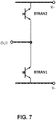
- the circuit of Figure 7 shows a simple circuit configuration for illustration: Suppose that two NPN B-TRAN devices, BTRAN1 and BTRAN2, are connected in series between two supply rails V+ and V- to form a phase leg with an output node OUT. In such a configuration, only one of the B-TRAN devices is allowed to be fully ON at any given instant. Assume that BTRAN1 is connected between the output node and whichever rail is negative (at the moment), and BTRAN2 is connected between the output node and whichever rail is positive (at the moment). Now consider the transition when the phase leg is switched, so that the OUT node is to be pulled up rather than pulled down.
- the pulldown device BTRAN1 will turn off, and the pullup device BTRAN2 will turn on. This means that BTRAN1 will go into reverse recovery.
- the device is prepared for reverse recovery by first shorting the e-base to the emitter for pre-off-1, then the e-base is connected to a voltage negative with respect to the emitter (negative e-base drive) in order to complete the removal of charge carriers from the bulk base region (during phase 4, pre-off-2), then due to turn-on of the other B-TRAN in the phase leg the current reverses in B-TRAN-1, whereupon the emitter changes to collector, and e-base changed to c-base, and that device starts blocking voltage from collector to emitter.
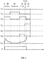
- Figure 1 shows waveform plots for one sample embodiment of turn-off switching using e.g. a base drive circuit like that of Figure 2 .
- the two pre-turnoff timing phases are labeled as " Pre-off 1 " (or phase 2 ) and "Pre-off 2 " (or phase 3 ).
- switch S 21 turns on, briefly driving the e-base negative just before turn-off (which occurs in phase 5 ). This reduces turn-off losses.
- the first timing phase illustrated (phase 0) is the "diode-on" mode.
- switch S 13 is connecting the c-base to the collector. This results in conduction subject to a "diode drop" (about 0.9V for silicon) of forward bias.
- phase 1 The second timing phase illustrated (phase 1) is the "transistor-on" mode.
- switch S 12 is connecting the c-base to a positive voltage with respect to the collector. This results in conduction subject to a very small forward bias (e.g. 200mV or so of V CE ).
- the third timing phase illustrated is the pre-turnoff timing phase "Pre-off 1 " (or phase 2).
- Pre-off 1 the pre-turnoff timing phase
- both of the base contact regions are shorted to their adjacent emitter/collector regions.
- the fourth timing phase illustrated is the second pre-turnoff timing phase "Pre-off 2 " (or phase 3).
- the e-base is driven to reduce conduction; in a PNP device a negative drive is applied to the e-base, as described above.
- phase 4 The last timing phase illustrated is the "active-off' timing phase (phase 4). In this timing phase both of the base contact regions are shorted to their adjacent emitter/collector regions.
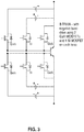
- Figure 3 shows another negative base drive circuit, which operates a B-TRAN (silicon in this example) using two GaN MOSFETs and one Si MOSFET on each base. Since the bandgap of GaN is higher than Si, the larger diode drop voltage (of the body diode) of the GaN MOSFETs provides a differential with respect to the body diodes of the silicon devices.
- B-TRAN silicon in this example
- Figure 4 shows waveform plots for one sample embodiment of reverse recovery switching for a negative base drive like e.g. that of Figure 2 .
- the negative base drive briefly pulls the e-base negative to reduce turn-on and reverse recovery losses.
- Figure 5 shows another negative base drive circuit, which operates a B-TRAN using two Si MOSFET pairs and one Si MOSFET on each base.
- Figure 6 shows an example of a B-TRAN device structure.
- both faces of a semiconductor die carry emitter/collector regions 622 which form a junction with the bulk substrate 610.
- Base contact regions 632 are also present on both faces.
- This example shows an NPN structure, so the emitter/collector regions 622 are n-type, and the base contact regions 632 are p-type.
- a shallow n+ contact doping 624 provides ohmic contact from separate terminals EC1 and EC2 (on the two opposite faces of the semiconductor die, in this example) to regions 622
- a shallow p+ contact doping 634 provides ohmic contact from separate terminals B1 and B2 (on the two opposite faces of the die) to regions 632.
- dielectric-filled trenches 640 provide lateral separation between base contact regions 632 and emitter/collector regions 622. (Note that a p-type diffused region may be added to reduce the series resistance between the emitter-to-base junction and the base contact.) B-TRANs can provide significantly better efficiency than is conventionally available for existing static transfer switches; for example, a 1200V B-TRAN has an expected system efficiency of 99.9%.
- Methods and systems for operating a double-base bidirectional power bipolar transistor Two timing phases are used to transition into turn-off: one where each base is shorted to its nearest emitter/collector region, and a second one where negative drive is applied to the emitter-side base to reduce the minority carrier population in the bulk substrate.
- a diode prevents reverse turn-on while negative base drive is being applied.
- a method for operating a bidirectional bipolar power transistor which has two distinct n-type emitter/collector regions on opposite faces of a p-type semiconductor die, and two distinct p-type base contact regions on the opposite faces of the die, comprising: 1) in a transistor-ON timing phase, when minimal voltage drop is desired, biasing a first one of the base contact regions, which is closest to whichever of the emitter/collector regions is more positive at the moment, to a voltage which causes bipolar conduction, to thereby reduce the voltage drop between the two emitter/collector regions; and thereafter 2) in a first pre-turnoff timing phase, shorting each of the base contact regions to the respectively nearest one of the emitter/collector regions, to thereby increase the voltage drop between the two emitter/collector regions; and thereafter 3) in a second pre-turnoff timing phase, biasing the second base contact regions negative with respect to its nearest emitter/collector region, to thereby reduce the minority carrier concentration in the bulk base region.
- a method for operating a bidirectional bipolar power transistor which has two distinct n-type emitter/collector regions on opposite faces of a p-type semiconductor die, and two distinct p-type base contact regions on the opposite faces of the die, comprising, when a first one of the emitter/collector regions is more positive than a second one of the emitter/collector regions: 0) in a diode-ON timing phase, shorting a first one of the base contact regions to the first emitter/collector region, which is the nearest thereto, to thereby initiate conduction between the two emitter/collector regions; and thereafter 1) in a transistor-ON timing phase, when minimal voltage drop is desired, biasing the first base contact region to a voltage which causes bipolar conduction, to thereby reduce the voltage drop between the two emitter/collector regions; and thereafter 2) in a first pre-turnoff timing phase, shorting each of the base contact regions to the respectively nearest one of the emitter/collector regions, to thereby
- a method for operating a bidirectional bipolar transistor which has two first-conductivity-type emitter/collector regions in distinct locations separated by a bulk second-conductivity-type base region, and two distinct second-conductivity-type base contact regions which connect to the bulk base region in mutually separate locations, comprising: 1) in a transistor-ON timing phase, when minimal voltage drop is desired, biasing a first one of the base contact regions, which is closer than a second one of the base contact regions to whichever of the emitter/collector regions is positioned to act as the collector, as defined by externally applied voltage polarity, to a voltage which causes bipolar conduction to reduce the voltage drop between the two emitter/collector regions; and thereafter 2) in a first pre-turnoff timing phase, shorting each of the base contact regions to the respectively nearest one of the emitter/collector regions; and thereafter 3) in a second pre-turnoff timing phase, biasing the second base contact regions with a polarity opposite to that applied to
- a method for operating a bidirectional bipolar power transistor which has two distinct n-type emitter/collector regions on opposite faces of a p-type semiconductor die, and two distinct p-type base contact regions on the opposite faces of the die, comprising: 1) in a transistor-ON timing phase, when minimal voltage drop is desired, biasing a first one of the base contact regions, which is closest to whichever of the emitter/collector regions is more positive at the moment, to a voltage which causes bipolar conduction, to thereby reduce the voltage drop between the two emitter/collector regions; and thereafter 2) in a first pre-turnoff timing phase, shorting each of the base contact regions to the respectively nearest one of the emitter/collector regions, to thereby increase the voltage drop between the two emitter/collector regions; and thereafter 3) in a second pre-turnoff timing phase, biasing the second base contact regions negative with respect to its nearest emitter/collector region, to thereby reduce the minority carrier concentration in the bulk base region; and
Landscapes
- Engineering & Computer Science (AREA)
- Power Engineering (AREA)
- Bipolar Integrated Circuits (AREA)
- Bipolar Transistors (AREA)
- Power Conversion In General (AREA)
- Electronic Switches (AREA)
Claims (9)
- Procédé de fonctionnement d'un transistor de puissance bipolaire bidirectionnel qui a deux régions distinctes d'émetteur/collecteur de premier type de conductivité (622) sur des faces opposées d'un substrat massif de deuxième type de conductivité (610) d'une puce semi-conductrice, et deux régions distinctes de contact de base de second type de conductivité (632) sur les faces opposées du substrat massif (610), le procédé comprenant de :1) dans une phase de synchronisation de transistor-activé, lorsqu'une chute de tension minimale est souhaitée, polariser une première des régions de contact de base (632), qui est la plus proche de celle des régions d'émetteur/collecteur (622) qui agit comme collecteur,
comme défini par une polarité de tension appliquée extérieurement, à une tension qui provoque une conduction bipolaire, pour ainsi réduire la chute de tension entre les deux régions d'émetteur/collecteur (622) ; puis2) dans une première phase de synchronisation de pré-coupure, court-circuiter chacune des régions de contact de base (632) de la région respectivement la plus proche des régions d'émetteur/collecteur (622), pour ainsi augmenter la chute de tension entre les deux régions d'émetteur/collecteur (622) ; et ensuite caractérisé par3) dans une seconde phase de synchronisation de pré-coupure, polariser la seconde région de contact de base (632) avec une polarité opposée à celle appliquée à la première région de contact de base (632) à l'étape 1), pour ainsi réduire la concentration de porteurs minoritaires dans le substrat massif (610). - Procédé selon la revendication 1, comprenant en outre, avant l'étape 1) de :0) dans une phase de synchronisation de diode-activée, court-circuiter la première des régions de contact de base (632) de sa région d'émetteur/collecteur (622) la plus proche, pour ainsi initier la conduction entre les deux régions d'émetteur/collecteur (622);
et comprenant en outre, après l'étape 3) de :4) court-circuiter la seconde région de contact de base (632) de sa région d'émetteur/collecteur (622) la plus proche, pour maintenir le dispositif désactivé. - Procédé selon la revendication 1, comprenant en outre, après l'étape 3) de :
4) désactiver le dispositif. - Procédé selon la revendication 1, comprenant en outre de :
lors de l'étape 3), utiliser une diode pour bloquer le courant qui aurait tendance à activer la conduction dans un sens opposé à celui de l'étape 1). - Procédé selon l'une quelconque des revendications précédentes, dans lequel le premier type de conductivité est le type n.
- Procédé selon l'une quelconque des revendications 1 à 4, dans lequel l'étape 3) a une durée plus courte que l'étape 2).
- Procédé selon l'une quelconque des revendications 1 à 4, dans lequel la puce semi-conductrice est en silicium.
- Circuit d'attaque de base qui est connecté à un transistor de puissance bipolaire bidirectionnel à double base,
dans lequel le transistor de puissance bipolaire bidirectionnel a deux régions distinctes d'émetteur/collecteur de premier type de conductivité (622) sur des faces opposées d'un substrat massif de deuxième type de conductivité (610) d'une puce semi-conductrice, et deux régions distinctes de contact de base de deuxième type de conductivité (632) sur les faces opposées du substrat massif (610) ;
dans lequel le circuit d'attaque de base comprend trois branches de circuit (S11, S12, S13; S21, S22, S23) connectées à chacune des deux régions de contact de base (632) du transistor de puissance bipolaire bidirectionnel, dans lequel une branche de circuit (S13; S23) peut fonctionner pour fournir une conduction bidirectionnelle, et les autres branches de circuit (S11; S21, S12; S22) peuvent fonctionner pour fournir des décalages de tension de différentes polarités;
et dans lequel le circuit d'attaque de base est configuré pour mettre en œuvre le procédé selon l'une quelconque des revendications 1 à 4. - Circuit d'attaque de base selon la revendication 8, qui comprend en outre une diode à barrière de Schottky qui est connectée pour bloquer l'activation de la conduction inverse pendant des périodes d'attaque de base négative.
Applications Claiming Priority (3)
| Application Number | Priority Date | Filing Date | Title |
|---|---|---|---|
| US201562218978P | 2015-09-15 | 2015-09-15 | |
| US201562239815P | 2015-10-09 | 2015-10-09 | |
| PCT/US2016/052008 WO2017049006A1 (fr) | 2015-09-15 | 2016-09-15 | Fonctionnement de transistors bipolaires à double base avec phases de temporisation supplémentaires au niveau des transitions de commutation |
Publications (3)
| Publication Number | Publication Date |
|---|---|
| EP3350914A1 EP3350914A1 (fr) | 2018-07-25 |
| EP3350914A4 EP3350914A4 (fr) | 2018-08-29 |
| EP3350914B1 true EP3350914B1 (fr) | 2021-04-07 |
Family
ID=58289894
Family Applications (1)
| Application Number | Title | Priority Date | Filing Date |
|---|---|---|---|
| EP16847338.7A Active EP3350914B1 (fr) | 2015-09-15 | 2016-09-15 | Fonctionnement de transistors bipolaires à double base avec phases de temporisation supplémentaires au niveau des transitions de commutation |
Country Status (5)
| Country | Link |
|---|---|
| EP (1) | EP3350914B1 (fr) |
| JP (1) | JP6879572B2 (fr) |
| KR (1) | KR102590999B1 (fr) |
| CN (1) | CN108028603B (fr) |
| WO (1) | WO2017049006A1 (fr) |
Families Citing this family (4)
| Publication number | Priority date | Publication date | Assignee | Title |
|---|---|---|---|---|
| JP2019067796A (ja) * | 2017-09-28 | 2019-04-25 | ルネサスエレクトロニクス株式会社 | 半導体装置およびその製造方法 |
| US11411557B2 (en) * | 2020-05-18 | 2022-08-09 | Ideal Power Inc. | Method and system of operating a bi-directional double-base bipolar junction transistor (B-TRAN) |
| JP7605320B2 (ja) * | 2020-12-10 | 2024-12-24 | アイディール パワー インコーポレイテッド | 双方向ダブルベースバイポーラ接合トランジスタ(b-tran)を動作させる方法及びシステム |
| WO2023018769A1 (fr) * | 2021-08-10 | 2023-02-16 | Ideal Power Inc. | Système et procédé pour commutateurs de puissance à tranchée bidirectionnelle |
Family Cites Families (13)
| Publication number | Priority date | Publication date | Assignee | Title |
|---|---|---|---|---|
| JP3142057B2 (ja) * | 1997-11-13 | 2001-03-07 | 日本電気株式会社 | 半導体装置とその製造方法、及び駆動装置 |
| ES2250171T3 (es) * | 1999-10-14 | 2006-04-16 | Alcatel | Disposicion de conmutacion con transistor bipolar bidireccional. |
| JP4065825B2 (ja) * | 2002-12-10 | 2008-03-26 | シャープ株式会社 | 双方向フォトサイリスタチップ、光点弧カプラ、および、ソリッドステートリレー |
| JP2005051852A (ja) * | 2003-07-30 | 2005-02-24 | Sanyo Electric Co Ltd | モータ駆動回路、集積回路、モータ回路の駆動方法 |
| US7663898B2 (en) * | 2004-06-07 | 2010-02-16 | Ixys Corporation | Switching power supply with direct conversion off AC power source |
| JP2008300590A (ja) * | 2007-05-31 | 2008-12-11 | Fuji Electric Device Technology Co Ltd | 双方向横形絶縁ゲート型バイポーラトランジスタ |
| US8294507B2 (en) * | 2009-05-08 | 2012-10-23 | Cree, Inc. | Wide bandgap bipolar turn-off thyristor having non-negative temperature coefficient and related control circuits |
| US8681518B2 (en) * | 2009-07-21 | 2014-03-25 | Cree, Inc. | High speed rectifier circuit |
| KR101922397B1 (ko) * | 2011-05-20 | 2018-11-28 | 가부시키가이샤 한도오따이 에네루기 켄큐쇼 | 반도체 장치 |
| US9356536B2 (en) * | 2013-01-11 | 2016-05-31 | ABBI Research Ltd. | Bidirectional power conversion with fault-handling capability |
| US9685502B2 (en) * | 2013-02-07 | 2017-06-20 | John Wood | Bipolar junction transistor structure |
| GB2524699C (en) * | 2013-02-07 | 2018-11-14 | Wood John | A bipolar junction transistor structure |
| EP3116028B1 (fr) * | 2013-06-24 | 2021-03-24 | Ideal Power Inc. | Systèmes, circuits, dispositifs et procédés utilisant des transistors bipolaires bidirectionnels |
-
2016
- 2016-09-15 EP EP16847338.7A patent/EP3350914B1/fr active Active
- 2016-09-15 CN CN201680052122.2A patent/CN108028603B/zh active Active
- 2016-09-15 WO PCT/US2016/052008 patent/WO2017049006A1/fr not_active Ceased
- 2016-09-15 JP JP2018513600A patent/JP6879572B2/ja active Active
- 2016-09-15 KR KR1020187002332A patent/KR102590999B1/ko active Active
Non-Patent Citations (1)
| Title |
|---|
| None * |
Also Published As
| Publication number | Publication date |
|---|---|
| EP3350914A4 (fr) | 2018-08-29 |
| KR20180042230A (ko) | 2018-04-25 |
| CN108028603A (zh) | 2018-05-11 |
| WO2017049006A1 (fr) | 2017-03-23 |
| KR102590999B1 (ko) | 2023-10-18 |
| JP6879572B2 (ja) | 2021-06-02 |
| JP2018533205A (ja) | 2018-11-08 |
| CN108028603B (zh) | 2020-04-24 |
| EP3350914A1 (fr) | 2018-07-25 |
Similar Documents
| Publication | Publication Date | Title |
|---|---|---|
| US10211283B2 (en) | Operation of double-base bipolar transistors with additional timing phases at switching transitions | |
| US9742395B2 (en) | Circuits, methods, and systems with optimized operation of double-base bipolar junction transistors | |
| US11721689B2 (en) | Semiconductor device having a semiconductor channel region and a semiconductor auxiliary region | |
| US10497699B2 (en) | Double-base-connected bipolar transistors with passive components preventing accidental turn-on | |
| US9742385B2 (en) | Bidirectional semiconductor switch with passive turnoff | |
| EP2901483B1 (fr) | Systèmes, circuits, dispositifs et procédés avec transistors bipolaires bidirectionnels | |
| US9787304B2 (en) | Methods, systems, and devices for active charge control diodes | |
| EP3350914B1 (fr) | Fonctionnement de transistors bipolaires à double base avec phases de temporisation supplémentaires au niveau des transitions de commutation |
Legal Events
| Date | Code | Title | Description |
|---|---|---|---|
| STAA | Information on the status of an ep patent application or granted ep patent |
Free format text: STATUS: THE INTERNATIONAL PUBLICATION HAS BEEN MADE |
|
| PUAI | Public reference made under article 153(3) epc to a published international application that has entered the european phase |
Free format text: ORIGINAL CODE: 0009012 |
|
| STAA | Information on the status of an ep patent application or granted ep patent |
Free format text: STATUS: REQUEST FOR EXAMINATION WAS MADE |
|
| 17P | Request for examination filed |
Effective date: 20180314 |
|
| AK | Designated contracting states |
Kind code of ref document: A1 Designated state(s): AL AT BE BG CH CY CZ DE DK EE ES FI FR GB GR HR HU IE IS IT LI LT LU LV MC MK MT NL NO PL PT RO RS SE SI SK SM TR |
|
| AX | Request for extension of the european patent |
Extension state: BA ME |
|
| A4 | Supplementary search report drawn up and despatched |
Effective date: 20180730 |
|
| RIC1 | Information provided on ipc code assigned before grant |
Ipc: H01L 29/747 20060101ALI20180724BHEP Ipc: H02M 3/158 20060101AFI20180724BHEP Ipc: H03K 17/60 20060101ALI20180724BHEP Ipc: H03K 17/567 20060101ALN20180724BHEP Ipc: H03K 17/0412 20060101ALN20180724BHEP |
|
| DAV | Request for validation of the european patent (deleted) | ||
| DAX | Request for extension of the european patent (deleted) | ||
| GRAP | Despatch of communication of intention to grant a patent |
Free format text: ORIGINAL CODE: EPIDOSNIGR1 |
|
| STAA | Information on the status of an ep patent application or granted ep patent |
Free format text: STATUS: GRANT OF PATENT IS INTENDED |
|
| RIC1 | Information provided on ipc code assigned before grant |
Ipc: H02M 3/158 20060101AFI20200930BHEP Ipc: H03K 17/60 20060101ALI20200930BHEP Ipc: H01L 29/732 20060101ALI20200930BHEP Ipc: H01L 29/747 20060101ALI20200930BHEP Ipc: H03K 17/567 20060101ALN20200930BHEP Ipc: H01L 29/10 20060101ALI20200930BHEP Ipc: H03K 17/0412 20060101ALN20200930BHEP Ipc: H01L 29/66 20060101ALI20200930BHEP |
|
| INTG | Intention to grant announced |
Effective date: 20201023 |
|
| GRAJ | Information related to disapproval of communication of intention to grant by the applicant or resumption of examination proceedings by the epo deleted |
Free format text: ORIGINAL CODE: EPIDOSDIGR1 |
|
| STAA | Information on the status of an ep patent application or granted ep patent |
Free format text: STATUS: REQUEST FOR EXAMINATION WAS MADE |
|
| GRAP | Despatch of communication of intention to grant a patent |
Free format text: ORIGINAL CODE: EPIDOSNIGR1 |
|
| STAA | Information on the status of an ep patent application or granted ep patent |
Free format text: STATUS: GRANT OF PATENT IS INTENDED |
|
| INTC | Intention to grant announced (deleted) | ||
| RIC1 | Information provided on ipc code assigned before grant |
Ipc: H03K 17/567 20060101ALN20210119BHEP Ipc: H03K 17/60 20060101ALI20210119BHEP Ipc: H01L 29/10 20060101ALI20210119BHEP Ipc: H03K 17/0412 20060101ALN20210119BHEP Ipc: H01L 29/747 20060101ALI20210119BHEP Ipc: H02M 3/158 20060101AFI20210119BHEP Ipc: H01L 29/732 20060101ALI20210119BHEP Ipc: H01L 29/66 20060101ALI20210119BHEP |
|
| GRAS | Grant fee paid |
Free format text: ORIGINAL CODE: EPIDOSNIGR3 |
|
| GRAA | (expected) grant |
Free format text: ORIGINAL CODE: 0009210 |
|
| STAA | Information on the status of an ep patent application or granted ep patent |
Free format text: STATUS: THE PATENT HAS BEEN GRANTED |
|
| INTG | Intention to grant announced |
Effective date: 20210216 |
|
| AK | Designated contracting states |
Kind code of ref document: B1 Designated state(s): AL AT BE BG CH CY CZ DE DK EE ES FI FR GB GR HR HU IE IS IT LI LT LU LV MC MK MT NL NO PL PT RO RS SE SI SK SM TR |
|
| REG | Reference to a national code |
Ref country code: GB Ref legal event code: FG4D |
|
| REG | Reference to a national code |
Ref country code: CH Ref legal event code: EP Ref country code: CH Ref legal event code: NV Representative=s name: SERVOPATENT GMBH, CH Ref country code: AT Ref legal event code: REF Ref document number: 1380969 Country of ref document: AT Kind code of ref document: T Effective date: 20210415 |
|
| REG | Reference to a national code |
Ref country code: DE Ref legal event code: R096 Ref document number: 602016055826 Country of ref document: DE |
|
| REG | Reference to a national code |
Ref country code: IE Ref legal event code: FG4D |
|
| REG | Reference to a national code |
Ref country code: NL Ref legal event code: FP |
|
| REG | Reference to a national code |
Ref country code: LT Ref legal event code: MG9D |
|
| REG | Reference to a national code |
Ref country code: AT Ref legal event code: MK05 Ref document number: 1380969 Country of ref document: AT Kind code of ref document: T Effective date: 20210407 |
|
| PG25 | Lapsed in a contracting state [announced via postgrant information from national office to epo] |
Ref country code: FI Free format text: LAPSE BECAUSE OF FAILURE TO SUBMIT A TRANSLATION OF THE DESCRIPTION OR TO PAY THE FEE WITHIN THE PRESCRIBED TIME-LIMIT Effective date: 20210407 Ref country code: LT Free format text: LAPSE BECAUSE OF FAILURE TO SUBMIT A TRANSLATION OF THE DESCRIPTION OR TO PAY THE FEE WITHIN THE PRESCRIBED TIME-LIMIT Effective date: 20210407 Ref country code: AT Free format text: LAPSE BECAUSE OF FAILURE TO SUBMIT A TRANSLATION OF THE DESCRIPTION OR TO PAY THE FEE WITHIN THE PRESCRIBED TIME-LIMIT Effective date: 20210407 Ref country code: BG Free format text: LAPSE BECAUSE OF FAILURE TO SUBMIT A TRANSLATION OF THE DESCRIPTION OR TO PAY THE FEE WITHIN THE PRESCRIBED TIME-LIMIT Effective date: 20210707 Ref country code: HR Free format text: LAPSE BECAUSE OF FAILURE TO SUBMIT A TRANSLATION OF THE DESCRIPTION OR TO PAY THE FEE WITHIN THE PRESCRIBED TIME-LIMIT Effective date: 20210407 |
|
| PG25 | Lapsed in a contracting state [announced via postgrant information from national office to epo] |
Ref country code: NO Free format text: LAPSE BECAUSE OF FAILURE TO SUBMIT A TRANSLATION OF THE DESCRIPTION OR TO PAY THE FEE WITHIN THE PRESCRIBED TIME-LIMIT Effective date: 20210707 Ref country code: PT Free format text: LAPSE BECAUSE OF FAILURE TO SUBMIT A TRANSLATION OF THE DESCRIPTION OR TO PAY THE FEE WITHIN THE PRESCRIBED TIME-LIMIT Effective date: 20210809 Ref country code: PL Free format text: LAPSE BECAUSE OF FAILURE TO SUBMIT A TRANSLATION OF THE DESCRIPTION OR TO PAY THE FEE WITHIN THE PRESCRIBED TIME-LIMIT Effective date: 20210407 Ref country code: RS Free format text: LAPSE BECAUSE OF FAILURE TO SUBMIT A TRANSLATION OF THE DESCRIPTION OR TO PAY THE FEE WITHIN THE PRESCRIBED TIME-LIMIT Effective date: 20210407 Ref country code: SE Free format text: LAPSE BECAUSE OF FAILURE TO SUBMIT A TRANSLATION OF THE DESCRIPTION OR TO PAY THE FEE WITHIN THE PRESCRIBED TIME-LIMIT Effective date: 20210407 Ref country code: GR Free format text: LAPSE BECAUSE OF FAILURE TO SUBMIT A TRANSLATION OF THE DESCRIPTION OR TO PAY THE FEE WITHIN THE PRESCRIBED TIME-LIMIT Effective date: 20210708 Ref country code: LV Free format text: LAPSE BECAUSE OF FAILURE TO SUBMIT A TRANSLATION OF THE DESCRIPTION OR TO PAY THE FEE WITHIN THE PRESCRIBED TIME-LIMIT Effective date: 20210407 Ref country code: IS Free format text: LAPSE BECAUSE OF FAILURE TO SUBMIT A TRANSLATION OF THE DESCRIPTION OR TO PAY THE FEE WITHIN THE PRESCRIBED TIME-LIMIT Effective date: 20210807 |
|
| REG | Reference to a national code |
Ref country code: DE Ref legal event code: R097 Ref document number: 602016055826 Country of ref document: DE |
|
| PG25 | Lapsed in a contracting state [announced via postgrant information from national office to epo] |
Ref country code: DK Free format text: LAPSE BECAUSE OF FAILURE TO SUBMIT A TRANSLATION OF THE DESCRIPTION OR TO PAY THE FEE WITHIN THE PRESCRIBED TIME-LIMIT Effective date: 20210407 Ref country code: CZ Free format text: LAPSE BECAUSE OF FAILURE TO SUBMIT A TRANSLATION OF THE DESCRIPTION OR TO PAY THE FEE WITHIN THE PRESCRIBED TIME-LIMIT Effective date: 20210407 Ref country code: EE Free format text: LAPSE BECAUSE OF FAILURE TO SUBMIT A TRANSLATION OF THE DESCRIPTION OR TO PAY THE FEE WITHIN THE PRESCRIBED TIME-LIMIT Effective date: 20210407 Ref country code: ES Free format text: LAPSE BECAUSE OF FAILURE TO SUBMIT A TRANSLATION OF THE DESCRIPTION OR TO PAY THE FEE WITHIN THE PRESCRIBED TIME-LIMIT Effective date: 20210407 Ref country code: RO Free format text: LAPSE BECAUSE OF FAILURE TO SUBMIT A TRANSLATION OF THE DESCRIPTION OR TO PAY THE FEE WITHIN THE PRESCRIBED TIME-LIMIT Effective date: 20210407 Ref country code: SM Free format text: LAPSE BECAUSE OF FAILURE TO SUBMIT A TRANSLATION OF THE DESCRIPTION OR TO PAY THE FEE WITHIN THE PRESCRIBED TIME-LIMIT Effective date: 20210407 Ref country code: SK Free format text: LAPSE BECAUSE OF FAILURE TO SUBMIT A TRANSLATION OF THE DESCRIPTION OR TO PAY THE FEE WITHIN THE PRESCRIBED TIME-LIMIT Effective date: 20210407 |
|
| PLBE | No opposition filed within time limit |
Free format text: ORIGINAL CODE: 0009261 |
|
| STAA | Information on the status of an ep patent application or granted ep patent |
Free format text: STATUS: NO OPPOSITION FILED WITHIN TIME LIMIT |
|
| 26N | No opposition filed |
Effective date: 20220110 |
|
| REG | Reference to a national code |
Ref country code: BE Ref legal event code: MM Effective date: 20210930 |
|
| PG25 | Lapsed in a contracting state [announced via postgrant information from national office to epo] |
Ref country code: IS Free format text: LAPSE BECAUSE OF FAILURE TO SUBMIT A TRANSLATION OF THE DESCRIPTION OR TO PAY THE FEE WITHIN THE PRESCRIBED TIME-LIMIT Effective date: 20210807 Ref country code: MC Free format text: LAPSE BECAUSE OF FAILURE TO SUBMIT A TRANSLATION OF THE DESCRIPTION OR TO PAY THE FEE WITHIN THE PRESCRIBED TIME-LIMIT Effective date: 20210407 Ref country code: AL Free format text: LAPSE BECAUSE OF FAILURE TO SUBMIT A TRANSLATION OF THE DESCRIPTION OR TO PAY THE FEE WITHIN THE PRESCRIBED TIME-LIMIT Effective date: 20210407 |
|
| PG25 | Lapsed in a contracting state [announced via postgrant information from national office to epo] |
Ref country code: LU Free format text: LAPSE BECAUSE OF NON-PAYMENT OF DUE FEES Effective date: 20210915 Ref country code: IE Free format text: LAPSE BECAUSE OF NON-PAYMENT OF DUE FEES Effective date: 20210915 Ref country code: BE Free format text: LAPSE BECAUSE OF NON-PAYMENT OF DUE FEES Effective date: 20210930 |
|
| PG25 | Lapsed in a contracting state [announced via postgrant information from national office to epo] |
Ref country code: HU Free format text: LAPSE BECAUSE OF FAILURE TO SUBMIT A TRANSLATION OF THE DESCRIPTION OR TO PAY THE FEE WITHIN THE PRESCRIBED TIME-LIMIT; INVALID AB INITIO Effective date: 20160915 |
|
| P01 | Opt-out of the competence of the unified patent court (upc) registered |
Effective date: 20230515 |
|
| PG25 | Lapsed in a contracting state [announced via postgrant information from national office to epo] |
Ref country code: CY Free format text: LAPSE BECAUSE OF FAILURE TO SUBMIT A TRANSLATION OF THE DESCRIPTION OR TO PAY THE FEE WITHIN THE PRESCRIBED TIME-LIMIT Effective date: 20210407 |
|
| PG25 | Lapsed in a contracting state [announced via postgrant information from national office to epo] |
Ref country code: MK Free format text: LAPSE BECAUSE OF FAILURE TO SUBMIT A TRANSLATION OF THE DESCRIPTION OR TO PAY THE FEE WITHIN THE PRESCRIBED TIME-LIMIT Effective date: 20210407 |
|
| PG25 | Lapsed in a contracting state [announced via postgrant information from national office to epo] |
Ref country code: MT Free format text: LAPSE BECAUSE OF FAILURE TO SUBMIT A TRANSLATION OF THE DESCRIPTION OR TO PAY THE FEE WITHIN THE PRESCRIBED TIME-LIMIT Effective date: 20210407 |
|
| REG | Reference to a national code |
Ref country code: CH Ref legal event code: U11 Free format text: ST27 STATUS EVENT CODE: U-0-0-U10-U11 (AS PROVIDED BY THE NATIONAL OFFICE) Effective date: 20251001 |
|
| PGFP | Annual fee paid to national office [announced via postgrant information from national office to epo] |
Ref country code: DE Payment date: 20250929 Year of fee payment: 10 |
|
| PGFP | Annual fee paid to national office [announced via postgrant information from national office to epo] |
Ref country code: NL Payment date: 20250926 Year of fee payment: 10 Ref country code: IT Payment date: 20250919 Year of fee payment: 10 |
|
| PGFP | Annual fee paid to national office [announced via postgrant information from national office to epo] |
Ref country code: GB Payment date: 20250929 Year of fee payment: 10 |
|
| PGFP | Annual fee paid to national office [announced via postgrant information from national office to epo] |
Ref country code: FR Payment date: 20250925 Year of fee payment: 10 |
|
| PG25 | Lapsed in a contracting state [announced via postgrant information from national office to epo] |
Ref country code: TR Free format text: LAPSE BECAUSE OF FAILURE TO SUBMIT A TRANSLATION OF THE DESCRIPTION OR TO PAY THE FEE WITHIN THE PRESCRIBED TIME-LIMIT Effective date: 20210407 |
|
| PGFP | Annual fee paid to national office [announced via postgrant information from national office to epo] |
Ref country code: CH Payment date: 20251001 Year of fee payment: 10 |