EP3351983B1 - Procédé et système de coupleurs à réseau incorporant des guides d'onde perturbés - Google Patents
Procédé et système de coupleurs à réseau incorporant des guides d'onde perturbés Download PDFInfo
- Publication number
- EP3351983B1 EP3351983B1 EP18157074.8A EP18157074A EP3351983B1 EP 3351983 B1 EP3351983 B1 EP 3351983B1 EP 18157074 A EP18157074 A EP 18157074A EP 3351983 B1 EP3351983 B1 EP 3351983B1
- Authority
- EP
- European Patent Office
- Prior art keywords
- grating coupler
- optical
- waveguides
- grating
- perturbed
- Prior art date
- Legal status (The legal status is an assumption and is not a legal conclusion. Google has not performed a legal analysis and makes no representation as to the accuracy of the status listed.)
- Active
Links
Images


Classifications
-
- G—PHYSICS
- G02—OPTICS
- G02B—OPTICAL ELEMENTS, SYSTEMS OR APPARATUS
- G02B6/00—Light guides; Structural details of arrangements comprising light guides and other optical elements, e.g. couplings
- G02B6/24—Coupling light guides
- G02B6/26—Optical coupling means
-
- G—PHYSICS
- G02—OPTICS
- G02B—OPTICAL ELEMENTS, SYSTEMS OR APPARATUS
- G02B6/00—Light guides; Structural details of arrangements comprising light guides and other optical elements, e.g. couplings
- G02B6/24—Coupling light guides
- G02B6/26—Optical coupling means
- G02B6/34—Optical coupling means utilising prism or grating
-
- G—PHYSICS
- G02—OPTICS
- G02B—OPTICAL ELEMENTS, SYSTEMS OR APPARATUS
- G02B5/00—Optical elements other than lenses
- G02B5/18—Diffraction gratings
- G02B5/1861—Reflection gratings characterised by their structure, e.g. step profile, contours of substrate or grooves, pitch variations, materials
-
- G—PHYSICS
- G02—OPTICS
- G02B—OPTICAL ELEMENTS, SYSTEMS OR APPARATUS
- G02B6/00—Light guides; Structural details of arrangements comprising light guides and other optical elements, e.g. couplings
- G02B6/10—Light guides; Structural details of arrangements comprising light guides and other optical elements, e.g. couplings of the optical waveguide type
- G02B6/12—Light guides; Structural details of arrangements comprising light guides and other optical elements, e.g. couplings of the optical waveguide type of the integrated circuit kind
- G02B6/122—Basic optical elements, e.g. light-guiding paths
- G02B6/124—Geodesic lenses or integrated gratings
-
- G—PHYSICS
- G02—OPTICS
- G02B—OPTICAL ELEMENTS, SYSTEMS OR APPARATUS
- G02B6/00—Light guides; Structural details of arrangements comprising light guides and other optical elements, e.g. couplings
- G02B6/24—Coupling light guides
- G02B6/26—Optical coupling means
- G02B6/30—Optical coupling means for use between fibre and thin-film device
-
- G—PHYSICS
- G02—OPTICS
- G02B—OPTICAL ELEMENTS, SYSTEMS OR APPARATUS
- G02B6/00—Light guides; Structural details of arrangements comprising light guides and other optical elements, e.g. couplings
- G02B6/10—Light guides; Structural details of arrangements comprising light guides and other optical elements, e.g. couplings of the optical waveguide type
- G02B6/12—Light guides; Structural details of arrangements comprising light guides and other optical elements, e.g. couplings of the optical waveguide type of the integrated circuit kind
- G02B2006/12083—Constructional arrangements
- G02B2006/12107—Grating
Definitions
- Certain embodiments of the invention relate to semiconductor processing. More specifically, certain embodiments of the invention relate to a method and system for grating couplers incorporating perturbed waveguides.
- US 2006/117178 A1 teaches a distributed optical structure comprising a set of diffractive elements. Individual diffractive element transfer functions collectively yield an overall transfer function between entrance and exit ports. Diffractive elements are defined relative to virtual contours and include diffracting region(s) altered to diffract, reflect, and/or scatter incident optical fields. Optical elements may be configured: as planar or channel waveguides, with curvilinear diffracting segments; to support three-dimensional propagation with surface areal diffracting segments; as a diffraction grating, with grating groove or line segments
- a coupler-multiplexer permutation switch as shown in US 2004/ 208447 A1 integrates multiplexing and switching functions on a single substrate. It has a single-mode/multi-mode backward coupler followed by a digital optical switch (DOS).
- DOS digital optical switch
- the single-mode waveguide channels are phase-matched through a grating with the corresponding, backward-propagating modes of a multi-mode waveguide. The different modes are subsequently separated in a digital optical switch. Different permutations are obtained by electronically controlling an effective-index distribution of DOS output waveguides.
- US 2010/006784 A1 discloses a method and a system for a light source assembly supporting direct coupling to a photonically enabled complementary metal-oxide semiconductor (CMOS) chip.
- the assembly includes include a laser, a microlens, a turning mirror, reciprocal and/or non-reciprocal polarization rotators, and an optical bench.
- the laser generates an optical signal that is focused utilizing the microlens.
- the optical signal is reflected at an angle defined by the turning mirror, and is transmitted out of the light source assembly to one or more grating couplers in the chip.
- the method of the present invention is defined in the appendant clam 1 and the system of the present invention is defined in the appendant claim 2. Further improvements are subject to the dependent claims.
- Certain aspects of the invention may be found in a method and system for grating couplers incorporating perturbed waveguides.
- Exemplary aspects of the invention may comprise in a semiconductor photonics die, communicating optical signals into and/or out of the semiconductor die utilizing a grating coupler on the semiconductor photonics die, where the grating coupler comprises perturbed waveguides.
- the perturbed waveguides may comprise a variable width along a length of the perturbed waveguides.
- the grating coupler may comprise a single polarization grating coupler comprising perturbed waveguides and a non-perturbed grating.
- the grating coupler may comprise a polarization splitting grating coupler that includes two sets of perturbed waveguides at a non-zero angle from each other.
- the polarization splitting grating coupler may comprise discrete scatterers at an intersection of the sets of perturbed waveguides not forming part of the present invention.
- the polarization splitting grating coupler may comprise a plurality of non-linear rows of discrete shapes.
- the grating couplers may be etched in a silicon layer on the semiconductor photonics die or deposited on the semiconductor photonics die.
- the grating coupler may comprise individual scatterers between the perturbed waveguides.
- FIG. 1A is a block diagram of a photonically enabled CMOS chip comprising grating couplers with perturbed waveguides.
- optoelectronic devices on a CMOS chip 130 comprising optical modulators 105A-105D, photodiodes 111A-111D, monitor photodiodes 113A-113H, and optical devices comprising taps 103A-103K, optical terminations 115A-115D, and grating couplers 117A-117H.
- electrical devices and circuits comprising amplifiers 107A-107D, analog and digital control circuits 109, and control sections 112A-112D.
- the amplifiers 107A-107D may comprise transimpedance and limiting amplifiers (TIA/LAs), for example.
- Optical signals are communicated between optical and optoelectronic devices via optical waveguides 110 fabricated in the CMOS chip 130.
- Single-mode or multi-mode waveguides may be used in photonic integrated circuits. Single-mode operation enables direct connection to optical signal processing and networking elements.
- the term "single-mode” may be used for waveguides that support a single mode for each of the two polarizations, transverse-electric (TE) and transverse-magnetic (TM), or for waveguides that are truly single mode and only support one mode whose polarization is TE, which comprises an electric field parallel to the substrate supporting the waveguides.
- Two typical waveguide cross-sections that are utilized comprise strip waveguides and rib waveguides. Strip waveguides typically comprise a rectangular cross-section, whereas rib waveguides comprise a rib section on top of a waveguide slab.
- the optical modulators 105A-105D comprise Mach-Zehnder or ring modulators, for example, and enable the modulation of the continuous-wave (CW) laser input signal.
- the optical modulators 105A-105D comprise high-speed and low-speed phase modulation sections and are controlled by the control sections 112A-112D.
- the high-speed phase modulation section of the optical modulators 105A-105D may modulate a CW light source signal with a data signal.
- the low-speed phase modulation section of the optical modulators 105A-105D may compensate for slowly varying phase factors such as those induced by mismatch between the waveguides, waveguide temperature, or waveguide stress and is referred to as the passive phase, or the passive biasing of the MZI.
- the phase modulators may have a dual role: to compensate for the passive biasing of the MZI and to apply the additional phase modulation used to modulate the light intensity at the output port of the MZI according to a data stream.
- the former phase tuning and the latter phase modulation may be applied by separate, specialized devices, since the former is a low speed, slowly varying contribution, while the latter is typically a high speed signal. These devices are then respectively referred to as the LSPM and the HSPM.
- LSPM thermal phase modulators
- PINPM forward biased PIN junction phase modulators
- An example of an HSPM is a reversed biased PIN junction, where the index of refraction is also modulated via the carrier density, but which allows much faster operation, albeit at a lower phase modulation efficiency per waveguide length.
- the outputs of the modulators 105A-105D may be optically coupled via the waveguides 110 to the grating couplers 117E-117H.
- the taps 103D-103K comprise four-port optical couplers, for example, and are utilized to sample the optical signals generated by the optical modulators 105A-105D, with the sampled signals being measured by the monitor photodiodes 113A-113H.
- the unused branches of the taps 103D-103K are terminated by optical terminations 115A-115D to avoid back reflections of unwanted signals.
- the grating couplers 117A-117H comprise optical gratings that enable coupling of light into and out of the CMOS chip 130.
- the grating couplers 117A-117D may be utilized to couple light received from optical fibers into the CMOS chip 130, and the grating couplers 117E-117H may be utilized to couple light from the CMOS chip 130 into optical fibers.
- the grating couplers 117A-117H may comprise single polarization grating couplers (SPGC) and/or polarization splitting grating couplers (PSGC). In instances where a PSGC is utilized, two input, or output, waveguides may be utilized.
- SPGC single polarization grating couplers
- PSGC polarization splitting grating couplers
- the grating couplers 117A-117H may comprise perturbed waveguides, such that at least one parameter of the structure is altered along the length of the waveguides.
- the width and/or thickness may vary across the length, either in a periodic or aperiodic fashion.
- An aperiodic variation may be useful where more scattering is required in one section of the waveguides as opposed to another, such as in a single polarization grating coupler, where too much scattering at the front section causes the optical mode to have less overlap with an optical fiber centered on the coupler.
- Perturbed waveguides may improve coupling efficiency by enabling the configuring of the optical mode to approximately match that of the optical fiber, i.e., an optical mode from the optical fiber is very similar to the scattered mode in the grating couplers 117A-117H.
- an optical signal may be transmitted out of the CMOS chip 130 by the grating couplers 117A-117H such that the optical mode transmitted is centered on the optical fiber.
- the optical fibers may be epoxied, for example, to the CMOS chip, and may be aligned at an angle from normal to the surface of the CMOS chip 130 to optimize coupling efficiency.
- the optical fibers may comprise single-mode fiber (SMF) and/or polarization-maintaining fiber (PMF).
- Optical signals may be communicated directly into the surface of the CMOS chip 130 without optical fibers by directing a light source on an optical coupling device in the chip, such as the light source interface 135 and/or the optical fiber interface 139. This may be accomplished with directed laser sources and/or optical sources on another chip flip-chip bonded to the CMOS chip 130.
- the photodiodes 111A-111D may convert optical signals received from the grating couplers 117A-117D into electrical signals that are communicated to the amplifiers 107A-107D for processing.
- the photodiodes 111A-111D may comprise high-speed heterojunction phototransistors, for example, and may comprise germanium (Ge) in the collector and base regions for absorption in the 1.3-1.6 ⁇ m optical wavelength range, and may be integrated on a CMOS silicon-on-insulator (SOI) wafer.
- the analog and digital control circuits 109 may control gain levels or other parameters in the operation of the amplifiers 107A-107D, which may then communicate electrical signals off the CMOS chip 130.
- the control sections 112A-112D comprise electronic circuitry that enable modulation of the CW laser signal received from the splitters 103A-103C.
- the optical modulators 105A-105D may require high-speed electrical signals to modulate the refractive index in respective branches of a Mach-Zehnder interferometer (MZI), for example.
- MZI Mach-Zehnder interferometer
- the control sections 112A-112D may include sink and/or source driver electronics that may enable a bidirectional link utilizing a single laser.
- the CMOS chip 130 may be operable to transmit and/or receive and process optical signals.
- Optical signals may be received from optical fibers by the grating couplers 117A-117D and converted to electrical signals by the photodetectors 111A-111D.
- the electrical signals may be amplified by transimpedance amplifiers in the amplifiers 107A-107D, for example, and subsequently communicated to other electronic circuitry, not shown, in the CMOS chip 130.
- CMOS chip 130 Integrated photonics platforms allow the full functionality of an optical transceiver to be integrated on a single chip, the CMOS chip 130, for example.
- a transceiver chip comprises optoelectronic circuits that create and process the optical/electrical signals on the transmitter (Tx) and the receiver (Rx) sides, as well as optical interfaces that couple the optical signal to and from one or more fibers.
- the signal processing functionality may comprise modulating the optical carrier, detecting the optical signal, splitting or combining data streams, and multiplexing or demultiplexing data on carriers with different wavelengths.
- the light source may be external to the chip or may be integrated with the chip in a hybrid scheme. It is often advantageous to have an external continuous-wave (CW) light source, because this architecture allows heat sinking and temperature control of the source separately from the transceiver chip 130.
- An external light source may also be connected to the transceiver chip 130 via a fiber interface.
- An integrated transceiver may comprise at least three optical interfaces, including a transmitter input port to interface to the CW light source, labeled as CW Laser In 101; a transmitter output port to interface to the fiber carrying the optical signal, labeled Optical Signals Out; and a receiver input port to interface to the fiber carrying the optical signal, labeled Optical Signals In.
- Each of the interfaces may comprise grating couplers with perturbed waveguides for reduced optical losses due to reduced mode-mismatch between the fibers and the grating couplers.
- FIG. 1B is a diagram illustrating an exemplary CMOS chip.
- the CMOS chip 130 comprising electronic devices/circuits 131, optical and optoelectronic devices 133, a light source interface 135, CMOS chip front surface 137, an optical fiber interface 139, and CMOS guard ring 141.
- the light source interface 135 and the optical fiber interface 139 comprise grating couplers, for example, that enable coupling of light signals via the CMOS chip surface 137, as opposed to the edges of the chip as with conventional edge-emitting devices. Coupling light signals via the CMOS chip surface 137 enables the use of the CMOS guard ring 141 which protects the chip mechanically and prevents the entry of contaminants via the chip edge.
- the grating couplers may comprise perturbed waveguides for reduced optical mode mismatch between the grating coupler and an optical source, such as an optical fiber.
- the electronic devices/circuits 131 comprise circuitry such as the amplifiers 107A-107D and the analog and digital control circuits 109 described with respect to FIG. 1A , for example.
- the optical and optoelectronic devices 133 comprise devices such as the taps 103A-103K, optical terminations 115A-115D, grating couplers 117A-117H, optical modulators 105A-105D, high-speed heterojunction photodiodes 111A-111D, and monitor photodiodes 113A-113H.
- FIG. 1C is a diagram illustrating a CMOS chip coupled to an optical fiber cable.
- the CMOS chip 130 comprising the CMOS chip surface 137, and the CMOS guard ring 141.
- a fiber-to-chip coupler 143 there is also shown a fiber-to-chip coupler 143, an optical fiber cable 145, and an optical source assembly 147.
- the CMOS chip 130 comprising the electronic devices/circuits 131, the optical and optoelectronic devices 133, the light source interface 135, the CMOS chip surface 137, and the CMOS guard ring 141 may be as described with respect to FIG. 1B .
- the optical fiber cable may be affixed, via epoxy for example, to the CMOS chip surface 137.
- the fiber chip coupler 143 enables the physical coupling of the optical fiber cable 145 to the CMOS chip 130.
- the light source interface 135 and the optical fiber interface 139 comprise grating couplers shown in FIG. 1B may comprise perturbed waveguides for reduced optical mode mismatch between the grating couplers and the optical fiber cable 145 and the light source module 147.
- FIG. 2 is a schematic illustrating an optical transceiver including a photonic interposer comprising grating couplers with perturbed waveguides.
- a photonic transceiver 200 comprising a printed circuit board (PCB)/substrate 201, a silicon photonic interposer 203, an electronic CMOS die 205, through silicon vias (TSVs) 206, copper pillars 207, an optical source module 209, an optical input/output (I/O) 211, wire bonds 213, optical epoxy 215, and optical fibers 217.
- PCB printed circuit board
- TSVs silicon vias
- I/O optical input/output
- the PCB/substrate 201 may comprise a support structure for the photonic transceiver 200, and may comprise both insulating and conductive material for isolating devices as well as providing electrical contact for active devices on the silicon photonic interposer 203 as well as to devices on the electronics die 205 via the silicon photonic interposer 203.
- the PCB/substrate may provide a thermally conductive path to carry away heat generated by devices and circuits in the electronics die 205 and the optical source module 209.
- the silicon photonic interposer 203 may comprise a CMOS chip with active and passive optical devices such as waveguides, modulators, photodetectors, grating couplers, taps, and combiners, for example.
- the functionalities supported by the silicon photonic interposer 203 may comprise photo-detection, optical modulation, optical routing, and optical interfaces for high-speed I/O and optical power delivery.
- the silicon photonic interposer 203 may also comprise copper pillars 207 for coupling the electronics die 205 to the silicon photonic interposer 203, as well as grating couplers for coupling light into the die from the optical source module 209 and into/out of the die via the optical I/O 211.
- the silicon photonic interposer 203 may comprise TSVs 206 for electrical interconnection through the die, such as between the PCB/substrate 201 and the electronics die 205.
- Optical interfaces may also be facilitated by the optical epoxy 215, providing both optical transparency and mechanical fixation.
- the electronics die 205 may comprise one or more electronic CMOS chips that provide the required electronic functions of the photonic transceiver 200.
- the electronics die 205 may comprise a single chip or a plurality of die coupled to the silicon photonic interposer 203 via the copper pillars 207.
- the electronics die 205 may comprise TIA's, LNAs, and control circuits for processing optical signals in the photonics chip 203.
- the electronics die 205 may comprise driver circuitry for controlling optical modulators in the silicon photonic interposer 203 and variable gain amplifiers for amplifying electrical signals received from photodetectors in the silicon photonic interposer 203.
- the CMOS processes for each chip may be optimized for the type of devices incorporated.
- the TSVs 206 may comprise electrically conductive paths that extend vertically through the silicon photonic interposer 203 and provide electrical connectivity between the electronics die 205 and the PCB/substrate 201. This may be utilized in place of wire bonds, such as the wire bonds 213, or in conjunction with wire bonds.
- the copper pillars 207 may comprise linear or 2D arrays of metal pillars to provide electrical contact between the silicon photonic interposer 203 and the electronics die 205.
- the copper pillars 207 may provide electrical contact between photodetectors in the silicon photonic interposer 203 and associated receiver circuitry in the electronics die 205.
- the copper pillars 207 may provide mechanical coupling of the electronics and photonics die, and may be encapsulated with underfill to protect the metal and other surfaces.
- the optical source module 209 may comprise an assembly with an optical source, such as a semiconductor laser, and associated optical and electrical elements to direct one or more optical signals into the silicon photonic interposer 203.
- an optical source such as a semiconductor laser
- An example of the optical source module is described in U.S. patent application 12/500,465 filed on July 9, 2009 .
- the optical signal or signals from the optical source assembly 209 may be coupled into the silicon photonic interposer 203 via optical fibers affixed above grating couplers in the silicon photonic interposer 203.
- the optical I/O 211 may comprise an assembly for coupling the optical fibers 217 to the silicon photonic interposer 203. Accordingly, the optical I/O 211 may comprise mechanical support for one or more optical fibers and an optical surface to be coupled to the silicon photonic interposer 203, such as by the optical epoxy 215. In another exemplary scenario, the optical I/O 211 may also be affixed along an edge of the silicon photonic interposer 203, as shown by the dashed line optical I/O 211, enabling the coupling of optical signals directly into optical waveguides as opposed to grating couplers on the surface of the silicon photonic interposer 203.
- continuous-wave (CW) optical signals may be communicated into the silicon photonic interposer 203 from the optical source module 209 via one or more grating couplers in the silicon photonic interposer 203.
- the grating couplers may comprise perturbed waveguides for reduced optical mode mismatch between signals received from the optical fibers 217 and the optical scattering mode of the grating couplers.
- Photonic devices in the silicon photonic interposer 203 may then process the received optical signals. For example, one or more optical modulators may modulate the CW signal based on electrical signals received from the electronics die 205. Electrical signals may be received from the electronics die 205 via the Cu pillars 207.
- signal path lengths may be minimized, resulting in very high speed performance. For example, utilizing ⁇ 20 micron Cu pillars with ⁇ 20 fF capacitance, speeds of 50 GHz and higher can be achieved.
- the modulated optical signals may then be communicated out of the silicon photonic interposer 203 via grating couplers situated beneath the optical I/O 211.
- the grating couplers for transmitting optical signals out of the silicon photonic interposer 203 may also comprise perturbed waveguides for reduced optical mode mismatch. In this manner, high-speed electrical signals generated in the electronics die 205 may be utilized to modulate a CW optical signal and subsequently communicated out of the silicon photonic interposer 203 via the optical fibers 217.
- modulated optical signals may be received in the silicon photonic interposer 203 via the optical fibers 217 and the optical I/O 211.
- the received optical signals may be communicated within the silicon photonic interposer 203 via optical waveguides to one or more photodetectors integrated in the silicon photonic interposer 203.
- the photodetectors may be integrated in the silicon photonic interposer 203 such that they lie directly beneath the associated receiver electronics circuitry in the electronics die 205 when bonded and electrically coupled by the low parasitic capacitance Cu pillars 207.
- CMOS electronics die on silicon photonic interposer via Cu pillars enables very high speed optical transceivers utilizing CMOS processes.
- integrating separate photonic and electronic die enables the independent optimization of the performance of electronic and photonic functions within the respective CMOS processes.
- the electronic die which is mounted by face-to-face bonding to the silicon photonic interposer, may contain electrical circuits that "drive" the photonic circuits on the interposer. Those circuits replace the electronic signaling drive circuits from conventional electrical interconnect solutions.
- optical interconnect between multiple electronic die i.e. chip-to-chip interconnect
- the silicon photonic interposer 203 where transceiver functions are supported by the combined electronic die and interposer and the associated optical routing on the silicon photonic interposer die 203.
- the invention is not limited to the arrangement shown in FIG. 2 . Accordingly, various stacking arrangements are possible. For example, photonic interposers may be sandwiched between electronic chips and stacks of interposers/electronic chips may be configured resulting in a 3-dimensional structure.
- FIG. 3 is a drawing illustrating a chip with a grating coupler.
- a substrate 301 a waveguide 303, a reflector 305, a light coupler 307, and a light signal 309.
- the substrate 301 may comprise a silicon chip, for example, that may comprise photonic and electronic devices.
- the substrate 301 comprises a silicon-on-insulator (SOI) wafer with an oxide layer buried beneath a silicon layer, the latter of which may be utilized for the photonic and electronic devices.
- SOI silicon-on-insulator
- the waveguide 303 and the light coupler 307 may be formed in the silicon layer.
- the waveguide 303 may comprise a thin strip of silicon, for example, that may communicate optical signals between optoelectronic and photonic devices integrated in the top surface of the substrate 301.
- the waveguide 303 may communicate an optical signal from other photonic devices in the substrate 301 to the light coupler 307.
- Edge-coupling light from an optical fiber to a planar waveguide circuit typically requires complex, three-dimensional integrated mode converters; polished chip end facets; accurate positioning of the polished facet with respect to the end of the mode converter; specialty lensed fibers; and submicron alignment to the chip.
- Surface-emitting couplers allow flexibility in the location of the optical interface anywhere on the chip surface, not only near the chip edges. In addition, it has been demonstrated that these couplers can couple light to fibers in a near-normal orientation very efficiently.
- One example of such couplers is grating couplers.
- the light coupler 307 may comprise a grating coupler with perturbed waveguides.
- a conventional single polarization grating coupler may comprise an array of regularly spaced and constant width/thickness waveguides/trenches. Waveguides with perturbations in the width of and/or thickness of and/or spacing may provide enhanced scattering structure from a regular array of waveguides.
- the main loss mechanisms in surface-emitting couplers are 1) losses to the substrate due to the imperfect directivity of the coupler and 2) mode-mismatch loss due to imperfect overlap between the coupler mode and the fiber mode. The latter may be mitigated by appropriate scattering element design.
- the substrate loss can be significantly reduced by employing a reflective surface embedded in the substrate.
- the reflector 305 may comprise such a reflecting surface, and may comprise a layer of metal deposited below the light coupler 307.
- FIG. 4 is a diagram illustrating a chip comprising a one-dimensional grating, as used in a single polarization grating coupler (SPGC). For simplicity, the curvature of the grating and the waveguide taper are not shown.
- SPGC single polarization grating coupler
- the chip 401 may comprise a silicon die, for example, on which electronic and photonic devices may be integrated, such as the grating coupler 403.
- FIG. 4 shows a cross section and top view of a one-dimensional grating where the white area comprises silicon and the black bars comprise etched away areas.
- the grating coupler 403 may instead comprise material deposited on a layer.
- the grating coupler 403 may comprise a single polarization grating coupler with a one-dimensional grating that scatters incident optical signals from one direction but not a perpendicular direction.
- optical signal X For a guided wave perpendicular to the trenches, in the direction of the waveguide taper (not shown), optical signal X, the refractive index contrast causes strong scattering out of the waveguide.
- optical signal Y the structure acts as an array of coupled waveguides and no scattering occurs, except weakly at the beginning and end of the trenches.
- Perturbations are incorporated in the grating coupler 403 by varying the shape, width, and/or spacing of the waveguides. Perturbed waveguides enable the scattering of guided waves with different and controllable strength, depending on the direction of incidence. This is illustrated further in FIG. 7A , for example.
- FIG. 7A is a schematic illustrating perturbed waveguides which may be used in a single polarization grating coupler and polarization splitting grating coupler, in accordance with an exemplary embodiment of the invention.
- a chip 701 comprising a grating coupler 703.
- the chip 701 may comprise a silicon die, for example, on which electronic and photonic devices may be integrated, such as the grating coupler 703, which in this example scenario comprises an array of perturbed waveguides 705A formed by trenches etched in a silicon layer on the top surface of the chip 701.
- the perturbed waveguides 705A in the grating coupler 703 may comprise varying widths over the length of the waveguides.
- This structure strongly scatters a guided wave incident perpendicular to the trenches, such as optical signal X, and weakly scatters light incident parallel to the waveguides, optical signal Y, throughout the structure.
- the perturbations in the waveguides do increase the scattering for optical signal Y as opposed to straight waveguides.
- the invention is not limited to trenches etched into the top surface of the chip 701, as they may instead comprise structures deposited on the top surface of the chip 701, which may also provide optical mode scattering, depending on the shape and dielectric constant change between regions.
- the refractive index perturbation can also be introduced in a different nearby layer, such as poly-Si deposited on top of the waveguide or integrated underneath.
- the perturbed waveguides are not limited to the specific geometries described herein and include any combination of the described structures. Furthermore, the perturbations may increase in magnitude along the length of the perturbed waveguides.
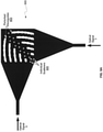
- FIG. 7B illustrates a polarization splitting grating coupler utilizing perturbed waveguides, in accordance with an exemplary embodiment of the invention.
- FIG. 7B there is shown three views of a polarization splitting grating coupler 720.
- View A shows the entire mask structure where the white region indicates areas where the mask material, which may comprise a metal such as chrome, for example, is placed to protect a silicon layer from being etched, and thus the black regions are etched away while the white areas indicate where silicon remains. This results in perpendicular light paths that direct light to a scattering pattern in the center of the polarization splitting grating coupler 720.
- View B is a close up view of the mask design for the scattering structures in the polarization splitting grating coupler 720, where perturbed waveguides 705B and 705C comprise trenches of varying width, similar to the perturbed waveguides 705A shown in FIG. 7A , but utilizing a set of waveguides for each light path in the coupler that intersect at the center line, as indicated by the dashed line.
- the perturbed waveguides 705B and 705C may be substantially perpendicular at the intersection, but the invention is not so limited, except that the angle between them may be non-zero.
- the squares at the intersection of the two sets of perturbed waveguides 705B and 705C are merely an example. Other shapes may be utilized to connect the waveguides at the center axis.
- the light in each light path, the light is scattered weakly by the perturbations when first entering the grating coupler as they are nearly parallel to the light path but then scatters more strongly when it reaches the center as it is scattered by nearly perpendicular waveguides, as in a single polarization grating coupler where propagation is approximately perpendicular to the waveguides/trenches.
- coupling to the fiber mode may be further optimized by gradually increasing the perturbation throughout the grating.
- the strong scattering near the intersections of the perturbed waveguides 705B and 705C creates a better modal overlap with the fiber mode, and thus, reduces modal loss.
- Bandwidth may also be improved as compared to conventional designs based on individual scatterers.
- perturbed waveguide designs may also improve the manufacturability of the grating couplers, by increasing the minimum feature size and by using large continuous features.
- View C shows a scanning electron microscope view (SEM) view of the structure resulting from etching the mask pattern shown in views A) and B), where the sharp corners of the mask pattern are rounded in the final structure.
- SEM scanning electron microscope view
- FIG. 7C illustrates optical measurement results for perturbed waveguide polarization splitting grating couplers, in accordance with an exemplary embodiment of the invention.
- FIG. 7C there is shown a plot of system peak loss and system 1 dB bandwidth for two designs, one being a square hole grating coupler and the other being a varying width grating coupler.
- System peak loss is defined as the lowest loss for the worst case loss curve
- FIG. 9A illustrates a polarization splitting grating coupler with perturbed waveguides as well as individual scatterers, in accordance with an exemplary embodiment of the invention.
- a polarization splitting grating coupler 900 comprising perturbed waveguides 903 and individual scatterers 905.
- the perturbed waveguide geometry can be varied with position to further optimize the modal overlap with the fiber.
- the perturbed waveguide may be incorporated with a polarization splitting grating coupler that uses individual scatterers at the intersection of the curved lines
- This embodiment comprises a combination of perturbed waveguides 903 of varying widths and individual scatters 905 at the intersection of the waveguides, which may reduce the system peak loss.
- FIG. 9B is an image of a mask design with individual scatterers at the intersection of perturbed waveguides in a polarization splitting grating coupler, in accordance with an exemplary embodiment of the invention. Referring to FIG. 9B , there is shown a close up view of the intersection of the perturbed waveguides 903 showing the individual scatterers 905.
- the shape of the individual scatterers 905 may vary along the line intersecting the perturbed waveguides 903. This may improve mode matching between grating coupler and fiber modes.
- FIG. 10A illustrates a single polarization grating coupler, in accordance with an exemplary embodiment of the invention.
- a single polarization grating coupler 1000 comprising a non-perturbed grating 1003 and perturbed waveguides 1005.
- the lithographic limit prevents arbitrarily narrow trenches from being used in grating design.
- a single polarization grating coupler comprising waveguides/trenches in one orientation, as illustrated in FIG. 4 (curvature and waveguide taper not shown)
- the first trenches typically scatter more strongly than desired, resulting is an imperfect modal overlap between the grating coupler and the fiber mode.
- Perturbed waveguides may be utilized to weakly scatter the optical signal at the beginning of the grating, allowing the grating coupler to approximate the fiber mode more closely.
- FIG. 10B illustrates a mask design for a single polarization grating coupler.
- a mask pattern comprising non-perturbed grating 1003 and perturbed waveguides.
- the perturbed waveguides 1005 provide weak scattering at the beginning of the coupler as opposed to a simple non-perturbed grating coupler, which has too strong scattering at the incident edge of the grating, causing poor optical mode mismatch.
- the scattering mode may be varied to a desired position for best match to the fiber mode.
- FIG. 11 illustrates alternative perturbation shapes in a polarization splitting grating coupler, in accordance with an exemplary embodiment of the invention.
- perturbed waveguides 1105A and 1105B there is shown perturbed waveguides 1105A and 1105B. Electromagnetic simulations were utilized to configure these perturbation shapes to reduce polarization dependence.
- a method according to claim 1 and system according to claim 2 are disclosed for grating couplers incorporating perturbed waveguides.
- the grating coupler 117A-117H, 307, 403, 703, 720, 900, 1000 may comprise a single polarization grating coupler 1000 comprising perturbed waveguides 1005 and a non-perturbed grating 1003.
- the grating coupler may comprise a polarization splitting grating coupler 720, 900, that includes two sets of perturbed waveguides 705A-705C, 903, 1005, 1105A, 1105B at a non-zero angle from each other.
- the polarization splitting grating coupler 900 may comprise individual scatterers 905 at an intersection of the sets of perturbed waveguides.
- the polarization splitting grating coupler may comprise a plurality of non-linear rows of individual scattering shapes .
- the grating couplers 117A-117H, 307, 403, 703, 720, 900, 1000 may be etched in a silicon layer on the semiconductor photonics die 130, 401 or deposited on the semiconductor photonics die.
- the grating coupler 900 may comprise individual scatterers 905 between the perturbed waveguides 903.
- x and/or y means any element of the three-element set ⁇ (x), (y), (x, y) ⁇ .
- x, y, and/or z means any element of the seven-element set ⁇ (x), (y), (z), (x, y), (x, z), (y, z), (x, y, z) ⁇ .
- exemplary means serving as a non-limiting example, instance, or illustration.
- the terms "e.g.,” and “for example” set off lists of one or more non-limiting examples, instances, or illustrations.
- a device/module/circuitry/etc. is "operable" to perform a function whenever the device/module/circuitry/etc. comprises the necessary hardware and code (if any is necessary) to perform the function, regardless of whether performance of the function is disabled, or not enabled, by some user-configurable setting.
Landscapes
- Physics & Mathematics (AREA)
- General Physics & Mathematics (AREA)
- Optics & Photonics (AREA)
- Engineering & Computer Science (AREA)
- Microelectronics & Electronic Packaging (AREA)
- Optical Integrated Circuits (AREA)
- Optical Couplings Of Light Guides (AREA)
Claims (12)
- Procédé de communication, ledit procédé comprenant :
dans une puce photonique à semi-conducteur :la communication de signaux optiques dans et/ou hors de ladite puce à semi-conducteur, en utilisant un coupleur de réseau unidimensionnel (703) sur ladite puce photonique à semi-conducteur, procédé dans lequel ledit coupleur de réseau comprend des guides d'ondes perturbés (705A), caractérisé en ce que les guides d'ondes perturbés (705A) ont une forme, une largeur ou un espacement qui varient ; etprocédé dans lequel le coupleur de réseau unidimensionnel est configuré pour diffuser une lumière incidente perpendiculairement aux guides d'ondes perturbés (705A), plus fortement qu'une lumière incidente parallèlement aux guides d'ondes perturbés (705A). - Système de communication, ledit système comprenant :
une puce photonique à semi-conducteur comprenant :un coupleur de réseau unidimensionnel sur ladite puce photonique à semi-conducteur, ledit coupleur de réseau (703) comprenant des guides d'ondes perturbés (705A) et pouvant fonctionner pour communiquer des signaux optiques dans et/ou hors de ladite puce à semi-conducteur, système dans lequel ledit coupleur de réseau comprend des guides d'ondes perturbés (705A), caractérisé en ce que les guides d'ondes perturbés (705A) ont une forme, une largeur ou un espacement qui varient ; etsystème dans lequel le coupleur de réseau unidimensionnel est configuré pour diffuser une lumière incidente perpendiculairement aux guides d'ondes perturbés (705A), plus fortement qu'une lumière incidente parallèlement aux guides d'ondes perturbés (705A). - Procédé selon la revendication 1 ou système selon la revendication 2, dans lequel lesdits guides d'ondes perturbés (705A) comprennent une largeur variable sur une longueur des guides d'ondes perturbés (705A).
- Système selon la revendication 2, dans lequel ledit coupleur de réseau (703) comprend un seul coupleur de réseau de polarisation comprenant des guides d'ondes perturbés et un réseau non perturbé.
- Procédé selon la revendication 1 ou système selon la revendication 2, dans lequel ledit coupleur de réseau (703) comprend un coupleur de réseau à séparation de polarisation.
- Procédé ou système selon la revendication 5, dans lequel ledit coupleur de réseau à séparation de polarisation comprend deux ensembles de guides d'ondes perturbés se trouvant à un angle non nul l'un par rapport à l'autre.
- Procédé ou système selon la revendication 6, dans lequel ledit coupleur de réseau à séparation de polarisation comprend des diffuseurs discrets au niveau d'une intersection desdits ensembles de guides d'ondes perturbés.
- Procédé ou système selon la revendication 5, dans lequel ledit coupleur de réseau à séparation de polarisation comprend une pluralité de rangées non linéaires de formes discrètes.
- Procédé selon la revendication 1 ou système selon la revendication 2, dans lequel lesdits coupleurs de réseau (703) sont gravés dans une couche de silicium placée sur ladite puce photonique à semi-conducteur.
- Procédé selon la revendication 1 ou système selon la revendication 2, dans lequel ledit coupleur de réseau (703) comprend des diffuseurs individuels entre lesdits guides d'ondes perturbés.
- Procédé selon la revendication 1, dans lequel lesdits coupleurs de réseau (703) sont déposés sur ladite puce photonique à semi-conducteur.
- Système selon la revendication 2, dans lequel le coupleur de réseau (703) comprend un coupleur de réseau à séparation de polarisation, et système dans lequel le coupleur de réseau comprend en outre des diffuseurs discrets.
Applications Claiming Priority (2)
| Application Number | Priority Date | Filing Date | Title |
|---|---|---|---|
| US201261690952P | 2012-07-09 | 2012-07-09 | |
| EP13175823.7A EP2685298B1 (fr) | 2012-07-09 | 2013-07-09 | Procédé et système de coupleurs à réseau incorporant des guides d'onde perturbés |
Related Parent Applications (1)
| Application Number | Title | Priority Date | Filing Date |
|---|---|---|---|
| EP13175823.7A Division EP2685298B1 (fr) | 2012-07-09 | 2013-07-09 | Procédé et système de coupleurs à réseau incorporant des guides d'onde perturbés |
Publications (2)
| Publication Number | Publication Date |
|---|---|
| EP3351983A1 EP3351983A1 (fr) | 2018-07-25 |
| EP3351983B1 true EP3351983B1 (fr) | 2022-03-23 |
Family
ID=48746398
Family Applications (2)
| Application Number | Title | Priority Date | Filing Date |
|---|---|---|---|
| EP13175823.7A Active EP2685298B1 (fr) | 2012-07-09 | 2013-07-09 | Procédé et système de coupleurs à réseau incorporant des guides d'onde perturbés |
| EP18157074.8A Active EP3351983B1 (fr) | 2012-07-09 | 2013-07-09 | Procédé et système de coupleurs à réseau incorporant des guides d'onde perturbés |
Family Applications Before (1)
| Application Number | Title | Priority Date | Filing Date |
|---|---|---|---|
| EP13175823.7A Active EP2685298B1 (fr) | 2012-07-09 | 2013-07-09 | Procédé et système de coupleurs à réseau incorporant des guides d'onde perturbés |
Country Status (2)
| Country | Link |
|---|---|
| US (7) | US9091827B2 (fr) |
| EP (2) | EP2685298B1 (fr) |
Families Citing this family (84)
| Publication number | Priority date | Publication date | Assignee | Title |
|---|---|---|---|---|
| US8625935B2 (en) * | 2010-06-15 | 2014-01-07 | Luxtera, Inc. | Method and system for integrated power combiners |
| US8942071B2 (en) * | 2011-02-04 | 2015-01-27 | Lucinda Price | Color storage and transmission systems and methods |
| US9874688B2 (en) | 2012-04-26 | 2018-01-23 | Acacia Communications, Inc. | Co-packaging photonic integrated circuits and application specific integrated circuits |
| US9091827B2 (en) | 2012-07-09 | 2015-07-28 | Luxtera, Inc. | Method and system for grating couplers incorporating perturbed waveguides |
| US9557478B2 (en) * | 2012-08-28 | 2017-01-31 | Acacia Communications, Inc. | Electronic and optical co-packaging of coherent transceiver |
| US10782479B2 (en) * | 2013-07-08 | 2020-09-22 | Luxtera Llc | Method and system for mode converters for grating couplers |
| US9549232B1 (en) * | 2013-07-11 | 2017-01-17 | Inphi Corporation | Configurable multi-rate format for communication system for silicon photonics |
| US9613886B2 (en) * | 2013-08-29 | 2017-04-04 | Industrial Technology Research Institute | Optical coupling module |
| US9577780B2 (en) | 2014-06-26 | 2017-02-21 | Luxtera, Inc. | Method and system for a polarization immune wavelength division multiplexing demultiplexer |
| JP6311558B2 (ja) * | 2014-09-29 | 2018-04-18 | 住友電気工業株式会社 | 光処理装置、光学装置 |
| WO2016068876A1 (fr) | 2014-10-28 | 2016-05-06 | Hewlett Packard Enterprise Development Lp | Interposeur photonique avec microlentilles liées sur tranche |
| WO2016069901A1 (fr) * | 2014-10-29 | 2016-05-06 | Acacia Communications, Inc. | Encapsulage de boîtier matriciel à billes optoélectroniques avec une fibre |
| US10001599B2 (en) | 2014-11-11 | 2018-06-19 | Finisar Corporation | Two-stage adiabatically coupled photonic systems |
| US9768901B2 (en) * | 2014-11-20 | 2017-09-19 | Kaiam Corp. | Planar lightwave circuit active connector |
| US9766418B2 (en) * | 2014-11-26 | 2017-09-19 | Corning Optical Communications LLC | Silicon-based optical ports, optical connector assemblies and optical connector systems |
| US10571631B2 (en) | 2015-01-05 | 2020-02-25 | The Research Foundation For The State University Of New York | Integrated photonics including waveguiding material |
| US10107962B2 (en) | 2015-02-20 | 2018-10-23 | Hewlett Packard Enterprise Development Lp | Reduction of back reflections |
| US9874693B2 (en) | 2015-06-10 | 2018-01-23 | The Research Foundation For The State University Of New York | Method and structure for integrating photonics with CMOs |
| CN107076932B (zh) * | 2015-06-11 | 2019-10-18 | 华为技术有限公司 | 一种光栅耦合器及制备方法 |
| US9910232B2 (en) * | 2015-10-21 | 2018-03-06 | Luxtera, Inc. | Method and system for a chip-on-wafer-on-substrate assembly |
| CN108474911B (zh) * | 2015-12-10 | 2020-12-11 | 博创科技英国有限公司 | 具有组合式发射器及接收器组合件的光学收发器 |
| EP3391482B1 (fr) | 2015-12-17 | 2022-11-23 | Finisar Corporation | Systèmes couplés en surface |
| US10992104B2 (en) | 2015-12-17 | 2021-04-27 | Ii-Vi Delaware, Inc. | Dual layer grating coupler |
| US9933576B2 (en) | 2015-12-29 | 2018-04-03 | Stmicroelectronics (Crolles 2) Sas | Electro-optic device with an optical grating coupler having a grating period variation and methods of formation thereof |
| US10290619B2 (en) * | 2016-01-04 | 2019-05-14 | Infinera Corporation | Photonic integrated circuit package |
| CN108885321A (zh) * | 2016-01-28 | 2018-11-23 | 申泰公司 | 光收发器 |
| WO2017151416A2 (fr) * | 2016-03-02 | 2017-09-08 | Corning Optical Communications LLC | Ensembles et agencements d'interposeur permettant de coupler au moins une fibre optique à au moins un dispositif optoélectronique |
| US9933577B2 (en) * | 2016-03-11 | 2018-04-03 | Globalfoundries Inc. | Photonics chip |
| US10749603B2 (en) * | 2016-07-14 | 2020-08-18 | Ayar Labs, Inc. | Laser module for optical data communication system within silicon interposer |
| FR3054677B1 (fr) | 2016-08-01 | 2019-05-31 | Commissariat A L'energie Atomique Et Aux Energies Alternatives | Coupleur optique multi-spectral a faibles pertes en reception |
| FR3055977B1 (fr) | 2016-09-15 | 2018-09-28 | Commissariat A L'energie Atomique Et Aux Energies Alternatives | Dispositif de couplage optique |
| EP3296783B1 (fr) * | 2016-09-15 | 2023-11-29 | IMEC vzw | Coupleur de réseau de guides d'ondes photoniques intégré |
| US10976491B2 (en) | 2016-11-23 | 2021-04-13 | The Research Foundation For The State University Of New York | Photonics interposer optoelectronics |
| EP3552281B1 (fr) * | 2016-12-06 | 2024-05-29 | Finisar Corporation | Laser à couplage de surface avec interposeur optique |
| CN117148498A (zh) * | 2017-04-19 | 2023-12-01 | 卢克斯特拉有限公司 | 用于二维模式匹配光栅耦合器的方法和系统 |
| US10698156B2 (en) | 2017-04-27 | 2020-06-30 | The Research Foundation For The State University Of New York | Wafer scale bonded active photonics interposer |
| US10394060B2 (en) * | 2017-05-17 | 2019-08-27 | Mellanox Technologies, Ltd. | Optical testing of FK modulators for silicon photonics applications |
| EP3617763B1 (fr) * | 2017-05-23 | 2024-06-19 | Huawei Technologies Co., Ltd. | Structure de module optique et procédé de fabrication associé |
| US10355805B2 (en) * | 2017-08-10 | 2019-07-16 | Luxtera, Inc. | Method and system for a free space CWDM MUX/DEMUX for integration with a grating coupler based silicon photonics platform |
| US11448823B1 (en) * | 2017-08-18 | 2022-09-20 | Acacia Communications, Inc. | Method, system, and apparatus for a LiDAR sensor with a large grating |
| TWI819834B (zh) * | 2017-11-21 | 2023-10-21 | 美商爾雅實驗室公司 | 機械傳輸套圈及使用機械傳輸套圈形成連接件的方法 |
| FR3074587B1 (fr) * | 2017-12-06 | 2020-01-03 | Commissariat A L'energie Atomique Et Aux Energies Alternatives | Puce photonique a repliement de trajet optique et structure de collimation integree |
| EP3499278A1 (fr) * | 2017-12-13 | 2019-06-19 | Thomson Licensing | Structure de réseau de diffraction comprenant plusieurs lignes de réseau |
| JP7077727B2 (ja) * | 2018-04-02 | 2022-05-31 | 株式会社豊田中央研究所 | 光偏向素子 |
| US10809456B2 (en) | 2018-04-04 | 2020-10-20 | Ii-Vi Delaware Inc. | Adiabatically coupled photonic systems with fan-out interposer |
| WO2019195441A1 (fr) | 2018-04-04 | 2019-10-10 | The Research Foundation For The State University Of New York | Structure hétérogène sur une plate-forme photonique intégrée |
| US10816724B2 (en) | 2018-04-05 | 2020-10-27 | The Research Foundation For The State University Of New York | Fabricating photonics structure light signal transmission regions |
| JP7107094B2 (ja) * | 2018-08-23 | 2022-07-27 | 富士通オプティカルコンポーネンツ株式会社 | 光デバイスおよび光送受信モジュール |
| US11435522B2 (en) | 2018-09-12 | 2022-09-06 | Ii-Vi Delaware, Inc. | Grating coupled laser for Si photonics |
| US11024617B2 (en) * | 2018-10-26 | 2021-06-01 | Micron Technology, Inc. | Semiconductor packages having photon integrated circuit (PIC) chips |
| WO2020096950A1 (fr) * | 2018-11-06 | 2020-05-14 | The Regents Of The University Of California | Nitrure d'indium et de gallium à intégration hétérogène sur des circuits intégrés photoniques au silicium |
| TWI851601B (zh) | 2018-11-21 | 2024-08-11 | 紐約州立大學研究基金會 | 光子光電系統及其製造方法 |
| US11550099B2 (en) | 2018-11-21 | 2023-01-10 | The Research Foundation For The State University Of New York | Photonics optoelectrical system |
| TWI829761B (zh) | 2018-11-21 | 2024-01-21 | 紐約州立大學研究基金會 | 具有積體雷射的光學結構 |
| US10598875B2 (en) * | 2018-12-14 | 2020-03-24 | Intel Corporation | Photonic package with a bridge between a photonic die and an optical coupling structure |
| CN109683082B (zh) * | 2018-12-26 | 2021-06-29 | 上海先方半导体有限公司 | 一种用于光学芯片的测试系统及测试方法 |
| JP7396609B2 (ja) * | 2019-02-14 | 2023-12-12 | 株式会社豊田中央研究所 | 回折格子アレイ |
| US11404850B2 (en) | 2019-04-22 | 2022-08-02 | Ii-Vi Delaware, Inc. | Dual grating-coupled lasers |
| US11493691B1 (en) * | 2019-05-15 | 2022-11-08 | Insight Lidar, Inc. | Simplified lens for photonic integrated circuits |
| FR3096791B1 (fr) * | 2019-06-03 | 2022-08-05 | St Microelectronics Sa | Dispositif optique ou optoélectronique intégré PSGC |
| GB2584681B (en) | 2019-06-11 | 2021-12-29 | Rockley Photonics Ltd | Interposer |
| CN112083526A (zh) * | 2019-06-14 | 2020-12-15 | 云晖科技有限公司 | 光学子组件结构 |
| US11428867B2 (en) * | 2019-06-14 | 2022-08-30 | Cloud Light Technology Limited | Optical subassembly structure |
| KR20220086548A (ko) | 2019-06-18 | 2022-06-23 | 더 리서치 파운데이션 포 더 스테이트 유니버시티 오브 뉴욕 | 포토닉스 구조 도전성 광 경로 제조 |
| US12092861B2 (en) * | 2019-09-27 | 2024-09-17 | Taiwan Semiconductor Manufacturing Co., Ltd. | Photonic semiconductor device and method of manufacture |
| CN112578509A (zh) | 2019-09-27 | 2021-03-30 | 台湾积体电路制造股份有限公司 | 半导体器件与系统及其制造方法 |
| US10942316B1 (en) * | 2019-10-31 | 2021-03-09 | Alliance Fiber Optic Products, Inc. | FAU connectors and assemblies employing pin-to-pin alignment |
| US11215760B2 (en) * | 2020-02-25 | 2022-01-04 | Honeywell International Inc. | Device for emission of arbitrary optical beam profiles from a chip to free space |
| US11243350B2 (en) | 2020-03-12 | 2022-02-08 | Globalfoundries U.S. Inc. | Photonic devices integrated with reflectors |
| US11347001B2 (en) * | 2020-04-01 | 2022-05-31 | Taiwan Semiconductor Manufacturing Company, Ltd. | Semiconductor structure and method of fabricating the same |
| US11567274B2 (en) * | 2020-08-17 | 2023-01-31 | Molex, Llc | Optical module |
| US11726260B2 (en) * | 2020-09-29 | 2023-08-15 | Google Llc | Substrate coupled grating couplers in photonic integrated circuits |
| US11762145B2 (en) * | 2020-10-21 | 2023-09-19 | Taiwan Semiconductor Manufacturing Company, Ltd. | Apparatus for optical coupling and system for communication |
| US11543592B2 (en) | 2020-11-13 | 2023-01-03 | Ii-Vi Delaware, Inc. | Modular assembly for opto-electronic systems |
| US11719898B2 (en) | 2021-03-03 | 2023-08-08 | Marvell Asia Pte Ltd. | Methods for co-packaging optical modules on switch package substrate |
| US11520107B2 (en) * | 2021-04-20 | 2022-12-06 | Hewlett Packard Enterprise Development Lp | Polarization diversity grating couplers with low loss and zero PDW/PDL |
| CN115407464A (zh) * | 2021-05-27 | 2022-11-29 | 华为技术有限公司 | 光引擎组件、光互连系统及网络设备 |
| CN113809499A (zh) * | 2021-08-17 | 2021-12-17 | 西安理工大学 | 一种基于tsv结构的集总参数分支线定向耦合器 |
| US12124083B2 (en) * | 2022-08-03 | 2024-10-22 | Taiwan Semiconductor Manufacturing Company Ltd. | Semiconductor structure with multi-layers film |
| US12007611B2 (en) * | 2022-08-26 | 2024-06-11 | Taiwan Semiconductor Manufacturing Company, Ltd. | Package structure having grating coupler and manufacturing method thereof |
| US12332480B2 (en) * | 2022-12-06 | 2025-06-17 | Globalfoundries U.S. Inc. | Identification system |
| US20240411086A1 (en) * | 2023-06-06 | 2024-12-12 | Taiwan Semiconductor Manufacturing Company, Ltd. | Semiconductor structure and method of fabricating the same |
| US12422623B2 (en) * | 2023-06-14 | 2025-09-23 | Taiwan Semiconductor Manufacturing Company Ltd. | Two-dimensional grating coupler and method of forming the same |
| CN117192700A (zh) * | 2023-06-29 | 2023-12-08 | 新光科技新加坡有限公司 | 一种集成光子封装结构及其形成方法 |
Family Cites Families (52)
| Publication number | Priority date | Publication date | Assignee | Title |
|---|---|---|---|---|
| US4772861A (en) | 1987-03-16 | 1988-09-20 | Harris Corporation | TE20 rectangular to crossed TE20 rectangular mode converter for TE01 circular mode launcher |
| CH679990A5 (fr) | 1989-06-08 | 1992-05-29 | Bobst Sa | |
| US5138687A (en) | 1989-09-26 | 1992-08-11 | Omron Corporation | Rib optical waveguide and method of manufacturing the same |
| US6243517B1 (en) | 1999-11-04 | 2001-06-05 | Sparkolor Corporation | Channel-switched cross-connect |
| US6293688B1 (en) | 1999-11-12 | 2001-09-25 | Sparkolor Corporation | Tapered optical waveguide coupler |
| US7773842B2 (en) * | 2001-08-27 | 2010-08-10 | Greiner Christoph M | Amplitude and phase control in distributed optical structures |
| CN1204408C (zh) | 2000-03-24 | 2005-06-01 | 汤姆森许可公司 | 采用可控制和可测试振荡器的集成电路 |
| JP3539369B2 (ja) | 2000-08-23 | 2004-07-07 | 日立電線株式会社 | アレイ導波路型光波長合分波器およびその製造方法 |
| US6697552B2 (en) | 2001-02-23 | 2004-02-24 | Lightwave Microsystems Corporation | Dendritic taper for an integrated optical wavelength router |
| US6944192B2 (en) | 2001-03-14 | 2005-09-13 | Corning Incorporated | Planar laser |
| US7212712B2 (en) | 2001-04-20 | 2007-05-01 | The Trustees Of Columbia University In The City Of New York | Coupler-multiplexer permutation switch |
| GB0220314D0 (en) | 2002-08-31 | 2002-10-09 | Univ Glasgow | Improved optical device |
| US7260289B1 (en) * | 2003-02-11 | 2007-08-21 | Luxtera, Inc. | Optical waveguide grating coupler with varying scatter cross sections |
| US7245803B2 (en) | 2003-02-11 | 2007-07-17 | Luxtera, Inc. | Optical waveguide grating coupler |
| US7006732B2 (en) * | 2003-03-21 | 2006-02-28 | Luxtera, Inc. | Polarization splitting grating couplers |
| US20040258360A1 (en) | 2003-03-25 | 2004-12-23 | Lim Desmond R. | External gain element with mode converter and high index contrast waveguide |
| US6980720B2 (en) | 2003-04-11 | 2005-12-27 | Sioptical, Inc. | Mode transformation and loss reduction in silicon waveguide structures utilizing tapered transition regions |
| US7269358B2 (en) | 2003-08-01 | 2007-09-11 | Optium Corporation | Optical transmitter for increased effective modal bandwidth transmission |
| US7136544B1 (en) | 2003-08-15 | 2006-11-14 | Luxtera, Inc. | PN diode optical modulators fabricated in strip loaded waveguides |
| KR100560387B1 (ko) | 2003-12-24 | 2006-03-13 | 한국전자통신연구원 | 단일/다중 모드 변환기, 및 이를 이용한 광 부호 분할다중 접속 시스템 |
| EP1706767B1 (fr) | 2003-12-29 | 2019-06-05 | Google LLC | Dispositif de couplage optique |
| US7397987B2 (en) * | 2004-05-06 | 2008-07-08 | California Institute Of Technology | Resonantly enhanced grating coupler |
| US7065274B2 (en) | 2004-05-27 | 2006-06-20 | Energy Conversion Devices, Inc. | Optical coupling device |
| KR100701006B1 (ko) | 2005-05-31 | 2007-03-29 | 한국전자통신연구원 | 포물선 도파로형 평행광 렌즈 및 이를 포함한 파장 가변외부 공진 레이저 다이오드 |
| EP2000836A1 (fr) * | 2007-06-07 | 2008-12-10 | Interuniversitair Microelektronica Centrum | Procédé et système pour un multiplexeur à réseau avec couplage de guides d'ondes optiques |
| US8068228B2 (en) * | 2007-08-07 | 2011-11-29 | Nanometrics Incorporated | In-plane optical metrology |
| FR2922031B1 (fr) | 2007-10-03 | 2011-07-29 | Commissariat Energie Atomique | Dispositif optique a circuits photoniques superposes, pour couplage avec un ou plusieurs guides optiques. |
| US7881575B2 (en) | 2008-01-30 | 2011-02-01 | Luxtera, Inc. | Low-loss optical interconnect |
| US20090290837A1 (en) | 2008-05-22 | 2009-11-26 | The Chinese University Of Hong Kong | Optical devices for coupling of light |
| US8168939B2 (en) | 2008-07-09 | 2012-05-01 | Luxtera, Inc. | Method and system for a light source assembly supporting direct coupling to an integrated circuit |
| EP2480917A4 (fr) * | 2009-09-23 | 2013-05-29 | Hewlett Packard Development Co | Dispositifs optiques basés sur des grilles de diffraction |
| US8781276B2 (en) * | 2010-01-29 | 2014-07-15 | Hewlett-Packard Development Company, L.P. | Grating-based optical fiber-to-waveguide interconnects |
| US8488923B2 (en) | 2010-03-29 | 2013-07-16 | Intel Corporation | Multimode optical coupler interfaces |
| WO2011137584A1 (fr) | 2010-05-05 | 2011-11-10 | 台湾超微光学股份有限公司 | Structure optique d'un micro spectromètre |
| WO2012049273A1 (fr) | 2010-10-14 | 2012-04-19 | Rwth Aachen | Coupleur entre un laser et une puce |
| US9256028B2 (en) | 2011-01-14 | 2016-02-09 | Bing Li | Dispersion-corrected arrayed waveguide grating |
| EP2694089B1 (fr) | 2011-04-05 | 2024-06-05 | Cellectis | Nouveaux échafaudages de protéine tale et leurs utilisations |
| US9885832B2 (en) | 2014-05-27 | 2018-02-06 | Skorpios Technologies, Inc. | Waveguide mode expander using amorphous silicon |
| US9746623B2 (en) | 2011-10-28 | 2017-08-29 | Seagate Technology Llc | Mode converting waveguide for heat assisted magnetic recording |
| EP2597792B1 (fr) | 2011-11-28 | 2016-04-20 | Alcatel Lucent | Traitement MIMO optique |
| US20130236193A1 (en) | 2012-03-09 | 2013-09-12 | Commscope, Inc. Of North Carolina | Optical Communications Systems that Couple Optical Signals from a Large Core Fiber to a Smaller Core Fiber and Related Methods and Apparatus |
| US8515220B1 (en) | 2012-04-12 | 2013-08-20 | Raytheon Company | Optical fiber coupler for coupling signal beams into a non-circularly shaped optical beam |
| US9091827B2 (en) | 2012-07-09 | 2015-07-28 | Luxtera, Inc. | Method and system for grating couplers incorporating perturbed waveguides |
| US9201200B2 (en) | 2012-07-26 | 2015-12-01 | Tyco Electronics Corporation | Optical assembly with diffractive optical element |
| US9122006B1 (en) | 2013-02-27 | 2015-09-01 | Aurrion, Inc. | Integrated polarization splitter and rotator |
| US8873899B2 (en) | 2013-03-14 | 2014-10-28 | Cisco Technology, Inc. | Modal rotation in optical waveguides |
| US10782479B2 (en) | 2013-07-08 | 2020-09-22 | Luxtera Llc | Method and system for mode converters for grating couplers |
| JP6548581B2 (ja) | 2014-01-24 | 2019-07-24 | 技術研究組合光電子融合基盤技術研究所 | グレーティングカプラ |
| EP2977801B1 (fr) | 2014-07-24 | 2019-11-06 | IMEC vzw | Coupleur de réseau intégré et diviseur de puissance |
| US9912408B2 (en) | 2014-10-28 | 2018-03-06 | Luxtera, Inc. | Method and system for silicon photonics wavelength division multiplexing transceivers |
| KR102364302B1 (ko) | 2015-01-27 | 2022-02-21 | 한국전자통신연구원 | 평탄한 모드 발생 장치 및 이를 구비하는 배열 도파로 격자 |
| CN117148498A (zh) | 2017-04-19 | 2023-12-01 | 卢克斯特拉有限公司 | 用于二维模式匹配光栅耦合器的方法和系统 |
-
2013
- 2013-07-08 US US13/936,408 patent/US9091827B2/en active Active
- 2013-07-09 EP EP13175823.7A patent/EP2685298B1/fr active Active
- 2013-07-09 EP EP18157074.8A patent/EP3351983B1/fr active Active
-
2015
- 2015-07-28 US US14/811,199 patent/US9417410B2/en active Active
-
2016
- 2016-08-09 US US15/232,051 patent/US9575253B2/en active Active
-
2017
- 2017-02-15 US US15/433,668 patent/US9946024B2/en active Active
-
2018
- 2018-04-11 US US15/950,897 patent/US10168481B2/en active Active
- 2018-12-20 US US16/227,890 patent/US10509170B2/en active Active
-
2019
- 2019-12-17 US US16/717,419 patent/US11137544B2/en active Active
Non-Patent Citations (1)
| Title |
|---|
| None * |
Also Published As
| Publication number | Publication date |
|---|---|
| US9575253B2 (en) | 2017-02-21 |
| US20170160469A1 (en) | 2017-06-08 |
| US20200124799A1 (en) | 2020-04-23 |
| US9417410B2 (en) | 2016-08-16 |
| US9946024B2 (en) | 2018-04-17 |
| EP2685298A1 (fr) | 2014-01-15 |
| US20150331197A1 (en) | 2015-11-19 |
| US20140010498A1 (en) | 2014-01-09 |
| US10509170B2 (en) | 2019-12-17 |
| US20180292609A1 (en) | 2018-10-11 |
| US9091827B2 (en) | 2015-07-28 |
| US11137544B2 (en) | 2021-10-05 |
| EP2685298B1 (fr) | 2018-02-21 |
| US20190121025A1 (en) | 2019-04-25 |
| US20160349449A1 (en) | 2016-12-01 |
| US10168481B2 (en) | 2019-01-01 |
| EP3351983A1 (fr) | 2018-07-25 |
Similar Documents
| Publication | Publication Date | Title |
|---|---|---|
| US11137544B2 (en) | Method and system for grating couplers incorporating perturbed waveguides | |
| EP3159721B1 (fr) | Procédé et système pour un ensemble puce-sur-tranche-sur-substrat | |
| US11143816B2 (en) | Method and system for stabilized directional couplers | |
| KR101448574B1 (ko) | 포인트 투 포인트 통신을 위한 광학 엔진 | |
| US20130209026A1 (en) | Through-substrate optical coupling to photonics chips | |
| CN102349013A (zh) | 用于点对点通信的光学引擎 | |
| US20180306986A1 (en) | Method And System For Two-Dimensional Mode-Matching Grating Couplers | |
| US11201675B2 (en) | Method and system for a bi-directional multi-wavelength receiver for standard single-mode fiber based on grating couplers | |
| US20180306977A1 (en) | Method And System For Mode Converters For Grating Couplers | |
| US10422957B2 (en) | Method and system for a low-loss optical Y-junction power splitter | |
| Li et al. | 4?×? 20 GHz silica-based AWG hybrid integrated receiver optical sub-assemblies | |
| US12529919B2 (en) | Apparatus to manipulate guided modes on a nanoscale using electro-optic effects |
Legal Events
| Date | Code | Title | Description |
|---|---|---|---|
| PUAI | Public reference made under article 153(3) epc to a published international application that has entered the european phase |
Free format text: ORIGINAL CODE: 0009012 |
|
| STAA | Information on the status of an ep patent application or granted ep patent |
Free format text: STATUS: THE APPLICATION HAS BEEN PUBLISHED |
|
| AC | Divisional application: reference to earlier application |
Ref document number: 2685298 Country of ref document: EP Kind code of ref document: P |
|
| AK | Designated contracting states |
Kind code of ref document: A1 Designated state(s): AL AT BE BG CH CY CZ DE DK EE ES FI FR GB GR HR HU IE IS IT LI LT LU LV MC MK MT NL NO PL PT RO RS SE SI SK SM TR |
|
| STAA | Information on the status of an ep patent application or granted ep patent |
Free format text: STATUS: REQUEST FOR EXAMINATION WAS MADE |
|
| 17P | Request for examination filed |
Effective date: 20190123 |
|
| RBV | Designated contracting states (corrected) |
Designated state(s): AL AT BE BG CH CY CZ DE DK EE ES FI FR GB GR HR HU IE IS IT LI LT LU LV MC MK MT NL NO PL PT RO RS SE SI SK SM TR |
|
| STAA | Information on the status of an ep patent application or granted ep patent |
Free format text: STATUS: EXAMINATION IS IN PROGRESS |
|
| 17Q | First examination report despatched |
Effective date: 20191218 |
|
| GRAP | Despatch of communication of intention to grant a patent |
Free format text: ORIGINAL CODE: EPIDOSNIGR1 |
|
| STAA | Information on the status of an ep patent application or granted ep patent |
Free format text: STATUS: GRANT OF PATENT IS INTENDED |
|
| INTG | Intention to grant announced |
Effective date: 20210518 |
|
| RIN1 | Information on inventor provided before grant (corrected) |
Inventor name: VERSLEGERS, LIEVEN Inventor name: MEKIS, ATTILA |
|
| GRAJ | Information related to disapproval of communication of intention to grant by the applicant or resumption of examination proceedings by the epo deleted |
Free format text: ORIGINAL CODE: EPIDOSDIGR1 |
|
| STAA | Information on the status of an ep patent application or granted ep patent |
Free format text: STATUS: EXAMINATION IS IN PROGRESS |
|
| GRAP | Despatch of communication of intention to grant a patent |
Free format text: ORIGINAL CODE: EPIDOSNIGR1 |
|
| STAA | Information on the status of an ep patent application or granted ep patent |
Free format text: STATUS: GRANT OF PATENT IS INTENDED |
|
| INTC | Intention to grant announced (deleted) | ||
| INTG | Intention to grant announced |
Effective date: 20211025 |
|
| GRAS | Grant fee paid |
Free format text: ORIGINAL CODE: EPIDOSNIGR3 |
|
| GRAA | (expected) grant |
Free format text: ORIGINAL CODE: 0009210 |
|
| STAA | Information on the status of an ep patent application or granted ep patent |
Free format text: STATUS: THE PATENT HAS BEEN GRANTED |
|
| AC | Divisional application: reference to earlier application |
Ref document number: 2685298 Country of ref document: EP Kind code of ref document: P |
|
| AK | Designated contracting states |
Kind code of ref document: B1 Designated state(s): AL AT BE BG CH CY CZ DE DK EE ES FI FR GB GR HR HU IE IS IT LI LT LU LV MC MK MT NL NO PL PT RO RS SE SI SK SM TR |
|
| REG | Reference to a national code |
Ref country code: GB Ref legal event code: FG4D |
|
| REG | Reference to a national code |
Ref country code: CH Ref legal event code: EP |
|
| REG | Reference to a national code |
Ref country code: DE Ref legal event code: R096 Ref document number: 602013081220 Country of ref document: DE |
|
| REG | Reference to a national code |
Ref country code: IE Ref legal event code: FG4D |
|
| REG | Reference to a national code |
Ref country code: AT Ref legal event code: REF Ref document number: 1477831 Country of ref document: AT Kind code of ref document: T Effective date: 20220415 |
|
| REG | Reference to a national code |
Ref country code: LT Ref legal event code: MG9D |
|
| REG | Reference to a national code |
Ref country code: NL Ref legal event code: MP Effective date: 20220323 |
|
| PG25 | Lapsed in a contracting state [announced via postgrant information from national office to epo] |
Ref country code: SE Free format text: LAPSE BECAUSE OF FAILURE TO SUBMIT A TRANSLATION OF THE DESCRIPTION OR TO PAY THE FEE WITHIN THE PRESCRIBED TIME-LIMIT Effective date: 20220323 Ref country code: RS Free format text: LAPSE BECAUSE OF FAILURE TO SUBMIT A TRANSLATION OF THE DESCRIPTION OR TO PAY THE FEE WITHIN THE PRESCRIBED TIME-LIMIT Effective date: 20220323 Ref country code: NO Free format text: LAPSE BECAUSE OF FAILURE TO SUBMIT A TRANSLATION OF THE DESCRIPTION OR TO PAY THE FEE WITHIN THE PRESCRIBED TIME-LIMIT Effective date: 20220623 Ref country code: LT Free format text: LAPSE BECAUSE OF FAILURE TO SUBMIT A TRANSLATION OF THE DESCRIPTION OR TO PAY THE FEE WITHIN THE PRESCRIBED TIME-LIMIT Effective date: 20220323 Ref country code: HR Free format text: LAPSE BECAUSE OF FAILURE TO SUBMIT A TRANSLATION OF THE DESCRIPTION OR TO PAY THE FEE WITHIN THE PRESCRIBED TIME-LIMIT Effective date: 20220323 Ref country code: BG Free format text: LAPSE BECAUSE OF FAILURE TO SUBMIT A TRANSLATION OF THE DESCRIPTION OR TO PAY THE FEE WITHIN THE PRESCRIBED TIME-LIMIT Effective date: 20220623 |
|
| REG | Reference to a national code |
Ref country code: AT Ref legal event code: MK05 Ref document number: 1477831 Country of ref document: AT Kind code of ref document: T Effective date: 20220323 |
|
| PG25 | Lapsed in a contracting state [announced via postgrant information from national office to epo] |
Ref country code: LV Free format text: LAPSE BECAUSE OF FAILURE TO SUBMIT A TRANSLATION OF THE DESCRIPTION OR TO PAY THE FEE WITHIN THE PRESCRIBED TIME-LIMIT Effective date: 20220323 Ref country code: GR Free format text: LAPSE BECAUSE OF FAILURE TO SUBMIT A TRANSLATION OF THE DESCRIPTION OR TO PAY THE FEE WITHIN THE PRESCRIBED TIME-LIMIT Effective date: 20220624 Ref country code: FI Free format text: LAPSE BECAUSE OF FAILURE TO SUBMIT A TRANSLATION OF THE DESCRIPTION OR TO PAY THE FEE WITHIN THE PRESCRIBED TIME-LIMIT Effective date: 20220323 |
|
| PG25 | Lapsed in a contracting state [announced via postgrant information from national office to epo] |
Ref country code: NL Free format text: LAPSE BECAUSE OF FAILURE TO SUBMIT A TRANSLATION OF THE DESCRIPTION OR TO PAY THE FEE WITHIN THE PRESCRIBED TIME-LIMIT Effective date: 20220323 |
|
| PG25 | Lapsed in a contracting state [announced via postgrant information from national office to epo] |
Ref country code: SM Free format text: LAPSE BECAUSE OF FAILURE TO SUBMIT A TRANSLATION OF THE DESCRIPTION OR TO PAY THE FEE WITHIN THE PRESCRIBED TIME-LIMIT Effective date: 20220323 Ref country code: SK Free format text: LAPSE BECAUSE OF FAILURE TO SUBMIT A TRANSLATION OF THE DESCRIPTION OR TO PAY THE FEE WITHIN THE PRESCRIBED TIME-LIMIT Effective date: 20220323 Ref country code: RO Free format text: LAPSE BECAUSE OF FAILURE TO SUBMIT A TRANSLATION OF THE DESCRIPTION OR TO PAY THE FEE WITHIN THE PRESCRIBED TIME-LIMIT Effective date: 20220323 Ref country code: PT Free format text: LAPSE BECAUSE OF FAILURE TO SUBMIT A TRANSLATION OF THE DESCRIPTION OR TO PAY THE FEE WITHIN THE PRESCRIBED TIME-LIMIT Effective date: 20220725 Ref country code: ES Free format text: LAPSE BECAUSE OF FAILURE TO SUBMIT A TRANSLATION OF THE DESCRIPTION OR TO PAY THE FEE WITHIN THE PRESCRIBED TIME-LIMIT Effective date: 20220323 Ref country code: EE Free format text: LAPSE BECAUSE OF FAILURE TO SUBMIT A TRANSLATION OF THE DESCRIPTION OR TO PAY THE FEE WITHIN THE PRESCRIBED TIME-LIMIT Effective date: 20220323 Ref country code: CZ Free format text: LAPSE BECAUSE OF FAILURE TO SUBMIT A TRANSLATION OF THE DESCRIPTION OR TO PAY THE FEE WITHIN THE PRESCRIBED TIME-LIMIT Effective date: 20220323 Ref country code: AT Free format text: LAPSE BECAUSE OF FAILURE TO SUBMIT A TRANSLATION OF THE DESCRIPTION OR TO PAY THE FEE WITHIN THE PRESCRIBED TIME-LIMIT Effective date: 20220323 |
|
| PG25 | Lapsed in a contracting state [announced via postgrant information from national office to epo] |
Ref country code: PL Free format text: LAPSE BECAUSE OF FAILURE TO SUBMIT A TRANSLATION OF THE DESCRIPTION OR TO PAY THE FEE WITHIN THE PRESCRIBED TIME-LIMIT Effective date: 20220323 Ref country code: IS Free format text: LAPSE BECAUSE OF FAILURE TO SUBMIT A TRANSLATION OF THE DESCRIPTION OR TO PAY THE FEE WITHIN THE PRESCRIBED TIME-LIMIT Effective date: 20220723 Ref country code: AL Free format text: LAPSE BECAUSE OF FAILURE TO SUBMIT A TRANSLATION OF THE DESCRIPTION OR TO PAY THE FEE WITHIN THE PRESCRIBED TIME-LIMIT Effective date: 20220323 |
|
| REG | Reference to a national code |
Ref country code: DE Ref legal event code: R097 Ref document number: 602013081220 Country of ref document: DE |
|
| PLBE | No opposition filed within time limit |
Free format text: ORIGINAL CODE: 0009261 |
|
| STAA | Information on the status of an ep patent application or granted ep patent |
Free format text: STATUS: NO OPPOSITION FILED WITHIN TIME LIMIT |
|
| PG25 | Lapsed in a contracting state [announced via postgrant information from national office to epo] |
Ref country code: DK Free format text: LAPSE BECAUSE OF FAILURE TO SUBMIT A TRANSLATION OF THE DESCRIPTION OR TO PAY THE FEE WITHIN THE PRESCRIBED TIME-LIMIT Effective date: 20220323 |
|
| PG25 | Lapsed in a contracting state [announced via postgrant information from national office to epo] |
Ref country code: MC Free format text: LAPSE BECAUSE OF FAILURE TO SUBMIT A TRANSLATION OF THE DESCRIPTION OR TO PAY THE FEE WITHIN THE PRESCRIBED TIME-LIMIT Effective date: 20220323 |
|
| REG | Reference to a national code |
Ref country code: CH Ref legal event code: PL |
|
| 26N | No opposition filed |
Effective date: 20230102 |
|
| REG | Reference to a national code |
Ref country code: BE Ref legal event code: MM Effective date: 20220731 |
|
| PG25 | Lapsed in a contracting state [announced via postgrant information from national office to epo] |
Ref country code: LU Free format text: LAPSE BECAUSE OF NON-PAYMENT OF DUE FEES Effective date: 20220709 Ref country code: LI Free format text: LAPSE BECAUSE OF NON-PAYMENT OF DUE FEES Effective date: 20220731 Ref country code: CH Free format text: LAPSE BECAUSE OF NON-PAYMENT OF DUE FEES Effective date: 20220731 |
|
| PG25 | Lapsed in a contracting state [announced via postgrant information from national office to epo] |
Ref country code: SI Free format text: LAPSE BECAUSE OF FAILURE TO SUBMIT A TRANSLATION OF THE DESCRIPTION OR TO PAY THE FEE WITHIN THE PRESCRIBED TIME-LIMIT Effective date: 20220323 Ref country code: BE Free format text: LAPSE BECAUSE OF NON-PAYMENT OF DUE FEES Effective date: 20220731 |
|
| P01 | Opt-out of the competence of the unified patent court (upc) registered |
Effective date: 20230525 |
|
| PG25 | Lapsed in a contracting state [announced via postgrant information from national office to epo] |
Ref country code: IT Free format text: LAPSE BECAUSE OF FAILURE TO SUBMIT A TRANSLATION OF THE DESCRIPTION OR TO PAY THE FEE WITHIN THE PRESCRIBED TIME-LIMIT Effective date: 20220323 Ref country code: IE Free format text: LAPSE BECAUSE OF NON-PAYMENT OF DUE FEES Effective date: 20220709 |
|
| PG25 | Lapsed in a contracting state [announced via postgrant information from national office to epo] |
Ref country code: HU Free format text: LAPSE BECAUSE OF FAILURE TO SUBMIT A TRANSLATION OF THE DESCRIPTION OR TO PAY THE FEE WITHIN THE PRESCRIBED TIME-LIMIT; INVALID AB INITIO Effective date: 20130709 |
|
| PG25 | Lapsed in a contracting state [announced via postgrant information from national office to epo] |
Ref country code: MK Free format text: LAPSE BECAUSE OF FAILURE TO SUBMIT A TRANSLATION OF THE DESCRIPTION OR TO PAY THE FEE WITHIN THE PRESCRIBED TIME-LIMIT Effective date: 20220323 Ref country code: CY Free format text: LAPSE BECAUSE OF FAILURE TO SUBMIT A TRANSLATION OF THE DESCRIPTION OR TO PAY THE FEE WITHIN THE PRESCRIBED TIME-LIMIT Effective date: 20220323 |
|
| PG25 | Lapsed in a contracting state [announced via postgrant information from national office to epo] |
Ref country code: TR Free format text: LAPSE BECAUSE OF FAILURE TO SUBMIT A TRANSLATION OF THE DESCRIPTION OR TO PAY THE FEE WITHIN THE PRESCRIBED TIME-LIMIT Effective date: 20220323 |
|
| PG25 | Lapsed in a contracting state [announced via postgrant information from national office to epo] |
Ref country code: MT Free format text: LAPSE BECAUSE OF FAILURE TO SUBMIT A TRANSLATION OF THE DESCRIPTION OR TO PAY THE FEE WITHIN THE PRESCRIBED TIME-LIMIT Effective date: 20220323 |
|
| PGFP | Annual fee paid to national office [announced via postgrant information from national office to epo] |
Ref country code: DE Payment date: 20250618 Year of fee payment: 13 |
|
| PGFP | Annual fee paid to national office [announced via postgrant information from national office to epo] |
Ref country code: GB Payment date: 20250710 Year of fee payment: 13 |
|
| PGFP | Annual fee paid to national office [announced via postgrant information from national office to epo] |
Ref country code: FR Payment date: 20250716 Year of fee payment: 13 |