EP3352206A1 - Appareil pour le traitement electrochimique de substrats semiconducteurs - Google Patents
Appareil pour le traitement electrochimique de substrats semiconducteurs Download PDFInfo
- Publication number
- EP3352206A1 EP3352206A1 EP18152649.2A EP18152649A EP3352206A1 EP 3352206 A1 EP3352206 A1 EP 3352206A1 EP 18152649 A EP18152649 A EP 18152649A EP 3352206 A1 EP3352206 A1 EP 3352206A1
- Authority
- EP
- European Patent Office
- Prior art keywords
- wafer
- processing
- processing module
- electrochemical
- transfer
- Prior art date
- Legal status (The legal status is an assumption and is not a legal conclusion. Google has not performed a legal analysis and makes no representation as to the accuracy of the status listed.)
- Granted
Links
Images

Classifications
-
- C—CHEMISTRY; METALLURGY
- C25—ELECTROLYTIC OR ELECTROPHORETIC PROCESSES; APPARATUS THEREFOR
- C25D—PROCESSES FOR THE ELECTROLYTIC OR ELECTROPHORETIC PRODUCTION OF COATINGS; ELECTROFORMING; APPARATUS THEREFOR
- C25D17/00—Constructional parts, or assemblies thereof, of cells for electrolytic coating
- C25D17/001—Apparatus specially adapted for electrolytic coating of wafers, e.g. semiconductors or solar cells
-
- H—ELECTRICITY
- H10—SEMICONDUCTOR DEVICES; ELECTRIC SOLID-STATE DEVICES NOT OTHERWISE PROVIDED FOR
- H10P—GENERIC PROCESSES OR APPARATUS FOR THE MANUFACTURE OR TREATMENT OF DEVICES COVERED BY CLASS H10
- H10P72/00—Handling or holding of wafers, substrates or devices during manufacture or treatment thereof
- H10P72/04—Apparatus for manufacture or treatment
- H10P72/0402—Apparatus for fluid treatment
-
- H—ELECTRICITY
- H10—SEMICONDUCTOR DEVICES; ELECTRIC SOLID-STATE DEVICES NOT OTHERWISE PROVIDED FOR
- H10P—GENERIC PROCESSES OR APPARATUS FOR THE MANUFACTURE OR TREATMENT OF DEVICES COVERED BY CLASS H10
- H10P72/00—Handling or holding of wafers, substrates or devices during manufacture or treatment thereof
- H10P72/04—Apparatus for manufacture or treatment
-
- C—CHEMISTRY; METALLURGY
- C25—ELECTROLYTIC OR ELECTROPHORETIC PROCESSES; APPARATUS THEREFOR
- C25D—PROCESSES FOR THE ELECTROLYTIC OR ELECTROPHORETIC PRODUCTION OF COATINGS; ELECTROFORMING; APPARATUS THEREFOR
- C25D17/00—Constructional parts, or assemblies thereof, of cells for electrolytic coating
- C25D17/004—Sealing devices
-
- C—CHEMISTRY; METALLURGY
- C25—ELECTROLYTIC OR ELECTROPHORETIC PROCESSES; APPARATUS THEREFOR
- C25D—PROCESSES FOR THE ELECTROLYTIC OR ELECTROPHORETIC PRODUCTION OF COATINGS; ELECTROFORMING; APPARATUS THEREFOR
- C25D17/00—Constructional parts, or assemblies thereof, of cells for electrolytic coating
- C25D17/06—Suspending or supporting devices for articles to be coated
-
- H—ELECTRICITY
- H10—SEMICONDUCTOR DEVICES; ELECTRIC SOLID-STATE DEVICES NOT OTHERWISE PROVIDED FOR
- H10P—GENERIC PROCESSES OR APPARATUS FOR THE MANUFACTURE OR TREATMENT OF DEVICES COVERED BY CLASS H10
- H10P72/00—Handling or holding of wafers, substrates or devices during manufacture or treatment thereof
- H10P72/04—Apparatus for manufacture or treatment
- H10P72/0441—Apparatus for sealing, encapsulating, glassing, decapsulating or the like
-
- H—ELECTRICITY
- H10—SEMICONDUCTOR DEVICES; ELECTRIC SOLID-STATE DEVICES NOT OTHERWISE PROVIDED FOR
- H10P—GENERIC PROCESSES OR APPARATUS FOR THE MANUFACTURE OR TREATMENT OF DEVICES COVERED BY CLASS H10
- H10P72/00—Handling or holding of wafers, substrates or devices during manufacture or treatment thereof
- H10P72/04—Apparatus for manufacture or treatment
- H10P72/0451—Apparatus for manufacturing or treating in a plurality of work-stations
- H10P72/0452—Apparatus for manufacturing or treating in a plurality of work-stations characterised by the layout of the process chambers
- H10P72/0458—Apparatus for manufacturing or treating in a plurality of work-stations characterised by the layout of the process chambers vertical arrangement
-
- H—ELECTRICITY
- H10—SEMICONDUCTOR DEVICES; ELECTRIC SOLID-STATE DEVICES NOT OTHERWISE PROVIDED FOR
- H10P—GENERIC PROCESSES OR APPARATUS FOR THE MANUFACTURE OR TREATMENT OF DEVICES COVERED BY CLASS H10
- H10P72/00—Handling or holding of wafers, substrates or devices during manufacture or treatment thereof
- H10P72/04—Apparatus for manufacture or treatment
- H10P72/0451—Apparatus for manufacturing or treating in a plurality of work-stations
- H10P72/0462—Apparatus for manufacturing or treating in a plurality of work-stations characterised by the construction of the processing chambers, e.g. modular processing chambers
-
- H—ELECTRICITY
- H10—SEMICONDUCTOR DEVICES; ELECTRIC SOLID-STATE DEVICES NOT OTHERWISE PROVIDED FOR
- H10P—GENERIC PROCESSES OR APPARATUS FOR THE MANUFACTURE OR TREATMENT OF DEVICES COVERED BY CLASS H10
- H10P72/00—Handling or holding of wafers, substrates or devices during manufacture or treatment thereof
- H10P72/04—Apparatus for manufacture or treatment
- H10P72/0451—Apparatus for manufacturing or treating in a plurality of work-stations
- H10P72/0464—Apparatus for manufacturing or treating in a plurality of work-stations characterised by the construction of the transfer chamber
-
- H—ELECTRICITY
- H10—SEMICONDUCTOR DEVICES; ELECTRIC SOLID-STATE DEVICES NOT OTHERWISE PROVIDED FOR
- H10P—GENERIC PROCESSES OR APPARATUS FOR THE MANUFACTURE OR TREATMENT OF DEVICES COVERED BY CLASS H10
- H10P72/00—Handling or holding of wafers, substrates or devices during manufacture or treatment thereof
- H10P72/04—Apparatus for manufacture or treatment
- H10P72/0451—Apparatus for manufacturing or treating in a plurality of work-stations
- H10P72/0468—Apparatus for manufacturing or treating in a plurality of work-stations comprising a chamber adapted to a particular process
- H10P72/0476—Apparatus for manufacturing or treating in a plurality of work-stations comprising a chamber adapted to a particular process comprising at least one plating chamber
-
- H—ELECTRICITY
- H10—SEMICONDUCTOR DEVICES; ELECTRIC SOLID-STATE DEVICES NOT OTHERWISE PROVIDED FOR
- H10P—GENERIC PROCESSES OR APPARATUS FOR THE MANUFACTURE OR TREATMENT OF DEVICES COVERED BY CLASS H10
- H10P72/00—Handling or holding of wafers, substrates or devices during manufacture or treatment thereof
- H10P72/30—Handling or holding of wafers, substrates or devices during manufacture or treatment thereof for conveying, e.g. between different workstations
- H10P72/33—Handling or holding of wafers, substrates or devices during manufacture or treatment thereof for conveying, e.g. between different workstations into and out of processing chamber
- H10P72/3302—Mechanical parts of transfer devices
-
- H—ELECTRICITY
- H10—SEMICONDUCTOR DEVICES; ELECTRIC SOLID-STATE DEVICES NOT OTHERWISE PROVIDED FOR
- H10P—GENERIC PROCESSES OR APPARATUS FOR THE MANUFACTURE OR TREATMENT OF DEVICES COVERED BY CLASS H10
- H10P72/00—Handling or holding of wafers, substrates or devices during manufacture or treatment thereof
- H10P72/30—Handling or holding of wafers, substrates or devices during manufacture or treatment thereof for conveying, e.g. between different workstations
- H10P72/34—Handling or holding of wafers, substrates or devices during manufacture or treatment thereof for conveying, e.g. between different workstations the wafers being stored in a carrier, involving loading and unloading
- H10P72/3402—Mechanical parts of transfer devices
-
- H—ELECTRICITY
- H10—SEMICONDUCTOR DEVICES; ELECTRIC SOLID-STATE DEVICES NOT OTHERWISE PROVIDED FOR
- H10P—GENERIC PROCESSES OR APPARATUS FOR THE MANUFACTURE OR TREATMENT OF DEVICES COVERED BY CLASS H10
- H10P72/00—Handling or holding of wafers, substrates or devices during manufacture or treatment thereof
- H10P72/30—Handling or holding of wafers, substrates or devices during manufacture or treatment thereof for conveying, e.g. between different workstations
- H10P72/34—Handling or holding of wafers, substrates or devices during manufacture or treatment thereof for conveying, e.g. between different workstations the wafers being stored in a carrier, involving loading and unloading
- H10P72/3404—Storage means
-
- H—ELECTRICITY
- H10—SEMICONDUCTOR DEVICES; ELECTRIC SOLID-STATE DEVICES NOT OTHERWISE PROVIDED FOR
- H10P—GENERIC PROCESSES OR APPARATUS FOR THE MANUFACTURE OR TREATMENT OF DEVICES COVERED BY CLASS H10
- H10P72/00—Handling or holding of wafers, substrates or devices during manufacture or treatment thereof
- H10P72/30—Handling or holding of wafers, substrates or devices during manufacture or treatment thereof for conveying, e.g. between different workstations
- H10P72/34—Handling or holding of wafers, substrates or devices during manufacture or treatment thereof for conveying, e.g. between different workstations the wafers being stored in a carrier, involving loading and unloading
- H10P72/3406—Handling or holding of wafers, substrates or devices during manufacture or treatment thereof for conveying, e.g. between different workstations the wafers being stored in a carrier, involving loading and unloading involving removal of lid, door or cover
-
- H—ELECTRICITY
- H10—SEMICONDUCTOR DEVICES; ELECTRIC SOLID-STATE DEVICES NOT OTHERWISE PROVIDED FOR
- H10P—GENERIC PROCESSES OR APPARATUS FOR THE MANUFACTURE OR TREATMENT OF DEVICES COVERED BY CLASS H10
- H10P72/00—Handling or holding of wafers, substrates or devices during manufacture or treatment thereof
- H10P72/30—Handling or holding of wafers, substrates or devices during manufacture or treatment thereof for conveying, e.g. between different workstations
- H10P72/34—Handling or holding of wafers, substrates or devices during manufacture or treatment thereof for conveying, e.g. between different workstations the wafers being stored in a carrier, involving loading and unloading
- H10P72/3411—Handling or holding of wafers, substrates or devices during manufacture or treatment thereof for conveying, e.g. between different workstations the wafers being stored in a carrier, involving loading and unloading involving loading and unloading of wafers
-
- H—ELECTRICITY
- H10—SEMICONDUCTOR DEVICES; ELECTRIC SOLID-STATE DEVICES NOT OTHERWISE PROVIDED FOR
- H10P—GENERIC PROCESSES OR APPARATUS FOR THE MANUFACTURE OR TREATMENT OF DEVICES COVERED BY CLASS H10
- H10P72/00—Handling or holding of wafers, substrates or devices during manufacture or treatment thereof
- H10P72/70—Handling or holding of wafers, substrates or devices during manufacture or treatment thereof for supporting or gripping
- H10P72/76—Handling or holding of wafers, substrates or devices during manufacture or treatment thereof for supporting or gripping using mechanical means, e.g. clamps or pinches
- H10P72/7602—Handling or holding of wafers, substrates or devices during manufacture or treatment thereof for supporting or gripping using mechanical means, e.g. clamps or pinches the wafers being placed on a robot blade or gripped by a gripper for conveyance
-
- H—ELECTRICITY
- H10—SEMICONDUCTOR DEVICES; ELECTRIC SOLID-STATE DEVICES NOT OTHERWISE PROVIDED FOR
- H10W—GENERIC PACKAGES, INTERCONNECTIONS, CONNECTORS OR OTHER CONSTRUCTIONAL DETAILS OF DEVICES COVERED BY CLASS H10
- H10W20/00—Interconnections in chips, wafers or substrates
- H10W20/01—Manufacture or treatment
- H10W20/031—Manufacture or treatment of conductive parts of the interconnections
- H10W20/056—Manufacture or treatment of conductive parts of the interconnections by filling conductive material into holes, grooves or trenches
- H10W20/057—Manufacture or treatment of conductive parts of the interconnections by filling conductive material into holes, grooves or trenches by selectively depositing, e.g. by using selective CVD or plating
-
- H—ELECTRICITY
- H10—SEMICONDUCTOR DEVICES; ELECTRIC SOLID-STATE DEVICES NOT OTHERWISE PROVIDED FOR
- H10P—GENERIC PROCESSES OR APPARATUS FOR THE MANUFACTURE OR TREATMENT OF DEVICES COVERED BY CLASS H10
- H10P14/00—Formation of materials, e.g. in the shape of layers or pillars
- H10P14/40—Formation of materials, e.g. in the shape of layers or pillars of conductive or resistive materials
- H10P14/46—Formation of materials, e.g. in the shape of layers or pillars of conductive or resistive materials using a liquid
- H10P14/47—Electrolytic deposition, i.e. electroplating; Electroless plating
-
- H—ELECTRICITY
- H10—SEMICONDUCTOR DEVICES; ELECTRIC SOLID-STATE DEVICES NOT OTHERWISE PROVIDED FOR
- H10W—GENERIC PACKAGES, INTERCONNECTIONS, CONNECTORS OR OTHER CONSTRUCTIONAL DETAILS OF DEVICES COVERED BY CLASS H10
- H10W20/00—Interconnections in chips, wafers or substrates
- H10W20/01—Manufacture or treatment
- H10W20/031—Manufacture or treatment of conductive parts of the interconnections
Definitions
- This invention relates to an apparatus for electrochemically processing semiconductor substrates and to associated methods of electrochemical processing.
- This invention has particular, but by no means exclusive, relevance to a plating apparatus, and to associated methods of electrochemical and electroless deposition onto semiconductor substrates.
- Electrochemical or electroless deposition processes are frequently used to form conducting layers in semiconductor device fabrication. These electroplating techniques are useful in achieving void free filling of vias, such as through silicon vias (TSVs), in particular for high aspect ratio features.
- vias such as through silicon vias (TSVs)
- TSVs through silicon vias
- copper interconnects may be formed by electrochemical deposition during damascene processing.
- Cu, Ni, SnAg and Au are known to be deposited onto silicon or compound semiconductor substrates in semiconductor packaging applications using electrochemical or electroless deposition methods.
- These plating techniques are applicable when semiconductors and components are embedded in an epoxy mould such as in Fan out Wafer level packaging (FO-WLP).
- FO-WLP Fan out Wafer level packaging
- Electrochemical deposition (ECD) processes in the semiconductor industry typically include immersing an individual semiconductor wafer into an electrolyte. A potential is applied between the wafer (acting as a cathode) and a second electrode (acting as an anode) such that species in the electrolyte are deposited on the front face of the wafer. Typically the back face of the wafer is not exposed to the electrolyte.
- the deposited layer may be removed when the wafer is acting as an anode and the second electrode acts as a cathode.
- a robot arm In automated ECD systems, a robot arm typically collects the semiconductor wafer from a loading/unloading port. This may be a cassette or front opening unified pod (FOUP).
- the robot arm moves the wafer to a wafer holding fixture which creates an electrical contact with the wafer.
- a fluid seal is formed between the wafer holding fixture and the front face of the wafer to prevent any electrolyte from contaminating the electrical contacts or the back face of the wafer.
- the wafer In "rack" systems the wafer is maintained in a substantially vertical plane and held statically in the electrolyte during processing.
- the electrolyte may be circulated within the electrolyte bath by means of a pump at relatively high flow rates, for example at 8-40 litres per minute.
- Processing steps may comprise multiple electrodeposition steps, such as deposition of a copper pillar with a Ni/SnAg cap; chemical etching steps; and numerous spin-rinse-drying (SRD), wetting and cleaning steps.
- electrodeposition steps such as deposition of a copper pillar with a Ni/SnAg cap; chemical etching steps; and numerous spin-rinse-drying (SRD), wetting and cleaning steps.
- SRD spin-rinse-drying
- each processing bath may be easily accessible by the user to permit maintenance and cleaning of the processing baths.
- Maintenance may comprise replacing the anode in an electroplating cell.
- Multiple processing baths for "fountain cell” and “rack” systems are typically arranged in one or more rows such that each processing bath can be accessed from high above by a robot arm on a linear track and by a user for maintenance.
- the wafer transport systems used in "fountain cell” and "rack” type systems may be complicated, often implementing wafer holding fixtures, an EFEM (equipment front end module) robot, and an overhead robot for transferring the wafer between processing baths and clean stations. It would be desirable for the wafer transfer between processing baths to be simplified.
- Advanced wafer processing systems often require a large number of processing baths, potentially more than 20.
- a linear arrangement of processing baths can result in the wafer processing system having a large tool footprint, potentially more than 6 m in length.
- an apparatus for processing a front face of a semiconductor wafer comprising:
- Processing may comprise chemical and/or electrochemical processing. Processing may comprise one or more of etching, electrochemical deposition, electrochemical polishing, electroless deposition, rinsing steps, cleaning steps, and drying steps.
- one of the processing modules used in the apparatus may be an etching, electrochemical deposition, electrochemical polishing, electroless deposition, rinsing, cleaning, or drying module.
- One of the processing modules used in the apparatus may be a spin rinse dry module.
- the semiconductor wafer may be a 300 mm silicon wafer, any other suitable semiconductor substrate or a rectangular panel.
- the apparatus may be suitable for processing a plurality of semiconductor wafers in parallel.
- the loading port may be a cassette or a FOUP (front opening unified pod).
- the electrochemical wafer processing module may comprise a seal which, in use, seals against a surface to define a sealed cavity in which electrochemical processing takes place.
- the seal may be an elastomeric seal.
- the seal in use, seals against a surface of the wafer to define the sealed cavity in which electrochemical processing takes place.
- the surface of the wafer that the seal seals against is an upper surface of the wafer.
- the apparatus may further comprise at least one wafer carrier arrangement onto which the wafer can be loaded.
- the wafer carrier arrangement may comprise a seal which, in use, seals against a surface of the wafer. Preferably, this seal seals against an upper surface of the wafer.
- the transfer mechanism may be configured to transfer a loaded wafer carrier arrangement between the loading port and the processing modules.
- the seal of the electrochemical wafer processing module may, in use, seal against a surface of the wafer carrier arrangement to define the sealed cavity in which electrochemical processing takes place.
- the wafer carrier arrangement also comprises an electrical contact for making an electrical contact with a loaded wafer.
- the apparatus may further comprise a wafer carrier arrangement loading station for loading the wafer onto the wafer carrier arrangement.
- the wafer carrier arrangement loading station also unloads the wafer once processing has been completed.
- the loading port may comprise the wafer carrier arrangement loading station.
- the wafer carrier arrangement loading station may be positioned between the loading port and the processing modules.
- the wafer carrier arrangement loading station may be positioned prior to the loading port so that, when the wafer is introduced to the main chamber, the wafer is loaded onto the wafer carrier arrangement before passing through the loading port.
- Adjacent processing modules in the stack preferably have a vertical separation of less than 25 cm.
- the apparatus may comprise at least one processing module that is not part of a stack.
- the transfer mechanism may comprise a transfer robot having at least one end effector for automated transfer of the wafer between the loading port and the processing modules.
- the transfer mechanism may transfer the wafer between the loading port and any of the processing modules.
- At least one of the wafer processing modules may comprise an electrochemical deposition wafer processing module.
- the front face of the wafer may comprise an electrode.
- the electrochemical processing module may further comprise a second electrode.
- An electrical bias may be applied to the wafer.
- the front face of the wafer may comprise a cathode.
- the processing modules may further comprise a tray positioned below the seal for collecting fluid.
- the processing modules may be removable from the stack.
- the processing modules may be independently removable from the stack.
- the removable nature of the processing modules may allow the processing modules to be readily accessed for the purposes of maintenance, servicing and repair work.
- the processing modules may be removable from the stack in a substantially horizontal direction.
- the processing modules may be removable from the stack by rotating, sliding or by any other suitable means.
- the apparatus may further comprise a blower for maintaining a laminar air flow in the main chamber.
- the apparatus may further comprise a wafer alignment tool.
- the apparatus may comprise at least three stacks.
- the at least three stacks may be arranged in rows or in any other suitable arrangement.
- the apparatus may be configured to process the front face of two or more semiconductor wafers in parallel.
- the method may comprise the further steps of: using the transfer mechanism to transfer the wafer from the first wafer processing module to a second wafer processing module in the stack so that the wafer is disposed substantially horizontally in the second wafer processing module; and performing a processing step on the front face of the wafer in the second wafer processing module.
- the method may comprise the further step of using the transfer mechanism to transfer the wafer from a wafer processing module to the loading port for subsequent transfer out of the apparatus.
- At least one processing step performed on the front face of the wafer may be selected from the group comprising a chemical, electrochemical, rinsing, cleaning, spinning, or drying step.
- the electrochemical processing step may comprise optionally electrochemical deposition or electrochemical etching.
- the electrochemical processing step is performed in the electrochemical wafer processing module.
- the electrochemical wafer processing module may comprise a seal which seals against a surface to define a sealed cavity in which electrochemical processing takes place.
- the seal may seal against a surface of the wafer, preferably an upper surface of the wafer, to define the sealed cavity in which electrochemical processing takes place.
- the apparatus may further comprise a wafer carrier arrangement onto which the wafer can be loaded, the wafer carrier arrangement comprising a seal which seals against a surface of the wafer, preferably an upper surface of the wafer, wherein the transfer mechanism transfers the loaded wafer carrier arrangement between the loading port and the processing modules.
- the seal of the electrochemical wafer processing module may seal against a surface of the wafer carrier arrangement to define the sealed cavity in which electrochemical processing takes place.
- the method may further comprise the step of loading the wafer onto the wafer carrier arrangement.
- the step of loading the wafer onto the wafer carrier arrangement may be performed prior to or as part of the step of using the transfer mechanism to transfer the wafer to a first wafer processing module in the stack.
- An electrical bias may be applied to the wafer during at least one processing step performed on the front face of the wafer.
- Two or more semiconductor wafers may be processed in parallel.
- a method of servicing an apparatus comprising the step of removing a wafer processing module from the stack in a substantially horizontal direction to provide access to the wafer processing module.
- Servicing may comprise performing maintenance and/or repair work on the apparatus.
- the step of removing the wafer processing module from the stack in a substantially horizontal direction may comprise rotating or sliding the processing module.
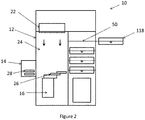
- FIG. 1 shows a wafer processing system 10 according to a first embodiment of the present invention.
- the wafer processing system 10 comprises a frame 12, a loading/unloading port 14, a robot 16 and a plurality of stacked processing modules 18a - 18d.
- Other embodiments of the present invention may incorporate fewer or more than four processing modules depending on the number of processing steps required and the vertical transfer reach of the transfer robot 16.
- the processing modules may each individually be suitable for wet chemical processing steps, such as electrochemical deposition, electrodeposition, electropolishing, chemical etching and the like; and cleaning, rinsing and drying processing steps. All positions in the stack can accommodate any module configuration and be suitable for performing any processing step.
- the hardware may be easily changed when process demands change.
- the wafer processing system 10 may also comprise local fluid supplies 20 located underneath the processing modules 18a-d.
- the local fluid supplies 20 may supply processing fluid, such as electrolyte, to each processing module 18a-d.
- Electronic control, monitoring circuitry and power supplies for the modules may be situated above the processing modules 18a-d.
- Ancillary features such as power distribution for the wafer processing system 10, bulk electrolyte storage and monitoring equipment may be situated remotely from the wafer processing system 10.
- the frame 12 encloses the components of the wafer processing system to provide a contaminant-free environment in which wafer processing can take place.
- a laminar airflow is produced by fan or blower 22 to maintain a particulate-free environment within the main chamber 24.
- the loading/unloading port 14 allows semiconductor wafers 28, such as 300 mm diameter silicon wafers, to be loaded into and unloaded from the wafer processing system 10.
- the loading/unloading port 14 may be a cassette or a FOUP (front opening unified pod).
- the port 14 may also serve as a wafer storage location in between processing steps.
- the robot 16 comprises an end effector 26 which contacts the back face of the wafer 28 (ie. the face of the wafer not subjected to processing) and transfers it to one of the processing modules 18a-d.
- the wafer 28 is handled with the front face of the wafer (ie. the face to be processed) facing upwards during all handling and processing steps.
- the use of a wafer transfer robot 16 allows automated wafer transfer between the port 14 and the processing modules 18a-d.
- the processing modules 18a-d are arranged in a vertical stack 19. Vertically stacking the processing modules 18a-d significantly reduces the tool footprint of the wafer processing system 10 compared with known systems using an equivalent number of processing modules. It is preferable to use a low profile processing module, that is, a processing module with a height of less than approximately 30 cm. More preferably a low profile module will have a height of less than 22 cm. Use of a low profile processing module enables more efficient vertical stacking.
- Known fountain cell and rack type systems require a large overhead volume in order for the substrate to enter the processing module from above. Consequently, known fountain cell and rack type systems are not well suited for efficient vertical stacking.
- Each processing module 18a-d Access may be gained to each processing module 18a-d by sliding or rotating a processing module out of the vertical stack 19 as shown in Figure 2 .
- Each processing module may be independently removable from the stack. This may be required when system intervention is required, for example, when changing an anode or to conduct a manual clean within the module.
- the isolated processing module 118 may remain connected to the wafer processing system 10 through the extendable fixture 50 to aid the replacement of the isolated processing module.
- the extendable fixture may also be attached to the frame 12. Removal of an individual processing module in this way enables complete and facile access to the isolated module.
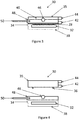
- a wet chemical processing module 30 suitable for incorporation into the wafer processing system 10 is shown in Figures 3, 4 and 5 .
- Wafer processing modules suitable for incorporation into the wafer processing system 10 are also described in EP2781630 and EP2652178 .
- the wafer is transferred from the end effector 26 of the robot arm to a movable platen assembly 32 via entry slot 34.
- the movable platen assembly 32 may be a rotatable platen assembly.
- the platen assembly 32 is raised such that the front surface of the wafer mates with the anode chamber 35.
- a fluid seal is formed between the front face of the wafer and an elastomeric seal 36.
- the elastomeric seal may be frustroconical shaped to afford a reliable fluid tight seal. Furthermore, a seal of this shape will not fall out of the chamber due to gravity or surface tension with the surface of the wetted wafer.
- the elastomeric seal may be attached to the anode chamber 35.
- a fluid tight seal is required to prevent fluid leaking from the processing module during the processing step.
- a containment tray 38 may be positioned below the platen 32 to contain any fluid leaks that may occur.
- an electrical contact to the wafer 28 may also be formed so that the wafer may serve as an electrode.
- the electrical contacts may be attached to the anode chamber 35.
- the electrical contacts may be made using titanium electrodes, Pt-coated titanium electrodes or electrodes made from any other suitable electrically conducting material.
- the electrodes may contact the wafer surface in the edge exclusion area.
- the edge exclusion area is typically ⁇ 2-3 mm from the wafer edge. The fluid tight seal prevents the electrical contacts from becoming exposed to or contaminated by the processing fluid.
- the wafer may be a cathode or an anode depending on the processing step.
- a DC bias may be applied to the wafer when acting as a cathode in an electrochemical deposition process.
- the anode in this process may be a consumable metal, such as Cu, Ni or Sn, or an inert contact, such as Pt-coated Ti or mixed metal oxide (MMO).
- the wafer 28 and the anode chamber 35 define a sealed cavity 40 in which wet chemical processing may occur.
- Wet chemical processing may comprise one or more of inter alia electrochemical or electroless deposition, electrochemical etching, and chemical etching.
- the fluid seal between the wafer 28 and the anode chamber 35 is made before any fluid enters the cavity 40. Fluid may enter and leave the cavity 40 though fluid connectors 42 and 44.
- the fluid may be an electrolyte or other suitable fluid dependent upon the processing step to be performed.
- the connector 42 is a fluid inlet whilst the connector 44 is a fluid outlet.
- the connector 42 is a fluid outlet whilst the connector 44 is a fluid inlet.
- Multiple fluid inlets help to precisely control fluid flow rate and help to ensure gas/air pockets do not form in the cavity 40, which can affect the quality of the processing step.
- an air pocket in an electrodeposition step may affect the uniformity of the resultant deposit.
- the fluid is removed from the processing module 30 after the processing step is complete and before the fluid seal between the wafer 28 and the anode chamber 35 is broken. Fluid may be removed via fluid connectors 42 and 44.
- the processing module 30 may be tilted to aid fluid removal using tilting bracket 46.
- the tilting bracket 46 is mounted on a support plate 48.
- the support plate 48 may be fixed to the anode chamber 35 via a series of retaining bolts (not shown).
- the fluid may be recycled for use in future processing steps. If required, a rinse step may be performed prior to the removal of the wafer 28 from the processing module 30.
- a processing module may be used for cleaning, rinsing, wetting or drying processes.
- the wafer 28 may be rotated by using a rotatable platen assembly.
- Cleaning fluid may be jetted towards the front face of the wafer surface for cleaning and/or wetting purposes.
- a subsequent high speed drying step may be initiated.
- the drying process may be accelerated by rotating the platen assembly, for example up to 3000 revolutions per minute (rpm).
- a spin rinse dry (SRD) module may be provided which has a rotatable platen and one or more sprays.
- the platen assembly 32 is lowered, which breaks the fluid seal.
- the end effector 26 of the robot arm may collect the wafer 28.
- the wafer 28 may be transferred to a further processing module or to the loading port 14 for temporary storage or removal from the wafer processing system 10.
- the support plate 48 may be attached to an extendable fixture 50.
- the extendable fixture 50 may remain connected to the processing module 30 when the processing module is removed from the frame 12.
- the extendable fixture may comprise a means of supplying the processing module 30 with electrical power necessary to perform electrochemical processing steps.
- the processing module 30 After the processing module 30 has been isolated from the frame 12, maintenance may be carried out on the processing module.
- the retaining bolts and fittings (not shown) may be removed to enable the anode chamber 35 to be detached from the module 30.
- the anode chamber 35 can then either be replaced by a new chamber, refurbished or replaced as appropriate.
- Access to the platen assembly 32 is provided after the anode chamber 35 has been removed. Access to the platen assembly 32 may also be achieved by removal of the containment tray 38.
- the processing modules 18a-d of the wafer processing system 10 are arranged in a vertical stack 19.
- This is not a practical arrangement for known wafer processing systems, such as "fountain cell” and "rack” type systems.
- the electrolyte bath it is necessary for the electrolyte bath to have an open top with a large depth to allow the wafer to be fully submerged.
- a vertically stacked arrangement of open topped processing baths would be vulnerable to contamination from the processing fluid in the bath above.
- a large vertical separation (or pitch) is necessary to stack such known processing baths. Without a large vertical separation, the upper baths would at least partially block the entry of the wafer into the electrolyte bath from above.
- the user's access to the processing baths for maintenance and cleaning purposes would also be at least partially restricted. Maintenance may comprise replacing the anode in an electrodeposition cell.
- the design of the processing module 30 allows processing modules to be stacked vertically in a significantly more efficient and compact arrangement without restricting the entry of the wafer into each processing module.
- Each processing module may also be readily accessed by removing the processing module from the vertical stack 19. This also allows hardware to be changed easily when process demands change.
- plastic materials such as PVC (polyvinyl chloride), HDPE (high density polyethylene), PVDF (polyvinylidene fluoride), PTFE (polytetrafluoroethylene), or PFA (perfluoroalkoxy).
- PVC polyvinyl chloride
- HDPE high density polyethylene
- PVDF polyvinylidene fluoride
- PTFE polytetrafluoroethylene
- PFA perfluoroalkoxy
- the wafer processing system 10 may be built in a cost effective fashion.
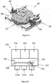
- FIG 6 shows a plan view of a second embodiment of a wafer processing system 210 in which vertical stacks 52a-c of the processing modules 18a-d may be arranged in rows.
- Processing modules 30 of the type described above in relation to Figures 3 to 5 may be suitable for use in the wafer processing system 210. Each processing module may be utilised for a different processing step as part of a larger processing procedure.
- the wafer processing system 210 may have one or more loading/unloading ports 214a-c.
- the ports 214a-c allow semiconductor wafers, such as 300 mm diameter silicon wafers, to be loaded into and unloaded from the wafer processing system.
- the loading/unloading ports 214a-c may individually be cassettes or FOUPs.
- the ports 214a-c may serve as wafer storage locations in between processing steps.
- the transport robot 216 comprises one or more end effectors 226 each of which may independently contact the back face of a wafer (ie. the face of the wafer not subjected to processing) and transfer the wafer to one of the processing modules 18a-d.
- the transport robot 216 may travel along a track 254 to enable access to each processing module 18a-d in each vertical stack 52a-c.
- the robot 216 and vertical stacks 52a-c are housed in a frame 12.
- the frame 12 provides a contaminant-free environment in which wafer processing can take place.
- a laminar airflow is produced by a fan or blower to maintain a particulate-free environment within the main chamber 224.
- a wafer alignment tool 256 may also be incorporated in the main chamber 224 to ensure correct wafer alignment during wafer transfer.
- Figure 6 shows a wafer processing system 210 incorporating three adjacent vertical stacks 52a-c, however, it would be envisaged that more or fewer vertical stacks may be used. Furthermore, other spatial arrangements, rather than a simply linear system, may be envisaged to achieve an efficient tool footprint.
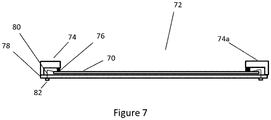
- FIG. 7 shows such an embodiment, in which a semiconductor wafer 70 is positioned on a wafer carrier fixture 72.
- the wafer carrier fixture 72 comprises a frame 74, a seal 76, and a substrate support 78 which is in communication with the frame 74.
- the frame 74 comprises an upper surface 74a and carries the seal 76.
- the wafer 70 is positioned on the substrate support 78.
- the wafer carrier fixture 72 further comprises an electrical contact 80 and a feedthrough 82 for the electrical contact 80.
- the electrical contact 80 makes electrical contact with the wafer 70 and the seal 76 seals against the wafer 70 to make a fluid tight seal.
- the components of the wafer carrier fixture 72 can be formed from any suitable materials.
- the frame 74 is typically formed from a dielectric material and the seal 76 is typically an elastomeric material such as Viton (RTM).
- a fluid seal is made between the module and the upper surface 74a of the frame 74.
- the alignment constraints for this seal are less stringent than with a fluid seal to the wafer surface.
- the skilled reader will readily appreciate that there are numerous ways of making a reliable seal to the upper surface 74a.
- the wafer carrier fixture 72/ wafer 70 assembly can be readily incorporated into the apparatus described in relation to Figures 1 to 6 without any major change in the general lay out of the system.
- the wafer 70 could be inserted into the fixture 72 after leaving the loading/unloading port 14.
- the wafer 70 would remain in the wafer carrier fixture 72 until after the final processing step is carried out.
- An additional station or other mechanism can be provided after the loading/unloading port 14 for loading and unloading the wafer onto and from the wafer carrier fixture.
- Many other arrangements for carrying the wafer and loading the wafer onto the carrier are possible. The benefit of this approach is that the seal and contacts are made only once on the wafer surface.
Landscapes
- Chemical & Material Sciences (AREA)
- Engineering & Computer Science (AREA)
- Organic Chemistry (AREA)
- Electrochemistry (AREA)
- Materials Engineering (AREA)
- Metallurgy (AREA)
- Chemical Kinetics & Catalysis (AREA)
- Life Sciences & Earth Sciences (AREA)
- Sustainable Development (AREA)
- Container, Conveyance, Adherence, Positioning, Of Wafer (AREA)
- Robotics (AREA)
- Cleaning Or Drying Semiconductors (AREA)
- Electroplating Methods And Accessories (AREA)
Applications Claiming Priority (1)
| Application Number | Priority Date | Filing Date | Title |
|---|---|---|---|
| GBGB1701166.9A GB201701166D0 (en) | 2017-01-24 | 2017-01-24 | An apparatus for electrochemically processing semiconductor substrates |
Publications (2)
| Publication Number | Publication Date |
|---|---|
| EP3352206A1 true EP3352206A1 (fr) | 2018-07-25 |
| EP3352206B1 EP3352206B1 (fr) | 2023-08-23 |
Family
ID=58463136
Family Applications (1)
| Application Number | Title | Priority Date | Filing Date |
|---|---|---|---|
| EP18152649.2A Active EP3352206B1 (fr) | 2017-01-24 | 2018-01-19 | Appareil pour le traitement electrochimique de substrats semiconducteurs |
Country Status (7)
| Country | Link |
|---|---|
| US (2) | US11066754B2 (fr) |
| EP (1) | EP3352206B1 (fr) |
| JP (1) | JP7093187B2 (fr) |
| KR (1) | KR102463961B1 (fr) |
| CN (1) | CN108346599B (fr) |
| GB (1) | GB201701166D0 (fr) |
| TW (1) | TWI739991B (fr) |
Cited By (1)
| Publication number | Priority date | Publication date | Assignee | Title |
|---|---|---|---|---|
| EP3722465A1 (fr) | 2019-04-11 | 2020-10-14 | SPTS Technologies Limited | Appareil et procédé de traitement d'un substrat |
Families Citing this family (4)
| Publication number | Priority date | Publication date | Assignee | Title |
|---|---|---|---|---|
| US12288697B2 (en) * | 2019-12-18 | 2025-04-29 | Brooks Automation (Germany), Gmbh | Core module for semiconductor production facility machinery |
| GB202018030D0 (en) | 2020-11-17 | 2020-12-30 | Spts Technologies Ltd | Spin rinse dryer with improved drying characteristics |
| KR20250075515A (ko) * | 2023-11-21 | 2025-05-28 | 엘피이 에스피에이 | 탈착식 반응 유닛이 구비된 반응기 |
| IT202300024663A1 (it) * | 2023-11-21 | 2025-05-21 | Lpe Spa | Sistema di automazione per unità di reazione removibile di un reattore epitassiale |
Citations (7)
| Publication number | Priority date | Publication date | Assignee | Title |
|---|---|---|---|---|
| WO2000040772A1 (fr) * | 1999-01-04 | 2000-07-13 | Genus, Inc. | Chambre de traitement pour procedes de depot en couches atomiques |
| US20040104120A1 (en) * | 1998-11-28 | 2004-06-03 | Hui Wang | Method and apparatus for holding and positioning semiconductor workpieces during electropolishing and/or electroplating of the workpieces |
| US6800187B1 (en) | 2001-05-31 | 2004-10-05 | Novellus Systems, Inc. | Clamshell apparatus for electrochemically treating wafers |
| US20120100709A1 (en) * | 2010-10-21 | 2012-04-26 | Yoshio Minami | Plating apparatus and plating method |
| US8500968B2 (en) | 2010-08-13 | 2013-08-06 | Applied Materials, Inc. | Deplating contacts in an electrochemical plating apparatus |
| EP2652178A2 (fr) | 2010-12-15 | 2013-10-23 | Picofluidics Limited | Appareil de dépôt électrochimique |
| EP2781630A1 (fr) | 2013-03-18 | 2014-09-24 | Picofluidics Limited | Chambre de dépôt électrochimique |
Family Cites Families (23)
| Publication number | Priority date | Publication date | Assignee | Title |
|---|---|---|---|---|
| JPH10229111A (ja) * | 1997-02-18 | 1998-08-25 | Hitachi Ltd | 半導体製造装置 |
| JP3462970B2 (ja) * | 1997-04-28 | 2003-11-05 | 三菱電機株式会社 | メッキ処理装置およびメッキ処理方法 |
| US6416647B1 (en) * | 1998-04-21 | 2002-07-09 | Applied Materials, Inc. | Electro-chemical deposition cell for face-up processing of single semiconductor substrates |
| JP2002531702A (ja) * | 1998-11-28 | 2002-09-24 | エーシーエム リサーチ,インコーポレイティド | 半導体ワークの電気めっきおよび/または電解研磨中に半導体ワークを保持して位置決めする方法および装置 |
| JP4766579B2 (ja) * | 1998-11-30 | 2011-09-07 | アプライド マテリアルズ インコーポレイテッド | 電気化学堆積装置 |
| TW527444B (en) | 1999-04-13 | 2003-04-11 | Semitool Inc | System for electrochemically processing a workpiece |
| JP4090177B2 (ja) | 2000-02-10 | 2008-05-28 | 大日本スクリーン製造株式会社 | 基板メッキ方法及びその装置 |
| US20040079633A1 (en) * | 2000-07-05 | 2004-04-29 | Applied Materials, Inc. | Apparatus for electro chemical deposition of copper metallization with the capability of in-situ thermal annealing |
| TWI222154B (en) * | 2001-02-27 | 2004-10-11 | Asm Nutool Inc | Integrated system for processing semiconductor wafers |
| TWI274393B (en) * | 2002-04-08 | 2007-02-21 | Acm Res Inc | Electropolishing and/or electroplating apparatus and methods |
| US20040262150A1 (en) * | 2002-07-18 | 2004-12-30 | Toshikazu Yajima | Plating device |
| JP2005146334A (ja) * | 2003-11-13 | 2005-06-09 | Ebara Corp | めっき方法及びめっき装置 |
| US7445697B2 (en) | 2003-10-22 | 2008-11-04 | Nexx Systems, Inc. | Method and apparatus for fluid processing a workpiece |
| US20050208774A1 (en) * | 2004-01-08 | 2005-09-22 | Akira Fukunaga | Wet processing method and processing apparatus of substrate |
| US7374391B2 (en) * | 2005-12-22 | 2008-05-20 | Applied Materials, Inc. | Substrate gripper for a substrate handling robot |
| US20110073469A1 (en) * | 2008-03-19 | 2011-03-31 | Yue Ma | Electrochemical deposition system |
| KR101051284B1 (ko) * | 2009-06-04 | 2011-07-22 | 주식회사 에스에프에이 | 박막 태양전지 제조용 화학 기상 증착 장치 |
| US20130055954A1 (en) * | 2010-05-07 | 2013-03-07 | Jeong-Ho Yoo | Integrated semiconductor-processing apparatus |
| US9017528B2 (en) | 2011-04-14 | 2015-04-28 | Tel Nexx, Inc. | Electro chemical deposition and replenishment apparatus |
| TWI719331B (zh) * | 2011-10-26 | 2021-02-21 | 美商布魯克斯自動機械公司 | 基板處理系統 |
| US9068272B2 (en) * | 2012-11-30 | 2015-06-30 | Applied Materials, Inc. | Electroplating processor with thin membrane support |
| US9818633B2 (en) * | 2014-10-17 | 2017-11-14 | Lam Research Corporation | Equipment front end module for transferring wafers and method of transferring wafers |
| DE102015109393A1 (de) * | 2015-06-12 | 2016-12-15 | Elringklinger Ag | Elektrochemische Vorrichtung und Verfahren zum Herstellen einer elektrochemischen Einheit für eine elektrochemische Vorrichtung |
-
2017
- 2017-01-24 GB GBGB1701166.9A patent/GB201701166D0/en not_active Ceased
-
2018
- 2018-01-19 EP EP18152649.2A patent/EP3352206B1/fr active Active
- 2018-01-22 US US15/876,300 patent/US11066754B2/en active Active
- 2018-01-23 TW TW107102364A patent/TWI739991B/zh active
- 2018-01-24 KR KR1020180008716A patent/KR102463961B1/ko active Active
- 2018-01-24 CN CN201810069614.3A patent/CN108346599B/zh active Active
- 2018-01-24 JP JP2018009665A patent/JP7093187B2/ja active Active
-
2021
- 2021-06-24 US US17/357,406 patent/US11643744B2/en active Active
Patent Citations (7)
| Publication number | Priority date | Publication date | Assignee | Title |
|---|---|---|---|---|
| US20040104120A1 (en) * | 1998-11-28 | 2004-06-03 | Hui Wang | Method and apparatus for holding and positioning semiconductor workpieces during electropolishing and/or electroplating of the workpieces |
| WO2000040772A1 (fr) * | 1999-01-04 | 2000-07-13 | Genus, Inc. | Chambre de traitement pour procedes de depot en couches atomiques |
| US6800187B1 (en) | 2001-05-31 | 2004-10-05 | Novellus Systems, Inc. | Clamshell apparatus for electrochemically treating wafers |
| US8500968B2 (en) | 2010-08-13 | 2013-08-06 | Applied Materials, Inc. | Deplating contacts in an electrochemical plating apparatus |
| US20120100709A1 (en) * | 2010-10-21 | 2012-04-26 | Yoshio Minami | Plating apparatus and plating method |
| EP2652178A2 (fr) | 2010-12-15 | 2013-10-23 | Picofluidics Limited | Appareil de dépôt électrochimique |
| EP2781630A1 (fr) | 2013-03-18 | 2014-09-24 | Picofluidics Limited | Chambre de dépôt électrochimique |
Cited By (2)
| Publication number | Priority date | Publication date | Assignee | Title |
|---|---|---|---|---|
| EP3722465A1 (fr) | 2019-04-11 | 2020-10-14 | SPTS Technologies Limited | Appareil et procédé de traitement d'un substrat |
| US11236433B2 (en) | 2019-04-11 | 2022-02-01 | Spts Technologies Limited | Apparatus and method for processing a substrate |
Also Published As
| Publication number | Publication date |
|---|---|
| KR20180087194A (ko) | 2018-08-01 |
| US11643744B2 (en) | 2023-05-09 |
| JP2018133560A (ja) | 2018-08-23 |
| CN108346599A (zh) | 2018-07-31 |
| US11066754B2 (en) | 2021-07-20 |
| CN108346599B (zh) | 2024-03-08 |
| EP3352206B1 (fr) | 2023-08-23 |
| US20180211856A1 (en) | 2018-07-26 |
| TW201840914A (zh) | 2018-11-16 |
| US20210317592A1 (en) | 2021-10-14 |
| KR102463961B1 (ko) | 2022-11-04 |
| JP7093187B2 (ja) | 2022-06-29 |
| GB201701166D0 (en) | 2017-03-08 |
| TWI739991B (zh) | 2021-09-21 |
Similar Documents
| Publication | Publication Date | Title |
|---|---|---|
| US11643744B2 (en) | Apparatus for electrochemically processing semiconductor substrates | |
| US7311810B2 (en) | Two position anneal chamber | |
| US7402227B2 (en) | Plating apparatus and method | |
| US6187152B1 (en) | Multiple station processing chamber and method for depositing and/or removing material on a substrate | |
| US6726823B1 (en) | Methods and apparatus for holding and positioning semiconductor workpieces during electropolishing and/or electroplating of the workpieces | |
| US6699380B1 (en) | Modular electrochemical processing system | |
| US20110073469A1 (en) | Electrochemical deposition system | |
| US10079207B2 (en) | Metallization of the wafer edge for optimized electroplating performance on resistive substrates | |
| CA2352160A1 (fr) | Procedes et appareils deupport et de positionnement de pieces a semiconducteurs lors de leur polissage electrolytique et/ou de leur placage par electrodeposition | |
| US20180223444A1 (en) | Plating apparatus and substrate holder used together with plating apparatus | |
| US9903039B2 (en) | Electrochemical deposition chamber | |
| US7967960B2 (en) | Fluid-confining apparatus | |
| US20230167571A1 (en) | Lipseal edge exclusion engineering to maintain material integrity at wafer edge | |
| US12610778B2 (en) | Wafer transfer carrier and semiconductor device manufacturing method | |
| CN101435100B (zh) | 流体区域控制装置及其操作方法 | |
| US10385471B2 (en) | Electrochemical deposition chamber | |
| JP2024053261A (ja) | 基板処理装置および基板処理方法 | |
| JP2024015542A (ja) | 基板処理装置 | |
| CN116897226A (zh) | 镀覆装置以及镀覆方法 |
Legal Events
| Date | Code | Title | Description |
|---|---|---|---|
| PUAI | Public reference made under article 153(3) epc to a published international application that has entered the european phase |
Free format text: ORIGINAL CODE: 0009012 |
|
| STAA | Information on the status of an ep patent application or granted ep patent |
Free format text: STATUS: THE APPLICATION HAS BEEN PUBLISHED |
|
| AK | Designated contracting states |
Kind code of ref document: A1 Designated state(s): AL AT BE BG CH CY CZ DE DK EE ES FI FR GB GR HR HU IE IS IT LI LT LU LV MC MK MT NL NO PL PT RO RS SE SI SK SM TR |
|
| AX | Request for extension of the european patent |
Extension state: BA ME |
|
| STAA | Information on the status of an ep patent application or granted ep patent |
Free format text: STATUS: REQUEST FOR EXAMINATION WAS MADE |
|
| 17P | Request for examination filed |
Effective date: 20190123 |
|
| RBV | Designated contracting states (corrected) |
Designated state(s): AL AT BE BG CH CY CZ DE DK EE ES FI FR GB GR HR HU IE IS IT LI LT LU LV MC MK MT NL NO PL PT RO RS SE SI SK SM TR |
|
| STAA | Information on the status of an ep patent application or granted ep patent |
Free format text: STATUS: EXAMINATION IS IN PROGRESS |
|
| 17Q | First examination report despatched |
Effective date: 20210331 |
|
| GRAP | Despatch of communication of intention to grant a patent |
Free format text: ORIGINAL CODE: EPIDOSNIGR1 |
|
| STAA | Information on the status of an ep patent application or granted ep patent |
Free format text: STATUS: GRANT OF PATENT IS INTENDED |
|
| INTG | Intention to grant announced |
Effective date: 20230315 |
|
| RIN1 | Information on inventor provided before grant (corrected) |
Inventor name: THOMAS, TREVOR Inventor name: AYRES, MARTIN Inventor name: MACNEIL, JOHN |
|
| P01 | Opt-out of the competence of the unified patent court (upc) registered |
Effective date: 20230527 |
|
| GRAS | Grant fee paid |
Free format text: ORIGINAL CODE: EPIDOSNIGR3 |
|
| GRAA | (expected) grant |
Free format text: ORIGINAL CODE: 0009210 |
|
| STAA | Information on the status of an ep patent application or granted ep patent |
Free format text: STATUS: THE PATENT HAS BEEN GRANTED |
|
| AK | Designated contracting states |
Kind code of ref document: B1 Designated state(s): AL AT BE BG CH CY CZ DE DK EE ES FI FR GB GR HR HU IE IS IT LI LT LU LV MC MK MT NL NO PL PT RO RS SE SI SK SM TR |
|
| REG | Reference to a national code |
Ref country code: GB Ref legal event code: FG4D |
|
| REG | Reference to a national code |
Ref country code: CH Ref legal event code: EP |
|
| REG | Reference to a national code |
Ref country code: DE Ref legal event code: R096 Ref document number: 602018055777 Country of ref document: DE |
|
| REG | Reference to a national code |
Ref country code: IE Ref legal event code: FG4D |
|
| REG | Reference to a national code |
Ref country code: DE Ref legal event code: R082 Ref document number: 602018055777 Country of ref document: DE Representative=s name: KANDLBINDER, MARKUS, DIPL.-PHYS., DE |
|
| REG | Reference to a national code |
Ref country code: LT Ref legal event code: MG9D |
|
| REG | Reference to a national code |
Ref country code: NL Ref legal event code: MP Effective date: 20230823 |
|
| REG | Reference to a national code |
Ref country code: AT Ref legal event code: MK05 Ref document number: 1603606 Country of ref document: AT Kind code of ref document: T Effective date: 20230823 |
|
| PG25 | Lapsed in a contracting state [announced via postgrant information from national office to epo] |
Ref country code: GR Free format text: LAPSE BECAUSE OF FAILURE TO SUBMIT A TRANSLATION OF THE DESCRIPTION OR TO PAY THE FEE WITHIN THE PRESCRIBED TIME-LIMIT Effective date: 20231124 |
|
| PG25 | Lapsed in a contracting state [announced via postgrant information from national office to epo] |
Ref country code: IS Free format text: LAPSE BECAUSE OF FAILURE TO SUBMIT A TRANSLATION OF THE DESCRIPTION OR TO PAY THE FEE WITHIN THE PRESCRIBED TIME-LIMIT Effective date: 20231223 |
|
| PG25 | Lapsed in a contracting state [announced via postgrant information from national office to epo] |
Ref country code: SE Free format text: LAPSE BECAUSE OF FAILURE TO SUBMIT A TRANSLATION OF THE DESCRIPTION OR TO PAY THE FEE WITHIN THE PRESCRIBED TIME-LIMIT Effective date: 20230823 Ref country code: RS Free format text: LAPSE BECAUSE OF FAILURE TO SUBMIT A TRANSLATION OF THE DESCRIPTION OR TO PAY THE FEE WITHIN THE PRESCRIBED TIME-LIMIT Effective date: 20230823 Ref country code: PT Free format text: LAPSE BECAUSE OF FAILURE TO SUBMIT A TRANSLATION OF THE DESCRIPTION OR TO PAY THE FEE WITHIN THE PRESCRIBED TIME-LIMIT Effective date: 20231226 Ref country code: NO Free format text: LAPSE BECAUSE OF FAILURE TO SUBMIT A TRANSLATION OF THE DESCRIPTION OR TO PAY THE FEE WITHIN THE PRESCRIBED TIME-LIMIT Effective date: 20231123 Ref country code: NL Free format text: LAPSE BECAUSE OF FAILURE TO SUBMIT A TRANSLATION OF THE DESCRIPTION OR TO PAY THE FEE WITHIN THE PRESCRIBED TIME-LIMIT Effective date: 20230823 Ref country code: LV Free format text: LAPSE BECAUSE OF FAILURE TO SUBMIT A TRANSLATION OF THE DESCRIPTION OR TO PAY THE FEE WITHIN THE PRESCRIBED TIME-LIMIT Effective date: 20230823 Ref country code: LT Free format text: LAPSE BECAUSE OF FAILURE TO SUBMIT A TRANSLATION OF THE DESCRIPTION OR TO PAY THE FEE WITHIN THE PRESCRIBED TIME-LIMIT Effective date: 20230823 Ref country code: IS Free format text: LAPSE BECAUSE OF FAILURE TO SUBMIT A TRANSLATION OF THE DESCRIPTION OR TO PAY THE FEE WITHIN THE PRESCRIBED TIME-LIMIT Effective date: 20231223 Ref country code: HR Free format text: LAPSE BECAUSE OF FAILURE TO SUBMIT A TRANSLATION OF THE DESCRIPTION OR TO PAY THE FEE WITHIN THE PRESCRIBED TIME-LIMIT Effective date: 20230823 Ref country code: GR Free format text: LAPSE BECAUSE OF FAILURE TO SUBMIT A TRANSLATION OF THE DESCRIPTION OR TO PAY THE FEE WITHIN THE PRESCRIBED TIME-LIMIT Effective date: 20231124 Ref country code: FI Free format text: LAPSE BECAUSE OF FAILURE TO SUBMIT A TRANSLATION OF THE DESCRIPTION OR TO PAY THE FEE WITHIN THE PRESCRIBED TIME-LIMIT Effective date: 20230823 Ref country code: AT Free format text: LAPSE BECAUSE OF FAILURE TO SUBMIT A TRANSLATION OF THE DESCRIPTION OR TO PAY THE FEE WITHIN THE PRESCRIBED TIME-LIMIT Effective date: 20230823 |
|
| PG25 | Lapsed in a contracting state [announced via postgrant information from national office to epo] |
Ref country code: PL Free format text: LAPSE BECAUSE OF FAILURE TO SUBMIT A TRANSLATION OF THE DESCRIPTION OR TO PAY THE FEE WITHIN THE PRESCRIBED TIME-LIMIT Effective date: 20230823 |
|
| PG25 | Lapsed in a contracting state [announced via postgrant information from national office to epo] |
Ref country code: ES Free format text: LAPSE BECAUSE OF FAILURE TO SUBMIT A TRANSLATION OF THE DESCRIPTION OR TO PAY THE FEE WITHIN THE PRESCRIBED TIME-LIMIT Effective date: 20230823 |
|
| PG25 | Lapsed in a contracting state [announced via postgrant information from national office to epo] |
Ref country code: SM Free format text: LAPSE BECAUSE OF FAILURE TO SUBMIT A TRANSLATION OF THE DESCRIPTION OR TO PAY THE FEE WITHIN THE PRESCRIBED TIME-LIMIT Effective date: 20230823 Ref country code: RO Free format text: LAPSE BECAUSE OF FAILURE TO SUBMIT A TRANSLATION OF THE DESCRIPTION OR TO PAY THE FEE WITHIN THE PRESCRIBED TIME-LIMIT Effective date: 20230823 Ref country code: ES Free format text: LAPSE BECAUSE OF FAILURE TO SUBMIT A TRANSLATION OF THE DESCRIPTION OR TO PAY THE FEE WITHIN THE PRESCRIBED TIME-LIMIT Effective date: 20230823 Ref country code: EE Free format text: LAPSE BECAUSE OF FAILURE TO SUBMIT A TRANSLATION OF THE DESCRIPTION OR TO PAY THE FEE WITHIN THE PRESCRIBED TIME-LIMIT Effective date: 20230823 Ref country code: DK Free format text: LAPSE BECAUSE OF FAILURE TO SUBMIT A TRANSLATION OF THE DESCRIPTION OR TO PAY THE FEE WITHIN THE PRESCRIBED TIME-LIMIT Effective date: 20230823 Ref country code: CZ Free format text: LAPSE BECAUSE OF FAILURE TO SUBMIT A TRANSLATION OF THE DESCRIPTION OR TO PAY THE FEE WITHIN THE PRESCRIBED TIME-LIMIT Effective date: 20230823 Ref country code: SK Free format text: LAPSE BECAUSE OF FAILURE TO SUBMIT A TRANSLATION OF THE DESCRIPTION OR TO PAY THE FEE WITHIN THE PRESCRIBED TIME-LIMIT Effective date: 20230823 |
|
| REG | Reference to a national code |
Ref country code: DE Ref legal event code: R097 Ref document number: 602018055777 Country of ref document: DE |
|
| PG25 | Lapsed in a contracting state [announced via postgrant information from national office to epo] |
Ref country code: IT Free format text: LAPSE BECAUSE OF FAILURE TO SUBMIT A TRANSLATION OF THE DESCRIPTION OR TO PAY THE FEE WITHIN THE PRESCRIBED TIME-LIMIT Effective date: 20230823 |
|
| PLBE | No opposition filed within time limit |
Free format text: ORIGINAL CODE: 0009261 |
|
| STAA | Information on the status of an ep patent application or granted ep patent |
Free format text: STATUS: NO OPPOSITION FILED WITHIN TIME LIMIT |
|
| 26N | No opposition filed |
Effective date: 20240524 |
|
| PG25 | Lapsed in a contracting state [announced via postgrant information from national office to epo] |
Ref country code: SI Free format text: LAPSE BECAUSE OF FAILURE TO SUBMIT A TRANSLATION OF THE DESCRIPTION OR TO PAY THE FEE WITHIN THE PRESCRIBED TIME-LIMIT Effective date: 20230823 |
|
| PG25 | Lapsed in a contracting state [announced via postgrant information from national office to epo] |
Ref country code: MC Free format text: LAPSE BECAUSE OF FAILURE TO SUBMIT A TRANSLATION OF THE DESCRIPTION OR TO PAY THE FEE WITHIN THE PRESCRIBED TIME-LIMIT Effective date: 20230823 |
|
| PG25 | Lapsed in a contracting state [announced via postgrant information from national office to epo] |
Ref country code: MC Free format text: LAPSE BECAUSE OF FAILURE TO SUBMIT A TRANSLATION OF THE DESCRIPTION OR TO PAY THE FEE WITHIN THE PRESCRIBED TIME-LIMIT Effective date: 20230823 |
|
| REG | Reference to a national code |
Ref country code: CH Ref legal event code: PL |
|
| PG25 | Lapsed in a contracting state [announced via postgrant information from national office to epo] |
Ref country code: LU Free format text: LAPSE BECAUSE OF NON-PAYMENT OF DUE FEES Effective date: 20240119 |
|
| GBPC | Gb: european patent ceased through non-payment of renewal fee |
Effective date: 20240119 |
|
| PG25 | Lapsed in a contracting state [announced via postgrant information from national office to epo] |
Ref country code: LU Free format text: LAPSE BECAUSE OF NON-PAYMENT OF DUE FEES Effective date: 20240119 |
|
| PG25 | Lapsed in a contracting state [announced via postgrant information from national office to epo] |
Ref country code: GB Free format text: LAPSE BECAUSE OF NON-PAYMENT OF DUE FEES Effective date: 20240119 |
|
| PG25 | Lapsed in a contracting state [announced via postgrant information from national office to epo] |
Ref country code: BE Free format text: LAPSE BECAUSE OF NON-PAYMENT OF DUE FEES Effective date: 20240131 |
|
| PG25 | Lapsed in a contracting state [announced via postgrant information from national office to epo] |
Ref country code: CH Free format text: LAPSE BECAUSE OF NON-PAYMENT OF DUE FEES Effective date: 20240131 |
|
| PG25 | Lapsed in a contracting state [announced via postgrant information from national office to epo] |
Ref country code: GB Free format text: LAPSE BECAUSE OF NON-PAYMENT OF DUE FEES Effective date: 20240119 Ref country code: CH Free format text: LAPSE BECAUSE OF NON-PAYMENT OF DUE FEES Effective date: 20240131 Ref country code: BE Free format text: LAPSE BECAUSE OF NON-PAYMENT OF DUE FEES Effective date: 20240131 |
|
| REG | Reference to a national code |
Ref country code: BE Ref legal event code: MM Effective date: 20240131 |
|
| PG25 | Lapsed in a contracting state [announced via postgrant information from national office to epo] |
Ref country code: BG Free format text: LAPSE BECAUSE OF FAILURE TO SUBMIT A TRANSLATION OF THE DESCRIPTION OR TO PAY THE FEE WITHIN THE PRESCRIBED TIME-LIMIT Effective date: 20230823 |
|
| PG25 | Lapsed in a contracting state [announced via postgrant information from national office to epo] |
Ref country code: BG Free format text: LAPSE BECAUSE OF FAILURE TO SUBMIT A TRANSLATION OF THE DESCRIPTION OR TO PAY THE FEE WITHIN THE PRESCRIBED TIME-LIMIT Effective date: 20230823 |
|
| PG25 | Lapsed in a contracting state [announced via postgrant information from national office to epo] |
Ref country code: IE Free format text: LAPSE BECAUSE OF NON-PAYMENT OF DUE FEES Effective date: 20240119 |
|
| PG25 | Lapsed in a contracting state [announced via postgrant information from national office to epo] |
Ref country code: IE Free format text: LAPSE BECAUSE OF NON-PAYMENT OF DUE FEES Effective date: 20240119 |
|
| PG25 | Lapsed in a contracting state [announced via postgrant information from national office to epo] |
Ref country code: CY Free format text: LAPSE BECAUSE OF FAILURE TO SUBMIT A TRANSLATION OF THE DESCRIPTION OR TO PAY THE FEE WITHIN THE PRESCRIBED TIME-LIMIT; INVALID AB INITIO Effective date: 20180119 |
|
| PG25 | Lapsed in a contracting state [announced via postgrant information from national office to epo] |
Ref country code: HU Free format text: LAPSE BECAUSE OF FAILURE TO SUBMIT A TRANSLATION OF THE DESCRIPTION OR TO PAY THE FEE WITHIN THE PRESCRIBED TIME-LIMIT; INVALID AB INITIO Effective date: 20180119 |
|
| REG | Reference to a national code |
Ref country code: DE Ref legal event code: R079 Ref document number: 602018055777 Country of ref document: DE Free format text: PREVIOUS MAIN CLASS: H01L0021670000 Ipc: H10P0072000000 |
|
| PG25 | Lapsed in a contracting state [announced via postgrant information from national office to epo] |
Ref country code: TR Free format text: LAPSE BECAUSE OF FAILURE TO SUBMIT A TRANSLATION OF THE DESCRIPTION OR TO PAY THE FEE WITHIN THE PRESCRIBED TIME-LIMIT Effective date: 20230823 |
|
| PGFP | Annual fee paid to national office [announced via postgrant information from national office to epo] |
Ref country code: DE Payment date: 20260128 Year of fee payment: 9 |
|
| PGFP | Annual fee paid to national office [announced via postgrant information from national office to epo] |
Ref country code: FR Payment date: 20260126 Year of fee payment: 9 |