EP3352307A1 - Dispositif et procédé de fabrication d'un tel dispositif destinés à la transmission d'un signal électrique et/ou d'un signal de données dans un véhicule - Google Patents
Dispositif et procédé de fabrication d'un tel dispositif destinés à la transmission d'un signal électrique et/ou d'un signal de données dans un véhicule Download PDFInfo
- Publication number
- EP3352307A1 EP3352307A1 EP18152535.3A EP18152535A EP3352307A1 EP 3352307 A1 EP3352307 A1 EP 3352307A1 EP 18152535 A EP18152535 A EP 18152535A EP 3352307 A1 EP3352307 A1 EP 3352307A1
- Authority
- EP
- European Patent Office
- Prior art keywords
- electrical conductor
- shield
- contact element
- arrangement
- contact
- Prior art date
- Legal status (The legal status is an assumption and is not a legal conclusion. Google has not performed a legal analysis and makes no representation as to the accuracy of the status listed.)
- Withdrawn
Links
- 238000004519 manufacturing process Methods 0.000 title claims abstract description 17
- 239000004020 conductor Substances 0.000 claims abstract description 180
- 239000011159 matrix material Substances 0.000 claims abstract description 33
- 229920000642 polymer Polymers 0.000 claims abstract description 31
- 239000000463 material Substances 0.000 claims description 26
- 230000002093 peripheral effect Effects 0.000 claims description 16
- 238000007789 sealing Methods 0.000 claims description 15
- 239000002245 particle Substances 0.000 claims description 8
- OKTJSMMVPCPJKN-UHFFFAOYSA-N Carbon Chemical compound [C] OKTJSMMVPCPJKN-UHFFFAOYSA-N 0.000 claims description 6
- 229910021393 carbon nanotube Inorganic materials 0.000 claims description 6
- 239000002041 carbon nanotube Substances 0.000 claims description 6
- RYGMFSIKBFXOCR-UHFFFAOYSA-N Copper Chemical compound [Cu] RYGMFSIKBFXOCR-UHFFFAOYSA-N 0.000 claims description 5
- 229910052802 copper Inorganic materials 0.000 claims description 5
- 239000010949 copper Substances 0.000 claims description 5
- 229910052782 aluminium Inorganic materials 0.000 claims description 4
- XAGFODPZIPBFFR-UHFFFAOYSA-N aluminium Chemical compound [Al] XAGFODPZIPBFFR-UHFFFAOYSA-N 0.000 claims description 4
- 239000004760 aramid Substances 0.000 claims description 4
- 229920003235 aromatic polyamide Polymers 0.000 claims description 4
- 229920001940 conductive polymer Polymers 0.000 claims description 4
- 239000011236 particulate material Substances 0.000 claims description 3
- 229920000767 polyaniline Polymers 0.000 claims description 3
- 229920000128 polypyrrole Polymers 0.000 claims description 3
- 229920000123 polythiophene Polymers 0.000 claims description 3
- 239000006229 carbon black Substances 0.000 claims description 2
- 238000000034 method Methods 0.000 description 19
- 238000011161 development Methods 0.000 description 13
- 230000018109 developmental process Effects 0.000 description 13
- 230000005670 electromagnetic radiation Effects 0.000 description 6
- 230000005540 biological transmission Effects 0.000 description 3
- 230000008054 signal transmission Effects 0.000 description 3
- 238000005452 bending Methods 0.000 description 2
- 239000003989 dielectric material Substances 0.000 description 2
- 238000005253 cladding Methods 0.000 description 1
- 238000010276 construction Methods 0.000 description 1
- 230000001419 dependent effect Effects 0.000 description 1
- 229910003460 diamond Inorganic materials 0.000 description 1
- 239000010432 diamond Substances 0.000 description 1
- 230000000694 effects Effects 0.000 description 1
- 238000010292 electrical insulation Methods 0.000 description 1
- 238000001746 injection moulding Methods 0.000 description 1
- 238000003780 insertion Methods 0.000 description 1
- 230000037431 insertion Effects 0.000 description 1
- 239000011810 insulating material Substances 0.000 description 1
- 239000007788 liquid Substances 0.000 description 1
- 239000002923 metal particle Substances 0.000 description 1
- 239000004033 plastic Substances 0.000 description 1
- 230000008719 thickening Effects 0.000 description 1
Images



Classifications
-
- H—ELECTRICITY
- H01—ELECTRIC ELEMENTS
- H01R—ELECTRICALLY-CONDUCTIVE CONNECTIONS; STRUCTURAL ASSOCIATIONS OF A PLURALITY OF MUTUALLY-INSULATED ELECTRICAL CONNECTING ELEMENTS; COUPLING DEVICES; CURRENT COLLECTORS
- H01R13/00—Details of coupling devices of the kinds covered by groups H01R12/70 or H01R24/00 - H01R33/00
- H01R13/02—Contact members
- H01R13/03—Contact members characterised by the material, e.g. plating, or coating materials
-
- H—ELECTRICITY
- H01—ELECTRIC ELEMENTS
- H01B—CABLES; CONDUCTORS; INSULATORS; SELECTION OF MATERIALS FOR THEIR CONDUCTIVE, INSULATING OR DIELECTRIC PROPERTIES
- H01B1/00—Conductors or conductive bodies characterised by the conductive materials; Selection of materials as conductors
- H01B1/20—Conductive material dispersed in non-conductive organic material
-
- H—ELECTRICITY
- H01—ELECTRIC ELEMENTS
- H01R—ELECTRICALLY-CONDUCTIVE CONNECTIONS; STRUCTURAL ASSOCIATIONS OF A PLURALITY OF MUTUALLY-INSULATED ELECTRICAL CONNECTING ELEMENTS; COUPLING DEVICES; CURRENT COLLECTORS
- H01R2201/00—Connectors or connections adapted for particular applications
- H01R2201/26—Connectors or connections adapted for particular applications for vehicles
Definitions
- the invention relates to an arrangement according to claim 1 and a method for producing such an arrangement according to claim 15.
- an improved arrangement for transmitting a current signal and / or a data signal in a vehicle comprising an electrical lead and a contactor connected to the electrical lead, wherein the electrical line comprises at least one electrical conductor and an electrical conductor covering and electrically insulating insulating layer, wherein the contact device comprises at least one contact element, wherein the contact element is connected to one end of the electrical conductor, wherein the contact element and the electrical conductor are electrically conductive wherein the contact element and the electrical conductor have at least one polymer matrix.
- This embodiment has the advantage that the contact element and the electrical conductor can be manufactured in a particularly simple and cost-effective manner, preferably in a common production method.
- the polymer matrix is formed in one piece and of the same material in the contact element and the electrical conductor, wherein preferably the polymer matrix comprises at least one of the following materials: aramid, intrinsically conductive polymer, polypyrrole, polythiophene, polyaniline.
- the electrical conductor and the contact element have an electrically conductive material arranged in the polymer matrix, wherein preferably the electrically conductive material comprises carbon nanotubes and / or particulate material, preferably copper particles and / or aluminum particles and / or carbon black.
- the electrical line comprises an electrically conductive shield, the insulating layer encasing the electrical conductor and the shield encasing the insulating layer, the insulating layer electrically insulating the shield from the electrical conductor, the shield and the further contact element being electrically conductive are and the further contact element is connected to one end of the shield, wherein the contact device has a further contact element, wherein the further contact element and the shield have a further polymer matrix.
- the further contact element and the shield preferably have an electrically conductive further material arranged in the further polymer matrix.
- the further electrically conductive material has at least one of the following materials: carbon nanotubes, metal particles, in particular copper particles, aluminum particles.
- the electrical conductor and / or the shield have an at least partially star-shaped and / or circular and / or polygonal and / or elliptical cross section. Additionally or alternatively, the shield is arranged coaxially with the electrical conductor.
- the electrical conductor has a first portion and a second portion, wherein the second portion is disposed inclined to the first portion and connected to the first portion, wherein the first portion and the second portion define a gap, wherein the Shielding is at least partially arranged in the intermediate space. In this way, an electrical capacitance between the electrical conductor and the shield can be selectively set.
- the electrical line has a further electrical conductor, a further insulating layer and a further shield, the further electrical conductor being arranged parallel to the electrical conductor in the longitudinal direction, the further insulating layer encasing the further electrical conductor, wherein the further shield encases the further insulating layer.
- the electrical conductor and the further electrical conductor preferably have the same electrically conductive material, wherein the shield and the further shield preferably have the same electrically conductive further material, wherein the shield and the further shield are electrically connected to each other or between the shield and the additional shielding an additional insulating layer is arranged.
- the electrical line to a soul, wherein the electrical conductor surrounds the soul circumferentially.
- the electrical line can transmit particularly high tensile forces.
- the contact element is arranged adjacent to a free end of the electrical conductor, wherein the contact element circumferentially surrounds the electrical conductor in sections, wherein the contact element has a contact surface for electrical contacting.
- the contact device has a carrier, wherein the contact element is arranged on the carrier, wherein the carrier has a carrier surface, wherein preferably the contact surface and the carrier surface are arranged in a common plane, or wherein the contact surface is curved and over the carrier surface protrudes.
- the carrier is arranged in the longitudinal direction of the electrical line extending or transverse to the longitudinal direction to the electrical line.
- the contact element and the further contact element are arranged on opposite sides of the carrier.
- the insulating layer comprises a first insulating section and a second insulating section.
- the first insulating portion and the second insulating portion are disposed adjacent to each other in the longitudinal direction of the electric wire.
- the second insulating portion is disposed between the shield and the electrical conductor.
- In the longitudinal direction between one end of the shield and the contact element of the first insulating portion is arranged.
- the contact element overlapping, preferably arranged completely overlapping the second insulating portion. In this way, a particularly compact contact device can be provided.
- the contact device comprises a sealing element arranged on an outer peripheral surface of the second insulating section.
- the second insulating section has a predefined electrical resistance as a function of a resistance of the contact element, wherein the predefined resistance of the insulating section is selected such that the contact device has a predefined terminating resistor.
- the electrical conduit comprises a sheath, the sheath encasing the shield, the sheath electrically isolating the shield from an environment.
- the sheath is connected to a housing of the contact device, wherein the sheath and the housing are integrally formed and of uniform material.
- the housing on a side facing away from the electrical conductor end a latching element, wherein the latching element is formed in a locking receptacle a further insertable into the housing contact element of another arrangement to intervene.
- a support element and / or a sealing element is arranged on the circumference of the casing.
- an improved arrangement as described above can be made by forming, in particular extruding and / or spun, the electrical conductor from the polymer matrix, with the electrical conductor being covered with the insulating layer, the shielding around the insulating layer is formed, in particular extruded and / or spun, wherein the contact element is formed on the electrical conductor, and / or wherein the electrical conductor, and / or wherein the insulating layer is extruded.
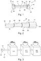
- FIG. 1 shows a schematic representation of an arrangement 10.
- the arrangement 10 is designed as a line arrangement, in particular as a connection cable, in particular signal transmission cable, in particular as a data cable, for signal transmission and / or data transmission in a motor vehicle.
- the arrangement 10 can also be designed for Hochstromübertagung example, in the motor vehicle.
- the arrangement 10 comprises a first contact device 15, preferably a second contact device 20 and an electrical line 25.
- the first contact device 15 has a first housing 30, a first contact element 35 and preferably a second contact element 40. In the first housing 30, the first contact element 35 and the second contact element 40 are arranged.
- the second contact device 20 has a second housing 45, a third contact element 50 preferably and a fourth contact element 55.
- the third and fourth contact members 50, 55 are disposed in the second housing 45.
- the electrical line 25 is exemplified as a coaxial cable. Other embodiments of the electrical line 25 are also conceivable.
- the electrical line 25 comprises at least one electrical conductor 60 and an insulating layer 65 sheathing the electrical conductor 60, a shield 70 sheathing the insulating layer 65, and a sheath 75 sheathing the shield 70 Shielding 70 and the sheath 75, a further electrical conductor 70 and / or instead of the sheath 75, a further insulating layer 75 may be provided.
- the electrical conductor 60 is electrically connected at its first end to the first contact element 35. At its second end, the electrical conductor 60 is connected to the third contact element 50.
- the electrical conductor 60 and the contact elements 35, 50 are designed to be electrically conductive in order to transmit a current and / or a current signal and / or a data signal between the first contact element 35 and the third contact element 50.
- the power transmission can be used to transmit a supply energy. Also, a data signal may be modulated onto the transmitted stream.
- the shield 70 is electrically connected at its first end to the second contact element 40 and at its second end to the fourth contact element 55.
- the shield 70, the second contact element 40 and the fourth contact element 55 are formed electrically conductive.
- the shield 70 connects electrically the second contact element 40 with the fourth contact element 55.
- the shield 70 shields the electrical conductor 25, for example, from electrical and / or magnetic fields, for example, from an environment.
- the insulating layer 65 preferably comprises a dielectric material and electrically insulates the electrical conductor 60 from the shield 70.
- the sheath 75 electrically insulates the shield 70 from an environment 80.
- the sheath 75 may also include a dielectric material for this purpose.
- the first contact device 15 is exemplified in the embodiment as a plug contact.
- the second contact device 20 as Socket contact trained.
- other embodiments of the first contact device 15 and / or the second contact device 20 are conceivable.
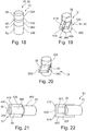
- FIG. 2 shows a schematic representation of the in FIG. 1 shown arrangement 10 with the electrical line 25 according to a first embodiment.
- the first contact element 35 and the electrical conductor 60 are integrally formed of the same material and have a first polymer matrix 85.
- the first contact element 35 and the electrical conductor 60 may optionally have an electrically conductive material 90 arranged in the first polymer matrix 85.
- the insulating layer 65 electrically insulates the electrical conductor 60 from the shield 70.
- the shield 70 is exemplified by a hollow cylinder, while the electrical conductor 60 is a circular one Cross section has.
- the electrical conductor 60 and the shield 70 are arranged coaxially with each other.
- the shield 70 and the second contact element 40 as well as preferably the fourth contact element 55 are integrally formed of the same material and preferably have a second polymer matrix 95.
- the shielding 70 and the second contact element 40 and preferably the fourth contact element 55 have a further electrically conductive material 100, wherein in the second polymer matrix 95 of the further electrically conductive material 100 is arranged.
- the further electrically conductive material 100 may be identical to the electrically conductive material 90.
- first polymer matrix 85 and / or the second polymer matrix 85 95 on at least one of the following materials: aramid, intrinsically conductive polymer, polypyrrole, polythiophene, polyaniline.
- Another advantage is, in particular when using only a non-electrically conductive polymer, for example aramid, as material for the polymer matrix 85, 95, when the electrically conductive material 90 and / or the further electrically conductive material 100 is provided and preferably carbon nanotubes and / or particulate material, preferably copper particles and / or aluminum particles.
- a non-electrically conductive polymer for example aramid
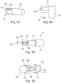
- FIG. 3 shows a schematic representation of a manufacturing process in the Figures 1 and 2 described arrangement 10th
- a first method step 200 the first contact element 35, the electrical conductor 60 and the third contact element 50 are produced by introducing the electrically conductive material 90 with the first polymer matrix 85 into a mold.
- the first polymer matrix 85 and / or the electrically conductive material 90 may be extruded or spun together or sequentially.
- the electrically conductive material 90 has carbon nanotubes, these are produced in the first method step 200 according to one of the known production methods, for example grown.
- the first contact element 35, the electrical conductor 60 and the third contact element 50 are integrally formed of the same material.
- the common production in the common first method step 200 has the advantage that an electrical resistance is avoided by avoiding contact resistances between the first contact element 35 and the electrical conductor 60 and between the third contact element 50 and the electrical conductor 60.
- the insulating layer 65 is applied to the electrical conductor 60, preferably extruded.
- the second contact element 40, the shield 70 and the fourth contact element 55 are produced by introducing the further electrically conductive material 100 with the second polymer matrix 95 into a further mold.
- the second polymer matrix 95 and / or the further electrically conductive material 100 may be extruded or spun together or sequentially.
- the further electrically conductive material 100 has carbon nanotubes, these are produced in the third method step 210 according to one of the known production methods, for example grown, sprayed or spun.
- the second contact element 40, the shield 70 and the fourth contact element 55 are integrally formed and of uniform material.
- the joint production in the third method step 210 has the advantage that an electrical resistance is avoided by avoiding contact resistances between the second contact element 40 and the shield 70 and between the fourth contact element 55 and the shield 70.
- a fourth method step 215 the sheath 75 is applied to the shield 70, preferably extruded.
- the housing 30, 45 is preferably injection-molded onto the contact elements 35, 40, 50, 55 and is preferably connected to the jacket 75.
- This embodiment has the advantage that in a production line, the arrangement 10 can be produced particularly quickly and inexpensively.
- FIG. 4 shows a sectional view through the electrical line 25.
- the electrical line 25 has opposite to in FIG. 2 shown electrical line 25 in addition to a soul 105, which is encompassed by the electrical conductor 60 circumferentially.
- the core 105 may comprise a particularly high tensile strength material, with preferably the tensile strength of the material of the core 105 being greater than the tensile strength of the materials of the electrical conductor 60 and / or the insulating layer 65 and / or the shield 70 and / or the cladding 75.
- the core 105 serves to transmit a mechanical tensile load within the electrical line 25 between the first contact device 15 and the second contact device 20 and to avoid mechanical overloading of the electrical conductor 60 and / or the shield 70.
- the electrical conductor 60 and the shield 70 are arranged concentrically with each other.
- the electrical conductor 60 and the shield 70 have a star-shaped configuration.
- the sheath 75 has a circular outer peripheral surface 110. Due to the star-shaped configuration of the electrical conductor 60 and the shield 70, the electrical conductor 60 and the shield 70 can be selectively adjusted to one another in such a way that, at a predefined frequency, the electrical conductor 60 and the shield 70 have a predefined electrical capacitance to each other.
- FIG. 5 shows a sectional view through an electrical line 25 according to a third embodiment.
- the electric wire 25 is similar to that in FIG. 4 formed electrical line 25 is formed.
- the outer peripheral surface 110 of the casing 75 is formed corresponding to the star-shaped configuration of the electrical conductor 60 and the shield 70. As a result, a space requirement of the electrical line 25 can be reduced.
- the electric wire 25 is similar to those in the FIGS. 1, 2 . 4 and 5 formed embodiments shown.
- FIG. 6 shows a sectional view through an electrical line 25 according to a fourth embodiment.
- the electrical conductor 60 is formed with a circular cross section.
- the electrical conductor 60 is arranged centrally. Concentric with the electrical conductor 60 between the shield 70 and the electrical conductor 60 alternately further electrical conductors 115 and further insulating layers 120 are arranged.
- the further insulating layer 120 arranged adjacent to two electrical conductors 60, 115 in each case electrically isolates the electrical conductors 60, 115 adjoining the further insulating layer 120 from one another.
- the further electrical conductor 115 and the shield 70 are formed by way of example ring and surround each of the radially inner side disposed insulating layer 65, 120th
- FIG. 7 shows a sectional view through an electrical line 25 according to a fifth embodiment.
- the electric wire 25 is similar to those in the FIGS. 1, 2 and 4 to 6 formed embodiments shown.
- the electrical conductor 60 has a plurality of parallel offset transversely in the first portions 125 which are electrically connected to each other via a perpendicular to the first portion 125 arranged second portion 130 of the electrical conductor 60.
- the first and second sections 125, 130 define a gap 135.
- the shield 70 has, for example, a third section 140, a fourth section 145 and a fifth section 150.
- the third portion 140 is formed as a secant to the fifth portion 150 and electrically connected at its respective ends to the fifth portion 150.
- the third section 140 is arranged parallel to the first section 125 in a parallel manner.
- the fifth section 150 is annular and extends radially outward to the third and fourth sections 140, 145.
- the fourth section 145 is radially outwardly connected to the fifth section 150 and extends parallel to the first section 125 on a side facing away from the third section 140 side.
- the fourth section 145 engages in the intermediate space 135.
- the gap 135 is filled with the insulating layer 65 between the fourth portion 145 and the first and second portions 125, 130.
- the embodiment shown has the advantage that a particularly high electrical capacitance in the electrical line 25 between the shield 70 and the electrical conductor 60 can be provided.
- FIGS. 1, 2 . 4 to 7 shown geometric configurations of the electrical conductor 60 and the shield 70 may alternatively be formed differently and in their geometric configuration to such effect adapted specifically that an outer Circumference surface of the electrical conductor 60 and / or the shield 70 is selectively increased in order to produce a particularly large conductive surface or turn off unwanted frequencies or to increase an electrical capacitance between the electrical conductor 60 and the shield 70 targeted to disturbances within the electrical line 25 targeted to minimize.
- FIG. 8 shows a sectional view through an electrical line 25 according to a sixth embodiment.
- the electrical line 25 has the electrical conductor 60 and at least one further electrical conductor 160.
- the further electrical conductor 160 is arranged transversely spaced from the electrical conductor 60.
- the further electrical conductor 160 and the electrical conductor 60 are parallel to each other.
- the electrical conductor 60 and the further electrical conductor 160 preferably have the same material.
- the further electrical conductor 160 also has the first polymer matrix 85 and the electrically conductive material 90.
- the electrical conductor 60 and the further electrical conductor 160 are arranged in the common plane.
- a further shield 165 is provided for each additional electrical conductor 160.
- the further shielding 165 like the shielding 70, is configured in the form of an annular ring, for example, and is guided around the further electrical conductor 160 at a distance.
- a further insulating layer 170 is provided in each case.
- the further insulating layer 170 preferably has the same material as the insulating layer 65.
- the further insulating layer 170 electrically insulates the further shield 165 from the further electrical conductor 160.
- the further shield 165 has a contact contact 175 with the shield 70.
- Shield 165 and the shield 70 into each other.
- the further shield 165 is configured identically to the shield 70. Also, other embodiments are conceivable.
- the further shield 165 and the shield 70 have the same further electrically conductive material 100 and the second polymer matrix 95.
- an additional insulating layer may also be provided between the shield 70 and the further shield 165.
- the further shield 165 and the shield 70 are surrounded on the outside by the casing 75.
- the further shield 165 and the shield 70 may be embedded in the casing 75.
- This embodiment has the advantage that the shield 70 and the further shield 165 can be connected to a common electrical potential.
- FIG. 9 shows a sectional view through an electrical line 25 according to a seventh embodiment.
- the electric wire 25 is similar to that in FIG FIG. 8 formed electrical line 25 is formed.
- the electrical conductor 60 and the other electrical conductors 160 are arranged in a diamond shape.
- the touch contact 175 is arranged in the transverse direction of the electrical line 25 between the further electrical conductor 160 and the electrical conductor 60.
- FIG. 10 shows a sectional view through an electrical line 25 according to an eighth embodiment.
- the electric wire 25 is similar to that in FIG Figures 2 and 4 formed electrical line 25 is formed. Deviating from this, the electrical conductor 60 is annular. The electrical conductor 60 surrounds the soul 105. Furthermore, a cost of materials for the electrical conductor 60 is reduced. This embodiment is especially at Transmission of high-frequency signals via the electrical conductor 60 is advantageous since the signal transmission takes place essentially via an edge layer of the electrical conductor 60.
- FIG. 11 shows a perspective view of a cable 185.
- the cable 185 has a plurality of electrical lines 25, which are arranged side by side. In this case, each electrical line 25 is laterally connected to at least one of the next electrical lines 25 via the respective associated sheath 75.
- the electrical line 25 may, as in the FIGS. 1 to 10 be described described.
- FIG. 3 The above in FIG. 3
- the method described can be used to produce the in FIG. 11 shown cable 185 are adapted in that the juxtaposed electrical lines 25 are produced together in the manufacturing method described above. As a result, a particularly inexpensive ribbon cable can be produced.
- FIG. 12 shows a schematic representation of a system 300.
- the system 300 includes an assembly 10 and another assembly 305.
- the further arrangement 305 may be identical to the arrangement 10.
- the arrangement 10 and the further arrangement 305 can, for example, as in the FIGS. 1 to 11 be explained explained.
- the first contact device 15 of the arrangement 10 is designed as a socket contact
- the second contact device 20 of the further arrangement 305 is designed as a plug contact.
- the housing 30, 45 is continuous for electromagnetic radiation 315, preferably for light, in particular for light having at least one wavelength in the infrared range.
- a device 310 emitting the electromagnetic radiation 315 which is preferably designed as a laser, switchably provides the electromagnetic radiation 315.
- the electromagnetic radiation 315 penetrates the housing 30, 45 and connects the first contact element 35 to the third contact element 50 in a material-locking manner, preferably by means of a welded connection.
- the device 310 can also connect the first polymer matrix 85 and the electrically conductive material 90 in the first contact element 35 to the second polymer matrix 95 and the further electrically conductive material 100 by means of the electromagnetic radiation 315.
- a particularly stable electrical connection between the arrangement 10 and the further arrangement 305 can be provided.
- a permanent contact between the arrangement 10 and the further arrangement 305 is ensured.
- FIG. 13 shows a longitudinal section through an assembly 10 in another embodiment.
- the arrangement 10 is similar to that in FIG FIG. 2 shown embodiment of the arrangement 10 is formed. Deviating from this, the first contact element 35 in the transverse direction of the electrical line 25 is formed wider than in FIG. 2 , The first contact element 35 is arranged adjacent to a free end 320 of the electrical conductor 60.
- the first contact element 35 is integrally formed and the same material with the electrical conductor 60, wherein symbolically by dashed line of the electrical conductor 60 in FIG. 13 is shown.
- the first contact element 35 surrounds the electrical conductor 60 on the circumference and has a first contact surface 325 on an outer peripheral surface.
- the first contact surface 325 serves for electrical contacting of the first contact element 35.
- the first contact element 35 is arranged in the longitudinal direction adjacent to the insulating layer 65.
- an overlap in the longitudinal direction means that when two components, for example the first contact element 35 and the insulating layer 65 are projected into a projection plane that is oriented perpendicular to the longitudinal direction that at least partially cover components (for example, the insulating layer 65 and the first contact element 35) in the projection plane.
- the insulating layer 65 has an outer circumferential surface 330 which is formed identically to the first contact surface 325. It is particularly advantageous if the first contact element 35 and the insulating layer 65 completely overlap in the longitudinal direction.
- the first contact element 35 and the electrical conductor 60 may together in the first method step 200, as in FIG FIG. 3 explained. Also, the first contact element 35 can be subsequently attached in a further additional process step to the electrical conductor 60, in particular molded or welded, be.
- the insulating layer 65 has a first insulating portion 335 and a second insulating portion 340.
- the second insulating section 340 is peripherally encompassed by the shield 70 and ends at the first contact element 35 facing the end 345 of the shield 70.
- the first insulating portion 335 is circumferentially free and is not encompassed by the shield 70 on the circumference.
- the first insulating portion 335 is disposed between the end 345 of the shield 70 and the first contact element 35. Due to the longitudinally adjacent arrangement of the first insulating section 335 and the second insulating section 340, a creeping distance between the first contact element 35 and the end 345 of the shield 70 are made particularly long.
- a creepage distance is understood to be the shortest distance along a surface of an insulating material, in the embodiment of the insulating layer 65.
- the second contact element 40 is arranged in the longitudinal direction between one end 355 of the casing 75 on a side of the casing 75 facing the first contact element 35 and the insulating layer 65.
- the second contact element 40 is itself formed by the shield 70 in the embodiment.
- the second contact element 40 similar to the first contact element 35 on the electrical conductor 60, be formed as a thickening on the shield 70 and engage around the shield 70 on the outside.
- the second contact element 40 has a second contact surface 360. It is particularly advantageous if the second contact surface 360 and the first contact surface 325 in the transverse direction, preferably also the outer peripheral surface 330 of the insulating layer 65, are identical and overlap in the longitudinal direction.
- FIG. 14 shows a perspective view of another embodiment of the arrangement 10th
- the arrangement 10 is similar to that in FIG FIG. 13 formed arrangement 10 is formed. Deviating from this, the electrical line 25 is formed as a single line, so that in the in the FIGS. 1 to 13 shown shield 70 and the Sheath 75 is dispensed with. Further, opposite FIG. 13 also dispensed with the second contact element 40.
- the arrangement 10 On the outer circumferential surface 330 of the insulating layer 65, preferably adjacent to the first contact element 35, the arrangement 10 has a sealing element 365.
- the sealing element 365 is designed to be wider in the transverse direction of the arrangement 10 than the first contact surface 325.
- the sealing element 365 engages around the outer peripheral surface 330 of the insulating layer 65.
- a support member 370 is arranged instead of the sealing element 365.
- the support element 370 may, for example, a particularly pressure-resistant material, in particular a plastic and / or the material of the insulating layer 65, have.
- the support member 370 has on the circumference a support surface 375, which is formed by way of example cylindrical. The support element 370 derives a transverse force F Q via the support surface 375 substantially without deformation of the support element 370 from the arrangement 10.
- FIG. 15 shows a perspective view of an arrangement 10 in a development.
- the assembly 10 is substantially identical to that in FIG. 14 formed arrangement 10 is formed. Notwithstanding, the arrangement 10 has both the sealing element 365 and the supporting element 375.
- the support member 375 is disposed radially outward on the outer peripheral surface 330 of the insulating layer 65. Further, the support member 375 is spaced longitudinally from the seal member 365.
- the support member 370 surrounds the insulating layer 65 circumferentially. In this case, the support element 370 extends in the longitudinal direction in a direction away from the first contact element 35 direction.
- the first contact device 15 is inserted in a receptacle 380, for example the second contact device 20 of the further arrangement 305.
- the receptacle 380 has an inner receiving surface 385, which may be cylindrical, for example.
- the arrangement 10 is inserted so far into the receptacle 380, so that both the sealing element 365 and the support element 370 bear peripherally on the receiving surface 385. Further, the outer peripheral surface 330 of the insulating layer 65 is spaced from the receiving surface 385. Is in the assembly 10, for example, introduced via the electric line 25, the transverse force F Q, the transverse force F Q can be particularly well drained into the receptacle 380, and so deformation of the sealing element 365 can be avoided on the support 370th As a result, an introduction of liquids toward the first contact element 35 can be avoided.
- FIG. 16 shows a perspective view of an arrangement 10 in a further development.
- the assembly 10 is substantially identical to that in FIG. 15 shown embodiment of the arrangement 10 is formed.
- a kink protection 390 is additionally provided, which is arranged adjacent to the support element 370 on a side facing away from the first contact element 35 side.
- the anti-buckling 390 may be designed to taper away from the support element 370 in the longitudinal direction.
- the anti-kink 390 prevents a too small radius for the electrical line 25 and thus kinking of the electrical conductor 60, so that the electrical line 25 is not mechanically damaged.
- FIG. 17 shows a perspective view of an arrangement 10 in a further development.
- FIG. 17 shown arrangement 10 is essentially a combination of the in the FIGS. 13 to 16 shown developments of the arrangements 10th
- the support member 370 is disposed between the first contact member 35 and the second contact member 40 in the longitudinal direction. In a longitudinal direction facing away from the first contact element 35, the sealing element 365 is arranged adjacent to the second contact element 40.
- the support element 370 also serves for electrical insulation of the first contact element 35 to the second contact element 40.
- the creepage distance between the first contact element 35 and the second contact element 40 is kept particularly large by the radially wide configuration of the support element 370.
- the arrangement 10 has an additional additional support element 391.
- the further support element 391 is arranged in the longitudinal direction on a side facing away from the second contact element 40 side of the sealing element 365 spaced from the sealing element 365.
- the further support element 391 surrounds the casing 75.
- the further support element 391 is of annular design and has on its circumference a further support surface 395, which has the same configuration as the support surface 375 of the support element 370.
- the further support element 391 is also arranged in the receptacle 380.
- This refinement has the advantage that particularly high transverse forces F Q from the electric line 25 can be supported on the receptacle 380 via the supporting element 370 and the further supporting element 391.
- FIG. 18 shows a perspective view of an arrangement 10 in a further development.
- the arrangement 10 may be similar to that in FIG. 2 and 13 be formed embodiment shown.
- the first contact surface 325, the outer peripheral surface 330 of the insulating layer 65, the second contact surface 360 of the second contact element 40 and an outer peripheral surface 400 of the sheath 75 are formed in the transverse direction identical to each other.
- a cylindrical shape of the assembly 10 can be provided at the end of the assembly 10 with a uniform outer contour.
- FIG. 19 shows a perspective view of an arrangement 10 in a further development.
- the arrangement 10 is similar to that in FIG FIG. 18 formed arrangement 10 is formed.
- the contact device 15, 20 has a carrier 405.
- the carrier 405 has a plate-like design and extends transversely to the longitudinal direction of the arrangement 10.
- the first contact element 35 is arranged on a first carrier surface 410 of the carrier 405.
- the second support surface 415 is disposed opposite to the first support surface 410, in the embodiment opposite in the longitudinal direction.
- the first contact surface 325 and the first support surface 410 are arranged in a common plane.
- the second contact surface 360 and the second support surface 415 are arranged in a further common plane.
- the further plane and the plane are arranged parallel to one another.
- the contact element 35, 40 arranged on the carrier 405.
- an offset arrangement of the contact elements 35, 40 on the carrier 405 is conceivable.
- FIG. 20 shows a perspective view of an arrangement 10 in a further development.
- the arrangement 10 is similar to that in FIG FIG. 19 shown embodiment of the arrangement 10 is formed. Deviating from this, the contact elements 35, 40 are arranged laterally offset from one another on the carrier 405. In this case, the contact elements 35, 40 are each arranged opposite each other in the longitudinal direction at the same height.
- the contact elements 35, 40 extend over the entire longitudinal extent of the carrier 405 and cover each of the side surfaces of the carrier 405th
- FIG. 21 shows a perspective view of an arrangement 10 in a further development.
- the arrangement 10 is similar to that in FIGS FIGS. 19 and 20 formed arrangement 10 is formed. Notwithstanding this, the carrier 405 extends in the longitudinal direction and preferably projects beyond the outer peripheral surface 400 of the casing 75.
- the carrier 405 and the contact elements 35, 40 have the same width in the longitudinal direction.
- the contact surface 325, 360 formed by way of example bale-shaped.
- the first contact surface 325 projects beyond the first carrier surface 410 and the second contact surface 360 via the second carrier surface 415 of the carrier 405.
- FIG. 22 shows a perspective view of an arrangement 10 in a further development.
- the arrangement 10 and is essentially a combination of the in FIG. 19 and FIG. 21 features shown.
- the contact element 35, 40 is shorter in the longitudinal direction than the carrier 405, so that at a free end 420 of the carrier 405 on a side facing away from the electrical line 25 an end face 425 spaced from the contact element 35, 40 is.
- the contact element 35, 40 is planar, wherein the first contact surface 325 is arranged in a common plane with the first carrier surface 410.
- FIG. 23 shows an arrangement 10 in a further development.
- the arrangement 10 essentially corresponds to that in FIG. 22 Deviating from this, the carrier 405 is arranged transversely to the longitudinal direction of the electrical line 25.
- FIG. 24 shows a perspective view of an arrangement 10 in a further development.
- the arrangement 10 is similar to that in FIG. 23 formed arrangement 10 is formed. Deviating from this, the first carrier surface 410 and the second carrier surface 415 are aligned parallel to the longitudinal direction of the electrical line 25. The carrier 405 is also aligned transversely to the longitudinal direction of the electrical lead 25.
- FIG. 25 shows a perspective view of an arrangement 10 in a further development.
- the arrangement 10 is similar to that in FIGS Figures 2 . 13 and 18 formed arrangement 10 is formed. Deviating from this, the first contact element 35 is arranged in the insulating layer 65 offset from the free end 320 of the electrical conductor 60. The first contact surface 325 and the outer Peripheral surface 330 of the insulating layer 65 extend on a common plane. In this case, the first contact element 35 is arranged in the longitudinal direction between the electrical conductor 60 and the shield 70, wherein the first contact element 35 is connected to the electrical conductor 60 inside and is electrically insulated from the shield 70.
- FIG. 26 shows a perspective view of a sectional view through a system 300 in another embodiment.
- the system 300 exemplifies the in FIG. 24 shown arrangement 10.
- the system 300 may be one of the FIGS. 1 . 23 or 25 have explained arrangement 10.
- the system 300 further includes another assembly 305.
- the further arrangement 305 has the second contact device 20.
- the second contact device 20 is designed as a socket contact and comprises a socket 430 with a first socket surface 435 and a second socket surface 440.
- the first socket surface 435 is arranged parallel to the second socket surface 440.
- the first socket surface 435 and the second socket surface 440 extend parallel to the longitudinal direction in two transversely offset differently arranged planes.
- the third contact element 50 is arranged on the first socket surface 445 and the fourth contact element 55 is arranged on the second socket surface 440. In the inserted state, the first contact element 35 contacts the third contact element 50 and the second contact element 40 electrically contacts the fourth contact element 55.
- FIG. 27 shows a sectional view through a system 300 in another embodiment.
- the system 300 is similar to that in FIG. 26 shown system 300 formed. Deviating from this, the carrier 405 is dispensed with.
- the first contact device 15 is exemplary as in FIG. 2 explained educated.
- the second Contact device 20 of the further arrangement 305 is designed as a socket contact.
- the third contact element 50 of the further arrangement 305 has a first receptacle 500 and the fourth contact element 55 has a second receptacle 505.
- the second receptacle 505 has a greater transverse extent than the first receptacle 500.
- the first receptacle 500 is in this case corresponding to the first contact element 35 and the second receptacle 505 is formed corresponding to the second contact element 40.
- This embodiment has the advantage that the third contact element 50 can be formed integrally with the electrical conductor 60 of the further arrangement 305, so that the third contact element 50, the first polymer matrix 85 of the electrical conductor 60 and the electrically conductive material 90 of the electrical conductor 60 has.
- the insulating layer 65 projects frontally beyond the first receptacle 500 on a side facing away from the electrical conductor 60 side.
- the second receptacle 505 protrudes frontally beyond an end 510 of the insulating layer 65.
- the casing 75 projects beyond the second receptacle 505 on the front side.
- the second contact device 20 is configured stepwise from outside to inside in the longitudinal direction.
- This embodiment has the advantage that an unwanted contacting of the second receptacle 505 by the first contact element 35 upon insertion of the first contact device 15 into the second contact device 20 of the further arrangement 305 is reliably avoided.
- FIG. 28 shows a sectional view through a variant of in FIG. 27 shown arrangement 10th
- the first contact device 15 is substantially identical to the one in FIG. 27 formed first contact means 15 is formed. Deviating from this is instead of in FIG. 27 shown arrangement 10 of the first contact device 15 to the electrical line 25 in the longitudinal direction in FIG. 28 the first contact device 15 is arranged transversely to the longitudinal direction of the electrical line 25.
- FIG. 29 shows a sectional view through a system 300 according to another embodiment.
- the system 300 is similar to that in FIG. 27 described system 300 is formed. Deviating from this, the system 300 has a first latching device 600 and a second latching device 605. Of course, one of the two locking devices 600, 605 can also be dispensed with.
- the first latching device 600 has a first latching element 610 and a first latching receptacle 615.
- the first latching element 610 is arranged on the inside on the second receptacle 505.
- the first latching element 610 extends inwards.
- the first latching receptacle 615 is provided in the second contact element 40 of the arrangement 10.
- the first latching receptacle 615 is formed corresponding to the first latching element 610.
- the first latching element 610 engages in the first latching receptacle 615 and secures the arrangement 10 to the further arrangement 305, so that unintentional release of the arrangement 10 from the further arrangement 305 is avoided.
- the second latching device 605 has a second latching element 620 on the inside of the casing 75 of the further arrangement 305, and a second latching receptacle 625 in the casing 75 of the arrangement 10.
- the second latching receptacle 625 is arranged, for example, circumferentially in the casing 75. In the assembled state, the second latching element 620 engages in the second latching receptacle 625.
- FIG. 30 shows a perspective view of the arrangement 10.
- the assembly 10 substantially corresponds to the in FIG. 29
- the first latching receptacle 615 is shorter in the longitudinal direction than the first contact element 35.
- the arrangement of the first latching receptacle 615 in the second contact element 40 can further provide an additional secure electrical connection between the second latching element 610 Contact element 40 and the fourth contact element 55 are ensured.
- FIGS. 1 to 30 shown embodiment of the arrangement 10, 305 and the corresponding system 300 has the advantage that a particularly simple and inexpensive designed arrangement 10, 305 can be provided.
- a construction volume of the arrangement 10, 305, in particular of the contact device 15, 20, can be kept particularly low. Furthermore, can be dispensed with metallic contact elements. Likewise, the contact device 15, 20 can be produced together in the production of the electrical line 25 in a common manufacturing process, so that the assembly 10, 305 is particularly cost-effective. Furthermore, the contact element 35, 40, 50, 55 can be injected into a housing 30, 45. This is of particular advantage in particular by means of a multi-component injection molding method, since different zones with different properties can thereby be created.
- a cross section of the electrical conductor 60 and the shield 70 can be kept particularly low. As a result, particularly tight bending radii are possible. Also, a smaller cross section of the electrical conductor 60 and the shield 70 is less sensitive to mechanical alternating bending loads.
Landscapes
- Physics & Mathematics (AREA)
- Chemical & Material Sciences (AREA)
- Dispersion Chemistry (AREA)
- Spectroscopy & Molecular Physics (AREA)
- Insulated Conductors (AREA)
Applications Claiming Priority (1)
| Application Number | Priority Date | Filing Date | Title |
|---|---|---|---|
| DE102017100986.8A DE102017100986A1 (de) | 2017-01-19 | 2017-01-19 | Anordnung und Verfahren zur Herstellung solch einer Anordnung |
Publications (1)
| Publication Number | Publication Date |
|---|---|
| EP3352307A1 true EP3352307A1 (fr) | 2018-07-25 |
Family
ID=61007587
Family Applications (1)
| Application Number | Title | Priority Date | Filing Date |
|---|---|---|---|
| EP18152535.3A Withdrawn EP3352307A1 (fr) | 2017-01-19 | 2018-01-19 | Dispositif et procédé de fabrication d'un tel dispositif destinés à la transmission d'un signal électrique et/ou d'un signal de données dans un véhicule |
Country Status (2)
| Country | Link |
|---|---|
| EP (1) | EP3352307A1 (fr) |
| DE (1) | DE102017100986A1 (fr) |
Cited By (1)
| Publication number | Priority date | Publication date | Assignee | Title |
|---|---|---|---|---|
| CN114709010A (zh) * | 2022-04-11 | 2022-07-05 | 远东电缆有限公司 | 一种新能源汽车用信号传输线及其制备方法和应用 |
Citations (10)
| Publication number | Priority date | Publication date | Assignee | Title |
|---|---|---|---|---|
| US4268101A (en) * | 1979-08-15 | 1981-05-19 | Stone Robert D | Integral dome and collar electrical connector |
| US5685632A (en) * | 1995-05-31 | 1997-11-11 | Rayovac Corporation | Electrically conductive plastic light source |
| US20020041110A1 (en) * | 2000-07-10 | 2002-04-11 | Sumitomo Wiring Systems, Ltd. | Vehicle inner circuit panel, vehicle panel assembly and vehicle panel assembly wirign construction |
| EP1217877A2 (fr) * | 2000-12-22 | 2002-06-26 | Siemens Aktiengesellschaft | Procédé de fabrication d'un boítier en plastique portant un circuit electronique |
| EP1246305A2 (fr) * | 2001-03-30 | 2002-10-02 | J.S.T. Mfg. Co., Ltd. | Contact électrique et connecteur électrique utilisant tous deux une pâte à souder à base de résine, et méthode de connexion sur une plaque à circuit imprimés |
| US20040057176A1 (en) * | 2002-06-28 | 2004-03-25 | North Carolina State University | Fabric and yarn structures for improving signal integrity in fabric-based electrical circuits |
| EP1544625A1 (fr) * | 2002-08-27 | 2005-06-22 | JSR Corporation | Feuille anisotrope et conductrice et sonde de mesure de l'impedance |
| US6932618B1 (en) * | 2003-05-14 | 2005-08-23 | Xilinx, Inc. | Mezzanine integrated circuit interconnect |
| DE102010064351A1 (de) * | 2010-08-23 | 2012-03-08 | Robert Bosch Gmbh | Verbindungselement und Verfahren zum Herstellen des Verbindungselements |
| US20160035456A1 (en) * | 2014-07-30 | 2016-02-04 | Vorbeck Materials Corp. | Electrically conductive polymer compositions |
Family Cites Families (3)
| Publication number | Priority date | Publication date | Assignee | Title |
|---|---|---|---|---|
| DE2433099C3 (de) | 1974-07-10 | 1979-08-16 | Felten & Guilleaume Carlswerk Ag, 5000 Koeln | Elektrisches Kabel mit zugaufnehmenden Elementen aus hochfesten Kunststoffäden |
| US7361831B2 (en) | 2006-08-11 | 2008-04-22 | Sumitomo Electric Industries, Ltd. | Coaxial cable and multi-coaxial cable |
| JP4580036B1 (ja) | 2009-06-12 | 2010-11-10 | 株式会社神戸製鋼所 | バスバーおよびコネクタ |
-
2017
- 2017-01-19 DE DE102017100986.8A patent/DE102017100986A1/de not_active Ceased
-
2018
- 2018-01-19 EP EP18152535.3A patent/EP3352307A1/fr not_active Withdrawn
Patent Citations (10)
| Publication number | Priority date | Publication date | Assignee | Title |
|---|---|---|---|---|
| US4268101A (en) * | 1979-08-15 | 1981-05-19 | Stone Robert D | Integral dome and collar electrical connector |
| US5685632A (en) * | 1995-05-31 | 1997-11-11 | Rayovac Corporation | Electrically conductive plastic light source |
| US20020041110A1 (en) * | 2000-07-10 | 2002-04-11 | Sumitomo Wiring Systems, Ltd. | Vehicle inner circuit panel, vehicle panel assembly and vehicle panel assembly wirign construction |
| EP1217877A2 (fr) * | 2000-12-22 | 2002-06-26 | Siemens Aktiengesellschaft | Procédé de fabrication d'un boítier en plastique portant un circuit electronique |
| EP1246305A2 (fr) * | 2001-03-30 | 2002-10-02 | J.S.T. Mfg. Co., Ltd. | Contact électrique et connecteur électrique utilisant tous deux une pâte à souder à base de résine, et méthode de connexion sur une plaque à circuit imprimés |
| US20040057176A1 (en) * | 2002-06-28 | 2004-03-25 | North Carolina State University | Fabric and yarn structures for improving signal integrity in fabric-based electrical circuits |
| EP1544625A1 (fr) * | 2002-08-27 | 2005-06-22 | JSR Corporation | Feuille anisotrope et conductrice et sonde de mesure de l'impedance |
| US6932618B1 (en) * | 2003-05-14 | 2005-08-23 | Xilinx, Inc. | Mezzanine integrated circuit interconnect |
| DE102010064351A1 (de) * | 2010-08-23 | 2012-03-08 | Robert Bosch Gmbh | Verbindungselement und Verfahren zum Herstellen des Verbindungselements |
| US20160035456A1 (en) * | 2014-07-30 | 2016-02-04 | Vorbeck Materials Corp. | Electrically conductive polymer compositions |
Cited By (2)
| Publication number | Priority date | Publication date | Assignee | Title |
|---|---|---|---|---|
| CN114709010A (zh) * | 2022-04-11 | 2022-07-05 | 远东电缆有限公司 | 一种新能源汽车用信号传输线及其制备方法和应用 |
| CN114709010B (zh) * | 2022-04-11 | 2024-01-30 | 远东电缆有限公司 | 一种新能源汽车用信号传输线及其制备方法和应用 |
Also Published As
| Publication number | Publication date |
|---|---|
| DE102017100986A1 (de) | 2018-07-19 |
Similar Documents
| Publication | Publication Date | Title |
|---|---|---|
| EP3020101B1 (fr) | Connecteur électrique | |
| EP2929598B1 (fr) | Dispositif de connexion | |
| EP2777096B2 (fr) | Unité de connexion à fiches multipolaire pour systèmes électriques triphasés | |
| EP2878042B1 (fr) | Câble coaxial hf avec connecteur coudé et procédé pour la fabrication dudit câble coaxial | |
| WO2020229196A1 (fr) | Ligne coaxiale destinée à la charge inductive | |
| EP3242359A1 (fr) | Câble | |
| EP3671975B1 (fr) | Dispositif de connecteur enfichable de câble, connecteurs enfichable de câble et moyen de pression | |
| EP2109194B1 (fr) | Connection électrique avec connecteur à fiche et un câble raccordé à celui-ci | |
| EP3869622A1 (fr) | Prise de recharge pour un véhicule électrique | |
| EP4176490A1 (fr) | Élément de contact à conducteur externe, connecteur à fiche à angle droit et procédé de production d'un connecteur à fiche à angle droit | |
| EP3869632A1 (fr) | Prise de recharge pour un véhicule électrique | |
| EP4009452B1 (fr) | Agencement de connecteur enfichable | |
| EP3467960B1 (fr) | Connecteur à fiches électrique | |
| EP1683235B1 (fr) | Connexion entre un câble coaxial et un connecteur et procédé de réalisation | |
| EP2577811B1 (fr) | Procédé de fabrication d'un connecteur électrique avec un câble | |
| EP3837741B1 (fr) | Ensemble de câble | |
| EP1158638B1 (fr) | Ensemble de connexion électrique de conducteurs de deux câbles haute tension | |
| DE102008054585B4 (de) | Winkelsteckverbindung für geschirmte Kabel | |
| DE102017100986A1 (de) | Anordnung und Verfahren zur Herstellung solch einer Anordnung | |
| DE102023209887B4 (de) | Kontaktanbindung für eine elektrische Leitung | |
| EP3905443A1 (fr) | Élément de contact de conducteur extérieur, agencement de connecteur enfichable et procédé de montage pour un agencement de connecteur enfichable | |
| EP2913898B1 (fr) | Connecteur à fiches électrique et son procédé de montage | |
| DE102017102370A1 (de) | Verbindungsmuffe | |
| DE102012001514B4 (de) | Reibbelagsverschleißsensor | |
| DE102013219377A1 (de) | Antennenanordnung mit antenneneinheit und verbindereinheit |
Legal Events
| Date | Code | Title | Description |
|---|---|---|---|
| PUAI | Public reference made under article 153(3) epc to a published international application that has entered the european phase |
Free format text: ORIGINAL CODE: 0009012 |
|
| STAA | Information on the status of an ep patent application or granted ep patent |
Free format text: STATUS: THE APPLICATION HAS BEEN PUBLISHED |
|
| AK | Designated contracting states |
Kind code of ref document: A1 Designated state(s): AL AT BE BG CH CY CZ DE DK EE ES FI FR GB GR HR HU IE IS IT LI LT LU LV MC MK MT NL NO PL PT RO RS SE SI SK SM TR |
|
| AX | Request for extension of the european patent |
Extension state: BA ME |
|
| STAA | Information on the status of an ep patent application or granted ep patent |
Free format text: STATUS: REQUEST FOR EXAMINATION WAS MADE |
|
| 17P | Request for examination filed |
Effective date: 20190124 |
|
| RBV | Designated contracting states (corrected) |
Designated state(s): AL AT BE BG CH CY CZ DE DK EE ES FI FR GB GR HR HU IE IS IT LI LT LU LV MC MK MT NL NO PL PT RO RS SE SI SK SM TR |
|
| STAA | Information on the status of an ep patent application or granted ep patent |
Free format text: STATUS: EXAMINATION IS IN PROGRESS |
|
| 17Q | First examination report despatched |
Effective date: 20200610 |
|
| STAA | Information on the status of an ep patent application or granted ep patent |
Free format text: STATUS: THE APPLICATION HAS BEEN WITHDRAWN |
|
| 18W | Application withdrawn |
Effective date: 20201002 |