EP3358709A1 - Système de transmission d'énergie sans fil et dispositif de transmission d'énergie - Google Patents
Système de transmission d'énergie sans fil et dispositif de transmission d'énergie Download PDFInfo
- Publication number
- EP3358709A1 EP3358709A1 EP16850530.3A EP16850530A EP3358709A1 EP 3358709 A1 EP3358709 A1 EP 3358709A1 EP 16850530 A EP16850530 A EP 16850530A EP 3358709 A1 EP3358709 A1 EP 3358709A1
- Authority
- EP
- European Patent Office
- Prior art keywords
- coil
- power transmission
- power
- electrodes
- reception
- Prior art date
- Legal status (The legal status is an assumption and is not a legal conclusion. Google has not performed a legal analysis and makes no representation as to the accuracy of the status listed.)
- Granted
Links
Images




Classifications
-
- H—ELECTRICITY
- H02—GENERATION; CONVERSION OR DISTRIBUTION OF ELECTRIC POWER
- H02J—ELECTRIC POWER NETWORKS; CIRCUIT ARRANGEMENTS OR SYSTEMS FOR SUPPLYING OR DISTRIBUTING ELECTRIC POWER; SYSTEMS FOR STORING ELECTRIC ENERGY
- H02J50/00—Circuit arrangements or systems for wireless supply or distribution of electric power
- H02J50/05—Circuit arrangements or systems for wireless supply or distribution of electric power using capacitive coupling
-
- H—ELECTRICITY
- H02—GENERATION; CONVERSION OR DISTRIBUTION OF ELECTRIC POWER
- H02J—ELECTRIC POWER NETWORKS; CIRCUIT ARRANGEMENTS OR SYSTEMS FOR SUPPLYING OR DISTRIBUTING ELECTRIC POWER; SYSTEMS FOR STORING ELECTRIC ENERGY
- H02J7/00—Circuit arrangements for charging or discharging batteries or for supplying loads from batteries
- H02J7/90—Regulation of charging or discharging current or voltage
- H02J7/933—Regulation of charging or discharging current or voltage the cycle being controlled or terminated in response to electric parameters
-
- H—ELECTRICITY
- H02—GENERATION; CONVERSION OR DISTRIBUTION OF ELECTRIC POWER
- H02M—APPARATUS FOR CONVERSION BETWEEN AC AND AC, BETWEEN AC AND DC, OR BETWEEN DC AND DC, AND FOR USE WITH MAINS OR SIMILAR POWER SUPPLY SYSTEMS; CONVERSION OF DC OR AC INPUT POWER INTO SURGE OUTPUT POWER; CONTROL OR REGULATION THEREOF
- H02M3/00—Conversion of DC power input into DC power output
- H02M3/22—Conversion of DC power input into DC power output with intermediate conversion into AC
- H02M3/24—Conversion of DC power input into DC power output with intermediate conversion into AC by static converters
- H02M3/28—Conversion of DC power input into DC power output with intermediate conversion into AC by static converters using discharge tubes with control electrode or semiconductor devices with control electrode to produce the intermediate AC
- H02M3/325—Conversion of DC power input into DC power output with intermediate conversion into AC by static converters using discharge tubes with control electrode or semiconductor devices with control electrode to produce the intermediate AC using devices of a triode or a transistor type requiring continuous application of a control signal
- H02M3/335—Conversion of DC power input into DC power output with intermediate conversion into AC by static converters using discharge tubes with control electrode or semiconductor devices with control electrode to produce the intermediate AC using devices of a triode or a transistor type requiring continuous application of a control signal using semiconductor devices only
-
- H—ELECTRICITY
- H04—ELECTRIC COMMUNICATION TECHNIQUE
- H04B—TRANSMISSION
- H04B5/00—Near-field transmission systems, e.g. inductive or capacitive transmission systems
- H04B5/20—Near-field transmission systems, e.g. inductive or capacitive transmission systems characterised by the transmission technique; characterised by the transmission medium
- H04B5/22—Capacitive coupling
-
- H—ELECTRICITY
- H04—ELECTRIC COMMUNICATION TECHNIQUE
- H04B—TRANSMISSION
- H04B5/00—Near-field transmission systems, e.g. inductive or capacitive transmission systems
- H04B5/70—Near-field transmission systems, e.g. inductive or capacitive transmission systems specially adapted for specific purposes
- H04B5/79—Near-field transmission systems, e.g. inductive or capacitive transmission systems specially adapted for specific purposes for data transfer in combination with power transfer
-
- Y—GENERAL TAGGING OF NEW TECHNOLOGICAL DEVELOPMENTS; GENERAL TAGGING OF CROSS-SECTIONAL TECHNOLOGIES SPANNING OVER SEVERAL SECTIONS OF THE IPC; TECHNICAL SUBJECTS COVERED BY FORMER USPC CROSS-REFERENCE ART COLLECTIONS [XRACs] AND DIGESTS
- Y02—TECHNOLOGIES OR APPLICATIONS FOR MITIGATION OR ADAPTATION AGAINST CLIMATE CHANGE
- Y02B—CLIMATE CHANGE MITIGATION TECHNOLOGIES RELATED TO BUILDINGS, e.g. HOUSING, HOUSE APPLIANCES OR RELATED END-USER APPLICATIONS
- Y02B70/00—Technologies for an efficient end-user side electric power management and consumption
- Y02B70/10—Technologies improving the efficiency by using switched-mode power supplies [SMPS], i.e. efficient power electronics conversion e.g. power factor correction or reduction of losses in power supplies or efficient standby modes
Definitions
- the present disclosure relates to a wireless power transmission system and a power transmission apparatus that wirelessly transmit electric power.
- the wireless power transmission technique is classified into an electromagnetic induction type, an electric field coupling type, etc.
- the electric field coupling type a pair of power transmission electrodes and a pair of power reception electrodes are disposed opposing each other, and AC power is supplied to the pair of power transmission electrode thereby contactlessly transmitting electric power to a reception-electrode side.
- the electric field coupling type may be preferably used to transmit electric power to a load (for example, a mobile robot or the like) from a pair of power transmission electrodes disposed, for example, on a floor surface.
- PTL 1 discloses an example of a wireless power transmission system using such an electric field coupling type.
- an aspect of the present disclosure provides a wireless power transmission system including a power transmission apparatus and a power reception apparatus, the power transmission apparatus including a power transmission circuit that converts DC power of an external DC power supply to AC power, a first coil connected to the power transmission circuit, a second coil inductively coupled to the first coil, and two power transmission electrodes that are connected to the second coil and that transmit the AC power, the power reception apparatus including two power reception electrodes disposed opposing the two power transmission electrodes so as to be capacitively coupled with the two power transmission electrodes to contactlessly receive the transmitted AC power, a third coil connected to the two power reception electrodes, a fourth coil connected to the third coil, and a power reception circuit that is connected to the fourth coil and that converts the received AC power to DC power, the wireless power transmission system having at least one of the following combinations:
- Fig. 13 is a diagram illustrating an example (a comparative example) of a circuit configuration of a wireless power transmission system similar to the power supply system disclosed in PTL 1.
- This system includes a power transmission apparatus 100 that transmits electric power and a power reception apparatus 200 that receives the transmitted electric power. Electric power is contactlessly transmitted between two power transmission electrodes 120 possessed by the power transmission apparatus 100 and two power reception electrodes 220 possessed by the power reception apparatus 200.
- the power transmission apparatus 100 includes a power transmission circuit 110 that converts DC power supplied from an external DC power supply 310 to AC power and outputs the resultant AC power, a first parallel resonance circuit 130 connected to the power transmission circuit 110, a second parallel resonance circuit 140 magnetically coupled to the first parallel resonance circuit 130, and two power transmission electrodes 120 connected to the second parallel resonance circuit 140.
- the first parallel resonance circuit 130 includes a coil L1 and a capacitor C1 that are connected to each other in parallel.
- the second parallel resonance circuit 140 includes a coil L2 and a capacitor C2 that are connected to each other in parallel.
- the coil L1 and the coil L2 from a transformer in which the coil L1 and the coil L2 are coupled to each other with a coupling coefficient k1.
- the turn ratio (1 : N1) between the coil L1 and the coil L2 is set to a value so as to achieve a desired voltage transformation ratio.
- the power reception apparatus 200 includes the pair of power reception electrodes 220 that receives AC power transmitted from the pair of power transmission electrodes 120, a third parallel resonance circuit 230 connected to the pair of power reception electrodes 220, a fourth parallel resonance circuit 240 magnetically coupled to the third parallel resonance circuit 230, and a power reception circuit 210 that converts AC power output from the fourth parallel resonance circuit 240 to DC power and supplies the resultant DC power to a load 330.
- the third parallel resonance circuit 230 is configured such that a coil L3 and a capacitor C3 are connected in parallel.
- the fourth parallel resonance circuit 240 is configured such that a coil L4 and a capacitor C4 are connected in parallel.
- the coil L3 and the coil L4 from a transformer in which the coil L3 and the coil L4 are coupled to each other with a coupling coefficient k2.
- the turn ratio (N2 : 1) between the coil L3 and the coil L4 is set to a value so as to achieve a desired voltage transformation ratio.
- the first parallel resonance circuit 130, the second parallel resonance circuit 140, the third parallel resonance circuit 230, and the fourth parallel resonance circuit 240 are all equal in terms of the resonance frequency, and the power transmission circuit 110 outputs AC power with the frequency equal to this resonance frequency. This makes it possible for each parallel resonance circuit to be in a resonant state and be high in impedance when electric power is transmitted.
- the power transmission electrode 120 and the power reception electrode 220 are disposed close to each other such that they oppose each other.
- a dielectric material 320 (for example, a floor surface) with a high relative permittivity is disposed between the power transmission electrode 120 and the power reception electrode 220.
- electric power is transmitted in a state in which the capacitance Cm1 and the capacitance Cm2 between the two power transmission electrodes 120 and the two power reception electrodes 220 are set to be as high as possible so as to make it possible to stably transmit electric power even when a deviation occurs in a relative position between the power transmission electrodes 120 and the power reception electrodes 220.
- the power transmission electrode 120 and the power reception electrode 220 are made to have extremely low impedance compared with the impedance of the third parallel resonance circuit 230 and the fourth parallel resonance circuit 240 in the resonant state. Therefore, even in a case where a deviation in relative position occurs between the power transmission electrodes 120 and the power reception electrodes 220 and thus a change occurs in the capacitance Cm1 or Cm2, it is possible to reduce a change in voltage applied to the load 330.
- the capacitance Cm1 and the capacitance Cm2 are set to be large in order to reduce the impedance of the electrodes.
- the distance between the electrodes is set to be as small as possible, and the high-permittivity dielectric material 320 is disposed between the electrodes.
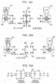
- Fig. 14A illustrates a relationship in terms of impedance between units in the configuration shown in Fig. 13 .
- Fig. 14B illustrates a relationship in terms of impedance between units for a case where the dielectric material 320 is removed from the configuration shown in Fig. 13 and the distance between the electrodes is increased.
- the impedance between the electrode has a small value, for example, several ⁇ .
- the impedance Z2 and the impedance Z3 on the electrode side become too large compared with the impedance Z1 of the power transmission circuit 110 and the impedance Z4 (for example, several ⁇ ) of the power reception circuit, and thus it becomes difficult to achieve impedance matching. As a result, it becomes impossible to achieve a high electric power transmission efficiency.
- each of the power transmission apparatus 100 and the power reception apparatus 200 has a combination of two parallel resonance circuits.
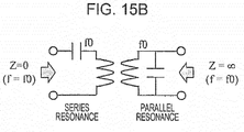
- the inventors of the present application have found that it is possible to solve the problem described above by configuring at least one of the power transmission apparatus 100 and the power reception apparatus 200 such that the two resonance circuits thereof are formed so as to have a combination of a series resonance circuit and a parallel resonance circuit. This configuration is described below with reference to Fig. 15A and Fig. 15B .
- Fig. 15A illustrates a resonator configuration in the known conventional power transmission apparatus 100.
- Fig. 15B illustrates a configuration obtained by replacing the resonance circuit on the power-supply side (left side in Fig. 15A ) in the configuration shown in Fig. 15A by a series resonance circuit.
- the resonators located on both the power-supply side and the electrode side are configured in the parallel resonance circuit, and thus both resonators have infinite impedance in the resonant state (in which the frequency f becomes equal to the resonance frequency f0). Therefore, it is difficult to achieve impedance matching between the low impedance on the power-supply side and the high impedance on the electrode side.
- the resonance circuit on the power-supply side is formed in the series resonance circuit, and thus it is possible to achieve impedance matching between the low impedance on the power-supply side and the high impedance on the electrode side.
- the impedance becomes zero (0) in the resonant state, and thus the series resonance circuit is suitable for achieving matching with low impedance.
- the parallel resonance circuit the impedance becomes infinite in the resonant state, and thus the parallel resonance circuit is suitable for achieving matching with high impedance.
- it is possible to easily achieve impedance matching by disposing a series resonance circuit on the power-supply side with low impedance and a parallel resonance circuit on the electrode side with high impedance as in the configuration shown in Fig. 15B .
- the technique described above can be applied not only to the power transmission apparatus 100 but also to the power reception apparatus 200. That is, it is possible to preferably achieve impedance matching in the power reception apparatus 200 by disposing a parallel resonance circuit on the electrode side and a series resonance circuit on the load side.
- the present disclosure provides a wireless power transmission system including a power transmission apparatus and a power reception apparatus, the power transmission apparatus including:
- the wireless power transmission system has at least one of the following combinations:
- a parallel resonance circuit is disposed on a side close to electrodes at least in one of the power transmission apparatus and the power reception apparatus, and a series resonance circuit is disposed on a side far from the electrodes. This makes it possible to preferably achieve impedance matching even in a case where the impedance between electrodes is high.
- Fig. 1 is a diagram schematically illustrating a wireless power transmission system according to the present embodiment.
- electric power is wirelessly transmitted from a power transmission apparatus having a pair of power transmission electrodes 120 embedded below a floor surface 30 to a transport robot 10 having a pair of power reception electrodes.
- the wireless power transmission is performed using the electric field coupling technique described above.
- the pair of power transmission electrodes 120 extends in parallel along the floor surface 30 over which the transport robot 10 is capable of conveying an object while receiving electric power.
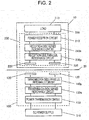
- Fig. 2 is a block diagram illustrating an outline of a configuration of the wireless power transmission system according to the present embodiment.
- This system includes a power transmission apparatus 100, and a transport robot 10.
- the power transmission apparatus 100 includes a power transmission circuit 110 that converts DC power supplied from an external DC power supply 310 to AC power, a transmission-side series resonance circuit 130s connected to the power transmission circuit 110, a transmission-side parallel resonance circuit 140p inductive coupled with the transmission-side series resonance circuit 130s, and two power transmission electrodes 120 that are connected to the transmission-side parallel resonance circuit 140p and transmit AC power.
- the transport robot 10 includes a power reception apparatus 200 and a load 330.
- the power reception apparatus 200 includes two power reception electrodes 220 that are capacitively coupled with the two power transmission electrodes 120 and contactlessly receive the transmitted AC power, a reception-side parallel resonance circuit 230p connected to the two power reception electrodes 220, a reception-side series resonance circuit 240s inductively coupled with the reception-side parallel resonance circuit 230p, and a power reception circuit 210 that are connected to the reception-side series resonance circuit 240s and that converts the received AC power to DC power and outputs the resultant DC power.
- the load 330 includes, for example, a secondary battery and a motor, and is charged or driven by the DC power output from the power reception circuit 210.
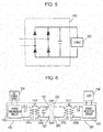
- Fig. 3 is a circuit diagram illustrating an outline of a configuration of the wireless power transmission system according to the present embodiment.
- the transmission-side series resonance circuit 130s in the power transmission apparatus 100 is configured such that a first coil L1 and a first capacitor C1 are connected in series.
- the transmission-side parallel resonance circuit 140p in the power transmission apparatus 100 is configured such that a second coil L2 and a second capacitor C2 are connected in parallel.
- the first coil L1 and the second coil L2 from a transformer in which the coil L1 and the coil L2 are coupled to each other with a coupling coefficient k1.
- the turn ratio (1 : N1) between the first coil L1 and the second coil L2 is set to a value so as to achieve a desired voltage transformation ratio.
- the reception-side parallel resonance circuit 230p in the power reception apparatus 200 is configured such that a third coil L3 and a third capacitor C3 are connected in parallel.
- the reception-side series resonance circuit 240s in the power reception apparatus 200 is configured such that a fourth coil L4 and a fourth capacitor C4 are connected in series.
- the third coil and the fourth coil from a transformer in which the coil L3 and the coil L4 are coupled to each other with a coupling coefficient k2.
- the turn ratio (N2 : 1) between the third coil L3 and the fourth coil L4 is set to a value so as to achieve a desired voltage transformation ratio (a step-up ratio or a step-down ratio).
- the wireless power transmission system includes both of the following combinations: the combination of transmission-side series resonance circuit 130s and the transmission-side parallel resonance circuit 140p, and the combination of the reception-side parallel resonance circuit 230p and the reception-side series resonance circuit 240s.
- reference symbols L1, L2, L3, and L4 used to denote inductors are also used to denote inductance values of the corresponding inductors.
- reference symbols C1, C2, C3, and C4 used to denote capacitors are also used to denote capacitance values of the corresponding capacitors.
- Fig. 4 is a diagram schematically illustrating an example of a configuration of the power transmission circuit 110.
- the power transmission circuit 110 includes a full-bridge inverter circuit including four switching elements (for example, transistors such as IGBTs, MOSFETs, or the like) and a control circuit 112.
- the control circuit 112 includes a gate driver that outputs a control signal to control an on-state (conduction state) and an off-state (non-conduction state) of each switching element, and a processor such as a microcontroller or the like for controlling the gate driver to output the control signal.
- the power transmission circuit 110 may include a modulation-demodulation circuit for communication, and various sensors for measuring a voltage, a current, or the like.
- Fig. 5 is a diagram schematically illustrating an example of a configuration of the power reception circuit 210.
- the power reception circuit 210 is a full-wave rectifying circuit including a diode bride and a smoothing capacitor.
- the power reception circuit 210 may be configured in the form of another type of rectifier.
- the power reception circuit 210 may include, in addition to the rectification circuit, other various circuits such as a constant voltage/constant current control circuit, a modulation-demodulation circuit for communication, or the like.
- the power reception circuit 210 converts the received AC energy to DC energy usable by the load 330.
- the power reception circuit 210 may further include various sensors for measuring a voltage, a current, or the like output from the reception-side series resonance circuit 240s.
- each coil used therein may be, for example, a planar coil or a multilayer coil formed on a circuit board, or a winding coil using a copper wire, a litz wire, or a twisted wire.
- each capacitor may be a capacitor of any type, for example, a capacitor having a chip shape or a lead shape. Capacitance formed between two wirings via air may be used as each capacitor. Instead of using capacitors, a self-resonance characteristic possessed by each coil may be used.
- the DC power supply 310 may be an arbitrary power supply such as a commercial power supply, a primary battery, a secondary battery, a solar battery, a fuel battery, a USB (Universal Serial Bus) power supply, a high-capacitance capacitor (for example, an electric double-layer capacitor), a voltage transformer connected to a commercial power supply, or the like.
- a commercial power supply such as a commercial power supply, a primary battery, a secondary battery, a solar battery, a fuel battery, a USB (Universal Serial Bus) power supply, a high-capacitance capacitor (for example, an electric double-layer capacitor), a voltage transformer connected to a commercial power supply, or the like.
- the resonance frequency f0 of each of the transmission-side series resonance circuit 130s, the transmission-side parallel resonance circuit 140p, the reception-side parallel resonance circuit 230p, and the reception-side series resonance circuit 240s does not need to be exactly equal to the transmission frequency f0.
- Each resonance frequency f0 may be set, for example, in a range of 50% to 150% of the transmission frequency f.
- the frequency f in the electric power transmission may be set, for example, in a range from 50 Hz to 300 GHz and more preferably from 20 kHz to 10 GHz, still more preferably from 20 kHz to 20 MHz, and still more preferably from 20 kHz to 1 MHz.
- the distance between the power transmission electrode 120 and the power reception electrode 220 there is an air gap between the power transmission electrode 120 and the power reception electrode 220, and the distance between them is set to be relatively large (for example, about 10 mm). Therefore, the capacitance Cm1 and the capacitance Cm2 between the electrodes are very small, and the impedance of the power transmission electrode 120 and the impedance of the power reception electrode 220 is very high (for example, about several k ⁇ ). In contrast, the impedances of the power transmission circuit 110 and the power reception circuit 210 are as small as, for example, several ⁇ .
- the transmission-side parallel resonance circuit 140p and the reception-side parallel resonance circuit 230p are respectively disposed on sides close to the power transmission electrode 120 and the power reception electrode 220, and the transmission-side series resonance circuit 130s and the reception-side series resonance circuit 240s are respectively disposed on sides close to the power transmission circuit 110 and the power reception circuit 210.
- This configuration makes it possible to easily achieve the impedance matching. As a result, it becomes possible to transmit electric power with a higher efficiency than is conventionally achieved as described later.
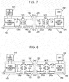
- Fig. 6 is a circuit diagram illustrating an outline of a configuration of the wireless power transmission system according to the present embodiment.
- the present embodiment is different from the first embodiment in that the power reception apparatus 200 includes a circuit 230c including a third coil L3 instead of the reception-side parallel resonance circuit 230p in the first embodiment.
- the inductance value L4 of the fourth coil L4 is smaller than the inductance value L3 of the third coil L3.
- the present embodiment is similar to the first embodiment.
- the power transmission apparatus 100 has a combination of i) a transmission-side series resonance circuit 130s including a first coil and a first capacitor disposed between the first coil and a power transmission circuit 110, and ii) a transmission-side parallel resonance circuit 140p including a second coil and a second capacitor disposed between the second coil and two power transmission electrodes 120.
- the power reception apparatus 200 has a combination of i) the third coil with the inductance value L3 and ii) a reception-side series resonance circuit 240s including a fourth coil with an inductance value L4 lower than the inductance value L3 and a fourth capacitor disposed between the fourth coil and the power reception circuit 210.
- the power transmission apparatus 100 has a combination of a series resonance circuit and a parallel resonance circuit although the power reception apparatus 200 does not have a combination of a series resonance circuit and a parallel resonance circuit.
- This configuration makes it possible to easily achieve impedance matching in the power transmission apparatus 100.
- Fig. 7 is a circuit diagram illustrating an outline of a configuration of the wireless power transmission system according to the present embodiment.
- the present embodiment is different from the first embodiment in that the power transmission apparatus 100 includes a circuit 140c including a second coil L2 instead of the transmission-side parallel resonance circuit 140p in the first embodiment.
- the inductance value L2 of the second coil L2 is greater than the inductance value L1 of the first coil L1.
- the present embodiment is similar to the first embodiment.
- the power transmission apparatus 100 has a combination of i) a transmission-side series resonance circuit 130s including the first coil with the inductance value L1 and a first capacitor disposed between the first coil and a power transmission circuit 110, and ii) the second coil with the inductance value L2 higher than the inductance value L1.
- the power reception apparatus 200 has a combination of i) a reception-side parallel resonance circuit 230p including a third coil and a third capacitor disposed between the third coil and two power reception electrodes 220, and ii) a reception-side series resonance circuit 240s including the fourth coil and a fourth capacitor disposed between the fourth coil and a power reception circuit 210.
- the power reception apparatus 200 has a combination of a series resonance circuit and a parallel resonance circuit although the power transmission apparatus 100 does not have a combination of a series resonance circuit and a parallel resonance circuit.
- This configuration makes it possible to easily achieve impedance matching in the power reception apparatus 200.
- Fig. 8 is a circuit diagram illustrating an outline of a configuration of the wireless power transmission system according to the present embodiment.
- the present embodiment is different from the first embodiment in that the power transmission apparatus 100 includes a parallel resonance circuit 130p instead of the transmission-side series resonance circuit 130s in the first embodiment. Except for the above, the present embodiment is similar to the first embodiment.
- the power reception apparatus 200 has a combination of a series resonance circuit and a parallel resonance circuit although the power transmission apparatus 100 does not have a combination of a series resonance circuit and a parallel resonance circuit.
- This configuration makes it possible to easily achieve impedance matching in the power reception apparatus 200.
- Fig. 9 is a circuit diagram illustrating an outline of a configuration of the wireless power transmission system according to the present embodiment.
- the present embodiment is different from the first embodiment in that the power reception apparatus 200 includes a reception-side parallel resonance circuit 230p instead of the reception-side series resonance circuit 240s in the first embodiment. Except for the above, the present embodiment is similar to the first embodiment.
- the power transmission apparatus 100 has a combination of a series resonance circuit and a parallel resonance circuit although the power reception apparatus 200 does not have a combination of a series resonance circuit and a parallel resonance circuit.
- This configuration makes it possible to easily achieve impedance matching in the power transmission apparatus 100.
- the inventors of the present disclosure performed circuit simulations for wireless power transmission systems configured according to the first to fifth embodiments, and made comparisons with the configuration of the comparative example shown in Fig. 13 thereby verifying the advantageous effects of the embodiments of the present disclosure.
- Fig. 10 is a diagram schematically illustrating a positional relationship between a pair of power transmission electrodes 120 and a pair of power reception electrodes 220 in an example and the comparative example.
- the two power transmission electrodes 120 are disposed in parallel via a gap of 100 mm, and the two power reception electrodes 220 are disposed opposing the two power transmission electrodes 120.
- the size of each power transmission electrode 120 was set to 100 mm 2 ⁇ 1000 mm 2
- the size of each power reception electrode 220 was set to 100 mm ⁇ 400 mm 2 .
- the distance between the power transmission electrode 120 and the power reception electrode 220 was set to 10 mm.
- Fig. 11 is a diagram illustrating an equivalent circuit of the power transmission electrodes 120 and the power reception electrodes 220.
- Cm1 and Cm2 denote the capacitances of two capacitors formed by the two power transmission electrodes 120 and the two power reception electrodes 220.
- C22 denote the capacitance between the two power transmission electrodes 120
- C33 denote the capacitance between the two power reception electrodes 220.
- C2 or C3 may be omitted.
- the inductance value L2 of the second coil and the inductance value L3 of the third coil were both set to 100 ⁇ H.
- the Q-value of a matching transformer formed by a combination of a series resonance circuit and a parallel resonance circuit was to 300.
- the ratio, L2/L1, of the inductance value L2 of the second coil to the inductance value L1 of the first coil is denoted by an inductance ratio N1.
- the ratio, L3/L4, of the inductance value L3 of the third coil to the inductance value L4 of the fourth coil is denoted by an inductance ratio N2.
- the inductance ratio equal to a turn ratio.
- the transmission frequency f was set to 480 kHz.
- each coil a spiral coil with a diameter of 80 mm was used which was formed in two layers using a litz wire including 375 element wires each having a diameter of 40 ⁇ m.
- a magnetic shield was disposed at each location 20 mm above and 20 mm below each coil.
- the inductance L2 of the second coil and the inductance L3 of the third coil on the high-impedance side were fixed to 100 ⁇ H, and the inductance L1 of the first coil and the inductance L4 of the fourth coil on the low-impedance side were adjusted so as to achieve as good impedance matching as possible.
- Table 1 shows the inductance ratios (turn ratios) N1 and N2, the coupling coefficients k1 and k2, and electric power transmission efficiencies for the configurations according to the first to fifth embodiments and the comparative example.
- Table 2 shows capacitance values C1 to C4 for the respective configurations.
- each parameter shown in Tables 1 and 2 was set in each configuration so as to minimize the reduction in efficiency caused by impedance mismatching.
- Table 1 in the configurations having at least one combination of a series resonance circuit and a parallel resonance circuit according to the first to fifth embodiments, it has been confirmed that a higher efficiency is achieved than is achieved in the configuration of the comparative example.
- the turn ratios N1 and N2 were set to as very large a value as 20. Such a large turn ratio is not usually used because a reduction in Q-value occurs.
- impedance matching is not achieved, which results in a further reduction in transmission efficiency from the values shown in Table 1.
- the effects of the embodiments of the present disclosure are greater as the impedance between the two power transmission electrodes 120 and the two power reception electrodes 220 increases.
- the capacitance between the electrodes is denoted by C and the angular frequency of the transmitted electric power is denoted by ⁇
- the impedance between the electrodes is represented as 1/( ⁇ C), where the capacitance between the electrodes is one of the capacitance Cm1 and the capacitance Cm2 or the average value thereof.
- the impedance between the electrodes is higher, for example, than the impedance ⁇ L2 of the second coil, it is possible to achieve further enhanced effects in the embodiments of the present disclosure. Therefore, it is preferable to satisfy ⁇ L2 ⁇ 1/( ⁇ C). More preferably, each constituent element is designed such that 10 ⁇ L2 ⁇ 1/( ⁇ C) is satisfied.
- the Q-value is an index indicating the degree to which the loss is low. The loss decreases as the Q-value increases. Therefore, it is desirable to set the Q-value of the matching transformer to be as high as possible.
- Fig. 12 is a graph representing a relationship between the inductance ratio N and the Q-value of the matching transformer.
- the Q-value of the coil (the second coil or the third coil) on the high-impedance side is denoted by QLhi
- the Q-value of the coil (the first coil or the fourth coil) on the low-impedance side is denoted by QLlo
- the Q-value of the matching transformer is represented as ⁇ (QLhi * QLlo).
- the inductance Lhi of the coil on the high-impedance side was fixed to 100 ⁇ H, and the number of turns of the coil on the low-impedance side was changed within a range from 3 to 50 thereby changing the impedance ratio N.
- the inductance ratio N that is, the ratio of the inductance value L2 to the inductance value L1 or the ratio of the inductance value L3 to the inductance value L4 is designed such that 1 ⁇ N ⁇ 15 is preferably satisfied, and more preferably 3 ⁇ N ⁇ 8 is satisfied.
- the present disclosure includes wireless power transmission systems and power transmission apparatuses described below in the following items.
- a wireless power transmission system includes a power transmission apparatus and a power reception apparatus, the power transmission apparatus including a power transmission circuit that converts DC power of an external DC power supply to AC power, a first coil connected to the power transmission circuit, a second coil inductively coupled to the first coil, and two power transmission electrodes that are connected to the second coil and that transmit the AC power, the power reception apparatus including two power reception electrodes disposed opposing the two power transmission electrodes so as to be capacitively coupled with the two power transmission electrodes to contactlessly receive the transmitted AC power, a third coil connected to the two power reception electrodes, a fourth coil connected to the third coil, and a power reception circuit that is connected to the fourth coil and that converts the received AC power to DC power, the wireless power transmission system having at least one of the following combinations:
- the wireless power transmission system has at least one of the following combinations:
- a parallel resonance circuit is disposed on a side close to an electrode, and a series resonance circuit is disposed on a side far from the electrode, and thus it is possible to preferably achieve impedance matching even in a case where the impedance between electrodes is high.
- the wireless power transmission system described in item 1 may have a combination of
- a parallel resonance circuit is disposed on a side close to an electrode, and a series resonance circuit is disposed on a side far from electrodes, and thus it is possible to more preferably achieve impedance matching.
- the wireless power transmission system described in item 1 may have a combination of
- a parallel resonance circuit is disposed on a side close to an electrode, and a series resonance circuit is disposed on a side far from electrodes.
- impedance matching it is possible to preferably achieve impedance matching.
- the wireless power transmission system described in item 1 may have a combination of
- a parallel resonance circuit is disposed on a side close to an electrode, and a series resonance circuit is disposed on a side far from electrodes.
- impedance matching it is possible to preferably achieve impedance matching.
- an air gap may be provided between the two power transmission electrodes and the two power reception electrodes disposed opposing the two power transmission electrodes.
- the electrodes are spaced apart via the air gap, and it is not necessary to provide a dielectric material with high relative permittivity, which makes it possible to simplify the configuration between electrodes.
- the impedance between the electrodes is higher than the impedance of the second coil, and thus it is possible to achieve further enhanced effects of the impedance matching.
- the impedance between the electrodes is extremely higher than the impedance of the second coil, and thus it is possible to achieve further extremely enhanced effects of the impedance matching.
- the Q-value being as high as, for example, 70% or more of the peak value.
- the Q-value being as high as, for example, 90% or more of the peak value.
- the Q-value being as high as, for example, 70% or more of the peak value.
- the Q-value being as high as, for example, 90% or more of the peak value.
- a power transmission apparatus in a wireless power transmission system includes the power transmission apparatus and a power reception apparatus, the power transmission apparatus including a power transmission circuit that converts DC power of an external DC power supply to AC power, a first coil connected to the power transmission circuit, a second coil inductively coupled to the first coil, two power transmission electrodes that are connected to the second coil and that transmit the AC power, the power reception apparatus including two power reception electrodes disposed opposing the two power transmission electrodes so as to be capacitively coupled with the two power transmission electrodes to contactlessly receive the transmitted AC power, a third coil connected to the two power reception electrodes, a fourth coil connected to the third coil, and a power reception circuit that is connected to the fourth coil and that converts the received AC power to DC power, the power transmission apparatus having a combination of a transmission-side series resonance circuit including the first coil and a first capacitor disposed between the first coil and the power transmission circuit, and a transmission-side parallel resonance circuit including the second coil and a second capacitor disposed between the second coil and the two power transmission electrodes.
- the power transmission apparatus has the combination of the transmission-side series resonance circuit including the first coil and the first capacitor disposed between the first coil and the power transmission circuit, and the transmission-side parallel resonance circuit including the second coil and the second capacitor disposed between the second coil and the two power transmission electrodes.
- a parallel resonance circuit is disposed on a side close to an electrode, and a series resonance circuit is disposed on a side far from the electrode. This makes it possible to advantageously achieve impedance matching even in a case where the impedance between electrodes is high.
- an air gap may be provided between the two power transmission electrodes and the two power reception electrodes disposed opposing the two power transmission electrodes.
- the electrodes are spaced apart via the air gap, and it is not necessary to provide a dielectric material with high relative permittivity, which makes it possible to simplify the configuration between electrodes.
- the impedance between the electrodes is higher than the impedance of the second coil, and thus it is possible to achieve further enhanced effects of the impedance matching.
- the impedance between the electrodes is extremely higher than the impedance of the second coil, and thus it is possible to achieve further extremely enhanced effects of the impedance matching.
- the Q-value being as high as, for example, 70% or more of the peak value.
- the Q-value being as high as, for example, 90% or more of the peak value.
- the technique of the present disclosure may be used in an apparatus such as a surveillance camera, a robot, or the like in which, in addition to electric power transmission, real-time bidirectional transmission of data is necessary. According to embodiments of the present disclosure, it is possible to perform full-duplex bidirectional data transmission between a power transmission apparatus and a power reception apparatus.
Landscapes
- Engineering & Computer Science (AREA)
- Power Engineering (AREA)
- Computer Networks & Wireless Communication (AREA)
- Signal Processing (AREA)
- Charge And Discharge Circuits For Batteries Or The Like (AREA)
Applications Claiming Priority (2)
| Application Number | Priority Date | Filing Date | Title |
|---|---|---|---|
| JP2015191406A JP6618006B2 (ja) | 2015-09-29 | 2015-09-29 | 無線電力伝送システムおよび送電装置 |
| PCT/JP2016/000518 WO2017056343A1 (fr) | 2015-09-29 | 2016-02-02 | Système de transmission d'énergie sans fil et dispositif de transmission d'énergie |
Publications (3)
| Publication Number | Publication Date |
|---|---|
| EP3358709A1 true EP3358709A1 (fr) | 2018-08-08 |
| EP3358709A4 EP3358709A4 (fr) | 2018-08-29 |
| EP3358709B1 EP3358709B1 (fr) | 2021-11-03 |
Family
ID=58423205
Family Applications (1)
| Application Number | Title | Priority Date | Filing Date |
|---|---|---|---|
| EP16850530.3A Active EP3358709B1 (fr) | 2015-09-29 | 2016-02-02 | Système de transmission d'énergie sans fil et dispositif de transmission d'énergie |
Country Status (5)
| Country | Link |
|---|---|
| US (1) | US10432022B2 (fr) |
| EP (1) | EP3358709B1 (fr) |
| JP (1) | JP6618006B2 (fr) |
| CN (1) | CN107078545B (fr) |
| WO (1) | WO2017056343A1 (fr) |
Families Citing this family (10)
| Publication number | Priority date | Publication date | Assignee | Title |
|---|---|---|---|---|
| KR20170110866A (ko) * | 2016-03-24 | 2017-10-12 | 현대자동차주식회사 | 무선 전력 전송 일차 코일 회로 및 이를 이용하는 그라운드 어셈블리와 그 제조 방법 |
| US10819152B2 (en) * | 2016-09-12 | 2020-10-27 | The Research Foundation For The State University Of New York | Wireless power transfer systems and components thereof |
| JP2019009981A (ja) * | 2017-06-21 | 2019-01-17 | パナソニックIpマネジメント株式会社 | 無線電力伝送システム、送電装置、および受電装置 |
| JP7054834B2 (ja) * | 2017-07-20 | 2022-04-15 | パナソニックIpマネジメント株式会社 | 電極ユニット、送電装置、受電装置、電子機器、移動体、および無線電力伝送システム |
| JP7067174B2 (ja) * | 2018-03-22 | 2022-05-16 | スミダコーポレーション株式会社 | 共振整合回路 |
| CN111971872A (zh) * | 2018-03-28 | 2020-11-20 | 松下知识产权经营株式会社 | 电极组件、送电装置、受电装置以及无线电力传输系统 |
| EP3780335A4 (fr) * | 2018-03-28 | 2021-05-19 | Panasonic Intellectual Property Management Co., Ltd. | Module de transmission de courant, module de réception de courant, dispositif de transmission de courant, dispositif de réception de courant et système de transfert de courant sans fil |
| CN109274183B (zh) * | 2018-11-09 | 2022-03-04 | 西南交通大学 | 一种具有高抗偏移特性的无线电能传输系统 |
| JP7518510B2 (ja) * | 2020-10-23 | 2024-07-18 | 株式会社ExH | 電力供給システム |
| KR102943219B1 (ko) * | 2020-12-07 | 2026-03-25 | 삼성전자주식회사 | 무선 전력 수신기 및 무선 전력기를 포함하는 무선 전력 전송 시스템 |
Family Cites Families (22)
| Publication number | Priority date | Publication date | Assignee | Title |
|---|---|---|---|---|
| KR100853889B1 (ko) * | 2005-07-29 | 2008-08-25 | 엘에스전선 주식회사 | 무 접점 충전 배터리 및 충전기, 이들을 포함하는 배터리충전 세트, 및 충전제어 방법 |
| US7511502B2 (en) * | 2007-01-05 | 2009-03-31 | Kabushiki Kaisha Toshiba | Magnetic resonance imaging apparatus |
| JP5415780B2 (ja) | 2009-02-20 | 2014-02-12 | 健一 原川 | 電力供給システム、及びそのための可動体と固定体 |
| EP2443724B8 (fr) * | 2009-08-13 | 2013-01-16 | Panasonic Corporation | Unité de transmission d'énergie sans fil, générateur d'énergie et système de génération d'énergie comprenant l'unité |
| US8482250B2 (en) * | 2010-08-06 | 2013-07-09 | Cynetic Designs Ltd. | Inductive transmission of power and data through ceramic armor panels |
| JP5354097B2 (ja) * | 2011-05-13 | 2013-11-27 | 株式会社村田製作所 | 電力送電装置、電力受電装置および電力伝送システム |
| US9099885B2 (en) * | 2011-06-17 | 2015-08-04 | Semiconductor Energy Laboratory Co., Ltd. | Wireless power feeding system |
| JP6118320B2 (ja) * | 2011-08-16 | 2017-04-19 | フィリップス ライティング ホールディング ビー ヴィ | 容量性電力伝送を用いた配電のための広表面導電層 |
| US20150326028A1 (en) * | 2011-09-21 | 2015-11-12 | Pioneer Corporation | Wireless power transmitting apparatus, wireless power receiving apparatus, and wireless power feeding system |
| WO2013105279A1 (fr) * | 2012-01-12 | 2013-07-18 | 富士通株式会社 | Dispositif de transmission de puissance et système de réception de puissance |
| EP2674950A1 (fr) * | 2012-06-11 | 2013-12-18 | Tyco Electronics Nederland B.V. | Connecteur sans contact, système de connecteur sans contact et procédé de fabrication du connecteur sans contact |
| US9444270B2 (en) * | 2012-08-02 | 2016-09-13 | Sandisk Technologies Llc | Wireless power transfer |
| JP5643270B2 (ja) * | 2012-09-13 | 2014-12-17 | トヨタ自動車株式会社 | 車両および非接触給電システム |
| JP6088814B2 (ja) * | 2012-12-17 | 2017-03-01 | 古河電気工業株式会社 | 無線電力伝送システム |
| WO2014103438A1 (fr) | 2012-12-28 | 2014-07-03 | 株式会社村田製作所 | Système de transmission de puissance |
| JPWO2014208683A1 (ja) * | 2013-06-27 | 2017-02-23 | 昭和電工株式会社 | 電力伝送体、電力供給装置、電力消費装置、電力供給システムおよび電力伝送体の製造方法 |
| JP5862844B2 (ja) * | 2013-10-09 | 2016-02-16 | 株式会社村田製作所 | ワイヤレス電力伝送システム |
| JP6167877B2 (ja) * | 2013-11-29 | 2017-07-26 | 株式会社デンソー | 非接触給電システム |
| JP6274504B2 (ja) * | 2013-11-29 | 2018-02-07 | 日産自動車株式会社 | 電池システム |
| JP2016010284A (ja) * | 2014-06-26 | 2016-01-18 | 株式会社豊田自動織機 | 送電機器及び非接触電力伝送装置 |
| US9837847B2 (en) * | 2014-10-28 | 2017-12-05 | Lite-On Technology Corporation | Wireless charging transmitter and method thereof |
| WO2016151889A1 (fr) * | 2015-03-23 | 2016-09-29 | 三菱電機株式会社 | Dispositif d'alimentation électrique sans contact bidirectionnel et système d'alimentation électrique sans contact bidirectionnel |
-
2015
- 2015-09-29 JP JP2015191406A patent/JP6618006B2/ja active Active
-
2016
- 2016-02-02 WO PCT/JP2016/000518 patent/WO2017056343A1/fr not_active Ceased
- 2016-02-02 CN CN201680003273.9A patent/CN107078545B/zh active Active
- 2016-02-02 EP EP16850530.3A patent/EP3358709B1/fr active Active
-
2017
- 2017-07-07 US US15/643,507 patent/US10432022B2/en active Active
Also Published As
| Publication number | Publication date |
|---|---|
| EP3358709B1 (fr) | 2021-11-03 |
| US20170310162A1 (en) | 2017-10-26 |
| EP3358709A4 (fr) | 2018-08-29 |
| JP2017070055A (ja) | 2017-04-06 |
| JP6618006B2 (ja) | 2019-12-11 |
| CN107078545A (zh) | 2017-08-18 |
| WO2017056343A1 (fr) | 2017-04-06 |
| US10432022B2 (en) | 2019-10-01 |
| CN107078545B (zh) | 2021-06-11 |
Similar Documents
| Publication | Publication Date | Title |
|---|---|---|
| EP3358709B1 (fr) | Système de transmission d'énergie sans fil et dispositif de transmission d'énergie | |
| US9893567B2 (en) | Dual-mode wireless power transfer apparatus | |
| US9088307B2 (en) | Non-resonant and quasi-resonant system for wireless power transmission to multiple receivers | |
| CN102918748B (zh) | 无线电力传输装置 | |
| KR101478930B1 (ko) | 비접촉 급전 장치 | |
| US10153664B2 (en) | Wireless power transmission system and power transmitter | |
| US10158254B2 (en) | Resonant coupling power transmission system, resonance type power transmission device, and resonance type power reception device | |
| EP3016232A1 (fr) | Dispositif de transmission d'énergie, véhicule équipé d'un dispositif de transmission d'énergie et système de transmission d'énergie sans fil | |
| CA3150958A1 (fr) | Systeme de transfert d'energie sans fil haute frequence, emetteur et recepteur associes | |
| CN106560976A (zh) | 无线充电发射系统和无线充电接收系统 | |
| JP6535003B2 (ja) | 無線電力受信装置 | |
| US20170366047A1 (en) | Wireless power transmission apparatus for performing non-contact transmission by electromagnetic induction | |
| WO2012172900A1 (fr) | Système d'alimentation électrique sans contact de type résonance | |
| CN109103996A (zh) | 无线电力传输系统、送电装置以及受电装置 | |
| CN111971872A (zh) | 电极组件、送电装置、受电装置以及无线电力传输系统 | |
| JP6817604B2 (ja) | 送電装置および無線電力伝送システム | |
| JP6835082B2 (ja) | 電力変換装置 | |
| CN107346918A (zh) | 一种无线电能传输装置 | |
| CN205921458U (zh) | 无线充电发射系统和无线充电接收系统 | |
| CN110445259A (zh) | 一种基于多发射无线电能传输系统的效率提升方法 | |
| US10491043B2 (en) | Resonant coil, wireless power transmitter using the same, wireless power receiver using the same | |
| KR101905882B1 (ko) | 무선전력 송신장치, 무선전력 수신장치, 무선전력 전송 시스템 및 무선전력 전송 방법 | |
| CN107658994A (zh) | 一种无线电能传输系统 | |
| Thoen et al. | Design of an inductively coupled wireless power system for moving receivers | |
| US20140054972A1 (en) | Wireless power transmission system |
Legal Events
| Date | Code | Title | Description |
|---|---|---|---|
| STAA | Information on the status of an ep patent application or granted ep patent |
Free format text: STATUS: THE INTERNATIONAL PUBLICATION HAS BEEN MADE |
|
| PUAI | Public reference made under article 153(3) epc to a published international application that has entered the european phase |
Free format text: ORIGINAL CODE: 0009012 |
|
| STAA | Information on the status of an ep patent application or granted ep patent |
Free format text: STATUS: REQUEST FOR EXAMINATION WAS MADE |
|
| 17P | Request for examination filed |
Effective date: 20180222 |
|
| AK | Designated contracting states |
Kind code of ref document: A1 Designated state(s): AL AT BE BG CH CY CZ DE DK EE ES FI FR GB GR HR HU IE IS IT LI LT LU LV MC MK MT NL NO PL PT RO RS SE SI SK SM TR |
|
| AX | Request for extension of the european patent |
Extension state: BA ME |
|
| A4 | Supplementary search report drawn up and despatched |
Effective date: 20180731 |
|
| RIC1 | Information provided on ipc code assigned before grant |
Ipc: H04B 5/00 20060101ALI20180725BHEP Ipc: H02M 3/335 20060101ALI20180725BHEP Ipc: H02J 7/02 20160101ALI20180725BHEP Ipc: H02J 50/05 20160101AFI20180725BHEP |
|
| DAV | Request for validation of the european patent (deleted) | ||
| DAX | Request for extension of the european patent (deleted) | ||
| STAA | Information on the status of an ep patent application or granted ep patent |
Free format text: STATUS: EXAMINATION IS IN PROGRESS |
|
| 17Q | First examination report despatched |
Effective date: 20190729 |
|
| REG | Reference to a national code |
Ref country code: DE Ref legal event code: R079 Ref document number: 602016065839 Country of ref document: DE Free format text: PREVIOUS MAIN CLASS: H02J0050000000 Ipc: H02J0007000000 |
|
| GRAP | Despatch of communication of intention to grant a patent |
Free format text: ORIGINAL CODE: EPIDOSNIGR1 |
|
| STAA | Information on the status of an ep patent application or granted ep patent |
Free format text: STATUS: GRANT OF PATENT IS INTENDED |
|
| RIC1 | Information provided on ipc code assigned before grant |
Ipc: H04B 5/00 20060101ALI20210613BHEP Ipc: H02J 50/05 20160101ALI20210613BHEP Ipc: H02M 3/335 20060101ALI20210613BHEP Ipc: H02J 7/00 20060101AFI20210613BHEP |
|
| INTG | Intention to grant announced |
Effective date: 20210708 |
|
| GRAS | Grant fee paid |
Free format text: ORIGINAL CODE: EPIDOSNIGR3 |
|
| GRAA | (expected) grant |
Free format text: ORIGINAL CODE: 0009210 |
|
| STAA | Information on the status of an ep patent application or granted ep patent |
Free format text: STATUS: THE PATENT HAS BEEN GRANTED |
|
| AK | Designated contracting states |
Kind code of ref document: B1 Designated state(s): AL AT BE BG CH CY CZ DE DK EE ES FI FR GB GR HR HU IE IS IT LI LT LU LV MC MK MT NL NO PL PT RO RS SE SI SK SM TR |
|
| REG | Reference to a national code |
Ref country code: GB Ref legal event code: FG4D |
|
| REG | Reference to a national code |
Ref country code: AT Ref legal event code: REF Ref document number: 1444859 Country of ref document: AT Kind code of ref document: T Effective date: 20211115 Ref country code: CH Ref legal event code: EP |
|
| REG | Reference to a national code |
Ref country code: DE Ref legal event code: R096 Ref document number: 602016065839 Country of ref document: DE |
|
| REG | Reference to a national code |
Ref country code: IE Ref legal event code: FG4D |
|
| REG | Reference to a national code |
Ref country code: LT Ref legal event code: MG9D |
|
| REG | Reference to a national code |
Ref country code: NL Ref legal event code: MP Effective date: 20211103 |
|
| REG | Reference to a national code |
Ref country code: AT Ref legal event code: MK05 Ref document number: 1444859 Country of ref document: AT Kind code of ref document: T Effective date: 20211103 |
|
| PG25 | Lapsed in a contracting state [announced via postgrant information from national office to epo] |
Ref country code: RS Free format text: LAPSE BECAUSE OF FAILURE TO SUBMIT A TRANSLATION OF THE DESCRIPTION OR TO PAY THE FEE WITHIN THE PRESCRIBED TIME-LIMIT Effective date: 20211103 Ref country code: LT Free format text: LAPSE BECAUSE OF FAILURE TO SUBMIT A TRANSLATION OF THE DESCRIPTION OR TO PAY THE FEE WITHIN THE PRESCRIBED TIME-LIMIT Effective date: 20211103 Ref country code: FI Free format text: LAPSE BECAUSE OF FAILURE TO SUBMIT A TRANSLATION OF THE DESCRIPTION OR TO PAY THE FEE WITHIN THE PRESCRIBED TIME-LIMIT Effective date: 20211103 Ref country code: BG Free format text: LAPSE BECAUSE OF FAILURE TO SUBMIT A TRANSLATION OF THE DESCRIPTION OR TO PAY THE FEE WITHIN THE PRESCRIBED TIME-LIMIT Effective date: 20220203 Ref country code: AT Free format text: LAPSE BECAUSE OF FAILURE TO SUBMIT A TRANSLATION OF THE DESCRIPTION OR TO PAY THE FEE WITHIN THE PRESCRIBED TIME-LIMIT Effective date: 20211103 |
|
| PG25 | Lapsed in a contracting state [announced via postgrant information from national office to epo] |
Ref country code: IS Free format text: LAPSE BECAUSE OF FAILURE TO SUBMIT A TRANSLATION OF THE DESCRIPTION OR TO PAY THE FEE WITHIN THE PRESCRIBED TIME-LIMIT Effective date: 20220303 Ref country code: SE Free format text: LAPSE BECAUSE OF FAILURE TO SUBMIT A TRANSLATION OF THE DESCRIPTION OR TO PAY THE FEE WITHIN THE PRESCRIBED TIME-LIMIT Effective date: 20211103 Ref country code: PT Free format text: LAPSE BECAUSE OF FAILURE TO SUBMIT A TRANSLATION OF THE DESCRIPTION OR TO PAY THE FEE WITHIN THE PRESCRIBED TIME-LIMIT Effective date: 20220303 Ref country code: PL Free format text: LAPSE BECAUSE OF FAILURE TO SUBMIT A TRANSLATION OF THE DESCRIPTION OR TO PAY THE FEE WITHIN THE PRESCRIBED TIME-LIMIT Effective date: 20211103 Ref country code: NO Free format text: LAPSE BECAUSE OF FAILURE TO SUBMIT A TRANSLATION OF THE DESCRIPTION OR TO PAY THE FEE WITHIN THE PRESCRIBED TIME-LIMIT Effective date: 20220203 Ref country code: NL Free format text: LAPSE BECAUSE OF FAILURE TO SUBMIT A TRANSLATION OF THE DESCRIPTION OR TO PAY THE FEE WITHIN THE PRESCRIBED TIME-LIMIT Effective date: 20211103 Ref country code: LV Free format text: LAPSE BECAUSE OF FAILURE TO SUBMIT A TRANSLATION OF THE DESCRIPTION OR TO PAY THE FEE WITHIN THE PRESCRIBED TIME-LIMIT Effective date: 20211103 Ref country code: HR Free format text: LAPSE BECAUSE OF FAILURE TO SUBMIT A TRANSLATION OF THE DESCRIPTION OR TO PAY THE FEE WITHIN THE PRESCRIBED TIME-LIMIT Effective date: 20211103 Ref country code: GR Free format text: LAPSE BECAUSE OF FAILURE TO SUBMIT A TRANSLATION OF THE DESCRIPTION OR TO PAY THE FEE WITHIN THE PRESCRIBED TIME-LIMIT Effective date: 20220204 Ref country code: ES Free format text: LAPSE BECAUSE OF FAILURE TO SUBMIT A TRANSLATION OF THE DESCRIPTION OR TO PAY THE FEE WITHIN THE PRESCRIBED TIME-LIMIT Effective date: 20211103 |
|
| PG25 | Lapsed in a contracting state [announced via postgrant information from national office to epo] |
Ref country code: SM Free format text: LAPSE BECAUSE OF FAILURE TO SUBMIT A TRANSLATION OF THE DESCRIPTION OR TO PAY THE FEE WITHIN THE PRESCRIBED TIME-LIMIT Effective date: 20211103 Ref country code: SK Free format text: LAPSE BECAUSE OF FAILURE TO SUBMIT A TRANSLATION OF THE DESCRIPTION OR TO PAY THE FEE WITHIN THE PRESCRIBED TIME-LIMIT Effective date: 20211103 Ref country code: RO Free format text: LAPSE BECAUSE OF FAILURE TO SUBMIT A TRANSLATION OF THE DESCRIPTION OR TO PAY THE FEE WITHIN THE PRESCRIBED TIME-LIMIT Effective date: 20211103 Ref country code: EE Free format text: LAPSE BECAUSE OF FAILURE TO SUBMIT A TRANSLATION OF THE DESCRIPTION OR TO PAY THE FEE WITHIN THE PRESCRIBED TIME-LIMIT Effective date: 20211103 Ref country code: DK Free format text: LAPSE BECAUSE OF FAILURE TO SUBMIT A TRANSLATION OF THE DESCRIPTION OR TO PAY THE FEE WITHIN THE PRESCRIBED TIME-LIMIT Effective date: 20211103 Ref country code: CZ Free format text: LAPSE BECAUSE OF FAILURE TO SUBMIT A TRANSLATION OF THE DESCRIPTION OR TO PAY THE FEE WITHIN THE PRESCRIBED TIME-LIMIT Effective date: 20211103 |
|
| REG | Reference to a national code |
Ref country code: DE Ref legal event code: R097 Ref document number: 602016065839 Country of ref document: DE |
|
| PLBE | No opposition filed within time limit |
Free format text: ORIGINAL CODE: 0009261 |
|
| STAA | Information on the status of an ep patent application or granted ep patent |
Free format text: STATUS: NO OPPOSITION FILED WITHIN TIME LIMIT |
|
| PG25 | Lapsed in a contracting state [announced via postgrant information from national office to epo] |
Ref country code: MC Free format text: LAPSE BECAUSE OF FAILURE TO SUBMIT A TRANSLATION OF THE DESCRIPTION OR TO PAY THE FEE WITHIN THE PRESCRIBED TIME-LIMIT Effective date: 20211103 |
|
| 26N | No opposition filed |
Effective date: 20220804 |
|
| REG | Reference to a national code |
Ref country code: CH Ref legal event code: PL |
|
| REG | Reference to a national code |
Ref country code: BE Ref legal event code: MM Effective date: 20220228 |
|
| GBPC | Gb: european patent ceased through non-payment of renewal fee |
Effective date: 20220203 |
|
| PG25 | Lapsed in a contracting state [announced via postgrant information from national office to epo] |
Ref country code: LU Free format text: LAPSE BECAUSE OF NON-PAYMENT OF DUE FEES Effective date: 20220202 Ref country code: AL Free format text: LAPSE BECAUSE OF FAILURE TO SUBMIT A TRANSLATION OF THE DESCRIPTION OR TO PAY THE FEE WITHIN THE PRESCRIBED TIME-LIMIT Effective date: 20211103 |
|
| PG25 | Lapsed in a contracting state [announced via postgrant information from national office to epo] |
Ref country code: SI Free format text: LAPSE BECAUSE OF FAILURE TO SUBMIT A TRANSLATION OF THE DESCRIPTION OR TO PAY THE FEE WITHIN THE PRESCRIBED TIME-LIMIT Effective date: 20211103 |
|
| PG25 | Lapsed in a contracting state [announced via postgrant information from national office to epo] |
Ref country code: FR Free format text: LAPSE BECAUSE OF NON-PAYMENT OF DUE FEES Effective date: 20220228 |
|
| PG25 | Lapsed in a contracting state [announced via postgrant information from national office to epo] |
Ref country code: LI Free format text: LAPSE BECAUSE OF NON-PAYMENT OF DUE FEES Effective date: 20220228 Ref country code: IE Free format text: LAPSE BECAUSE OF NON-PAYMENT OF DUE FEES Effective date: 20220202 Ref country code: GB Free format text: LAPSE BECAUSE OF NON-PAYMENT OF DUE FEES Effective date: 20220203 Ref country code: CH Free format text: LAPSE BECAUSE OF NON-PAYMENT OF DUE FEES Effective date: 20220228 |
|
| PG25 | Lapsed in a contracting state [announced via postgrant information from national office to epo] |
Ref country code: BE Free format text: LAPSE BECAUSE OF NON-PAYMENT OF DUE FEES Effective date: 20220228 |
|
| PG25 | Lapsed in a contracting state [announced via postgrant information from national office to epo] |
Ref country code: IT Free format text: LAPSE BECAUSE OF FAILURE TO SUBMIT A TRANSLATION OF THE DESCRIPTION OR TO PAY THE FEE WITHIN THE PRESCRIBED TIME-LIMIT Effective date: 20211103 |
|
| PG25 | Lapsed in a contracting state [announced via postgrant information from national office to epo] |
Ref country code: HU Free format text: LAPSE BECAUSE OF FAILURE TO SUBMIT A TRANSLATION OF THE DESCRIPTION OR TO PAY THE FEE WITHIN THE PRESCRIBED TIME-LIMIT; INVALID AB INITIO Effective date: 20160202 |
|
| PG25 | Lapsed in a contracting state [announced via postgrant information from national office to epo] |
Ref country code: MK Free format text: LAPSE BECAUSE OF FAILURE TO SUBMIT A TRANSLATION OF THE DESCRIPTION OR TO PAY THE FEE WITHIN THE PRESCRIBED TIME-LIMIT Effective date: 20211103 Ref country code: CY Free format text: LAPSE BECAUSE OF FAILURE TO SUBMIT A TRANSLATION OF THE DESCRIPTION OR TO PAY THE FEE WITHIN THE PRESCRIBED TIME-LIMIT Effective date: 20211103 |
|
| PG25 | Lapsed in a contracting state [announced via postgrant information from national office to epo] |
Ref country code: MT Free format text: LAPSE BECAUSE OF FAILURE TO SUBMIT A TRANSLATION OF THE DESCRIPTION OR TO PAY THE FEE WITHIN THE PRESCRIBED TIME-LIMIT Effective date: 20211103 |
|
| PG25 | Lapsed in a contracting state [announced via postgrant information from national office to epo] |
Ref country code: TR Free format text: LAPSE BECAUSE OF FAILURE TO SUBMIT A TRANSLATION OF THE DESCRIPTION OR TO PAY THE FEE WITHIN THE PRESCRIBED TIME-LIMIT Effective date: 20211103 |
|
| PGFP | Annual fee paid to national office [announced via postgrant information from national office to epo] |
Ref country code: DE Payment date: 20260218 Year of fee payment: 11 |