EP3358746A1 - Ensemble comprenant une plaquette de circuits imprimés et un ressort a spirale - Google Patents
Ensemble comprenant une plaquette de circuits imprimés et un ressort a spirale Download PDFInfo
- Publication number
- EP3358746A1 EP3358746A1 EP18154593.0A EP18154593A EP3358746A1 EP 3358746 A1 EP3358746 A1 EP 3358746A1 EP 18154593 A EP18154593 A EP 18154593A EP 3358746 A1 EP3358746 A1 EP 3358746A1
- Authority
- EP
- European Patent Office
- Prior art keywords
- spring
- circuit board
- printed circuit
- assembly according
- fitting portion
- Prior art date
- Legal status (The legal status is an assumption and is not a legal conclusion. Google has not performed a legal analysis and makes no representation as to the accuracy of the status listed.)
- Granted
Links
Images

Classifications
-
- H—ELECTRICITY
- H05—ELECTRIC TECHNIQUES NOT OTHERWISE PROVIDED FOR
- H05K—PRINTED CIRCUITS; CASINGS OR CONSTRUCTIONAL DETAILS OF ELECTRIC APPARATUS; MANUFACTURE OF ASSEMBLAGES OF ELECTRICAL COMPONENTS
- H05K1/00—Printed circuits
- H05K1/18—Printed circuits structurally associated with non-printed electric components
-
- H—ELECTRICITY
- H03—ELECTRONIC CIRCUITRY
- H03K—PULSE TECHNIQUE
- H03K17/00—Electronic switching or gating, i.e. not by contact-making and –breaking
- H03K17/94—Electronic switching or gating, i.e. not by contact-making and –breaking characterised by the way in which the control signals are generated
- H03K17/96—Touch switches
- H03K17/962—Capacitive touch switches
-
- H—ELECTRICITY
- H03—ELECTRONIC CIRCUITRY
- H03K—PULSE TECHNIQUE
- H03K17/00—Electronic switching or gating, i.e. not by contact-making and –breaking
- H03K17/94—Electronic switching or gating, i.e. not by contact-making and –breaking characterised by the way in which the control signals are generated
- H03K17/965—Switches controlled by moving an element forming part of the switch
- H03K17/975—Switches controlled by moving an element forming part of the switch using a capacitive movable element
-
- H—ELECTRICITY
- H03—ELECTRONIC CIRCUITRY
- H03K—PULSE TECHNIQUE
- H03K2217/00—Indexing scheme related to electronic switching or gating, i.e. not by contact-making or -breaking covered by H03K17/00
- H03K2217/94—Indexing scheme related to electronic switching or gating, i.e. not by contact-making or -breaking covered by H03K17/00 characterised by the way in which the control signal is generated
- H03K2217/96—Touch switches
- H03K2217/9607—Capacitive touch switches
- H03K2217/960785—Capacitive touch switches with illumination
-
- H—ELECTRICITY
- H05—ELECTRIC TECHNIQUES NOT OTHERWISE PROVIDED FOR
- H05K—PRINTED CIRCUITS; CASINGS OR CONSTRUCTIONAL DETAILS OF ELECTRIC APPARATUS; MANUFACTURE OF ASSEMBLAGES OF ELECTRICAL COMPONENTS
- H05K2201/00—Indexing scheme relating to printed circuits covered by H05K1/00
- H05K2201/03—Conductive materials
- H05K2201/0302—Properties and characteristics in general
- H05K2201/0311—Metallic part with specific elastic properties, e.g. bent piece of metal as electrical contact
-
- H—ELECTRICITY
- H05—ELECTRIC TECHNIQUES NOT OTHERWISE PROVIDED FOR
- H05K—PRINTED CIRCUITS; CASINGS OR CONSTRUCTIONAL DETAILS OF ELECTRIC APPARATUS; MANUFACTURE OF ASSEMBLAGES OF ELECTRICAL COMPONENTS
- H05K2201/00—Indexing scheme relating to printed circuits covered by H05K1/00
- H05K2201/09—Shape and layout
- H05K2201/09818—Shape or layout details not covered by a single group of H05K2201/09009 - H05K2201/09809
- H05K2201/09854—Hole or via having special cross-section, e.g. elliptical
-
- H—ELECTRICITY
- H05—ELECTRIC TECHNIQUES NOT OTHERWISE PROVIDED FOR
- H05K—PRINTED CIRCUITS; CASINGS OR CONSTRUCTIONAL DETAILS OF ELECTRIC APPARATUS; MANUFACTURE OF ASSEMBLAGES OF ELECTRICAL COMPONENTS
- H05K2201/00—Indexing scheme relating to printed circuits covered by H05K1/00
- H05K2201/10—Details of components or other objects attached to or integrated in a printed circuit board
- H05K2201/10007—Types of components
- H05K2201/10053—Switch
-
- H—ELECTRICITY
- H05—ELECTRIC TECHNIQUES NOT OTHERWISE PROVIDED FOR
- H05K—PRINTED CIRCUITS; CASINGS OR CONSTRUCTIONAL DETAILS OF ELECTRIC APPARATUS; MANUFACTURE OF ASSEMBLAGES OF ELECTRICAL COMPONENTS
- H05K2201/00—Indexing scheme relating to printed circuits covered by H05K1/00
- H05K2201/10—Details of components or other objects attached to or integrated in a printed circuit board
- H05K2201/10007—Types of components
- H05K2201/10106—Light emitting diode [LED]
-
- H—ELECTRICITY
- H05—ELECTRIC TECHNIQUES NOT OTHERWISE PROVIDED FOR
- H05K—PRINTED CIRCUITS; CASINGS OR CONSTRUCTIONAL DETAILS OF ELECTRIC APPARATUS; MANUFACTURE OF ASSEMBLAGES OF ELECTRICAL COMPONENTS
- H05K2201/00—Indexing scheme relating to printed circuits covered by H05K1/00
- H05K2201/10—Details of components or other objects attached to or integrated in a printed circuit board
- H05K2201/10007—Types of components
- H05K2201/10113—Lamp
-
- H—ELECTRICITY
- H05—ELECTRIC TECHNIQUES NOT OTHERWISE PROVIDED FOR
- H05K—PRINTED CIRCUITS; CASINGS OR CONSTRUCTIONAL DETAILS OF ELECTRIC APPARATUS; MANUFACTURE OF ASSEMBLAGES OF ELECTRICAL COMPONENTS
- H05K2201/00—Indexing scheme relating to printed circuits covered by H05K1/00
- H05K2201/10—Details of components or other objects attached to or integrated in a printed circuit board
- H05K2201/10227—Other objects, e.g. metallic pieces
- H05K2201/10265—Metallic coils or springs, e.g. as part of a connection element
-
- H—ELECTRICITY
- H05—ELECTRIC TECHNIQUES NOT OTHERWISE PROVIDED FOR
- H05K—PRINTED CIRCUITS; CASINGS OR CONSTRUCTIONAL DETAILS OF ELECTRIC APPARATUS; MANUFACTURE OF ASSEMBLAGES OF ELECTRICAL COMPONENTS
- H05K2201/00—Indexing scheme relating to printed circuits covered by H05K1/00
- H05K2201/10—Details of components or other objects attached to or integrated in a printed circuit board
- H05K2201/10227—Other objects, e.g. metallic pieces
- H05K2201/10295—Metallic connector elements partly mounted in a hole of the PCB
-
- H—ELECTRICITY
- H05—ELECTRIC TECHNIQUES NOT OTHERWISE PROVIDED FOR
- H05K—PRINTED CIRCUITS; CASINGS OR CONSTRUCTIONAL DETAILS OF ELECTRIC APPARATUS; MANUFACTURE OF ASSEMBLAGES OF ELECTRICAL COMPONENTS
- H05K2201/00—Indexing scheme relating to printed circuits covered by H05K1/00
- H05K2201/10—Details of components or other objects attached to or integrated in a printed circuit board
- H05K2201/10431—Details of mounted components
- H05K2201/1059—Connections made by press-fit insertion
Definitions
- the present invention relates to an assembly comprising a printed circuit board and a coil spring.
- PCB printed circuit board
- a further aspect of the invention concerns the making of a capacitive key including such an assembly.
- an assembly comprising:
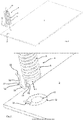
- wire 6 forms a fitting portion 12 that, by becoming elastically deformed, is configured for fitting into an aperture 14 of printed circuit board 2, so as to removably secure spring 4 to printed circuit board 2.
- assembling is effected in a simple, quick and removable manner. Furthermore, the assembly is compact and inexpensive, because no additional intermediate elements are required for fastening spring 4 to printed circuit board 2.
- wire 6 does not intersect the inner part of spring body 8.
- spring body 8 is formed by the coils of coil spring 4.
- aperture 14 is a slot.
- aperture 14, in particular the slot is a through opening, i.e. it goes through both faces of printed circuit board 2.
- Printed circuit board 2 may be of a per se known type, e.g. an electronic board, etc.
- the assembly comprises a support layer for supporting an electric/electronic circuit whereon spring 4 is mounted, in accordance with the present description.
- the support layer includes aperture or slot 14.
- One or more electric/electronic components constituting said electric/electronic circuit are mounted on the support layer.
- Coil spring 4 is preferably cylindrical, in particular it has a linear behaviour.
- Spring body 8 comprises, as is known, a plurality of coils. In this example, the coils are all substantially equal, and spring body 8 is cylindrical. Therefore, cavity 10 is also substantially cylindrical.
- spring 4, in particular spring body 8 may have different shapes, such as a truncated conical shape.
- a spring 4 having a non-linear behaviour may be used, e.g. a progressive spring, etc.
- Spring 4 is preferably made of electrically conductive material, e.g. metal or metal alloy.
- Spring 4 has two ends, one of which comprises fitting portion 12.
- Fitting portion 12 formed by wire 6 that forms spring body 8 as well, is in a distal position relative to spring body 8.
- fitting portion 12 is substantially parallel to the longitudinal axis x-x.
- Fitting portion 12 is configured for mounting spring 4 to printed circuit board 2 in a removable manner. Fitting portion 12 is configured for being inserted into and removed from aperture 14, in particular the slot, by applying a force that causes it to become elastically deformed, so that it can be inserted into and removed from aperture 14. Fitting portion 12 is therefore elastically deformable. It is thus possible to assemble and disassemble spring 4 and printed circuit board 2 by simply pushing and pulling spring 4 onto/from printed circuit board 2 and by applying the necessary force for deforming fitting portion 12. Therefore, no tools or other elements need to be used.
- fitting portion 12 has a hook-like shape.
- fitting portion 12 comprises a wider portion 16, located in a distal position (i.e. farther from spring body 8), and a narrower portion, located in a proximal position.
- the narrower portion comprises two first tracts 18, 20 of wire 6, preferably parallel to each other, and in particular parallel to the longitudinal axis x-x.
- Wider portion 16 is, therefore, a wire tract connecting the two first tracts 18, 20.
- wider portion 16 is curved.
- wider portion 16 comprises two shoulders 17, 19, located farther away compared to the two first tracts 18, 20. In the illustrated variant, shoulders 17, 19 define the width of wider portion 16, and the two first tracts 18, 20 define the width of the narrower portion.
- width of wider portion 16 slightly exceeds the length of the slot, so that wider portion 16 will become deformed to go through the slot upon exertion of a mechanical force, for the purpose of mounting or dismounting spring 4 onto/from printed circuit board 2.
- fitting portion 12 comprises a final tract 22 of wire 6, said final tract 22 being configured to limit the insertion of fitting portion 12 into aperture 14.
- final tract 22 protrudes from printed circuit board 2 on the side whereon spring 4 is located.
- final tract 22 may also act as a gripping portion for a user, who, by gripping final tract 22, can elastically deform fitting portion 12 to promote the extraction or insertion thereof from/into aperture 14.
- fitting portion 12 lies in a plane, in particular said plane being substantially parallel to the longitudinal axis x-x.
- the wire tracts designated by numerals 16, 18, 20, and preferably also the elements designated by numerals 17, 19, 22, lie in that plane.
- said plane is tangent to spring body 8.
- cavity 10 is an empty channel that runs through spring 4 parallel to the longitudinal axis x-x.
- fitting portion 12 is tangent to spring body 8.
- dashed lines L1, L2 schematically indicate the inner profile and, respectively, the outer profile of the projection of spring body 8 on printed circuit board 2.
- fitting portion 12 protrudes tangentially outwards from outer profile L2 of spring body 8.
- aperture 14, in particular the slot also protrudes outwards relative to the projection of spring body 8 on printed circuit board 2.
- printed circuit board 2 is electrically connected to spring 4 when the latter 4 is mounted to printed circuit board 2.
- fitting portion 12 and/or one or more coils are adapted for coming in contact with an electrically conductive portion, e.g. a metal portion, of printed circuit board 2.
- printed circuit board 2 includes an illuminating element 24 capable of emitting light and located within spring body 8, with reference to a plane perpendicular to the longitudinal axis x-x.
- Illuminating element 24 may be per se known, and preferably including a LED, or a bulb.
- the light beam emitted by illuminating element 24 can pass through cavity 10 without encountering any obstacle.
- Illuminating element 24 is therefore located near/at the first end of spring 4. This ensures very good visibility of the light emitted by said illuminating element 24 from the second end of spring 4.
- illuminating element 24 is substantially coaxial to the longitudinal axis x-x.
- the LED is soldered to printed circuit board 2.
- spring 4 is mounted to said printed circuit board 2.
- illuminating element 24 can be removably secured to printed circuit board 2.
- This assembly is advantageous in that it can be associated with a capacitive key, a switch or a button to provide visual feedback for the action executed thereon by the user, e.g. when it is touched or pressed.
- a capacitive key comprising:
- spring 4 which is made of electrically conductive material, acts as a first armature of a capacitor.
- the capacity of said capacitor will change, thus allowing a control unit to determine the presence of a part of the user's body on the external layer, so that predefined actions can be executed in response to that touch.
- the operation of a capacitive key will not be described any further, since it is per se known.
- the material of the external layer is an insulating material, e.g. plastic or glass.
- the external layer serves to avoid any contact between the part of the user's body, e.g. a finger, and spring 4.
- the external layer comprises an at least partially transparent portion, so that illuminating element 24, when it is emitting light, can be seen by the user through said at least partially transparent portion.
- Said capacitive key can be integrated into a control panel, which may possibly include other control elements, such as knobs, keys, displays, indicators, etc.
- the control panel may, for example, be mounted on a household appliance, such as a washing machine, an oven, a refrigerator, etc. It is therefore possible to provide visual feedback about an operating condition of the system with which the capacitive key is associated.
- the light emitted by illuminating element 24 may indicate the on or standby condition of the system (e.g. the household appliance), or it may indicate that a certain operation is being executed, a malfunctioning or faulty condition, or other conditions, according to the case.
Landscapes
- Engineering & Computer Science (AREA)
- Microelectronics & Electronic Packaging (AREA)
- Springs (AREA)
- Push-Button Switches (AREA)
Applications Claiming Priority (1)
| Application Number | Priority Date | Filing Date | Title |
|---|---|---|---|
| IT102017000011780A IT201700011780A1 (it) | 2017-02-03 | 2017-02-03 | Assieme comprendente un circuito stampato ed una molla elicoidale. |
Publications (2)
| Publication Number | Publication Date |
|---|---|
| EP3358746A1 true EP3358746A1 (fr) | 2018-08-08 |
| EP3358746B1 EP3358746B1 (fr) | 2022-08-31 |
Family
ID=59101564
Family Applications (1)
| Application Number | Title | Priority Date | Filing Date |
|---|---|---|---|
| EP18154593.0A Active EP3358746B1 (fr) | 2017-02-03 | 2018-02-01 | Ensemble comprenant une plaquette de circuits imprimés et un ressort a spirale |
Country Status (2)
| Country | Link |
|---|---|
| EP (1) | EP3358746B1 (fr) |
| IT (1) | IT201700011780A1 (fr) |
Cited By (2)
| Publication number | Priority date | Publication date | Assignee | Title |
|---|---|---|---|---|
| CN111417299A (zh) * | 2020-04-13 | 2020-07-14 | 温州职业技术学院 | 电路基板主体制作方法 |
| EP4001767A1 (fr) * | 2020-11-19 | 2022-05-25 | Electrolux Appliances Aktiebolag | Dispositif d'interaction d'utilisateur, appareil domestique et procédé de fabrication d'un dispositif d'interaction d'utilisateur |
Citations (3)
| Publication number | Priority date | Publication date | Assignee | Title |
|---|---|---|---|---|
| US4458293A (en) * | 1981-11-05 | 1984-07-03 | Cherry Electrical Products Corporation | Capacitive keyboard |
| CN105070560A (zh) * | 2015-08-18 | 2015-11-18 | 深圳市鼎隆盛塑胶模具有限公司 | 光感机械键盘 |
| US20160359246A1 (en) * | 2015-06-08 | 2016-12-08 | International Business Machines Corporation | Pin attach converter |
Family Cites Families (1)
| Publication number | Priority date | Publication date | Assignee | Title |
|---|---|---|---|---|
| KR100970197B1 (ko) * | 2008-07-11 | 2010-07-14 | 주식회사 비에스이 | 가변 지향성 마이크로폰 조립체 및 그 제조방법 |
-
2017
- 2017-02-03 IT IT102017000011780A patent/IT201700011780A1/it unknown
-
2018
- 2018-02-01 EP EP18154593.0A patent/EP3358746B1/fr active Active
Patent Citations (3)
| Publication number | Priority date | Publication date | Assignee | Title |
|---|---|---|---|---|
| US4458293A (en) * | 1981-11-05 | 1984-07-03 | Cherry Electrical Products Corporation | Capacitive keyboard |
| US20160359246A1 (en) * | 2015-06-08 | 2016-12-08 | International Business Machines Corporation | Pin attach converter |
| CN105070560A (zh) * | 2015-08-18 | 2015-11-18 | 深圳市鼎隆盛塑胶模具有限公司 | 光感机械键盘 |
Cited By (3)
| Publication number | Priority date | Publication date | Assignee | Title |
|---|---|---|---|---|
| CN111417299A (zh) * | 2020-04-13 | 2020-07-14 | 温州职业技术学院 | 电路基板主体制作方法 |
| CN111417299B (zh) * | 2020-04-13 | 2021-03-23 | 温州职业技术学院 | 电路基板主体制作方法 |
| EP4001767A1 (fr) * | 2020-11-19 | 2022-05-25 | Electrolux Appliances Aktiebolag | Dispositif d'interaction d'utilisateur, appareil domestique et procédé de fabrication d'un dispositif d'interaction d'utilisateur |
Also Published As
| Publication number | Publication date |
|---|---|
| EP3358746B1 (fr) | 2022-08-31 |
| IT201700011780A1 (it) | 2018-08-03 |
Similar Documents
| Publication | Publication Date | Title |
|---|---|---|
| EP2950613B1 (fr) | Ensemble de bobine d'induction et table de cuisson à induction comprenant un ensemble de bobine d'induction | |
| US6914206B2 (en) | Operation button fixing structure of electric device | |
| US3085139A (en) | Printed circuit mounting means for switch blades | |
| US20100141144A1 (en) | Lamp Comprising a Base and at Least Light-Emitting Semiconductor Component | |
| EP3358746A1 (fr) | Ensemble comprenant une plaquette de circuits imprimés et un ressort a spirale | |
| JP6631591B2 (ja) | プレスフィット端子及びその製造方法 | |
| US9691570B1 (en) | Modular tactile switch | |
| KR101989320B1 (ko) | 기판 접속용 커넥터 장치 | |
| JP2003134640A (ja) | 制御装置 | |
| CN109104178B (zh) | 电容式触摸组件以及控制面板 | |
| EP1763050A1 (fr) | Ensemble commutateur | |
| EP2672496A2 (fr) | Ajusteur de rapport de type disque | |
| JP2016015273A (ja) | プレスフィット端子 | |
| US7342191B2 (en) | Button assembly on computer panel | |
| JP2017017108A (ja) | 部品位置決め構造 | |
| JP2008108557A (ja) | タッチ検出機能付きスイッチ装置 | |
| JP2017126623A (ja) | 部品取付構造 | |
| KR100696104B1 (ko) | 시소형 스위치장치 | |
| CN205028818U (zh) | 按钮开关 | |
| CN211831562U (zh) | 一种电器盒体及电源控制装置 | |
| JP4772634B2 (ja) | 照光式ロッカスイッチ | |
| CN103180924A (zh) | 电开关 | |
| JP5907503B2 (ja) | 電子機器 | |
| JP4788483B2 (ja) | 電気機器の制御基板 | |
| KR200254384Y1 (ko) | 일체형 엘이디 디스플레이 장치 |
Legal Events
| Date | Code | Title | Description |
|---|---|---|---|
| PUAI | Public reference made under article 153(3) epc to a published international application that has entered the european phase |
Free format text: ORIGINAL CODE: 0009012 |
|
| STAA | Information on the status of an ep patent application or granted ep patent |
Free format text: STATUS: THE APPLICATION HAS BEEN PUBLISHED |
|
| AK | Designated contracting states |
Kind code of ref document: A1 Designated state(s): AL AT BE BG CH CY CZ DE DK EE ES FI FR GB GR HR HU IE IS IT LI LT LU LV MC MK MT NL NO PL PT RO RS SE SI SK SM TR |
|
| AX | Request for extension of the european patent |
Extension state: BA ME |
|
| STAA | Information on the status of an ep patent application or granted ep patent |
Free format text: STATUS: REQUEST FOR EXAMINATION WAS MADE |
|
| 17P | Request for examination filed |
Effective date: 20190118 |
|
| RBV | Designated contracting states (corrected) |
Designated state(s): AL AT BE BG CH CY CZ DE DK EE ES FI FR GB GR HR HU IE IS IT LI LT LU LV MC MK MT NL NO PL PT RO RS SE SI SK SM TR |
|
| STAA | Information on the status of an ep patent application or granted ep patent |
Free format text: STATUS: EXAMINATION IS IN PROGRESS |
|
| 17Q | First examination report despatched |
Effective date: 20200625 |
|
| GRAP | Despatch of communication of intention to grant a patent |
Free format text: ORIGINAL CODE: EPIDOSNIGR1 |
|
| STAA | Information on the status of an ep patent application or granted ep patent |
Free format text: STATUS: GRANT OF PATENT IS INTENDED |
|
| INTG | Intention to grant announced |
Effective date: 20220425 |
|
| GRAS | Grant fee paid |
Free format text: ORIGINAL CODE: EPIDOSNIGR3 |
|
| GRAA | (expected) grant |
Free format text: ORIGINAL CODE: 0009210 |
|
| STAA | Information on the status of an ep patent application or granted ep patent |
Free format text: STATUS: THE PATENT HAS BEEN GRANTED |
|
| AK | Designated contracting states |
Kind code of ref document: B1 Designated state(s): AL AT BE BG CH CY CZ DE DK EE ES FI FR GB GR HR HU IE IS IT LI LT LU LV MC MK MT NL NO PL PT RO RS SE SI SK SM TR |
|
| REG | Reference to a national code |
Ref country code: CH Ref legal event code: EP Ref country code: GB Ref legal event code: FG4D |
|
| REG | Reference to a national code |
Ref country code: AT Ref legal event code: REF Ref document number: 1516053 Country of ref document: AT Kind code of ref document: T Effective date: 20220915 |
|
| REG | Reference to a national code |
Ref country code: DE Ref legal event code: R096 Ref document number: 602018039891 Country of ref document: DE |
|
| REG | Reference to a national code |
Ref country code: IE Ref legal event code: FG4D |
|
| REG | Reference to a national code |
Ref country code: LT Ref legal event code: MG9D |
|
| REG | Reference to a national code |
Ref country code: NL Ref legal event code: MP Effective date: 20220831 |
|
| PG25 | Lapsed in a contracting state [announced via postgrant information from national office to epo] |
Ref country code: SE Free format text: LAPSE BECAUSE OF FAILURE TO SUBMIT A TRANSLATION OF THE DESCRIPTION OR TO PAY THE FEE WITHIN THE PRESCRIBED TIME-LIMIT Effective date: 20220831 Ref country code: RS Free format text: LAPSE BECAUSE OF FAILURE TO SUBMIT A TRANSLATION OF THE DESCRIPTION OR TO PAY THE FEE WITHIN THE PRESCRIBED TIME-LIMIT Effective date: 20220831 Ref country code: NO Free format text: LAPSE BECAUSE OF FAILURE TO SUBMIT A TRANSLATION OF THE DESCRIPTION OR TO PAY THE FEE WITHIN THE PRESCRIBED TIME-LIMIT Effective date: 20221130 Ref country code: LV Free format text: LAPSE BECAUSE OF FAILURE TO SUBMIT A TRANSLATION OF THE DESCRIPTION OR TO PAY THE FEE WITHIN THE PRESCRIBED TIME-LIMIT Effective date: 20220831 Ref country code: LT Free format text: LAPSE BECAUSE OF FAILURE TO SUBMIT A TRANSLATION OF THE DESCRIPTION OR TO PAY THE FEE WITHIN THE PRESCRIBED TIME-LIMIT Effective date: 20220831 Ref country code: FI Free format text: LAPSE BECAUSE OF FAILURE TO SUBMIT A TRANSLATION OF THE DESCRIPTION OR TO PAY THE FEE WITHIN THE PRESCRIBED TIME-LIMIT Effective date: 20220831 |
|
| REG | Reference to a national code |
Ref country code: AT Ref legal event code: MK05 Ref document number: 1516053 Country of ref document: AT Kind code of ref document: T Effective date: 20220831 |
|
| PG25 | Lapsed in a contracting state [announced via postgrant information from national office to epo] |
Ref country code: PL Free format text: LAPSE BECAUSE OF FAILURE TO SUBMIT A TRANSLATION OF THE DESCRIPTION OR TO PAY THE FEE WITHIN THE PRESCRIBED TIME-LIMIT Effective date: 20220831 Ref country code: IS Free format text: LAPSE BECAUSE OF FAILURE TO SUBMIT A TRANSLATION OF THE DESCRIPTION OR TO PAY THE FEE WITHIN THE PRESCRIBED TIME-LIMIT Effective date: 20221231 Ref country code: HR Free format text: LAPSE BECAUSE OF FAILURE TO SUBMIT A TRANSLATION OF THE DESCRIPTION OR TO PAY THE FEE WITHIN THE PRESCRIBED TIME-LIMIT Effective date: 20220831 Ref country code: GR Free format text: LAPSE BECAUSE OF FAILURE TO SUBMIT A TRANSLATION OF THE DESCRIPTION OR TO PAY THE FEE WITHIN THE PRESCRIBED TIME-LIMIT Effective date: 20221201 |
|
| PG25 | Lapsed in a contracting state [announced via postgrant information from national office to epo] |
Ref country code: SM Free format text: LAPSE BECAUSE OF FAILURE TO SUBMIT A TRANSLATION OF THE DESCRIPTION OR TO PAY THE FEE WITHIN THE PRESCRIBED TIME-LIMIT Effective date: 20220831 Ref country code: RO Free format text: LAPSE BECAUSE OF FAILURE TO SUBMIT A TRANSLATION OF THE DESCRIPTION OR TO PAY THE FEE WITHIN THE PRESCRIBED TIME-LIMIT Effective date: 20220831 Ref country code: PT Free format text: LAPSE BECAUSE OF FAILURE TO SUBMIT A TRANSLATION OF THE DESCRIPTION OR TO PAY THE FEE WITHIN THE PRESCRIBED TIME-LIMIT Effective date: 20230102 Ref country code: ES Free format text: LAPSE BECAUSE OF FAILURE TO SUBMIT A TRANSLATION OF THE DESCRIPTION OR TO PAY THE FEE WITHIN THE PRESCRIBED TIME-LIMIT Effective date: 20220831 Ref country code: DK Free format text: LAPSE BECAUSE OF FAILURE TO SUBMIT A TRANSLATION OF THE DESCRIPTION OR TO PAY THE FEE WITHIN THE PRESCRIBED TIME-LIMIT Effective date: 20220831 Ref country code: CZ Free format text: LAPSE BECAUSE OF FAILURE TO SUBMIT A TRANSLATION OF THE DESCRIPTION OR TO PAY THE FEE WITHIN THE PRESCRIBED TIME-LIMIT Effective date: 20220831 Ref country code: AT Free format text: LAPSE BECAUSE OF FAILURE TO SUBMIT A TRANSLATION OF THE DESCRIPTION OR TO PAY THE FEE WITHIN THE PRESCRIBED TIME-LIMIT Effective date: 20220831 |
|
| PG25 | Lapsed in a contracting state [announced via postgrant information from national office to epo] |
Ref country code: SK Free format text: LAPSE BECAUSE OF FAILURE TO SUBMIT A TRANSLATION OF THE DESCRIPTION OR TO PAY THE FEE WITHIN THE PRESCRIBED TIME-LIMIT Effective date: 20220831 Ref country code: EE Free format text: LAPSE BECAUSE OF FAILURE TO SUBMIT A TRANSLATION OF THE DESCRIPTION OR TO PAY THE FEE WITHIN THE PRESCRIBED TIME-LIMIT Effective date: 20220831 |
|
| REG | Reference to a national code |
Ref country code: DE Ref legal event code: R097 Ref document number: 602018039891 Country of ref document: DE |
|
| P01 | Opt-out of the competence of the unified patent court (upc) registered |
Effective date: 20230519 |
|
| PG25 | Lapsed in a contracting state [announced via postgrant information from national office to epo] |
Ref country code: NL Free format text: LAPSE BECAUSE OF FAILURE TO SUBMIT A TRANSLATION OF THE DESCRIPTION OR TO PAY THE FEE WITHIN THE PRESCRIBED TIME-LIMIT Effective date: 20220831 Ref country code: AL Free format text: LAPSE BECAUSE OF FAILURE TO SUBMIT A TRANSLATION OF THE DESCRIPTION OR TO PAY THE FEE WITHIN THE PRESCRIBED TIME-LIMIT Effective date: 20220831 |
|
| PLBE | No opposition filed within time limit |
Free format text: ORIGINAL CODE: 0009261 |
|
| STAA | Information on the status of an ep patent application or granted ep patent |
Free format text: STATUS: NO OPPOSITION FILED WITHIN TIME LIMIT |
|
| 26N | No opposition filed |
Effective date: 20230601 |
|
| PG25 | Lapsed in a contracting state [announced via postgrant information from national office to epo] |
Ref country code: SI Free format text: LAPSE BECAUSE OF FAILURE TO SUBMIT A TRANSLATION OF THE DESCRIPTION OR TO PAY THE FEE WITHIN THE PRESCRIBED TIME-LIMIT Effective date: 20220831 |
|
| PG25 | Lapsed in a contracting state [announced via postgrant information from national office to epo] |
Ref country code: MC Free format text: LAPSE BECAUSE OF FAILURE TO SUBMIT A TRANSLATION OF THE DESCRIPTION OR TO PAY THE FEE WITHIN THE PRESCRIBED TIME-LIMIT Effective date: 20220831 |
|
| REG | Reference to a national code |
Ref country code: CH Ref legal event code: PL |
|
| REG | Reference to a national code |
Ref country code: BE Ref legal event code: MM Effective date: 20230228 |
|
| PG25 | Lapsed in a contracting state [announced via postgrant information from national office to epo] |
Ref country code: LU Free format text: LAPSE BECAUSE OF NON-PAYMENT OF DUE FEES Effective date: 20230201 Ref country code: LI Free format text: LAPSE BECAUSE OF NON-PAYMENT OF DUE FEES Effective date: 20230228 Ref country code: CH Free format text: LAPSE BECAUSE OF NON-PAYMENT OF DUE FEES Effective date: 20230228 |
|
| REG | Reference to a national code |
Ref country code: IE Ref legal event code: MM4A |
|
| PG25 | Lapsed in a contracting state [announced via postgrant information from national office to epo] |
Ref country code: IE Free format text: LAPSE BECAUSE OF NON-PAYMENT OF DUE FEES Effective date: 20230201 |
|
| PG25 | Lapsed in a contracting state [announced via postgrant information from national office to epo] |
Ref country code: BE Free format text: LAPSE BECAUSE OF NON-PAYMENT OF DUE FEES Effective date: 20230228 |
|
| PGFP | Annual fee paid to national office [announced via postgrant information from national office to epo] |
Ref country code: GB Payment date: 20240222 Year of fee payment: 7 |
|
| PG25 | Lapsed in a contracting state [announced via postgrant information from national office to epo] |
Ref country code: IT Free format text: LAPSE BECAUSE OF FAILURE TO SUBMIT A TRANSLATION OF THE DESCRIPTION OR TO PAY THE FEE WITHIN THE PRESCRIBED TIME-LIMIT Effective date: 20220831 |
|
| REG | Reference to a national code |
Ref country code: DE Ref legal event code: R081 Ref document number: 602018039891 Country of ref document: DE Owner name: BITRON ELECTRONICS S.P.A., IT Free format text: FORMER OWNER: BITRON S.P.A., TORINO, IT |
|
| PG25 | Lapsed in a contracting state [announced via postgrant information from national office to epo] |
Ref country code: BG Free format text: LAPSE BECAUSE OF FAILURE TO SUBMIT A TRANSLATION OF THE DESCRIPTION OR TO PAY THE FEE WITHIN THE PRESCRIBED TIME-LIMIT Effective date: 20220831 |
|
| PG25 | Lapsed in a contracting state [announced via postgrant information from national office to epo] |
Ref country code: BG Free format text: LAPSE BECAUSE OF FAILURE TO SUBMIT A TRANSLATION OF THE DESCRIPTION OR TO PAY THE FEE WITHIN THE PRESCRIBED TIME-LIMIT Effective date: 20220831 |
|
| PG25 | Lapsed in a contracting state [announced via postgrant information from national office to epo] |
Ref country code: CY Free format text: LAPSE BECAUSE OF FAILURE TO SUBMIT A TRANSLATION OF THE DESCRIPTION OR TO PAY THE FEE WITHIN THE PRESCRIBED TIME-LIMIT; INVALID AB INITIO Effective date: 20180201 |
|
| PG25 | Lapsed in a contracting state [announced via postgrant information from national office to epo] |
Ref country code: HU Free format text: LAPSE BECAUSE OF FAILURE TO SUBMIT A TRANSLATION OF THE DESCRIPTION OR TO PAY THE FEE WITHIN THE PRESCRIBED TIME-LIMIT; INVALID AB INITIO Effective date: 20180201 |
|
| GBPC | Gb: european patent ceased through non-payment of renewal fee |
Effective date: 20250201 |
|
| PG25 | Lapsed in a contracting state [announced via postgrant information from national office to epo] |
Ref country code: TR Free format text: LAPSE BECAUSE OF FAILURE TO SUBMIT A TRANSLATION OF THE DESCRIPTION OR TO PAY THE FEE WITHIN THE PRESCRIBED TIME-LIMIT Effective date: 20220831 |
|
| PG25 | Lapsed in a contracting state [announced via postgrant information from national office to epo] |
Ref country code: GB Free format text: LAPSE BECAUSE OF NON-PAYMENT OF DUE FEES Effective date: 20250201 |
|
| PGFP | Annual fee paid to national office [announced via postgrant information from national office to epo] |
Ref country code: DE Payment date: 20260217 Year of fee payment: 9 |
|
| PGFP | Annual fee paid to national office [announced via postgrant information from national office to epo] |
Ref country code: FR Payment date: 20260213 Year of fee payment: 9 |