EP3360249B1 - Amplifikationsvorrichtung mit begrenzung - Google Patents
Amplifikationsvorrichtung mit begrenzung Download PDFInfo
- Publication number
- EP3360249B1 EP3360249B1 EP15781317.1A EP15781317A EP3360249B1 EP 3360249 B1 EP3360249 B1 EP 3360249B1 EP 15781317 A EP15781317 A EP 15781317A EP 3360249 B1 EP3360249 B1 EP 3360249B1
- Authority
- EP
- European Patent Office
- Prior art keywords
- signal
- output
- input
- stage
- coupled
- Prior art date
- Legal status (The legal status is an assumption and is not a legal conclusion. Google has not performed a legal analysis and makes no representation as to the accuracy of the status listed.)
- Active
Links
Images



Classifications
-
- H—ELECTRICITY
- H03—ELECTRONIC CIRCUITRY
- H03F—AMPLIFIERS
- H03F1/00—Details of amplifiers with only discharge tubes, only semiconductor devices or only unspecified devices as amplifying elements
- H03F1/52—Circuit arrangements for protecting such amplifiers
- H03F1/523—Circuit arrangements for protecting such amplifiers for amplifiers using field-effect devices
-
- H—ELECTRICITY
- H03—ELECTRONIC CIRCUITRY
- H03F—AMPLIFIERS
- H03F1/00—Details of amplifiers with only discharge tubes, only semiconductor devices or only unspecified devices as amplifying elements
- H03F1/52—Circuit arrangements for protecting such amplifiers
-
- H—ELECTRICITY
- H03—ELECTRONIC CIRCUITRY
- H03F—AMPLIFIERS
- H03F3/00—Amplifiers with only discharge tubes or only semiconductor devices as amplifying elements
- H03F3/189—High-frequency amplifiers, e.g. radio frequency amplifiers
-
- H—ELECTRICITY
- H03—ELECTRONIC CIRCUITRY
- H03F—AMPLIFIERS
- H03F3/00—Amplifiers with only discharge tubes or only semiconductor devices as amplifying elements
- H03F3/189—High-frequency amplifiers, e.g. radio frequency amplifiers
- H03F3/19—High-frequency amplifiers, e.g. radio frequency amplifiers with semiconductor devices only
- H03F3/193—High-frequency amplifiers, e.g. radio frequency amplifiers with semiconductor devices only with field-effect devices
-
- H—ELECTRICITY
- H03—ELECTRONIC CIRCUITRY
- H03F—AMPLIFIERS
- H03F3/00—Amplifiers with only discharge tubes or only semiconductor devices as amplifying elements
- H03F3/45—Differential amplifiers
-
- H—ELECTRICITY
- H03—ELECTRONIC CIRCUITRY
- H03F—AMPLIFIERS
- H03F3/00—Amplifiers with only discharge tubes or only semiconductor devices as amplifying elements
- H03F3/45—Differential amplifiers
- H03F3/45071—Differential amplifiers with semiconductor devices only
- H03F3/45076—Differential amplifiers with semiconductor devices only characterised by the way of implementation of the active amplifying circuit in the differential amplifier
- H03F3/45179—Differential amplifiers with semiconductor devices only characterised by the way of implementation of the active amplifying circuit in the differential amplifier using MOSFET transistors as the active amplifying circuit
-
- H—ELECTRICITY
- H03—ELECTRONIC CIRCUITRY
- H03G—CONTROL OF AMPLIFICATION
- H03G3/00—Gain control in amplifiers or frequency changers
- H03G3/20—Automatic control
- H03G3/30—Automatic control in amplifiers having semiconductor devices
- H03G3/3036—Automatic control in amplifiers having semiconductor devices in high-frequency amplifiers or in frequency-changers
-
- H—ELECTRICITY
- H04—ELECTRIC COMMUNICATION TECHNIQUE
- H04B—TRANSMISSION
- H04B1/00—Details of transmission systems, not covered by a single one of groups H04B3/00 - H04B13/00; Details of transmission systems not characterised by the medium used for transmission
- H04B1/06—Receivers
- H04B1/16—Circuits
-
- H—ELECTRICITY
- H03—ELECTRONIC CIRCUITRY
- H03F—AMPLIFIERS
- H03F2200/00—Indexing scheme relating to amplifiers
- H03F2200/294—Indexing scheme relating to amplifiers the amplifier being a low noise amplifier [LNA]
-
- H—ELECTRICITY
- H03—ELECTRONIC CIRCUITRY
- H03F—AMPLIFIERS
- H03F2200/00—Indexing scheme relating to amplifiers
- H03F2200/372—Noise reduction and elimination in amplifier
-
- H—ELECTRICITY
- H03—ELECTRONIC CIRCUITRY
- H03F—AMPLIFIERS
- H03F2203/00—Indexing scheme relating to amplifiers with only discharge tubes or only semiconductor devices as amplifying elements covered by H03F3/00
- H03F2203/45—Indexing scheme relating to differential amplifiers
- H03F2203/45116—Feedback coupled to the input of the differential amplifier
-
- H—ELECTRICITY
- H03—ELECTRONIC CIRCUITRY
- H03F—AMPLIFIERS
- H03F2203/00—Indexing scheme relating to amplifiers with only discharge tubes or only semiconductor devices as amplifying elements covered by H03F3/00
- H03F2203/45—Indexing scheme relating to differential amplifiers
- H03F2203/45526—Indexing scheme relating to differential amplifiers the FBC comprising a resistor-capacitor combination and being coupled between the LC and the IC
Definitions
- the present disclosure relates to an amplification device, a receiving apparatus comprising the amplification device, and a radio communication apparatus comprising the receiving apparatus, and has application in particular, but not exclusively, to radio frequency integrated circuits.
- Radio frequency integrated circuits include increasing amounts of digital processing which, because radio frequency (RF) spectrum is a scarce resource, are required to operate in higher and higher frequency bands. For example, recently, frequency bands in the range 3 to 6GHz are being deployed for the third generation partnership project (3GPP). In addition, target power consumption is continually being reduced. In response to these factors, RFICs are being implemented in deep complementary metal oxide semiconductor (CMOS) nodes using, for example, 28nm technology.
- CMOS complementary metal oxide semiconductor
- LNA low noise amplifier
- a User Equipment (UE) supporting multiple simultaneous 3GPP systems and/or WiFi might generate significant interference to its own receivers due to crosstalk between antennas.
- UE User Equipment
- a particularly challenging scenario is a small cell base station deployed indoors.
- some UEs may be connected to an indoor system while other UEs are connected to an outdoor system, for example using an operator not available indoors, with all UEs potentially operating in the same frequency band.
- a UE connected to the outdoor system will transmit at a much higher output power than those connected to the indoor system, in order to be able to reach the outdoor base stations. This could cause high levels of interference in the LNAs of the indoor base station, sufficient to damage them.
- a UE connected to the outdoor system may act as a blocker to the indoor system and degrade all communication in that frequency band.
- Another challenging scenario relates to beam forming radios, where preferably no filters are used before the LNA as a high number of antennas may be employed, for example in the order of a hundred. In this case high power out-of-band signals may enter the LNA and damage it.
- an amplification device comprising:
- limiting may be applied at the first signal output, using a threshold dependent on the difference between the threshold control signal and the feedback signal.
- the amplification device can provide protection against damage to the amplifier circuit by providing limiting at the first signal output, whilst enabling reduced degradation of a wanted signal by providing the limiting only when needed for protection.
- the threshold control signal may be chosen to set the threshold of limiting to suit prevailing conditions.
- the use of feedback to establish the threshold signal enables the threshold signal to be set precisely and to be constant.
- the use of feedback to establish the threshold signal also enables the onset of limiting, when the input signal level increases, to be fast without significant hysteresis and without generating significant transient signals.
- the use of feedback enables the resumption of linear operation to occur without significant hysteresis and without generating significant transient signals.
- the threshold control signal may be provided from a source external to the amplification device.
- the limiter may comprise a threshold controller arranged to generate the threshold control signal dependent on a property of the amplifier circuit. This feature enables improved performance by enabling the threshold signal to be adapted to prevailing conditions or to the characteristics of the amplifier circuit, in particular to maximise the threshold of limiting whilst minimising the likelihood of damage to the amplifier circuit.
- the property of the amplifier circuit may be temperature of the amplifier. This enables the threshold signal to be adapted according to temperature changes circuit.
- the property of the amplifier circuit may be an integrated circuit process corner. This enables the threshold signal to be adapted according to the electrical characteristics of circuit components of the amplifier circuit.
- the differential amplifier may comprise a detector stage arranged to generate an averaged signal indicative of an average of a difference between the threshold control signal and the feedback signal, the amplification device may further comprises a gain control stage arranged to generate a gain control signal dependent on the averaged signal, and the amplifier circuit may be arranged to have a gain dependent on the gain control signal.
- PAPR peak-to-average power ratio
- the gain control stage may be arranged to control the gain control signal such that the gain of the amplifier circuit is increased in response to the averaged signal being indicative of the input signal having a level below a lower signal level threshold, is decreased in response to the averaged signal being indicative of the input signal having a level above an upper signal level threshold, and is unchanged in response to the averaged signal being indicative of the input signal having a level between the lower signal level threshold and the upper signal level threshold.
- the detector stage may be arranged to employ an adjustable time constant for generating the averaged signal, and the limiter may further comprise a time constant controller coupled to the detector stage and arranged to adjust the adjustable time constant dependent on a property of the input signal to be amplified.
- the property of the input signal may be type of modulation.
- the property of the input signal may be signal-to-interference ratio.
- the differential amplifier may comprise a differential input stage and an output stage, wherein a first input of the differential input stage is coupled to the first differential amplifier input and a second input of the differential input stage is coupled to the second differential amplifier input, wherein an input of the output stage is coupled to an output of the differential input stage and an output of the output stage is coupled to the difference output of the differential amplifier, and the detector stage may be coupled to the output of the differential input stage for determining the averaged signal.
- the detector stage may be arranged to replicate a current flowing in the output stage by generating a current proportional to a current flowing in the output stage, and may be arranged to generate the averaged signal from the replica. This feature enables the gain control of the amplifier circuit to accurately reflect changes in the threshold signal, and thereby accurately reflect the level of the input signal.
- the amplifier circuit may comprise a second signal output for a second output signal, the first and second output signals together forming a differential signal, and the limiter may comprise a second diode having a second anode coupled to the second signal output and a second cathode coupled to the differential amplifier output. This feature enables the amplification device to be used for delivering a differential signal.
- the feedback stage may comprise a capacitive element coupled between the differential amplifier output and a first voltage supply rail. This feature enables transients in the threshold signal to be reduced.
- the feedback stage may comprise a first resistive element coupled between the differential amplifier output and the second differential amplifier input, and a second resistive element coupled between the second differential amplifier input and a second power supply rail. This feature enables the differential amplifier to operate with low signal levels, and therefore have low power consumption.
- the amplifier circuit may be a low noise amplifier (LNA). Such an amplifier may therefore be deployed in the front end of a radio receiver.
- LNA low noise amplifier
- a receiving apparatus comprising the amplification device according to the first aspect.
- a radio communication apparatus comprising the receiving apparatus according to the second aspect.
- the radio communication apparatus may be a base station.
- the radio communication apparatus may be a mobile phone.
- amplification device comprising:
- Amplifying the input signal may further comprise providing a second output signal at a second output of the amplifier circuit, wherein the first and second output signals together form a differential signal, and the method may further comprise limiting the second output signal by means of a second diode having a second anode coupled to the second output of the amplifier circuit and a second cathode couple to the output of the differential amplifier.
- an amplification device 100 arranged for amplifying a single-ended signal comprises an amplifier circuit (AMP) 110, which may be an LNA, and a limiter 120.
- the amplifier circuit 110 has a signal input 111 for an input signal V i to be amplified and a first signal output 112 for a first output signal V O+ .
- the signal input 111 is arranged for receiving the input signal V i in a single-ended format, although in other embodiments the signal input 11 may be arranged for receiving the input signal V i in a differential format.
- the signal input 111 of the amplifier circuit 110 is also a signal input of the amplification device 100, and the first signal output 112 is also a signal output of the amplification device 100.
- the limiter 120 has a differential amplifier 125.
- the differential amplifier 125 comprises a first differential amplifier input 129 for a threshold control signal V C a second differential amplifier input 113 for a feedback signal V FB , and a differential amplifier output 124 for a threshold signal V TH indicative of a difference between the threshold control signal V C and the feedback signal V FB .
- the first differential amplifier input 129 is a non-inverting input and the second differential amplifier input 113 is an inverting input.
- the threshold control signal V C and the feedback signal V FB are voltages.
- a first diode 121 has a first anode 122 coupled to the first signal output 112 of the amplifier circuit 110 and a first cathode 123 coupled to the differential amplifier output 124.
- Diodes are commonly available in integrated circuits for electrostatic discharge (ESD) protection, and the first diode 121 may be such a diode, scaled down in size, if desired, to reduce parasitic capacitance and therefore impact on tuning range.
- a feedback stage 128 is coupled between the differential amplifier output 124 and the second differential amplifier input 113, and is arranged to generate the feedback signal V FB dependent on the threshold signal V TH at the differential amplifier output 124.
- the first diode 121 In operation, for relatively low voltage levels of the input signal V i , the first output signal V O+ has a low level, the first diode 121 is reversed biased and the input signal V i is amplified without any limiting occurring.
- the threshold signal V TH has a constant quiescent level determined by the threshold control signal V C .
- the feedback signal V FB increases, and by operation of the differential amplifier 125, the threshold signal V TH is restored to its quiescent level, such that the amplitude of the first output signal V O+ is limited to the quiescent level of the threshold signal V TH plus the forward bias voltage of the first diode 121.
- the differential amplifier 125 may have to sink a high current, for example several milliamps.
- the differential amplifier 125 may have an output stage biased in class AB, which can enable the current in the differential amplifier 125 to be low, for example in the range 100 ⁇ A to 200 ⁇ A.
- the limiter 120 also comprises a threshold controller (ThC) 134 that is arranged to generate the threshold control signal V C . Therefore, in this embodiment, the threshold control signal V C is provided by a threshold controller 134 that is an integral element of the amplification device 100, whereas in other embodiments the threshold controller 134 may be omitted, in which case the threshold control signal V C may be provided by a device external to the amplification device 100.
- ThC threshold controller
- the threshold controller 134 may be arranged to generate the threshold control signal V C dependent on a property of the amplifier circuit 110.
- a property of the amplifier circuit 110 may be temperature of the amplifier circuit 110, in which case the threshold controller 134 may be arranged to measure temperature of the amplifier circuit 110 and to determine the threshold control signal V C dependent on the measured temperature.
- such a property of the amplifier circuit 110 may be a process corner of an integrated circuit in which the amplifier circuit 110, or the amplification device 100, is implemented, in which case the threshold controller 134 may be arranged to measure a parameter of the integrated circuit that is indicative of the process corner, such as a free-running ring oscillator clock frequency, as faster integrated circuits are more susceptible to over voltage, and to determine the threshold control signal V C dependent on the measured parameters.
- the property of the amplifier circuit 110 may be a property of one or more transistors within the amplifier circuit 110, in which case the property may be, for example, temperature of the transistor(s), or the threshold controller 134 may be arranged to measure a parameter of the transistor(s) that is indicative of the process corner.
- an amplification device 200 comprises an amplifier circuit 210 and a limiter 220.
- the amplifier circuit 210 has a signal input 211 for an input signal V i to be amplified.
- the signal input 211 comprises a first signal input 208 for a first input signal component, or first input signal part, V i+ of the input signal V i , and a second signal input 209 for a second input signal component, or second input signal part, V i- of the input signal V i , the first and second input signal components V i+ , V l- being an inversion of each other.
- the first and second input signal components V i+ , V i- form a differential signal.
- the signal input 211 may be arranged for a single ended input signal V i .
- the amplifier circuit 210 also comprises a first signal output 212 for a first output signal V O+ , and a second signal output 213 for a second output signal V O- .
- the first and second output signals V O+ , V O- form a differential signal, with the first and second output signals V O+ , V O- being an inversion of each other, at least when no limiting is taking place.
- the signal input 211 of the amplifier circuit 210 is also a signal input of the amplification device 200, and the first and second signal outputs 212, 213 are also first and second signal outputs of the amplification device 200.
- the limiter 220 has a differential amplifier 225.
- the differential amplifier 225 comprises a first differential amplifier input 229 for a threshold control signal V C a second differential amplifier input 230 for a feedback signal V FB , and a differential amplifier output 224 for a threshold signal V TH indicative of a difference between the threshold control signal V C and the feedback signal V FB .
- the first differential amplifier input 229 is a non-inverting input and the second differential amplifier input 230 is an inverting input.
- the threshold control signal V C and the feedback signal V FB are voltages.
- a first diode 221 has a first anode 222 coupled to the first signal output 212 of the amplifier circuit 210 and a first cathode 223 coupled to the differential amplifier output 224.
- a second diode 235 has a second anode 236 coupled to the second signal output 213 of the amplifier circuit 210 and a second cathode 237 coupled to the differential amplifier output 224.
- a feedback stage 228 is coupled between the differential amplifier output 224 and the second differential amplifier input 230, and is arranged to generate the feedback signal V FB dependent on the threshold signal V TH at the differential amplifier output 224.
- the feedback stage 228 comprises a capacitive element 226 coupled between the differential amplifier output 224 and a first voltage supply rail 227, which in this embodiment is at ground potential.
- the feedback stage 228 comprises a first resistive element 231 coupled between the differential amplifier output 224 and the second differential amplifier input 230, and a second resistive element 232 coupled between the second differential amplifier input 230 and a second power supply rail 233, which in this embodiment is at ground potential.
- the first output signal V O+ has a low level
- the first diode 221 is reversed biased and the input signal V i is amplified without any limiting occurring.
- the threshold signal V TH has a constant quiescent level determined by the threshold control signal V C .
- the feedback signal V FB increases, and by operation of the differential amplifier 225, the threshold signal V TH is restored to its quiescent level, such that the level of the first output signal V O+ is limited to the quiescent level of the threshold signal V TH plus the forward bias voltage of the first diode 221.
- the second diode 235 starts to conduct, which results in the level of the threshold signal V TH at the differential amplifier output 224 rising.
- the feedback signal V FB increases, and by operation of the differential amplifier 225, the threshold signal V TH is restored to its quiescent level, such that the level of the second output signal V O- is limited to the quiescent level of the threshold signal V TH plus the forward bias voltage of the second diode 235. Because the first and second output signals V O+ , V O- are both limited using the same threshold voltage V TH , limiting of the first and second output signals V O+ , V O- will not occur simultaneously, and the limiting will not be applied symmetrically to both the first and second output signals V O+ , V O- .
- Limiting is applied to the first or second output signals V O+ , V O- only when necessary to prevent one of these signals exceeding a chosen level, thereby enabling distortion of the first and second output signals V O+ , V O- to be minimised.
- the threshold signal V TH is used for limiting both the first and second output signals V O+ , V O- , thereby applying the same threshold of limiting to both the first and second output signals V O+ , V O- .
- the differential amplifier 225 when the input signal V i is relatively small, the differential amplifier 225 may have to sink a high current, for example several milliamps. In order to avoid a high current for long periods of time when the input signal V i is large for a long period of time, the differential amplifier 225 may have an output stage biased in class AB.
- the limiter 220 also comprises a threshold controller (ThC) 234 that is arranged to generate the threshold control signal V C .
- ThC threshold controller
- the threshold control signal V C is provided by a threshold controller 234 that is an integral element of the amplification device 200, whereas in other embodiments the threshold controller 234 may be omitted, in which case the threshold control signal V C may be provided by a device external to the amplification device 200.
- the threshold controller 234 may be arranged to generate the threshold control signal V C dependent on a property of the amplifier circuit 210.
- a property of the amplifier circuit 210 may be temperature of the amplifier circuit 210, in which case the threshold controller 234 may be arranged to measure temperature of the amplifier circuit 210 and to determine the threshold control signal V C dependent on the measured temperature.
- a property of the amplifier circuit 210 may be a process corner of an integrated circuit in which the amplifier circuit 210, or the amplification device 200, is implemented, in which case the threshold controller 234 may be arranged to measure parameters of the integrated circuit, such as currents and voltages, that are indicative of the process corner and to determine the threshold control signal V C dependent on the measured parameters.
- the property of the amplifier circuit 210 may be a property of one or more transistors within the amplifier circuit 210, such as the first, second, third and fourth transistors T 1 , T 2 , T 3 , T 4 of the amplifier circuit 210 described below with reference to Figure 5 , in which case the property may be, for example, temperature of the transistor(s), or the threshold controller 234 may be arranged to measure a parameter of the transistor(s) that is indicative of the process corner.
- the feedback stage 228 may have a different architecture than described above.
- the capacitive element 226 and/or the second resistive element 232 may be omitted, either or both being replaced by an open circuit.
- the first resistive element 231 may be replaced by a short circuit, in which case the feedback stage 228 provides a direct coupling between the differential amplifier output 224 and the second differential amplifier input 230.
- the capacitive element 226 and/or the second resistive element 232 may remain present, or may be omitted, either or both being replaced by an open circuit.
- the feedback stage 128 of the amplification device 100 described with reference to Figure 1 may have any of the architectures of the feedback stage 228 of the amplification device 200 described above.
- an amplification device 300 comprises all of the elements of the amplification device 200 described with reference to Figure 2 , and these elements will therefore not be described again below. Those elements of the amplification device 300 that are not also present in the amplification device 200 are described below.
- the amplification device 300 additionally comprises a gain controller (GC) 345, and the amplifier circuit 210 has a gain control input 354 by which the gain of the amplifier circuit 210 may be controlled.
- Figure 3 also illustrates a typical architecture of the differential amplifier 225, which may also apply to the differential amplifier 125 of Figure 1 , although other architectures may be used instead.
- the differential amplifier 225 comprises a differential input stage (I/P) 350, a detector stage (DET) 340, and an output stage (O/P) 360.
- a first input 351 of the differential input stage 350 is coupled to the first differential amplifier input 229 for receiving the threshold control signal V C and a second input 352 of the differential input stage 350 is coupled to the second differential amplifier input 230 for receiving the feedback signal V FB .
- the first input 351 of the differential input stage 350 is a non-inverting input and the second differential amplifier input 352 is an inverting input.
- An output 353 of the differential input stage 350 delivers a difference signal V ⁇ that is indicative of the difference between the threshold control signal V C and the feedback signal V FB .
- An input 361 of the output stage 360 is coupled to the output 353 of the differential input stage 350, and an output 362 of the output stage 360 is coupled to the difference output 224 of the differential amplifier 225 for delivering the threshold signal V TH .
- a first input 341 of the detector stage 340 is coupled to the output 353 of the differential input stage 350 for receiving the difference signal V ⁇ .
- the detector stage 340 is arranged to generate an averaged signal V AV indicative of an average of the difference signal V ⁇ , and therefore indicative of an average of the difference between the threshold control signal V C and the feedback signal V FB .
- the detector stage 340 may be arranged to replicate a current flowing in the output stage 360 by generating a current proportional to a current flowing in the output stage 360, and arranged to generate the averaged signal V AV by averaging the replica current.
- Such a replica current may be generated by using a replica transistor, that is, a transistor having dimensions scaled down with respect to the dimensions of a transistor of the output stage 360.
- replica transistor and replica current can contribute to ensuring that the changes of gain of the amplifier circuit 210 accurately reflect the changes in amplitude of the input signal V i .
- the input signal V i increases in amplitude, either due to a wanted signal or to interference, the current flowing in the output stage 360 increases, and this increase can be detected in the difference signal V ⁇ , and therefore in the averaged signal V AV .
- An output 342 of the detector stage 340 is coupled to a first input 346 of the gain controller 345.
- the gain controller 345 generates a gain control signal V G dependent on the averaged signal V AV received from the detector stage 340.
- the gain control input 354 of the amplifier circuit 210 is coupled to an output 347 of the gain controller 345 for receiving the gain control signal V G .
- the gain controller 345 is arranged to control the gain of the amplifier circuit 210 dependent on the averaged signal V AV , and therefore dependent on the difference signal V A and dependent on the difference between the threshold control signal V C and the feedback signal V FB . In this way, the gain controller 345 is arranged to control the gain of the amplifier circuit 210 dependent on a level of the input signal V i .
- the gain controller 345 is arranged to decrease the gain of the amplifier circuit 210 if the averaged signal V AV is below a lower signal threshold V LOW is arranged to increase the gain of the amplifier circuit 210 if the averaged signal V AV is above a higher signal threshold V HIGH , and is arranged to leave the gain of the amplifier circuit 210 unchanged whilst the averaged signal V AV is between the higher and lower signal thresholds V HIGH , V LOW .
- the lower signal threshold V LOW is lower than the higher signal threshold V HIGH
- conversely the higher signal threshold V HIGH is higher than the lower signal threshold V LOW .
- the gain controller 345 may be arranged to decrease the gain of the amplifier circuit 210 if the averaged signal V AV is above the higher signal threshold V HIGH , is arranged to increase the gain of the amplifier circuit 210 if the averaged signal V AV is below the lower signal threshold V LOW , and is arranged to leave the gain of the amplifier circuit 210 unchanged whilst the averaged signal V AV is between the higher and lower signal thresholds V HIGH , V LOW .
- the gain control stage 345 is arranged to control the gain control signal such that the gain of the amplifier circuit 210 is increased in response to the averaged signal V AV being indicative of the input signal V i having a level below a lower signal level threshold, is decreased in response to the averaged signal V AV being indicative of the input signal V i having a level above an upper signal level threshold, and is unchanged in response to the averaged signal V AV being indicative of the input signal V i having a level between the lower signal level threshold and the upper signal level threshold.
- the averaged signal V AV is indicative of changes in the level of the input signal V i because the threshold signal V TH , and consequently the difference signal V ⁇ , changes dependent on the level of the input signal V i and therefore on the current flowing through the first and second diodes 221. 235.
- the lower and higher signal thresholds V LOW , V HIGH may be supplied to the gain controller 345 via respective second and third inputs 348, 349 of the gain controller 345.
- the lower and higher signal thresholds V LOW , V HIGH may be stored in a memory device within, for example, the gain controller 345.
- the detector stage 340 may be arranged to employ an adjustable time constant for performing averaging when generating the averaged signal V AV .
- the limiter 220 comprises a time constant controller (TiC) 370 arranged to generate a time constant control signal V TC .
- the time constant controller (TiC) 370 is coupled to a second input 343 of the detector stage 340 for delivering the time constant control signal V TC to the detector stage 340.
- the time constant controller 370 is arranged to adjust the time constant control signal V TC dependent on a property of the input signal V i to be amplified by the amplifier circuit 210.
- such a property of the input signal V i to be amplified by the amplifier circuit 210 may be the type of modulation of the signal, such that the time constant control signal V TC may be different for different modulation schemes.
- such a property of the input signal V i may be signal-to-interference ratio, such that the time constant control signal V TC may be different for different target signal-to-interference ratios, or for different measured signal-to-interference ratios of the first and/or second output signals V O+ , V O- measured either before or after demodulation of the first and second outputs signals V O+ , V O- .
- the time constant controller 370 therefore, has an optional input 371 for an indication of measured signal-to-interference ratio.
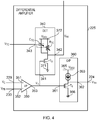
- Figure 4 illustrates an embodiment of the differential amplifier 225 showing an example embodiment the detector stage 340 and an example embodiment of the output stage 360.
- the detector stage 340 comprises a transistor T 5 having a drain coupled to the output 342 of the detector stage 340, a source coupled to a power supply rail 371, which may be ground, and a gate coupled to the first input 341 of the detector stage 340.
- a variable capacitance element C TC is coupled between the output 342 of the detector stage 340 and a power supply rail 372 at a voltage V DD1 .
- a variable resistance element R TC is also coupled between the output 342 of the detector stage 340 and the power supply rail 372.
- the capacitance of the variable capacitance element C TC and the resistance of the variable resistance element R TC is adjustable by means of the time constant control signal V TC present at the second input 343 of the detector stage 340.
- the output stage 360 comprises a transistor T 6 having a drain coupled to the output 362 of the output stage 360, a source coupled to a power supply rail 366, which may be ground, and a gate coupled to the input 361 of the output stage 360.
- a current source 363 is coupled between the output 362 of the output stage 360 and a power supply rail 365 at the voltage V DD2 .
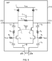
- Figure 5 illustrates an embodiment of the amplifier circuit 210 suitable for use in RFICs.
- first and second transistors T 1 , T 2 are configured as a cascode pair coupled between the first signal output 212 and ground 2, with the first transistor T 1 being an upper transistor and the second transistor T 2 being a lower transistor.
- a first bias voltage V BIAS1 is applied to a gate of the first transistor T 1 .
- a first inductive element L 1 is coupled between the first signal output 212 and a power supply rail 1 at a voltage V DD3 .
- a first capacitive element C 1 is coupled between the first signal output 212 and the second signal output 213.
- a first resistive element R 1 is also coupled between the first signal output 212 and the second signal output 213, and is a model of the loading of subsequent circuit blocks coupled to the first and second signal outputs 212, 213.
- a second bias voltage V BIAS2 is applied to a gate of the second transistor T 2 via a second resistive element R 2 .
- a second capacitive element C 2 is coupled in series with a third resistive element R 3 between the first signal output 212 and the gate of the second transistor T 2 .
- a third capacitive element C 3 is coupled between the gate of the second transistor T 2 and the first signal input 208, thereby providing AC coupling of the first input signal component V i+ .
- Third and fourth transistors T 3 , T 4 are configured as a cascode pair coupled between the second signal output 213 and ground 2, with the third transistor T 3 being an upper transistor and the fourth transistor T 4 being a lower transistor.
- the second and fourth transistors T 2 , T 4 form a common-source differential pair.
- the first and third transistors T 1 , T 3 form cascode transistors for isolating the signal input 211 from the first and second signal outputs 212, 213.
- a first bias voltage V BIAS1 is applied to a gate of the third transistor T 3 .
- a second inductive element L 2 is coupled between the second signal output 213 and the power supply rail 1 at the voltage V DD3 .
- the second bias voltage V BIAS2 is applied to a gate of the fourth transistor T 4 via a fourth resistive element R 4 .
- a fourth capacitive element C 4 is coupled in series with a fifth resistive element R 5 between the second signal output 213 and the gate of the fourth transistor T 4 .
- a fifth capacitive element C 5 is coupled between the gate of the fourth transistor T 4 and the second signal input 209, thereby providing AC coupling of the second input signal component V i- .
- the first and second inductive elements L 1 , L 2 in conjunction with the first capacitive element C 1 constitute a resonator load and enable high output impedance of the amplifier circuit 210.
- the resonator load is tuneable by varying the capacitance of the first capacitive element C 1 , which can contribute to extending the bandwidth of the amplifier circuit 210, and can contribute to suppressing unwanted interference having a frequency three times the frequency of the wanted input signal V i , prior to down conversion of the amplified input signal V i in a subsequent stage.
- Resistive feedback provided by the third and fifth resistive elements R 3 , R 5 determines the input impedance of the amplifier circuit 210.
- This impedance may be represented as (R 3 +R 5 )/(G+1), where R 3 and R 5 represent the resistance of the third and fifth resistive elements R 3 , R 5 , and G represents the voltage gain of the amplifier circuit 210.
- the third and fifth resistive elements R 3 , R 5 are large, with low noise contribution.
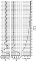
- Figure 6 is a graph showing voltages varying with time.
- trace a) shows the threshold signal V TH , which is the voltage across the capacitive element 226 of the amplification device 200 illustrated in Figure 2 , when the level of the input signal V i is increased at time zero, for example by the addition of an interfering signal to a wanted signal.
- Trace a) exhibits some fast ringing, caused by the rectified interfering signal, superimposed on a slower variation.
- the difference signal V ⁇ After some initial ringing, the difference signal V ⁇ reaches steady state after about 10ns, at which point the average current injected via the first and second diodes 221, 235 is counteracted by the current in the transistor T 6 Trace c) shows the averaged signal V AV generated by the detector stage 340 and which corresponds to an averaged, by low pass filtering, replica of a voltage at the output 362 of the output stage 360.
- the time constant for the averaging by the detector stage 340 is arranged to be higher than a response time of the differential input stage 350. Consequently, the averaged signal V AV reaches steady state more slowly than the difference signal V ⁇ , after about 20ns.
- a receiving apparatus 400 comprises an antenna 410 coupled to an input 422 of a receiver 420.
- An output 424 of the receiver 420 is coupled to an input 432 of a digital signal processor (DSP) 430.
- the receiver 420 comprises the amplification device 100 described with reference to Figure 1 , or alternatively may comprise the amplification device 200 or 300 described with reference to Figures 2 and 3 respectively.
- the input 422 of the receiver 420 is coupled to the signal input 111 of the amplification device 100 for receiving the input signal V i to be amplified, which is a signal detected by the antenna 410.
- the amplification device 100 provides low noise amplification of the input signal V i detected by the antenna 410.
- the receiver 420 also comprises a mixer 428, a local oscillator signal generator (LO) 430, a filter 440, and an analogue to digital converter (ADC) 450.
- the first signal output 112 of the amplification device 100, and also the second signal output 113 if the amplification device 200 or 300 is alternatively employed, is coupled to a signal input 422 of the mixer 428.
- the local oscillator signal generator (LO) 430 is coupled to an oscillator input 424 of the mixer 428 for delivering a local oscillator signal.
- the mixer 428 down-converts the input signal V i after amplification by the amplification device 100, and delivers a down-converted signal at an output 426 of the mixer 428.
- the output 426 of the mixer 428 is coupled to an input 442 of the filter 440 for filtering the down-converted signal, and an output 444 of the filter 440 is coupled to the output 424 of the receiver 420 by means of the ADC 450.
- the digitised signal is processed by the DSP 430 to extract information conveyed by the input signal V i .
- the DSP 430 may be arranged to determine a signal-to-interference ratio of the first and/or second output signals V O+ , V O- after demodulation, and may comprise an optional output 431 coupled to the input 371 of the time constant controller 370 for delivering an indication of signal-to-interference ratio.
- a radio communication apparatus 500 comprises the elements of the receiving apparatus 400 described with reference to Figure 7 , and additionally comprises a transmitter 540 coupled between an output 434 of the DSP 430 and the antenna 410 for transmitting a signal generated by the DSP 430.
- the amplifier circuit 210 may be arranged to amplify an input signal V i that is a single ended signal, in which case the amplifier circuit 210 has a single input for receiving a single ended input signal.
Landscapes
- Engineering & Computer Science (AREA)
- Power Engineering (AREA)
- Computer Networks & Wireless Communication (AREA)
- Signal Processing (AREA)
- Amplifiers (AREA)
Claims (15)
- Verstärkungsvorrichtung (100), umfassend:eine Verstärkerschaltung (110) und einen Begrenzer (120);wobei die Verstärkerschaltung (110) einen Signaleingang (111) für ein zu verstärkendes Eingangssignal umfasst und einen ersten Signalausgang (112) für ein erstes Ausgangssignal; undwobei der Begrenzer (120) umfasst:einen Differenzverstärker (125), der einen ersten Differenzverstärkereingang (129) für ein Schwellenwertsteuersignal, einen zweiten Differenzverstärkereingang (113) für ein Rückkopplungssignal und einen Differenzverstärkerausgang (124) für ein Schwellenwertsignal umfasst, das indikativ für eine Differenz zwischen dem Schwellenwertsteuersignal und dem Rückkopplungssignal ist;eine erste Diode (121) mit einer ersten Anode (122), die mit dem ersten Signalausgang (112) gekoppelt ist, und eine erste Kathode (123), die mit dem Differenzverstärkerausgang (124) gekoppelt ist; undeine Rückkopplungsstufe (128), die zwischen dem Differenzverstärkerausgang (124) und dem zweiten Differenzverstärkereingang (130) gekoppelt ist, wobei die Rückkopplungsstufe (128) angeordnet ist, das Rückkopplungssignal in Abhängigkeit von dem Schwellenwertsignal zu erzeugen.
- Verstärkungsvorrichtung (100) nach Anspruch 1, wobei der Begrenzer (120) eine Schwellenwertsteuerer (134) umfasst, die angeordnet ist, das Schwellenwertsteuersignal in Abhängigkeit von einer Eigenschaft der Verstärkerschaltung (110) zu erzeugen.
- Verstärkungsvorrichtung (100) nach Anspruch 2, wobei die Eigenschaft der Verstärkerschaltung (110) Temperatur der Verstärkerschaltung (110) ist.
- Verstärkervorrichtung (300) nach einem der vorstehenden Ansprüche, wobei:der Differenzverstärker (225) eine Detektorstufe (340) umfasst, die angeordnet ist, ein gemitteltes Signal zu erzeugen, das indikativ für einen Mittelwert einer Differenz zwischen dem Schwellenwertsteuersignal und dem Rückkopplungssignal ist;die Verstärkungsvorrichtung (300) ferner eine Verstärkungssteuerungsstufe (345) umfasst, die angeordnet ist, ein Verstärkungssteuersignal in Abhängigkeit von dem gemittelten Signal zu erzeugen; unddie Verstärkereinheit (110) angeordnet ist, eine Verstärkung in Abhängigkeit von dem Verstärkungssteuersignal aufzuweisen.
- Verstärkungsvorrichtung (300) nach Anspruch 4, wobei die Verstärkungssteuerungsstufe (345) angeordnet ist, das Verstärkungssteuersignal derart zu steuern, dass die Verstärkung der Verstärkerschaltung (110) als Reaktion darauf, dass das gemittelte Signal indikativ dafür ist, dass das Eingangssignal einen Pegel unter einem unteren Signalpegelschwellenwert aufweist, erhöht wird, in Reaktion darauf, dass das gemittelte Signal indikativ dafür ist, dass das Eingangssignal einen Pegel über einem oberen Signalpegelschwellenwert hat, verringert wird, und in Reaktion darauf, dass das gemittelte Signal indikativ dafür ist, dass das Eingangssignal einen Pegel hat, der zwischen dem unteren Signalpegelschwellenwert und dem oberen Signalpegelschwellenwert liegt, unverändert bleibt.
- Verstärkungsvorrichtung (300) nach Anspruch 4 oder Anspruch 5, wobei die Detektorstufe (340) angeordnet ist, eine einstellbare Zeitkonstante zum Erzeugen des gemittelten Signals einzusetzen, und wobei der Begrenzer (220) ferner eine Zeitkonstantensteuerer (370) umfasst, die mit der Detektorstufe (340) gekoppelt und angeordnet ist, um die einstellbare Zeitkonstante in Abhängigkeit von einer Eigenschaft des zu verstärkenden Eingangssignals einzustellen.
- Verstärkungsvorrichtung (300) nach einem der Ansprüche 4 bis 6, wobei:der Differenzverstärker (225) eine Differenzeingangsstufe (350) und eine Ausgangsstufe (360) umfasst, wobei ein erster Eingang (351) der Differenzeingangsstufe (350) mit dem ersten Differenzverstärkereingang (229) gekoppelt ist und ein zweiter Eingang (352) der Differenzeingangsstufe (350) mit dem zweiten Differenzverstärkereingang (230) gekoppelt ist, wobei ein Eingang (361) der Ausgangsstufe (360) mit einem Ausgang (353) der Differenzeingangsstufe (350) gekoppelt ist und ein Ausgang (362) der Ausgangsstufe (360) mit dem Differenzausgang (224) des Differenzverstärkers (225) gekoppelt ist; unddie Detektorstufe (340) mit dem Ausgang (353) der Differenzeingangsstufe (350) zum Bestimmen des gemittelten Signals gekoppelt ist.
- Verstärkungsvorrichtung (300) nach einem der Ansprüche 4 bis 7, wobei die Detektorstufe (340) angeordnet ist, um einen Strom, der in der Ausgangsstufe (360) fließt, durch Erzeugen eines Stroms proportional zu einem Strom, der in der Ausgangsstufe (360) fließt, zu replizieren, und angeordnet ist, um das gemittelte Signal aus dem Replikat zu erzeugen.
- Verstärkungsvorrichtung (200) nach einem der vorstehenden Ansprüche, wobei die Verstärkerschaltung (210) einen zweiten Signalausgang (213) für ein zweites Ausgangssignal umfasst, wobei das erste und das zweite Ausgangssignal zusammen ein Differenzsignal bilden, und wobei der Begrenzer (220) eine zweite Diode (235) umfasst, die eine zweite Anode (236) aufweist, die mit dem zweiten Signalausgang (213) gekoppelt ist, und eine zweite Kathode (237), die mit dem Differenzverstärkerausgang (224) gekoppelt ist.
- Verstärkungsvorrichtung (200) nach einem der vorstehenden Ansprüche, wobei die Rückkopplungsstufe (228) ein kapazitives Element (226) aufweist, das zwischen dem Differenzverstärkerausgang (224) und einer ersten Spannungsversorgungsschiene (227) gekoppelt ist.
- Verstärkungsvorrichtung (200) nach einem der vorstehenden Ansprüche, wobei die Rückkopplungsstufe (228) umfasst:ein erstes widerstandsbehaftetes Element (231), das zwischen dem Differenzverstärkerausgang (224) und dem zweiten Differenzverstärkereingang (230) gekoppelt ist; undein zweites widerstandsbehaftetes Element (232), das zwischen dem zweiten Differenzverstärkereingang (230) und einer zweiten Stromversorgungsschiene (233) gekoppelt ist.
- Verstärkungsvorrichtung (100) nach einem der vorstehenden Ansprüche, wobei die Verstärkerschaltung (110) ein rauscharmer Verstärker, LNA, (Low Noise Amplifier) ist.
- Empfangende Vorrichtung (400), eine Verstärkungsvorrichtung (100) nach einem der vorstehenden Ansprüche umfassend.
- Funkkommunikationsvorrichtung (500), eine empfangende Vorrichtung (400) nach Anspruch 13 umfassend.
- Funkkommunikationsvorrichtung (500) nach Anspruch 14, wobei die Funkkommunikationsvorrichtung (500) eine Basisstation ist.
Applications Claiming Priority (1)
| Application Number | Priority Date | Filing Date | Title |
|---|---|---|---|
| PCT/EP2015/072890 WO2017059880A1 (en) | 2015-10-05 | 2015-10-05 | Amplification device incorporating limiting |
Publications (2)
| Publication Number | Publication Date |
|---|---|
| EP3360249A1 EP3360249A1 (de) | 2018-08-15 |
| EP3360249B1 true EP3360249B1 (de) | 2019-08-14 |
Family
ID=54329507
Family Applications (1)
| Application Number | Title | Priority Date | Filing Date |
|---|---|---|---|
| EP15781317.1A Active EP3360249B1 (de) | 2015-10-05 | 2015-10-05 | Amplifikationsvorrichtung mit begrenzung |
Country Status (4)
| Country | Link |
|---|---|
| US (1) | US10171043B2 (de) |
| EP (1) | EP3360249B1 (de) |
| CN (1) | CN108141185B (de) |
| WO (1) | WO2017059880A1 (de) |
Families Citing this family (6)
| Publication number | Priority date | Publication date | Assignee | Title |
|---|---|---|---|---|
| US9887673B2 (en) * | 2016-03-11 | 2018-02-06 | Intel Corporation | Ultra compact multi-band transmitter with robust AM-PM distortion self-suppression techniques |
| DE102016124962B4 (de) * | 2016-12-20 | 2024-10-24 | Infineon Technologies Ag | Speichervorrichtung und Verfahren zum Steuern einer Speicherunterstützungsfunktion |
| US11283479B2 (en) | 2020-06-18 | 2022-03-22 | Analog Devices, Inc. | Apparatus and methods for radio frequency signal limiting |
| WO2022226935A1 (zh) * | 2021-04-29 | 2022-11-03 | 华为技术有限公司 | 射频集成电路芯片和无线通信装置 |
| US12003268B2 (en) * | 2021-05-28 | 2024-06-04 | Skyworks Solutions, Inc. | Apparatus and methods for power amplifier signal limiting |
| US12483206B2 (en) | 2023-03-09 | 2025-11-25 | Analog Devices, Inc. | Broadband low noise amplifiers with integrated limiters and fast recovery time |
Family Cites Families (33)
| Publication number | Priority date | Publication date | Assignee | Title |
|---|---|---|---|---|
| US3666970A (en) * | 1971-03-15 | 1972-05-30 | Gte Sylvania Inc | Limiter circuit |
| US3944167A (en) * | 1973-08-24 | 1976-03-16 | Sanders Associates, Inc. | Radiation detection apparatus |
| US3991370A (en) * | 1975-10-03 | 1976-11-09 | John Pate | Peak limiter |
| KR0141495B1 (ko) * | 1988-11-01 | 1998-07-15 | 미다 가쓰시게 | 반도체 기억장치 및 그 결함구제방법 |
| KR0168404B1 (ko) * | 1990-12-06 | 1999-03-20 | 오오가 노리오 | 피드백 클램프 회로 |
| JPH04227123A (ja) * | 1990-12-29 | 1992-08-17 | Nec Corp | 無線通信装置 |
| US5771301A (en) * | 1994-09-15 | 1998-06-23 | John D. Winslett | Sound leveling system using output slope control |
| FR2745666B1 (fr) * | 1996-02-29 | 1998-05-22 | Sgs Thomson Microelectronics | Circuit de reglage de gain automatique utilisant un condensateur pour reduire le couplage de bruit numerique |
| CN1178413A (zh) * | 1996-09-20 | 1998-04-08 | 诺基亚流动电话有限公司 | 放大器系统 |
| US5737432A (en) * | 1996-11-18 | 1998-04-07 | Aphex Systems, Ltd. | Split-band clipper |
| JPH10173456A (ja) * | 1996-12-11 | 1998-06-26 | Fujitsu Ltd | 信号増幅回路 |
| US5973561A (en) | 1997-06-03 | 1999-10-26 | Texas Instruments Incorporated | Differential clamp for amplifier circuits |
| TW444477B (en) * | 1997-08-12 | 2001-07-01 | Klaus Wolter | A device for converting small currents impressed at the input of the device by a non-ideal source of current, into voltage signals |
| GB2343943B (en) * | 1998-11-18 | 2003-11-26 | Ericsson Telefon Ab L M | Detection circuit |
| EP1304886A1 (de) * | 2001-10-10 | 2003-04-23 | Deutsche Thomson-Brandt Gmbh | Unterdrückung von Sättigung im Signalverstärker einer Kathodenstrahlröhre |
| US6762647B1 (en) * | 2002-08-09 | 2004-07-13 | Triquint Semiconductor, Inc. | Active protection circuit for load mismatched power amplifier |
| JP4311034B2 (ja) * | 2003-02-14 | 2009-08-12 | 沖電気工業株式会社 | 帯域復元装置及び電話機 |
| US7280330B2 (en) * | 2004-09-08 | 2007-10-09 | Texas Instruments Incorporated | ESD protection for RF power amplifier circuits |
| US7202749B2 (en) * | 2004-09-27 | 2007-04-10 | Broadcom Corporation | AC coupling technique for improved noise performance and simple biasing |
| US7583904B2 (en) * | 2006-06-12 | 2009-09-01 | Broadlight Ltd. | Transimpedance (TIA) circuit usable for burst mode communications |
| JP5138990B2 (ja) * | 2007-06-28 | 2013-02-06 | ラピスセミコンダクタ株式会社 | 前置増幅器および光受信装置 |
| US8330520B2 (en) * | 2008-06-09 | 2012-12-11 | Shimadzu Corporation | Limiter circuit |
| US9660590B2 (en) * | 2008-07-18 | 2017-05-23 | Peregrine Semiconductor Corporation | Low-noise high efficiency bias generation circuits and method |
| JP5228840B2 (ja) * | 2008-11-27 | 2013-07-03 | ヤマハ株式会社 | 増幅器 |
| SE534502C2 (sv) * | 2009-09-14 | 2011-09-13 | Abletec As | Effektförstärkare |
| US8369818B2 (en) | 2011-06-27 | 2013-02-05 | Broadcom Corporation | Low noise amplifier protection using a clamping device |
| DE202011103692U1 (de) * | 2011-07-25 | 2011-09-30 | Thomas Strauss | Signalverstärker mit Amplitudenbegrenzung |
| US9124084B2 (en) * | 2011-11-03 | 2015-09-01 | Intel Corporation | Charge injection and drain-based electrical overstress (EOS) protection apparatus and method |
| EP2632173B1 (de) * | 2012-02-22 | 2015-06-03 | Harman Becker Automotive Systems GmbH | Lautsprecherüberlastungsschutz |
| JP5982065B2 (ja) * | 2012-10-01 | 2016-08-31 | テレフオンアクチーボラゲット エルエム エリクソン(パブル) | Aas送信機歪みの改善 |
| US8712066B1 (en) * | 2013-03-14 | 2014-04-29 | Rockford Corporation | Audio signal clip detection |
| CN103762963A (zh) | 2014-01-16 | 2014-04-30 | 四川和芯微电子股份有限公司 | 快速比较电路 |
| US9628195B2 (en) * | 2014-10-22 | 2017-04-18 | Source Photonics (Chengdu) Co., Ltd. | Transimpedance amplifier (TIA) having an enlarged dynamic range and optical devices using the same |
-
2015
- 2015-10-05 US US15/763,861 patent/US10171043B2/en active Active
- 2015-10-05 CN CN201580083688.7A patent/CN108141185B/zh active Active
- 2015-10-05 WO PCT/EP2015/072890 patent/WO2017059880A1/en not_active Ceased
- 2015-10-05 EP EP15781317.1A patent/EP3360249B1/de active Active
Non-Patent Citations (1)
| Title |
|---|
| None * |
Also Published As
| Publication number | Publication date |
|---|---|
| CN108141185A (zh) | 2018-06-08 |
| EP3360249A1 (de) | 2018-08-15 |
| WO2017059880A1 (en) | 2017-04-13 |
| US20180287570A1 (en) | 2018-10-04 |
| US10171043B2 (en) | 2019-01-01 |
| CN108141185B (zh) | 2021-08-03 |
Similar Documents
| Publication | Publication Date | Title |
|---|---|---|
| US10171043B2 (en) | Amplification device incorporating limiting | |
| EP2470918B1 (de) | Hochlinearer schneller spitzenwertdetektor | |
| EP1897216B1 (de) | Automatische bias-kontrollschaltung für lineare leistungsverstärker | |
| US10348248B2 (en) | Power amplifier module | |
| JP5854372B2 (ja) | 電力増幅モジュール | |
| US7352244B2 (en) | Electronics parts for high frequency power amplifier | |
| US9660589B2 (en) | Power amplifier module | |
| US8432228B1 (en) | Power control circuit for radio frequency power amplifiers | |
| US20170141734A1 (en) | Circuits and methods for controlling power amplifiers | |
| US20160315594A1 (en) | Power amplification module | |
| US20150188496A1 (en) | Gate bias control circuit and power amplifying device having the same | |
| US20150105032A1 (en) | Dynamic bias to improve switch linearity | |
| US9641128B2 (en) | High linearity structure for amplifier | |
| KR101101560B1 (ko) | 전력 증폭기 | |
| US12095426B2 (en) | Amplifier and signal processing apparatus | |
| JP2016158152A (ja) | 半導体装置 | |
| HK1218470A1 (zh) | 通過射頻輸入信號的幅度調整的壓縮控制 | |
| HK1218470B (en) | Compression control through amplitude adjustment of a radio frequency input signal | |
| HK1218469B (en) | Compression control through power amplifier voltage adjustment |
Legal Events
| Date | Code | Title | Description |
|---|---|---|---|
| STAA | Information on the status of an ep patent application or granted ep patent |
Free format text: STATUS: THE INTERNATIONAL PUBLICATION HAS BEEN MADE |
|
| PUAI | Public reference made under article 153(3) epc to a published international application that has entered the european phase |
Free format text: ORIGINAL CODE: 0009012 |
|
| STAA | Information on the status of an ep patent application or granted ep patent |
Free format text: STATUS: REQUEST FOR EXAMINATION WAS MADE |
|
| 17P | Request for examination filed |
Effective date: 20180404 |
|
| AK | Designated contracting states |
Kind code of ref document: A1 Designated state(s): AL AT BE BG CH CY CZ DE DK EE ES FI FR GB GR HR HU IE IS IT LI LT LU LV MC MK MT NL NO PL PT RO RS SE SI SK SM TR |
|
| AX | Request for extension of the european patent |
Extension state: BA ME |
|
| DAV | Request for validation of the european patent (deleted) | ||
| DAX | Request for extension of the european patent (deleted) | ||
| GRAP | Despatch of communication of intention to grant a patent |
Free format text: ORIGINAL CODE: EPIDOSNIGR1 |
|
| STAA | Information on the status of an ep patent application or granted ep patent |
Free format text: STATUS: GRANT OF PATENT IS INTENDED |
|
| RIC1 | Information provided on ipc code assigned before grant |
Ipc: H03G 3/30 20060101ALI20190411BHEP Ipc: H03F 3/45 20060101ALI20190411BHEP Ipc: H03F 1/52 20060101AFI20190411BHEP Ipc: H04B 1/16 20060101ALI20190411BHEP Ipc: H03F 3/189 20060101ALI20190411BHEP Ipc: H03F 3/193 20060101ALI20190411BHEP |
|
| INTG | Intention to grant announced |
Effective date: 20190507 |
|
| GRAS | Grant fee paid |
Free format text: ORIGINAL CODE: EPIDOSNIGR3 |
|
| GRAA | (expected) grant |
Free format text: ORIGINAL CODE: 0009210 |
|
| STAA | Information on the status of an ep patent application or granted ep patent |
Free format text: STATUS: THE PATENT HAS BEEN GRANTED |
|
| AK | Designated contracting states |
Kind code of ref document: B1 Designated state(s): AL AT BE BG CH CY CZ DE DK EE ES FI FR GB GR HR HU IE IS IT LI LT LU LV MC MK MT NL NO PL PT RO RS SE SI SK SM TR |
|
| REG | Reference to a national code |
Ref country code: GB Ref legal event code: FG4D |
|
| REG | Reference to a national code |
Ref country code: CH Ref legal event code: EP Ref country code: AT Ref legal event code: REF Ref document number: 1168211 Country of ref document: AT Kind code of ref document: T Effective date: 20190815 |
|
| REG | Reference to a national code |
Ref country code: IE Ref legal event code: FG4D |
|
| REG | Reference to a national code |
Ref country code: DE Ref legal event code: R096 Ref document number: 602015035889 Country of ref document: DE |
|
| REG | Reference to a national code |
Ref country code: NL Ref legal event code: MP Effective date: 20190814 |
|
| REG | Reference to a national code |
Ref country code: LT Ref legal event code: MG4D |
|
| PG25 | Lapsed in a contracting state [announced via postgrant information from national office to epo] |
Ref country code: LT Free format text: LAPSE BECAUSE OF FAILURE TO SUBMIT A TRANSLATION OF THE DESCRIPTION OR TO PAY THE FEE WITHIN THE PRESCRIBED TIME-LIMIT Effective date: 20190814 Ref country code: HR Free format text: LAPSE BECAUSE OF FAILURE TO SUBMIT A TRANSLATION OF THE DESCRIPTION OR TO PAY THE FEE WITHIN THE PRESCRIBED TIME-LIMIT Effective date: 20190814 Ref country code: NL Free format text: LAPSE BECAUSE OF FAILURE TO SUBMIT A TRANSLATION OF THE DESCRIPTION OR TO PAY THE FEE WITHIN THE PRESCRIBED TIME-LIMIT Effective date: 20190814 Ref country code: BG Free format text: LAPSE BECAUSE OF FAILURE TO SUBMIT A TRANSLATION OF THE DESCRIPTION OR TO PAY THE FEE WITHIN THE PRESCRIBED TIME-LIMIT Effective date: 20191114 Ref country code: SE Free format text: LAPSE BECAUSE OF FAILURE TO SUBMIT A TRANSLATION OF THE DESCRIPTION OR TO PAY THE FEE WITHIN THE PRESCRIBED TIME-LIMIT Effective date: 20190814 Ref country code: NO Free format text: LAPSE BECAUSE OF FAILURE TO SUBMIT A TRANSLATION OF THE DESCRIPTION OR TO PAY THE FEE WITHIN THE PRESCRIBED TIME-LIMIT Effective date: 20191114 Ref country code: FI Free format text: LAPSE BECAUSE OF FAILURE TO SUBMIT A TRANSLATION OF THE DESCRIPTION OR TO PAY THE FEE WITHIN THE PRESCRIBED TIME-LIMIT Effective date: 20190814 Ref country code: PT Free format text: LAPSE BECAUSE OF FAILURE TO SUBMIT A TRANSLATION OF THE DESCRIPTION OR TO PAY THE FEE WITHIN THE PRESCRIBED TIME-LIMIT Effective date: 20191216 |
|
| REG | Reference to a national code |
Ref country code: AT Ref legal event code: MK05 Ref document number: 1168211 Country of ref document: AT Kind code of ref document: T Effective date: 20190814 |
|
| PG25 | Lapsed in a contracting state [announced via postgrant information from national office to epo] |
Ref country code: RS Free format text: LAPSE BECAUSE OF FAILURE TO SUBMIT A TRANSLATION OF THE DESCRIPTION OR TO PAY THE FEE WITHIN THE PRESCRIBED TIME-LIMIT Effective date: 20190814 Ref country code: IS Free format text: LAPSE BECAUSE OF FAILURE TO SUBMIT A TRANSLATION OF THE DESCRIPTION OR TO PAY THE FEE WITHIN THE PRESCRIBED TIME-LIMIT Effective date: 20191214 Ref country code: GR Free format text: LAPSE BECAUSE OF FAILURE TO SUBMIT A TRANSLATION OF THE DESCRIPTION OR TO PAY THE FEE WITHIN THE PRESCRIBED TIME-LIMIT Effective date: 20191115 Ref country code: LV Free format text: LAPSE BECAUSE OF FAILURE TO SUBMIT A TRANSLATION OF THE DESCRIPTION OR TO PAY THE FEE WITHIN THE PRESCRIBED TIME-LIMIT Effective date: 20190814 Ref country code: AL Free format text: LAPSE BECAUSE OF FAILURE TO SUBMIT A TRANSLATION OF THE DESCRIPTION OR TO PAY THE FEE WITHIN THE PRESCRIBED TIME-LIMIT Effective date: 20190814 Ref country code: ES Free format text: LAPSE BECAUSE OF FAILURE TO SUBMIT A TRANSLATION OF THE DESCRIPTION OR TO PAY THE FEE WITHIN THE PRESCRIBED TIME-LIMIT Effective date: 20190814 |
|
| PG25 | Lapsed in a contracting state [announced via postgrant information from national office to epo] |
Ref country code: TR Free format text: LAPSE BECAUSE OF FAILURE TO SUBMIT A TRANSLATION OF THE DESCRIPTION OR TO PAY THE FEE WITHIN THE PRESCRIBED TIME-LIMIT Effective date: 20190814 |
|
| PG25 | Lapsed in a contracting state [announced via postgrant information from national office to epo] |
Ref country code: RO Free format text: LAPSE BECAUSE OF FAILURE TO SUBMIT A TRANSLATION OF THE DESCRIPTION OR TO PAY THE FEE WITHIN THE PRESCRIBED TIME-LIMIT Effective date: 20190814 Ref country code: IT Free format text: LAPSE BECAUSE OF FAILURE TO SUBMIT A TRANSLATION OF THE DESCRIPTION OR TO PAY THE FEE WITHIN THE PRESCRIBED TIME-LIMIT Effective date: 20190814 Ref country code: EE Free format text: LAPSE BECAUSE OF FAILURE TO SUBMIT A TRANSLATION OF THE DESCRIPTION OR TO PAY THE FEE WITHIN THE PRESCRIBED TIME-LIMIT Effective date: 20190814 Ref country code: DK Free format text: LAPSE BECAUSE OF FAILURE TO SUBMIT A TRANSLATION OF THE DESCRIPTION OR TO PAY THE FEE WITHIN THE PRESCRIBED TIME-LIMIT Effective date: 20190814 Ref country code: AT Free format text: LAPSE BECAUSE OF FAILURE TO SUBMIT A TRANSLATION OF THE DESCRIPTION OR TO PAY THE FEE WITHIN THE PRESCRIBED TIME-LIMIT Effective date: 20190814 Ref country code: PL Free format text: LAPSE BECAUSE OF FAILURE TO SUBMIT A TRANSLATION OF THE DESCRIPTION OR TO PAY THE FEE WITHIN THE PRESCRIBED TIME-LIMIT Effective date: 20190814 |
|
| PG25 | Lapsed in a contracting state [announced via postgrant information from national office to epo] |
Ref country code: SM Free format text: LAPSE BECAUSE OF FAILURE TO SUBMIT A TRANSLATION OF THE DESCRIPTION OR TO PAY THE FEE WITHIN THE PRESCRIBED TIME-LIMIT Effective date: 20190814 Ref country code: CZ Free format text: LAPSE BECAUSE OF FAILURE TO SUBMIT A TRANSLATION OF THE DESCRIPTION OR TO PAY THE FEE WITHIN THE PRESCRIBED TIME-LIMIT Effective date: 20190814 Ref country code: SK Free format text: LAPSE BECAUSE OF FAILURE TO SUBMIT A TRANSLATION OF THE DESCRIPTION OR TO PAY THE FEE WITHIN THE PRESCRIBED TIME-LIMIT Effective date: 20190814 Ref country code: MC Free format text: LAPSE BECAUSE OF FAILURE TO SUBMIT A TRANSLATION OF THE DESCRIPTION OR TO PAY THE FEE WITHIN THE PRESCRIBED TIME-LIMIT Effective date: 20190814 Ref country code: IS Free format text: LAPSE BECAUSE OF FAILURE TO SUBMIT A TRANSLATION OF THE DESCRIPTION OR TO PAY THE FEE WITHIN THE PRESCRIBED TIME-LIMIT Effective date: 20200224 |
|
| REG | Reference to a national code |
Ref country code: CH Ref legal event code: PL |
|
| REG | Reference to a national code |
Ref country code: DE Ref legal event code: R097 Ref document number: 602015035889 Country of ref document: DE |
|
| PLBE | No opposition filed within time limit |
Free format text: ORIGINAL CODE: 0009261 |
|
| STAA | Information on the status of an ep patent application or granted ep patent |
Free format text: STATUS: NO OPPOSITION FILED WITHIN TIME LIMIT |
|
| PG2D | Information on lapse in contracting state deleted |
Ref country code: IS |
|
| PG25 | Lapsed in a contracting state [announced via postgrant information from national office to epo] |
Ref country code: LI Free format text: LAPSE BECAUSE OF NON-PAYMENT OF DUE FEES Effective date: 20191031 Ref country code: CH Free format text: LAPSE BECAUSE OF NON-PAYMENT OF DUE FEES Effective date: 20191031 Ref country code: LU Free format text: LAPSE BECAUSE OF NON-PAYMENT OF DUE FEES Effective date: 20191005 |
|
| 26N | No opposition filed |
Effective date: 20200603 |
|
| REG | Reference to a national code |
Ref country code: BE Ref legal event code: MM Effective date: 20191031 |
|
| PG25 | Lapsed in a contracting state [announced via postgrant information from national office to epo] |
Ref country code: SI Free format text: LAPSE BECAUSE OF FAILURE TO SUBMIT A TRANSLATION OF THE DESCRIPTION OR TO PAY THE FEE WITHIN THE PRESCRIBED TIME-LIMIT Effective date: 20190814 Ref country code: BE Free format text: LAPSE BECAUSE OF NON-PAYMENT OF DUE FEES Effective date: 20191031 |
|
| PG25 | Lapsed in a contracting state [announced via postgrant information from national office to epo] |
Ref country code: FR Free format text: LAPSE BECAUSE OF NON-PAYMENT OF DUE FEES Effective date: 20191014 Ref country code: IE Free format text: LAPSE BECAUSE OF NON-PAYMENT OF DUE FEES Effective date: 20191005 |
|
| PG25 | Lapsed in a contracting state [announced via postgrant information from national office to epo] |
Ref country code: CY Free format text: LAPSE BECAUSE OF FAILURE TO SUBMIT A TRANSLATION OF THE DESCRIPTION OR TO PAY THE FEE WITHIN THE PRESCRIBED TIME-LIMIT Effective date: 20190814 |
|
| PG25 | Lapsed in a contracting state [announced via postgrant information from national office to epo] |
Ref country code: MT Free format text: LAPSE BECAUSE OF FAILURE TO SUBMIT A TRANSLATION OF THE DESCRIPTION OR TO PAY THE FEE WITHIN THE PRESCRIBED TIME-LIMIT Effective date: 20190814 Ref country code: HU Free format text: LAPSE BECAUSE OF FAILURE TO SUBMIT A TRANSLATION OF THE DESCRIPTION OR TO PAY THE FEE WITHIN THE PRESCRIBED TIME-LIMIT; INVALID AB INITIO Effective date: 20151005 |
|
| PG25 | Lapsed in a contracting state [announced via postgrant information from national office to epo] |
Ref country code: MK Free format text: LAPSE BECAUSE OF FAILURE TO SUBMIT A TRANSLATION OF THE DESCRIPTION OR TO PAY THE FEE WITHIN THE PRESCRIBED TIME-LIMIT Effective date: 20190814 |
|
| PGFP | Annual fee paid to national office [announced via postgrant information from national office to epo] |
Ref country code: DE Payment date: 20251029 Year of fee payment: 11 |
|
| PGFP | Annual fee paid to national office [announced via postgrant information from national office to epo] |
Ref country code: GB Payment date: 20251027 Year of fee payment: 11 |