EP3364237A1 - Anzeigetafel und herstellungsverfahren dafür - Google Patents
Anzeigetafel und herstellungsverfahren dafür Download PDFInfo
- Publication number
- EP3364237A1 EP3364237A1 EP16834013.1A EP16834013A EP3364237A1 EP 3364237 A1 EP3364237 A1 EP 3364237A1 EP 16834013 A EP16834013 A EP 16834013A EP 3364237 A1 EP3364237 A1 EP 3364237A1
- Authority
- EP
- European Patent Office
- Prior art keywords
- liquid crystal
- display panel
- layer
- polymerizable monomers
- electrode
- Prior art date
- Legal status (The legal status is an assumption and is not a legal conclusion. Google has not performed a legal analysis and makes no representation as to the accuracy of the status listed.)
- Granted
Links
Images



Classifications
-
- G—PHYSICS
- G02—OPTICS
- G02F—OPTICAL DEVICES OR ARRANGEMENTS FOR THE CONTROL OF LIGHT BY MODIFICATION OF THE OPTICAL PROPERTIES OF THE MEDIA OF THE ELEMENTS INVOLVED THEREIN; NON-LINEAR OPTICS; FREQUENCY-CHANGING OF LIGHT; OPTICAL LOGIC ELEMENTS; OPTICAL ANALOGUE/DIGITAL CONVERTERS
- G02F1/00—Devices or arrangements for the control of the intensity, colour, phase, polarisation or direction of light arriving from an independent light source, e.g. switching, gating or modulating; Non-linear optics
- G02F1/01—Devices or arrangements for the control of the intensity, colour, phase, polarisation or direction of light arriving from an independent light source, e.g. switching, gating or modulating; Non-linear optics for the control of the intensity, phase, polarisation or colour
- G02F1/13—Devices or arrangements for the control of the intensity, colour, phase, polarisation or direction of light arriving from an independent light source, e.g. switching, gating or modulating; Non-linear optics for the control of the intensity, phase, polarisation or colour based on liquid crystals, e.g. single liquid crystal display cells
- G02F1/133—Constructional arrangements; Operation of liquid crystal cells; Circuit arrangements
- G02F1/1333—Constructional arrangements; Manufacturing methods
- G02F1/1335—Structural association of cells with optical devices, e.g. polarisers or reflectors
- G02F1/133553—Reflecting elements
-
- G—PHYSICS
- G02—OPTICS
- G02F—OPTICAL DEVICES OR ARRANGEMENTS FOR THE CONTROL OF LIGHT BY MODIFICATION OF THE OPTICAL PROPERTIES OF THE MEDIA OF THE ELEMENTS INVOLVED THEREIN; NON-LINEAR OPTICS; FREQUENCY-CHANGING OF LIGHT; OPTICAL LOGIC ELEMENTS; OPTICAL ANALOGUE/DIGITAL CONVERTERS
- G02F1/00—Devices or arrangements for the control of the intensity, colour, phase, polarisation or direction of light arriving from an independent light source, e.g. switching, gating or modulating; Non-linear optics
- G02F1/01—Devices or arrangements for the control of the intensity, colour, phase, polarisation or direction of light arriving from an independent light source, e.g. switching, gating or modulating; Non-linear optics for the control of the intensity, phase, polarisation or colour
- G02F1/13—Devices or arrangements for the control of the intensity, colour, phase, polarisation or direction of light arriving from an independent light source, e.g. switching, gating or modulating; Non-linear optics for the control of the intensity, phase, polarisation or colour based on liquid crystals, e.g. single liquid crystal display cells
- G02F1/133—Constructional arrangements; Operation of liquid crystal cells; Circuit arrangements
- G02F1/1333—Constructional arrangements; Manufacturing methods
- G02F1/1334—Constructional arrangements; Manufacturing methods based on polymer dispersed liquid crystals, e.g. microencapsulated liquid crystals
-
- G—PHYSICS
- G02—OPTICS
- G02F—OPTICAL DEVICES OR ARRANGEMENTS FOR THE CONTROL OF LIGHT BY MODIFICATION OF THE OPTICAL PROPERTIES OF THE MEDIA OF THE ELEMENTS INVOLVED THEREIN; NON-LINEAR OPTICS; FREQUENCY-CHANGING OF LIGHT; OPTICAL LOGIC ELEMENTS; OPTICAL ANALOGUE/DIGITAL CONVERTERS
- G02F1/00—Devices or arrangements for the control of the intensity, colour, phase, polarisation or direction of light arriving from an independent light source, e.g. switching, gating or modulating; Non-linear optics
- G02F1/01—Devices or arrangements for the control of the intensity, colour, phase, polarisation or direction of light arriving from an independent light source, e.g. switching, gating or modulating; Non-linear optics for the control of the intensity, phase, polarisation or colour
- G02F1/13—Devices or arrangements for the control of the intensity, colour, phase, polarisation or direction of light arriving from an independent light source, e.g. switching, gating or modulating; Non-linear optics for the control of the intensity, phase, polarisation or colour based on liquid crystals, e.g. single liquid crystal display cells
- G02F1/133—Constructional arrangements; Operation of liquid crystal cells; Circuit arrangements
- G02F1/1333—Constructional arrangements; Manufacturing methods
-
- G—PHYSICS
- G02—OPTICS
- G02F—OPTICAL DEVICES OR ARRANGEMENTS FOR THE CONTROL OF LIGHT BY MODIFICATION OF THE OPTICAL PROPERTIES OF THE MEDIA OF THE ELEMENTS INVOLVED THEREIN; NON-LINEAR OPTICS; FREQUENCY-CHANGING OF LIGHT; OPTICAL LOGIC ELEMENTS; OPTICAL ANALOGUE/DIGITAL CONVERTERS
- G02F1/00—Devices or arrangements for the control of the intensity, colour, phase, polarisation or direction of light arriving from an independent light source, e.g. switching, gating or modulating; Non-linear optics
- G02F1/01—Devices or arrangements for the control of the intensity, colour, phase, polarisation or direction of light arriving from an independent light source, e.g. switching, gating or modulating; Non-linear optics for the control of the intensity, phase, polarisation or colour
- G02F1/13—Devices or arrangements for the control of the intensity, colour, phase, polarisation or direction of light arriving from an independent light source, e.g. switching, gating or modulating; Non-linear optics for the control of the intensity, phase, polarisation or colour based on liquid crystals, e.g. single liquid crystal display cells
- G02F1/133—Constructional arrangements; Operation of liquid crystal cells; Circuit arrangements
- G02F1/1333—Constructional arrangements; Manufacturing methods
- G02F1/1335—Structural association of cells with optical devices, e.g. polarisers or reflectors
- G02F1/133528—Polarisers
-
- G—PHYSICS
- G02—OPTICS
- G02F—OPTICAL DEVICES OR ARRANGEMENTS FOR THE CONTROL OF LIGHT BY MODIFICATION OF THE OPTICAL PROPERTIES OF THE MEDIA OF THE ELEMENTS INVOLVED THEREIN; NON-LINEAR OPTICS; FREQUENCY-CHANGING OF LIGHT; OPTICAL LOGIC ELEMENTS; OPTICAL ANALOGUE/DIGITAL CONVERTERS
- G02F1/00—Devices or arrangements for the control of the intensity, colour, phase, polarisation or direction of light arriving from an independent light source, e.g. switching, gating or modulating; Non-linear optics
- G02F1/01—Devices or arrangements for the control of the intensity, colour, phase, polarisation or direction of light arriving from an independent light source, e.g. switching, gating or modulating; Non-linear optics for the control of the intensity, phase, polarisation or colour
- G02F1/13—Devices or arrangements for the control of the intensity, colour, phase, polarisation or direction of light arriving from an independent light source, e.g. switching, gating or modulating; Non-linear optics for the control of the intensity, phase, polarisation or colour based on liquid crystals, e.g. single liquid crystal display cells
- G02F1/133—Constructional arrangements; Operation of liquid crystal cells; Circuit arrangements
- G02F1/1333—Constructional arrangements; Manufacturing methods
- G02F1/1335—Structural association of cells with optical devices, e.g. polarisers or reflectors
- G02F1/133553—Reflecting elements
- G02F1/133555—Transflectors
-
- G—PHYSICS
- G02—OPTICS
- G02F—OPTICAL DEVICES OR ARRANGEMENTS FOR THE CONTROL OF LIGHT BY MODIFICATION OF THE OPTICAL PROPERTIES OF THE MEDIA OF THE ELEMENTS INVOLVED THEREIN; NON-LINEAR OPTICS; FREQUENCY-CHANGING OF LIGHT; OPTICAL LOGIC ELEMENTS; OPTICAL ANALOGUE/DIGITAL CONVERTERS
- G02F1/00—Devices or arrangements for the control of the intensity, colour, phase, polarisation or direction of light arriving from an independent light source, e.g. switching, gating or modulating; Non-linear optics
- G02F1/01—Devices or arrangements for the control of the intensity, colour, phase, polarisation or direction of light arriving from an independent light source, e.g. switching, gating or modulating; Non-linear optics for the control of the intensity, phase, polarisation or colour
- G02F1/13—Devices or arrangements for the control of the intensity, colour, phase, polarisation or direction of light arriving from an independent light source, e.g. switching, gating or modulating; Non-linear optics for the control of the intensity, phase, polarisation or colour based on liquid crystals, e.g. single liquid crystal display cells
- G02F1/133—Constructional arrangements; Operation of liquid crystal cells; Circuit arrangements
- G02F1/1333—Constructional arrangements; Manufacturing methods
- G02F1/1335—Structural association of cells with optical devices, e.g. polarisers or reflectors
- G02F1/13363—Birefringent elements, e.g. for optical compensation
-
- G—PHYSICS
- G02—OPTICS
- G02F—OPTICAL DEVICES OR ARRANGEMENTS FOR THE CONTROL OF LIGHT BY MODIFICATION OF THE OPTICAL PROPERTIES OF THE MEDIA OF THE ELEMENTS INVOLVED THEREIN; NON-LINEAR OPTICS; FREQUENCY-CHANGING OF LIGHT; OPTICAL LOGIC ELEMENTS; OPTICAL ANALOGUE/DIGITAL CONVERTERS
- G02F1/00—Devices or arrangements for the control of the intensity, colour, phase, polarisation or direction of light arriving from an independent light source, e.g. switching, gating or modulating; Non-linear optics
- G02F1/01—Devices or arrangements for the control of the intensity, colour, phase, polarisation or direction of light arriving from an independent light source, e.g. switching, gating or modulating; Non-linear optics for the control of the intensity, phase, polarisation or colour
- G02F1/13—Devices or arrangements for the control of the intensity, colour, phase, polarisation or direction of light arriving from an independent light source, e.g. switching, gating or modulating; Non-linear optics for the control of the intensity, phase, polarisation or colour based on liquid crystals, e.g. single liquid crystal display cells
- G02F1/133—Constructional arrangements; Operation of liquid crystal cells; Circuit arrangements
- G02F1/1333—Constructional arrangements; Manufacturing methods
- G02F1/1337—Surface-induced orientation of the liquid crystal molecules, e.g. by alignment layers
- G02F1/133711—Surface-induced orientation of the liquid crystal molecules, e.g. by alignment layers by organic films, e.g. polymeric films
-
- G—PHYSICS
- G02—OPTICS
- G02F—OPTICAL DEVICES OR ARRANGEMENTS FOR THE CONTROL OF LIGHT BY MODIFICATION OF THE OPTICAL PROPERTIES OF THE MEDIA OF THE ELEMENTS INVOLVED THEREIN; NON-LINEAR OPTICS; FREQUENCY-CHANGING OF LIGHT; OPTICAL LOGIC ELEMENTS; OPTICAL ANALOGUE/DIGITAL CONVERTERS
- G02F1/00—Devices or arrangements for the control of the intensity, colour, phase, polarisation or direction of light arriving from an independent light source, e.g. switching, gating or modulating; Non-linear optics
- G02F1/01—Devices or arrangements for the control of the intensity, colour, phase, polarisation or direction of light arriving from an independent light source, e.g. switching, gating or modulating; Non-linear optics for the control of the intensity, phase, polarisation or colour
- G02F1/13—Devices or arrangements for the control of the intensity, colour, phase, polarisation or direction of light arriving from an independent light source, e.g. switching, gating or modulating; Non-linear optics for the control of the intensity, phase, polarisation or colour based on liquid crystals, e.g. single liquid crystal display cells
- G02F1/133—Constructional arrangements; Operation of liquid crystal cells; Circuit arrangements
- G02F1/1333—Constructional arrangements; Manufacturing methods
- G02F1/1337—Surface-induced orientation of the liquid crystal molecules, e.g. by alignment layers
- G02F1/13378—Surface-induced orientation of the liquid crystal molecules, e.g. by alignment layers by treatment of the surface, e.g. embossing, rubbing or light irradiation
- G02F1/133788—Surface-induced orientation of the liquid crystal molecules, e.g. by alignment layers by treatment of the surface, e.g. embossing, rubbing or light irradiation by light irradiation, e.g. linearly polarised light photo-polymerisation
-
- G—PHYSICS
- G02—OPTICS
- G02F—OPTICAL DEVICES OR ARRANGEMENTS FOR THE CONTROL OF LIGHT BY MODIFICATION OF THE OPTICAL PROPERTIES OF THE MEDIA OF THE ELEMENTS INVOLVED THEREIN; NON-LINEAR OPTICS; FREQUENCY-CHANGING OF LIGHT; OPTICAL LOGIC ELEMENTS; OPTICAL ANALOGUE/DIGITAL CONVERTERS
- G02F1/00—Devices or arrangements for the control of the intensity, colour, phase, polarisation or direction of light arriving from an independent light source, e.g. switching, gating or modulating; Non-linear optics
- G02F1/01—Devices or arrangements for the control of the intensity, colour, phase, polarisation or direction of light arriving from an independent light source, e.g. switching, gating or modulating; Non-linear optics for the control of the intensity, phase, polarisation or colour
- G02F1/13—Devices or arrangements for the control of the intensity, colour, phase, polarisation or direction of light arriving from an independent light source, e.g. switching, gating or modulating; Non-linear optics for the control of the intensity, phase, polarisation or colour based on liquid crystals, e.g. single liquid crystal display cells
- G02F1/133—Constructional arrangements; Operation of liquid crystal cells; Circuit arrangements
- G02F1/1333—Constructional arrangements; Manufacturing methods
- G02F1/1343—Electrodes
- G02F1/134309—Electrodes characterised by their geometrical arrangement
-
- G—PHYSICS
- G02—OPTICS
- G02F—OPTICAL DEVICES OR ARRANGEMENTS FOR THE CONTROL OF LIGHT BY MODIFICATION OF THE OPTICAL PROPERTIES OF THE MEDIA OF THE ELEMENTS INVOLVED THEREIN; NON-LINEAR OPTICS; FREQUENCY-CHANGING OF LIGHT; OPTICAL LOGIC ELEMENTS; OPTICAL ANALOGUE/DIGITAL CONVERTERS
- G02F1/00—Devices or arrangements for the control of the intensity, colour, phase, polarisation or direction of light arriving from an independent light source, e.g. switching, gating or modulating; Non-linear optics
- G02F1/01—Devices or arrangements for the control of the intensity, colour, phase, polarisation or direction of light arriving from an independent light source, e.g. switching, gating or modulating; Non-linear optics for the control of the intensity, phase, polarisation or colour
- G02F1/13—Devices or arrangements for the control of the intensity, colour, phase, polarisation or direction of light arriving from an independent light source, e.g. switching, gating or modulating; Non-linear optics for the control of the intensity, phase, polarisation or colour based on liquid crystals, e.g. single liquid crystal display cells
- G02F1/133—Constructional arrangements; Operation of liquid crystal cells; Circuit arrangements
- G02F1/1333—Constructional arrangements; Manufacturing methods
- G02F1/1343—Electrodes
- G02F1/13439—Electrodes characterised by their electrical, optical, physical properties; materials therefor; method of making
-
- B—PERFORMING OPERATIONS; TRANSPORTING
- B32—LAYERED PRODUCTS
- B32B—LAYERED PRODUCTS, i.e. PRODUCTS BUILT-UP OF STRATA OF FLAT OR NON-FLAT, e.g. CELLULAR OR HONEYCOMB, FORM
- B32B2457/00—Electrical equipment
- B32B2457/20—Displays, e.g. liquid crystal displays, plasma displays
- B32B2457/202—LCD, i.e. liquid crystal displays
-
- C—CHEMISTRY; METALLURGY
- C09—DYES; PAINTS; POLISHES; NATURAL RESINS; ADHESIVES; COMPOSITIONS NOT OTHERWISE PROVIDED FOR; APPLICATIONS OF MATERIALS NOT OTHERWISE PROVIDED FOR
- C09K—MATERIALS FOR MISCELLANEOUS APPLICATIONS, NOT PROVIDED FOR ELSEWHERE
- C09K19/00—Liquid crystal materials
- C09K19/02—Liquid crystal materials characterised by optical, electrical or physical properties of the components, in general
- C09K19/0208—Twisted Nematic (T.N.); Super Twisted Nematic (S.T.N.); Optical Mode Interference (O.M.I.)
-
- C—CHEMISTRY; METALLURGY
- C09—DYES; PAINTS; POLISHES; NATURAL RESINS; ADHESIVES; COMPOSITIONS NOT OTHERWISE PROVIDED FOR; APPLICATIONS OF MATERIALS NOT OTHERWISE PROVIDED FOR
- C09K—MATERIALS FOR MISCELLANEOUS APPLICATIONS, NOT PROVIDED FOR ELSEWHERE
- C09K19/00—Liquid crystal materials
- C09K19/52—Liquid crystal materials characterised by components which are not liquid crystals, e.g. additives with special physical aspect: solvents, solid particles
- C09K19/54—Additives having no specific mesophase characterised by their chemical composition
- C09K19/542—Macromolecular compounds
- C09K2019/546—Macromolecular compounds creating a polymeric network
-
- C—CHEMISTRY; METALLURGY
- C09—DYES; PAINTS; POLISHES; NATURAL RESINS; ADHESIVES; COMPOSITIONS NOT OTHERWISE PROVIDED FOR; APPLICATIONS OF MATERIALS NOT OTHERWISE PROVIDED FOR
- C09K—MATERIALS FOR MISCELLANEOUS APPLICATIONS, NOT PROVIDED FOR ELSEWHERE
- C09K19/00—Liquid crystal materials
- C09K19/52—Liquid crystal materials characterised by components which are not liquid crystals, e.g. additives with special physical aspect: solvents, solid particles
- C09K19/54—Additives having no specific mesophase characterised by their chemical composition
- C09K19/542—Macromolecular compounds
- C09K2019/548—Macromolecular compounds stabilizing the alignment; Polymer stabilized alignment
-
- C—CHEMISTRY; METALLURGY
- C09—DYES; PAINTS; POLISHES; NATURAL RESINS; ADHESIVES; COMPOSITIONS NOT OTHERWISE PROVIDED FOR; APPLICATIONS OF MATERIALS NOT OTHERWISE PROVIDED FOR
- C09K—MATERIALS FOR MISCELLANEOUS APPLICATIONS, NOT PROVIDED FOR ELSEWHERE
- C09K2323/00—Functional layers of liquid crystal optical display excluding electroactive liquid crystal layer characterised by chemical composition
- C09K2323/02—Alignment layer characterised by chemical composition
-
- G—PHYSICS
- G02—OPTICS
- G02B—OPTICAL ELEMENTS, SYSTEMS OR APPARATUS
- G02B5/00—Optical elements other than lenses
- G02B5/30—Polarising elements
-
- G—PHYSICS
- G02—OPTICS
- G02B—OPTICAL ELEMENTS, SYSTEMS OR APPARATUS
- G02B5/00—Optical elements other than lenses
- G02B5/30—Polarising elements
- G02B5/3025—Polarisers, i.e. arrangements capable of producing a definite output polarisation state from an unpolarised input state
-
- G—PHYSICS
- G02—OPTICS
- G02F—OPTICAL DEVICES OR ARRANGEMENTS FOR THE CONTROL OF LIGHT BY MODIFICATION OF THE OPTICAL PROPERTIES OF THE MEDIA OF THE ELEMENTS INVOLVED THEREIN; NON-LINEAR OPTICS; FREQUENCY-CHANGING OF LIGHT; OPTICAL LOGIC ELEMENTS; OPTICAL ANALOGUE/DIGITAL CONVERTERS
- G02F1/00—Devices or arrangements for the control of the intensity, colour, phase, polarisation or direction of light arriving from an independent light source, e.g. switching, gating or modulating; Non-linear optics
- G02F1/01—Devices or arrangements for the control of the intensity, colour, phase, polarisation or direction of light arriving from an independent light source, e.g. switching, gating or modulating; Non-linear optics for the control of the intensity, phase, polarisation or colour
- G02F1/13—Devices or arrangements for the control of the intensity, colour, phase, polarisation or direction of light arriving from an independent light source, e.g. switching, gating or modulating; Non-linear optics for the control of the intensity, phase, polarisation or colour based on liquid crystals, e.g. single liquid crystal display cells
- G02F1/133—Constructional arrangements; Operation of liquid crystal cells; Circuit arrangements
- G02F1/1333—Constructional arrangements; Manufacturing methods
- G02F1/1334—Constructional arrangements; Manufacturing methods based on polymer dispersed liquid crystals, e.g. microencapsulated liquid crystals
- G02F1/13345—Network or three-dimensional gels
-
- G—PHYSICS
- G02—OPTICS
- G02F—OPTICAL DEVICES OR ARRANGEMENTS FOR THE CONTROL OF LIGHT BY MODIFICATION OF THE OPTICAL PROPERTIES OF THE MEDIA OF THE ELEMENTS INVOLVED THEREIN; NON-LINEAR OPTICS; FREQUENCY-CHANGING OF LIGHT; OPTICAL LOGIC ELEMENTS; OPTICAL ANALOGUE/DIGITAL CONVERTERS
- G02F1/00—Devices or arrangements for the control of the intensity, colour, phase, polarisation or direction of light arriving from an independent light source, e.g. switching, gating or modulating; Non-linear optics
- G02F1/01—Devices or arrangements for the control of the intensity, colour, phase, polarisation or direction of light arriving from an independent light source, e.g. switching, gating or modulating; Non-linear optics for the control of the intensity, phase, polarisation or colour
- G02F1/13—Devices or arrangements for the control of the intensity, colour, phase, polarisation or direction of light arriving from an independent light source, e.g. switching, gating or modulating; Non-linear optics for the control of the intensity, phase, polarisation or colour based on liquid crystals, e.g. single liquid crystal display cells
- G02F1/133—Constructional arrangements; Operation of liquid crystal cells; Circuit arrangements
- G02F1/1333—Constructional arrangements; Manufacturing methods
- G02F1/1335—Structural association of cells with optical devices, e.g. polarisers or reflectors
- G02F1/133528—Polarisers
- G02F1/133538—Polarisers with spatial distribution of the polarisation direction
-
- G—PHYSICS
- G02—OPTICS
- G02F—OPTICAL DEVICES OR ARRANGEMENTS FOR THE CONTROL OF LIGHT BY MODIFICATION OF THE OPTICAL PROPERTIES OF THE MEDIA OF THE ELEMENTS INVOLVED THEREIN; NON-LINEAR OPTICS; FREQUENCY-CHANGING OF LIGHT; OPTICAL LOGIC ELEMENTS; OPTICAL ANALOGUE/DIGITAL CONVERTERS
- G02F1/00—Devices or arrangements for the control of the intensity, colour, phase, polarisation or direction of light arriving from an independent light source, e.g. switching, gating or modulating; Non-linear optics
- G02F1/01—Devices or arrangements for the control of the intensity, colour, phase, polarisation or direction of light arriving from an independent light source, e.g. switching, gating or modulating; Non-linear optics for the control of the intensity, phase, polarisation or colour
- G02F1/13—Devices or arrangements for the control of the intensity, colour, phase, polarisation or direction of light arriving from an independent light source, e.g. switching, gating or modulating; Non-linear optics for the control of the intensity, phase, polarisation or colour based on liquid crystals, e.g. single liquid crystal display cells
- G02F1/133—Constructional arrangements; Operation of liquid crystal cells; Circuit arrangements
- G02F1/1333—Constructional arrangements; Manufacturing methods
- G02F1/1335—Structural association of cells with optical devices, e.g. polarisers or reflectors
- G02F1/13363—Birefringent elements, e.g. for optical compensation
- G02F1/133638—Waveplates, i.e. plates with a retardation value of lambda/n
-
- G—PHYSICS
- G02—OPTICS
- G02F—OPTICAL DEVICES OR ARRANGEMENTS FOR THE CONTROL OF LIGHT BY MODIFICATION OF THE OPTICAL PROPERTIES OF THE MEDIA OF THE ELEMENTS INVOLVED THEREIN; NON-LINEAR OPTICS; FREQUENCY-CHANGING OF LIGHT; OPTICAL LOGIC ELEMENTS; OPTICAL ANALOGUE/DIGITAL CONVERTERS
- G02F2201/00—Constructional arrangements not provided for in groups G02F1/00 - G02F7/00
- G02F2201/12—Constructional arrangements not provided for in groups G02F1/00 - G02F7/00 electrode
- G02F2201/121—Constructional arrangements not provided for in groups G02F1/00 - G02F7/00 electrode common or background
-
- G—PHYSICS
- G02—OPTICS
- G02F—OPTICAL DEVICES OR ARRANGEMENTS FOR THE CONTROL OF LIGHT BY MODIFICATION OF THE OPTICAL PROPERTIES OF THE MEDIA OF THE ELEMENTS INVOLVED THEREIN; NON-LINEAR OPTICS; FREQUENCY-CHANGING OF LIGHT; OPTICAL LOGIC ELEMENTS; OPTICAL ANALOGUE/DIGITAL CONVERTERS
- G02F2201/00—Constructional arrangements not provided for in groups G02F1/00 - G02F7/00
- G02F2201/12—Constructional arrangements not provided for in groups G02F1/00 - G02F7/00 electrode
- G02F2201/123—Constructional arrangements not provided for in groups G02F1/00 - G02F7/00 electrode pixel
-
- G—PHYSICS
- G02—OPTICS
- G02F—OPTICAL DEVICES OR ARRANGEMENTS FOR THE CONTROL OF LIGHT BY MODIFICATION OF THE OPTICAL PROPERTIES OF THE MEDIA OF THE ELEMENTS INVOLVED THEREIN; NON-LINEAR OPTICS; FREQUENCY-CHANGING OF LIGHT; OPTICAL LOGIC ELEMENTS; OPTICAL ANALOGUE/DIGITAL CONVERTERS
- G02F2203/00—Function characteristic
- G02F2203/01—Function characteristic transmissive
-
- G—PHYSICS
- G02—OPTICS
- G02F—OPTICAL DEVICES OR ARRANGEMENTS FOR THE CONTROL OF LIGHT BY MODIFICATION OF THE OPTICAL PROPERTIES OF THE MEDIA OF THE ELEMENTS INVOLVED THEREIN; NON-LINEAR OPTICS; FREQUENCY-CHANGING OF LIGHT; OPTICAL LOGIC ELEMENTS; OPTICAL ANALOGUE/DIGITAL CONVERTERS
- G02F2203/00—Function characteristic
- G02F2203/02—Function characteristic reflective
-
- G—PHYSICS
- G02—OPTICS
- G02F—OPTICAL DEVICES OR ARRANGEMENTS FOR THE CONTROL OF LIGHT BY MODIFICATION OF THE OPTICAL PROPERTIES OF THE MEDIA OF THE ELEMENTS INVOLVED THEREIN; NON-LINEAR OPTICS; FREQUENCY-CHANGING OF LIGHT; OPTICAL LOGIC ELEMENTS; OPTICAL ANALOGUE/DIGITAL CONVERTERS
- G02F2203/00—Function characteristic
- G02F2203/09—Function characteristic transflective
-
- G—PHYSICS
- G02—OPTICS
- G02F—OPTICAL DEVICES OR ARRANGEMENTS FOR THE CONTROL OF LIGHT BY MODIFICATION OF THE OPTICAL PROPERTIES OF THE MEDIA OF THE ELEMENTS INVOLVED THEREIN; NON-LINEAR OPTICS; FREQUENCY-CHANGING OF LIGHT; OPTICAL LOGIC ELEMENTS; OPTICAL ANALOGUE/DIGITAL CONVERTERS
- G02F2413/00—Indexing scheme related to G02F1/13363, i.e. to birefringent elements, e.g. for optical compensation, characterised by the number, position, orientation or value of the compensation plates
- G02F2413/02—Number of plates being 2
-
- G—PHYSICS
- G02—OPTICS
- G02F—OPTICAL DEVICES OR ARRANGEMENTS FOR THE CONTROL OF LIGHT BY MODIFICATION OF THE OPTICAL PROPERTIES OF THE MEDIA OF THE ELEMENTS INVOLVED THEREIN; NON-LINEAR OPTICS; FREQUENCY-CHANGING OF LIGHT; OPTICAL LOGIC ELEMENTS; OPTICAL ANALOGUE/DIGITAL CONVERTERS
- G02F2413/00—Indexing scheme related to G02F1/13363, i.e. to birefringent elements, e.g. for optical compensation, characterised by the number, position, orientation or value of the compensation plates
- G02F2413/05—Single plate on one side of the LC cell
-
- G—PHYSICS
- G02—OPTICS
- G02F—OPTICAL DEVICES OR ARRANGEMENTS FOR THE CONTROL OF LIGHT BY MODIFICATION OF THE OPTICAL PROPERTIES OF THE MEDIA OF THE ELEMENTS INVOLVED THEREIN; NON-LINEAR OPTICS; FREQUENCY-CHANGING OF LIGHT; OPTICAL LOGIC ELEMENTS; OPTICAL ANALOGUE/DIGITAL CONVERTERS
- G02F2413/00—Indexing scheme related to G02F1/13363, i.e. to birefringent elements, e.g. for optical compensation, characterised by the number, position, orientation or value of the compensation plates
- G02F2413/08—Indexing scheme related to G02F1/13363, i.e. to birefringent elements, e.g. for optical compensation, characterised by the number, position, orientation or value of the compensation plates with a particular optical axis orientation
Definitions
- the present disclosure relates to the field of transflecting liquid crystal display technology, in particular to a display panel and a manufacturing method thereof.
- Liquid crystal display devices are mainly classified into transmission type and reflection type.
- the former displays with light from a backlight, and therefore its light source is stable but the consumption of energy is large; the latter displays with ambient light, and therefore its consumption of energy is low, but the display effect relies on external environment.
- a transflecting liquid crystal display device has been proposed, that is, each pixel includes both a transmission region and a reflection region.
- Dual-cell-thickness means different thicknesses of liquid crystal layer are provided in the two regions, which facilitates achieving the same display effect, but suffers from problems such as liquid crystal disorder in the transition location between two regions and difficult control over the cell gapes.
- a single-cell-thickness liquid crystal display device in which liquid crystal layer thickness is the same in both the transmission and reflection regions has a more promising development.
- IPS mode In Plane Switching
- ADS switch mode Advanced Super Dimension Switch
- the present disclosure provides a display panel with reduced dark state leakage and simple manufacturing process, and a manufacturing method thereof.
- an embodiment of the present disclosure provides a display panel comprising a plurality of pixels, each of which includes a transmission region and a reflection region, and comprising a first polarizer, a first base substrate, a first alignment layer, a liquid crystal layer, a second alignment layer, a second base substrate, and a second polarizer that are disposed in turn.
- a reflection layer is provided between the second alignment layer and the second polarizer in the reflection region.
- the liquid crystal layer in the reflection region includes nematic liquid crystal and a polymer network.
- the liquid crystal layer in the transmission region includes a liquid crystal mixture including the nematic liquid crystal and polymerizable monomers.
- the polymer network in the reflection region is formed by polymerizing the polymerizable monomers in the liquid crystal mixture.
- an alignment direction of the nematic liquid crystal in the reflection region is different from that of the first alignment layer, and an alignment direction of the nematic liquid crystal in the transmission region is same as that of the first alignment layer.
- the polymerizable monomers in the liquid crystal mixture in the transmission region may also be polymerized into the polymer network.
- the liquid crystal layer contains a liquid crystal mixture containing the nematic liquid crystal and polymerizable monomers.
- polymerizable monomers in the liquid crystal mixture are polymerized into the polymer network. Therefore, the nematic liquid crystal in the reflection region achieves an orientation different from that of the nematic liquid crystal in the transmission region by the assistant alignment effect of the polymer network.
- polymerizable monomers in the liquid crystal mixture may exist in monomer form or be polymerized into the polymer network.
- polarization transmission directions of the first polarizer and the second polarizer are perpendicular to each other. Orientations of the first alignment layer and the second alignment layer are parallel or anti-parallel to each other. The orientation of the first alignment layer is perpendicular to the polarization transmission direction of the first polarizer.
- the liquid crystal layer in the reflection region is capable of deflecting, by 90 degrees, a polarization direction of linearly polarized light incident in a direction from the first base substrate and reflected by the reflection layer.
- k is 0; and d is from 1 ⁇ m to 10 ⁇ m.
- an equivalent optical axis of the liquid crystal layer in the reflection region forms a 45 degree angle with the polarization transmission direction of the first polarizer.
- the display panel further includes: a first half-wave plate disposed between the first alignment layer and the first polarizer, wherein an optical axis of the first half-wave plate is parallel to an equivalent optical axis of the liquid crystal layer in the reflection region in case of no electric field; and a second half-wave plate disposed between the second alignment layer and the second polarizer, wherein the second half-wave plate is farther from the liquid crystal layer than the reflection layer and the second half-wave plate has an optical axis perpendicular to that of the first half-wave plate.
- the display panel further includes a first electrode and a second electrode disposed on one of the base substrates, wherein one of the first electrode and the second electrode is a pixel electrode, and the other is a common electrode.
- the first electrode is a plate electrode
- the second electrode comprises a plurality of strip electrodes
- an insulating layer is disposed between the first electrode and the second electrode
- the first electrode is farther away from the liquid crystal layer than the second electrode.
- the strip electrode has a width from for example 1 ⁇ m to 10 ⁇ m.
- a distance between two adjacent ones of the plurality of strip electrodes is from 1 ⁇ m to 10 ⁇ m.
- the first electrode and the second electrode comprise a plurality of strip electrodes arranged alternatively.
- Each of the strip electrodes has a width from 1 ⁇ m to 10 ⁇ m.
- a distance between two adjacent ones of the plurality of strip electrodes is from 1 ⁇ m to 10 ⁇ m.
- the polymerizable monomers each have a linear aliphatic chain having ester end group at its molecule end.
- the polymerizable monomers each have a phenylene or a biphenylene and at least one methylene in the middle of its molecule, wherein the phenylene or the biphenylene may be replaced by one or more of alkyl or halogen groups.
- the polymerizable monomer includes at least one phenylene or biphenylene and a (methyl) acrylate end group connected with it by a bivalent alkylidene group, wherein the phenylene or biphenylene may be replaced by one or more alkyls or halogens.
- the polymerizable monomers have a degree of functionality greater than 1.
- a weight percentage of the polymerizable monomers in the liquid crystal mixture is from 0.01 wt% to 15 wt%.
- the polymerizable monomers are photo polymerizable monomers
- the polymer network is formed by light polymerization of the polymerizable monomers in the liquid crystal mixture.
- the liquid crystal mixture further contains photoinitiator with a weight percentage from 0.001 wt% to 2 wt% in the liquid crystal mixture.
- Another embodiment of the present embodiment provides a manufacturing method of the above-mentioned display panel, including: providing a liquid crystal mixture between a first alignment layer and a second alignment layer and applying an electric field to the liquid crystal mixture, and then allowing only polymerizable monomers in the liquid crystal mixture in the reflection region to be polymerized into a polymer network.
- the electric field has a strength from 0.5 V/ ⁇ m to 5 V/ ⁇ m.
- the manufacturing method further includes: in case of no electric field, allowing only the polymerizable monomers in the liquid crystal mixture in the transmission region to be polymerized into the polymer network.
- allowing only polymerizable monomers in the liquid crystal mixture in the reflection region to be polymerized into the polymer network includes: disposing a mask on one side of the display panel to mask transmission regions, and illuminating the display panel with light from a side of the mask, which side is away from the display panel, to allow polymerizable monomers in the liquid crystal mixture in reflection regions to be polymerized into the polymer network.
- the technical proposal of the present disclosure has the following beneficial technical effects.
- the nematic liquid crystal in the reflection region achieves an alignment direction different from that of the nematic liquid crystal in the transmission region by means of the assisting directing effect of the polymer network, thereby ensuring a good dark state display effect for both regions without adding any in-cell retarder, increasing the contrast and simplifying the manufacturing method.
- the transmission region and the reflection region have sharp boundary therebetween without any transition regions.
- both the transmission region and the reflection region have wide viewing angles and the TV curve (the display curve of the transmission region) and the RV curve (the display curve of the transmission region) match each other.
- a display panel including a plurality of pixels, and each pixel includes a transmission region and a reflection region, and the display panel includes a first polarizer, a first base substrate, a first alignment layer, a liquid crystal layer, a second alignment layer, a second base substrate, and a second polarizer that are disposed in turn.
- a reflection layer is provided between the second alignment layer and the second polarizer in the reflection regions.
- the liquid crystal layer in the reflection region includes nematic liquid crystal and a polymer network; and the liquid crystal layer in the transmission region includes a liquid crystal mixture, and the liquid crystal mixture includes nematic liquid crystal and polymerizable monomers.
- the polymer network in the reflection region is formed by polymerizing the polymerizable monomers in a liquid crystal mixture.
- the alignment direction of nematic liquid crystal in the reflection region is different from the alignment direction of the first alignment layer, and the alignment direction of nematic liquid crystal in the transmission region is the same as the alignment direction of the first alignment layer.
- a manufacturing method of the above-mentioned display panel including the following operations:
- the nematic liquid crystal in a reflection region achieves an alignment direction different from that of the nematic liquid crystal in a transmission region by means of the assisting directing effect of the polymer network, thereby ensuring a good dark state display effect for the both regions without adding any in-cell retarder, increasing the contrast and simplifying the manufacturing method.
- the transmission region and the reflection region have sharp boundary therebetween without any transition region. Also, both the transmission region and the reflection region have wide viewing angles and the TV curve (the display curve of the transmission region) matches the RV curve (the display curve of the transmission region).
- the present embodiment provides a display panel (liquid crystal display panel).
- the display panel of the present embodiment will be described in detail with reference to Figs. 1 to 6 .
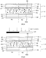
- the display panel of the present embodiment includes a plurality of pixels. As illustrated in Fig. 1 , each pixel includes a transmission region 91 and a reflection region 92, and the display panel includes a first polarizer 11, a first base substrate 19, a first alignment layer 13, a liquid crystal layer 5, a second alignment layer 23, a second base substrate 29, and a second polarizer 21 that are disposed in turn (from top to bottom as illustrated in Fig. 1 ).
- a reflection layer 921 is provided between the second alignment layer 23 and the second polarizer 21 in the reflection region 92.
- the reflection layer 921 is disposed between the second base substrate 29 and the second alignment layer 23, to which the embodiment is not limited however.
- the liquid crystal layer 5 in the reflection region 92 includes nematic liquid crystal 51 and a polymer network 52.
- the liquid crystal layer 5 in the transmission region 91 includes a liquid crystal mixture that includes nematic liquid crystal 51 and polymerizable monomers 521 (as illustrated in Fig. 9 ).
- the alignment direction of nematic liquid crystal 51 in the reflection region 92 is different from the alignment direction of the first alignment layer 13, and the alignment direction of nematic liquid crystal 51 in the transmission region 91 is the same as the alignment direction of the first alignment layer 13.
- the display panel of the present embodiment includes a first substrate 1, a second substrate 2 and a liquid crystal layer 5 sandwiched between the two substrates.
- the first substrate 1 includes a first base substrate 19, and a first polarizer 11 and a first alignment layer 13 that are disposed on the first base substrate 19, and the second substrate 2 includes a second base substrate 29, and a second polarizer 21, a second alignment layer 23 and a reflection layer 921 that are disposed on the second base substrate 29.
- a polymer network 52 is formed in the liquid crystal layer 5 of the reflection region 92.
- the polymer network 52 is formed as follows. After adding the liquid crystal mixture into the liquid crystal layer 5, the polymerizable monomers 521 in the liquid crystal mixture in the liquid crystal layer 5 corresponding to the reflection region 92 are polymerized.
- the polymer network 52 can function to assist alignment of the nematic liquid crystal 51 in the reflection region 92, such that the alignment direction of nematic liquid crystal 51 in the reflection region 92 is different from that of the first alignment layer (such as the direction of friction).
- the alignment direction of nematic liquid crystal 51 in the transmission region 91 is the same as that of the first alignment layer. That is, in case that the alignment directions of the first alignment layers in both the reflection region 92 and the transmission region 91 are the same, the alignment directions of nematic liquid crystal 51 in these two regions are different from each other.
- the nematic liquid crystal 51 is aligned depending on the alignment layer (the first and second alignment layers will be collectively referred to as "alignment layer” hereinbelow because both of them influence the alignment direction of nematic liquid crystal), therefore the polymerizable monomers 521 in this region may not be polymerized but remain in the monomer state. That is, the liquid crystal layer 5 in the transmission region 91 may directly contain the liquid crystal mixture. However, as illustrated in Figs. 1 and 2 , in order to avoid unexpected reactions of the polymerizable monomers 521, it is also possible to allow polymerizable monomers 521 in the transmission region 91 to be polymerized into the polymer network 52 as well.
- the liquid crystal layer 5 in the transmission region 91 may contain the polymer network 52 and the nematic liquid crystal 51.
- the direction of the polymer network 52 in the transmission region 91 is the same as the alignment direction of the alignment layer, and therefore does not change the alignment direction of the nematic liquid crystal 51 in the transmission region 91.
- the polymerizable monomer 521 may have the following structure: the polymerizable monomer 521 has a linear aliphatic chain having ester end group at its molecule end.
- the polymerizable monomer 521 has a phenylene or a biphenylene at the middle of its molecule and at least one methylene, and the phenylene or the biphenylene may be replaced by one or more of alkyl or halogen groups.
- the polymerizable monomer 521 includes at least one phenylene or biphenylene and a (methyl) acrylate end group connected with it via a bivalent alkylidene group, wherein the phenylene or biphenylene has one or more alkyl or halogen substituting groups.
- the degree of functionality of the polymerizable monomers 521 may be greater than 1 for example.
- the exemplary structure of the polymerizable monomer 521 may be expressed in the following formula (I) for example:
- known products that can be used along with the nematic liquid crystal may be adopted as the polymerizable monomers 521.
- commercially available RM257 monomer may be used which has rod-like structure similar to the nematic liquid crystal and therefore may be dissolved well in the nematic liquid crystal, and function to assist alignment of the nematic liquid crystal after polymerization.
- known substance can be used as the polymerizable monomers 521, their specific structures will not be described in detail herein.
- CB5 is used as the nematic liquid crystal 51
- RM257 is used as the polymerizable monomer 521.
- the weight percentage of the polymerizable monomers 521 in the liquid crystal mixture is from 0.01wt% to 15 wt% .
- the above content of the polymerizable monomers 521 may form the polymer network 52 that can function to provide sufficient alignment effect, and will not impose obvious influence on the performance of the nematic liquid crystal 51.
- the polymerizable monomers 521 may be photo polymerizable monomers, and the polymer network 52 is formed by light polymerization of the polymerizable monomers 521 in the liquid crystal mixture.
- the liquid crystal mixture may also contain photoinitiator with a weight percentage from 0.001 wt% to 2 wt% in the liquid crystal mixture.
- the photo polymerizable monomers that may be polymerized under photo illumination such as ultraviolet light irradiation may be used as the polymerizable monomers 521. Because light may be simply blocked, it is possible to easily polymerize polymerizable monomers 521 in various regions respectively. While photo polymerizable monomers are used, it is also possible to add photoinitiator into the liquid crystal mixture to initiate polymerization reaction.
- orientations of polarizer and alignment layers satisfy the following conditions.
- the polarization transmission directions of the first and second polarizers 11 and 21 are perpendicular to each other; orientations (such as rubbing directions) of the first and second alignment layers 13 and 23 are parallel or anti-parallel to each other; and the orientation of the first alignment layer 13 and the polarization direction of the first polarizer 11 are perpendicular to each other.
- the liquid crystal layer 5 in the reflection region 92 can deflect the polarization direction of the linearly polarized light incident in the direction of the first substrate 19 and reflected by the reflection layer 921 by 90 degree.
- the liquid crystal layer 5 in the reflection region 92 can rotate, by 90 degree, the polarization direction of the linearly polarized light that is incident and then reflected, thereby allowing the first polarizer 11 to completely block it to achieve a good dark state effect.
- the liquid crystal layer 5 can generate a phase difference of (2k ⁇ +3 ⁇ /2) for the transmitted visible light, or it may be that the liquid crystal layer 5 can function as a 3/4 wave plate.
- k is 0, and the thickness d of the liquid crystal layer 5 is from 1 ⁇ m to 10 ⁇ m.
- the liquid crystal layer 5 is exactly a 3/4 wave plate only for light of the wavelength ⁇ .
- the phase difference it generates is not (2k ⁇ +3 ⁇ /2); the larger the thickness of liquid crystal layer 5 is, the larger the difference between them is. Therefore, here, by setting k to 0, phase differences of light of other wavelengths are made minimal.
- visible wavelength is generally from 400 nm to 760 nm (for example, ⁇ may be from 530 nm to 580 nm), while the specific birefringence of conventional nematic liquid crystal is about 0.1. Therefore, it is possible to set the thickness d of the liquid crystal layer 5 to from 1 ⁇ m to 10 ⁇ m.
- the equivalent optical axis of the liquid crystal layer 5 of the reflection region 92 forms a 45 degree angle with the polarization transmission direction of the first polarizer 11.
- the alignment direction of the nematic liquid crystal 51 in the reflection region 92 is determined by the polymer network 52 and the alignment layers together, the alignment directions of the nematic liquid crystal 51 at different locations in the thickness direction in the reflection region 92 are different; the closer to the alignment layer the nematic liquid crystal 51 is, the more influence of the alignment layer it experiences, thereby the more approaching the orientation of the alignment layers. On the contrary, nematic liquid crystal 51 farther away from the alignment layer deviates from the orientation of the alignment layer more. Therefore, incapability of accurately pointing out what is the alignment direction of nematic liquid crystal 51 in the reflection region 92 means incapability of pointing out the direction of optical axis of the liquid crystal layer 5 in the reflection region 92.
- the direction of optical axis of the liquid crystal layer 5, namely the direction of optical axis of the nematic liquid crystal 51, is the direction of long axis of the nematic liquid crystal, namely the alignment direction of the nematic liquid crystal.
- the overall function of the liquid crystal layer 5 in the reflection region 92 should be "equivalent to" a liquid crystal layer forming a 45 degree angle with the polarization transmission direction of the first polarizer 11. Therefore, it is that its "equivalent optical axis" forms a 45 degree angle with the polarization transmission direction of the first polarizer 11.
- the equivalent optical axis of the liquid crystal layer 5 in the reflection region 92 satisfies the above conditions, it is just possible to rotate the polarization direction of the incident and reflected linearly polarized light by 90 degrees, thereby achieving a good display effect in the dark state.
- the direction of optical axis of the liquid crystal layer 5 (namely the alignment direction of the nematic liquid crystal 51) is parallel to the orientation of the alignment layers, and light incident from the backlight becomes linearly polarized light with the polarization direction parallel to the optical axis of the liquid crystal layer 5 after passing the second polarizer 21. Therefore, the polarization direction of the light does not change after passing the liquid crystal layer 5, namely the 3/4 wave plate, and it will be completely blocked by the first polarizer 11, thereby achieving a good dark state.
- the reflected light becomes linearly polarized light with the polarization direction forming a 45 degree angle with the "equivalent optical axis" of the liquid crystal layer 5 after passing the first polarizer 11, and becomes circularly polarized light with a certain rotation direction after passing the liquid crystal layer 5 (namely the 3/4 wave plate). While the rotation direction is reversed after the circularly polarized light is reflected by the reflection layer 921; then the light passes the liquid crystal layer 5 (3/4 wave plate) again and becomes linearly polarized light with the polarization direction perpendicular to that of the incident light, and thereby is completely blocked by the first polarizer 11, which also achieves a good dark state.
- the display panel of the present embodiment can guarantee that both regions have good dark state display effects and improve the contrast without adding an in-cell retarder.
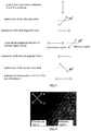
- the transmission region 91 and the reflection region 92 have sharp boundary therebetween and there is substantially no transition (as illustrated in Figs. 4 and 5 ).
- both the transmission region 91 and the reflection region 92 have wide viewing angles (because they may be of the IPS or ADS mode).
- the measured TV curve (the display curve of the transmission region 91) and the measured RV curve (the display curve of the reflection region 92) matches each other well.
- the display panel of the present embodiment further includes: a first half-wave plate 12 and a second half-wave plate 22.
- the first half-wave plate is disposed between the first alignment layer 13 and the first polarizer 11 in which the optical axis of the first half-wave plate 12 is parallel to the equivalent optical axis of the liquid crystal layer 5 in the reflection region 92 in case of no electric field.
- the second half-wave plate is disposed between the second alignment layer 23 and the second polarizer 21 which is farther from the liquid crystal layer 5 than the reflection layer 912 and has an optical axis perpendicular to that of the first half-wave plate 12.
- the first half-wave plate 12 is disposed between the first base substrate 19 and the first polarizer 11
- the second half-wave plate 22 is disposed between the second base substrate 29 and the second polarizer 21, to which the embodiment is however not limited.
- the thickness of the liquid crystal layer 5 can only be set for a specific wavelength, light of other wavelengths in the dark state will experience leakage. Especially for a 3/4 wave plate, it suffers from severer leakage at other wavelengths than a 1/4 wave plate. Therefore, as illustrated in Fig. 1 , it is possible to add a half-wave plate between either of the two substrates and the polarizer to reduce leakage of other wavelengths. Among them, the equivalent optical axis of the liquid crystal layer 5 in the reflection region 92 is parallel to that of the first half-wave plate 12, such that a maximum reflectance can be obtained.
- the two half-wave plates generate a total phase difference of 2k ⁇ , which therefore can not influence the normal display. Because the approach of increasing the bandwidth of a 3/4 wave plate (namely its adaptive wavelength range) by a half-wave plate is known, it will not be described in detail herein.
- the display panel of the present embodiment further includes a first electrode 81 and a second electrode 82 disposed on one base substrate, one of the first electrode 81 and the second electrode 82 is a pixel electrode and the other is a common electrode.
- both the pixel electrode and the common electrode may be disposed in one substrate.
- the electrodes are both disposed in the first substrate 1 (namely the first substrate 1 functioning as the array substrate) will be described.
- the first electrode 81 is a plate electrode
- the second electrode 82 comprises a plurality of strip electrodes
- an insulating layer 83 is disposed between the first electrode 81 and the second electrode 82, and the first electrode 81 is farther away from the liquid crystal layer 5 than the second electrode 82.
- the display panel of the present embodiment may be one of the advanced super dimension switch (ADS) mode, and therefore includes plate electrodes and strip electrodes.
- ADS advanced super dimension switch
- plate electrodes are common electrodes
- strip electrodes are pixel electrodes
- strip electrodes are common electrodes and plate electrodes are pixel electrodes.
- the first electrode 81 and the second electrode 82 both comprise a plurality of strip electrodes that are arranged alternatively.
- the display panel of the present embodiment may also be one of in plane switching (IPS) mode in which alternative strip electrodes are disposed.
- IPS in plane switching
- the each of the above-mentioned strip electrodes (including strip electrodes in the above-mentioned two modes) has a width from 1 ⁇ m to 10 ⁇ m; and the distance between adjacent two of the plurality of strip electrodes is from 1 ⁇ m to 10 ⁇ m.
- the nematic liquid crystal 51 may be liquid crystal of negative dielectric anisotropy. This is because such liquid crystal has a transverse axis perpendicular to the direction of the electric field, and therefore its rotation is mainly in the direction parallel to the substrate plane and more smooth. Of course, it is also feasible to adopt liquid crystal of positive dielectric anisotropy.
- Figs. 4 and 5 show a picture of the boundary between the reflection region 92 and the transmission region 91 of the display panel according to the present embodiment.
- directions of polymer networks 52 in the reflection region 92 and the transmission region 91 are obviously different and boundary between the two regions are remarkably clear. This indicates that the two regions of the display panel of the present embodiment have very obvious and sharp boundary therebetween.
- the display panel of the present embodiment may further include other known structures.
- the display panel of the present embodiment may further include a color filter film (not shown) for color display.
- the color filter film may be disposed on a substrate different from the electrodes (namely a separate color filter substrate), or on the same substrate as the electrodes (namely the COA mode).
- a protection layer (not shown) may be covered on the reflection layer 921.
- the present embodiment provides a manufacturing method of the above-mentioned display panel, including: adding a liquid crystal mixture between the first alignment layer 13 and the second alignment layer 23 and applying an electric field to the liquid crystal mixture, and then allowing only the polymerizable monomers 521 in the liquid crystal mixture in the reflection region 92 to be polymerized into a polymer network 52.
- the above-mentioned liquid crystal mixture is first provided between the two substrates. Then an electric field is applied to deflect the nematic liquid crystal 51 and separately allow polymerizable monomers 521 in the reflection region 92 to be polymerized into a polymer network 52. At the same time, polymerizable monomers 521 in the transmission region 91 do not react such that nematic liquid crystal 51 in the reflection region 92 is aligned into a direction different from the orientation of the alignment layers.
- the method of the present embodiment may include the following steps.
- a liquid crystal mixture is provided between the first substrate 1 and the second substrate 2.
- the liquid crystal mixture includes nematic liquid crystal 51 and polymerizable monomers 521, and may further include photoinitiator as desired.
- a voltage difference is applied between the common electrode and the pixel electrode of each pixel, thereby generating an electric field (such as an electric field parallel to the substrate) in the liquid crystal mixture to drive the nematic liquid crystal 51 in the liquid crystal mixture (including nematic liquid crystal 51 in the transmission region 91 and the reflection region 92) to rotate to a direction different from the orientation of the alignment layers.
- an electric field such as an electric field parallel to the substrate
- the specific strength of electric field is related to many factors such as the dielectric constant, viscosity of the nematic liquid crystal 51, and the anchoring capability of the alignment layers, etc.
- the strength of electric field is generally set to be from 0.5 V/ ⁇ m to 5 V/ ⁇ m.
- a mask for masking transmission regions 91 is disposed on one side of the display panel and light is irradiated to the display panel from one side of the mask, which side is away from the display panel, such that polymerizable monomers 521 in the liquid crystal mixture in the reflection regions 92 are polymerized into the polymer network 52.
- the mask is used to mask the transmission regions 91 while only reflection regions 92 are exposed.
- the display panel is illuminated with light via the mask such that only reflection regions 92 are illuminated and polymerizable monomers 521 in the reflection regions 92 are separated from the liquid crystal mixture and polymerized along intermolecular gaps in the nematic liquid crystal 51 to form the polymer network 52.
- the polymer network 52 duplicates the morphology of liquid crystal at this time to align the nematic liquid crystal 51 in the reflection region 92 into a particular direction different from the orientation of the alignment layers, such that for example the equivalent optical axis of the liquid crystal layer 51 in the reflection region 92 forms a 45 degree angle with the polarization transmission direction of the first polarizer 11.
- the light illumination conditions may be adjusted as desired. Generally, ultraviolet light with an intensity from 0.1 mw/cm 2 to 20 mw/cm 2 can be used to illuminate for 5 ⁇ 60 minutes.
- thermo polymerization it is also feasible to initiate the reaction of polymerizable monomers 521 by other means such as thermal polymerization.
- thermal polymerization it is possible to dispose a plurality of heating blocks that only contact reflection regions 92 for heating.
- thermal polymerization it is difficult for thermal polymerization to guarantee that heat is only conducted to reflection regions 92 but not diffused to transmission regions 91. Therefore, the above-mentioned light polymerization is preferable.
- the nematic liquid crystal 51 in the reflection region 92 is still oriented by the polymer network, while the nematic liquid crystal 51 in the transmission region 91 automatically restores to the state that is the same as the orientation of the alignment layers.
- this step is not necessary. However, in order to prevent remaining polymerizable monomers 521 therein from experiencing unwanted reaction, this step is preferably conducted.
- the above manufacturing method is only a specific example of the present disclosure rather than a limitation to the present disclosure.
- Those skilled in the art may conduct many variations thereto.
- a manufacturing method includes the step of polymerizing polymerizable monomers 521 in the reflection region 92 separately in case of applying electric field, it falls within the scope of the present disclosure.
Landscapes
- Physics & Mathematics (AREA)
- Nonlinear Science (AREA)
- Chemical & Material Sciences (AREA)
- Mathematical Physics (AREA)
- Crystallography & Structural Chemistry (AREA)
- General Physics & Mathematics (AREA)
- Optics & Photonics (AREA)
- Spectroscopy & Molecular Physics (AREA)
- Dispersion Chemistry (AREA)
- Liquid Crystal (AREA)
- Geometry (AREA)
Applications Claiming Priority (2)
| Application Number | Priority Date | Filing Date | Title |
|---|---|---|---|
| CN201510671657.5A CN105223725A (zh) | 2015-10-13 | 2015-10-13 | 显示面板及其制备方法 |
| PCT/CN2016/087455 WO2017063379A1 (zh) | 2015-10-13 | 2016-06-28 | 显示面板及其制备方法 |
Publications (3)
| Publication Number | Publication Date |
|---|---|
| EP3364237A1 true EP3364237A1 (de) | 2018-08-22 |
| EP3364237A4 EP3364237A4 (de) | 2019-05-22 |
| EP3364237B1 EP3364237B1 (de) | 2020-04-29 |
Family
ID=54992771
Family Applications (1)
| Application Number | Title | Priority Date | Filing Date |
|---|---|---|---|
| EP16834013.1A Active EP3364237B1 (de) | 2015-10-13 | 2016-06-28 | Flüssigkristallanzeigetafel und herstellungsverfahren dafür |
Country Status (4)
| Country | Link |
|---|---|
| US (1) | US10705368B2 (de) |
| EP (1) | EP3364237B1 (de) |
| CN (1) | CN105223725A (de) |
| WO (1) | WO2017063379A1 (de) |
Families Citing this family (10)
| Publication number | Priority date | Publication date | Assignee | Title |
|---|---|---|---|---|
| CN105223725A (zh) | 2015-10-13 | 2016-01-06 | 京东方科技集团股份有限公司 | 显示面板及其制备方法 |
| CN107229157A (zh) * | 2016-03-25 | 2017-10-03 | 京东方科技集团股份有限公司 | 透明显示装置及其制备方法 |
| CN107632727B (zh) | 2016-07-18 | 2024-04-12 | 京东方科技集团股份有限公司 | 触摸显示屏及其制备方法、显示装置和驱动方法 |
| CN107340625A (zh) * | 2017-09-01 | 2017-11-10 | 东莞通华液晶有限公司 | 一种聚合物网络液晶显示结构及其制备方法 |
| CN108089363B (zh) | 2017-12-13 | 2020-11-20 | 合肥京东方光电科技有限公司 | 半透半反式阵列基板、其驱动和制备方法及显示面板 |
| CN109143623B (zh) * | 2018-08-27 | 2021-08-10 | 华南师范大学 | 一种红外反射器件及其制备方法 |
| CN113272726B (zh) * | 2019-10-24 | 2022-08-23 | 京东方科技集团股份有限公司 | 显示面板、显示装置及显示面板制造方法 |
| CN112198702A (zh) * | 2020-10-15 | 2021-01-08 | 深圳市华星光电半导体显示技术有限公司 | 显示面板及显示模组 |
| CN112346267B (zh) * | 2020-11-10 | 2022-10-25 | 嘉盛应用材料(河南)有限公司 | 一种显示视角可转换的显示器件及其制备方法 |
| WO2022125627A1 (en) * | 2020-12-08 | 2022-06-16 | Kent State University | Patterned waveguide liquid crystal display |
Family Cites Families (16)
| Publication number | Priority date | Publication date | Assignee | Title |
|---|---|---|---|---|
| CN100543522C (zh) * | 2003-12-12 | 2009-09-23 | 鸿富锦精密工业(深圳)有限公司 | 边缘电场开关型液晶显示装置 |
| CN100376932C (zh) | 2003-12-12 | 2008-03-26 | 鸿富锦精密工业(深圳)有限公司 | 液晶显示装置 |
| TW200537174A (en) | 2004-05-14 | 2005-11-16 | Innolux Display Corp | A transflecitive liquid crystal display apparatus |
| JP4580188B2 (ja) * | 2004-05-27 | 2010-11-10 | 富士通株式会社 | 液晶表示装置及びその製造方法 |
| US8199286B2 (en) * | 2004-07-29 | 2012-06-12 | Kent State University | Polymer stabilized electrically controlled birefringence transflective LCD |
| KR101122235B1 (ko) * | 2005-04-22 | 2012-03-19 | 삼성전자주식회사 | 반투과형 액정 표시 장치 및 그 제조 방법 |
| JP5278720B2 (ja) * | 2006-03-27 | 2013-09-04 | Nltテクノロジー株式会社 | 液晶パネル、液晶表示装置及び端末装置 |
| CN100487535C (zh) * | 2006-08-01 | 2009-05-13 | 友达光电股份有限公司 | 半穿透半反射式液晶显示面板 |
| JP2008102471A (ja) * | 2006-09-21 | 2008-05-01 | Nitto Denko Corp | 液晶パネル、及び液晶表示装置 |
| CN101978025B (zh) * | 2008-03-25 | 2014-09-10 | 默克专利股份有限公司 | 液晶显示器 |
| CN102629034B (zh) * | 2011-07-21 | 2014-11-12 | 京东方科技集团股份有限公司 | 半透射半反射液晶显示器及其制作方法 |
| CN102944958B (zh) | 2012-11-15 | 2015-03-11 | 京东方科技集团股份有限公司 | 一种半透半反液晶显示装置 |
| CN103176307B (zh) | 2013-03-26 | 2015-07-22 | 京东方科技集团股份有限公司 | 半透半反液晶显示面板以及液晶显示装置 |
| CN103207474B (zh) | 2013-03-28 | 2015-05-27 | 京东方科技集团股份有限公司 | 半透半反式液晶显示面板及应用其的显示器 |
| CN103293759A (zh) | 2013-06-27 | 2013-09-11 | 京东方科技集团股份有限公司 | 半透半反显示面板及其制备方法、显示装置 |
| CN105223725A (zh) | 2015-10-13 | 2016-01-06 | 京东方科技集团股份有限公司 | 显示面板及其制备方法 |
-
2015
- 2015-10-13 CN CN201510671657.5A patent/CN105223725A/zh active Pending
-
2016
- 2016-06-28 EP EP16834013.1A patent/EP3364237B1/de active Active
- 2016-06-28 US US15/503,639 patent/US10705368B2/en active Active
- 2016-06-28 WO PCT/CN2016/087455 patent/WO2017063379A1/zh not_active Ceased
Also Published As
| Publication number | Publication date |
|---|---|
| US20170269401A1 (en) | 2017-09-21 |
| US10705368B2 (en) | 2020-07-07 |
| CN105223725A (zh) | 2016-01-06 |
| EP3364237B1 (de) | 2020-04-29 |
| EP3364237A4 (de) | 2019-05-22 |
| WO2017063379A1 (zh) | 2017-04-20 |
Similar Documents
| Publication | Publication Date | Title |
|---|---|---|
| EP3364237B1 (de) | Flüssigkristallanzeigetafel und herstellungsverfahren dafür | |
| KR101198185B1 (ko) | 액정표시장치 및 그 제조방법 | |
| KR100732325B1 (ko) | 수직 배향 액정 필름을 포함하는 위상차 필름 및 그제조방법 | |
| US9250468B2 (en) | Display panel and display unit | |
| US20130169906A1 (en) | Liquid crystal display device | |
| US11262612B2 (en) | Transparent display panel and transparent display device | |
| US8199286B2 (en) | Polymer stabilized electrically controlled birefringence transflective LCD | |
| US20050206809A1 (en) | Method for aligning polymer network liquid crystal | |
| KR101474668B1 (ko) | 투명 디스플레이 | |
| KR20060089132A (ko) | 액정 표시 장치 및 전자 기기 | |
| US20160011460A1 (en) | Transflective liquid crystal display (lcd) panel, display device and array substrate | |
| JPH08278488A (ja) | 液晶表示素子およびその製造方法 | |
| US8570460B2 (en) | Electronically-controllable polarization independent liquid crystal optical medium and devices using same | |
| KR101809987B1 (ko) | 액정 표시 소자 및 그의 제조 방법 | |
| US11886094B2 (en) | Optical element, varifocal element and head mounted display | |
| WO2017208914A1 (ja) | 液晶パネル、スイッチャブル・ミラーパネル及びスイッチャブル・ミラーディスプレイ | |
| KR20130064692A (ko) | 전기-광 위상 변조기 | |
| WO2009081629A1 (ja) | 液晶表示装置及び表示装置用基板 | |
| JP2000162581A (ja) | 反射型液晶表示装置とその製造方法 | |
| CN102998840A (zh) | 显示面板以及具有该显示面板的显示装置 | |
| EP2873712A1 (de) | Polymerstabilisierte, elektrisch unterdrückte, spiralförmige ferroelektrische Flüssigkristallzelle | |
| CN202600308U (zh) | 一种液晶面板以及显示装置 | |
| CN202677027U (zh) | 一种液晶面板以及显示装置 | |
| JP2010224012A (ja) | マルチドメイン化垂直配向型液晶パネル及びこれを具備する液晶表示装置 | |
| US20230185146A1 (en) | Privacy film and display device |
Legal Events
| Date | Code | Title | Description |
|---|---|---|---|
| STAA | Information on the status of an ep patent application or granted ep patent |
Free format text: STATUS: UNKNOWN |
|
| STAA | Information on the status of an ep patent application or granted ep patent |
Free format text: STATUS: THE INTERNATIONAL PUBLICATION HAS BEEN MADE |
|
| PUAI | Public reference made under article 153(3) epc to a published international application that has entered the european phase |
Free format text: ORIGINAL CODE: 0009012 |
|
| STAA | Information on the status of an ep patent application or granted ep patent |
Free format text: STATUS: REQUEST FOR EXAMINATION WAS MADE |
|
| 17P | Request for examination filed |
Effective date: 20170213 |
|
| AK | Designated contracting states |
Kind code of ref document: A1 Designated state(s): AL AT BE BG CH CY CZ DE DK EE ES FI FR GB GR HR HU IE IS IT LI LT LU LV MC MK MT NL NO PL PT RO RS SE SI SK SM TR |
|
| AX | Request for extension of the european patent |
Extension state: BA ME |
|
| DAV | Request for validation of the european patent (deleted) | ||
| DAX | Request for extension of the european patent (deleted) | ||
| A4 | Supplementary search report drawn up and despatched |
Effective date: 20190423 |
|
| RIC1 | Information provided on ipc code assigned before grant |
Ipc: G02F 1/1335 20060101AFI20190415BHEP Ipc: G02F 1/1333 20060101ALI20190415BHEP |
|
| GRAP | Despatch of communication of intention to grant a patent |
Free format text: ORIGINAL CODE: EPIDOSNIGR1 |
|
| STAA | Information on the status of an ep patent application or granted ep patent |
Free format text: STATUS: GRANT OF PATENT IS INTENDED |
|
| INTG | Intention to grant announced |
Effective date: 20191211 |
|
| GRAS | Grant fee paid |
Free format text: ORIGINAL CODE: EPIDOSNIGR3 |
|
| GRAA | (expected) grant |
Free format text: ORIGINAL CODE: 0009210 |
|
| STAA | Information on the status of an ep patent application or granted ep patent |
Free format text: STATUS: THE PATENT HAS BEEN GRANTED |
|
| AK | Designated contracting states |
Kind code of ref document: B1 Designated state(s): AL AT BE BG CH CY CZ DE DK EE ES FI FR GB GR HR HU IE IS IT LI LT LU LV MC MK MT NL NO PL PT RO RS SE SI SK SM TR |
|
| REG | Reference to a national code |
Ref country code: GB Ref legal event code: FG4D |
|
| REG | Reference to a national code |
Ref country code: CH Ref legal event code: EP |
|
| REG | Reference to a national code |
Ref country code: AT Ref legal event code: REF Ref document number: 1264198 Country of ref document: AT Kind code of ref document: T Effective date: 20200515 |
|
| REG | Reference to a national code |
Ref country code: DE Ref legal event code: R096 Ref document number: 602016035328 Country of ref document: DE |
|
| REG | Reference to a national code |
Ref country code: IE Ref legal event code: FG4D |
|
| REG | Reference to a national code |
Ref country code: NL Ref legal event code: MP Effective date: 20200429 |
|
| REG | Reference to a national code |
Ref country code: LT Ref legal event code: MG4D |
|
| PG25 | Lapsed in a contracting state [announced via postgrant information from national office to epo] |
Ref country code: SE Free format text: LAPSE BECAUSE OF FAILURE TO SUBMIT A TRANSLATION OF THE DESCRIPTION OR TO PAY THE FEE WITHIN THE PRESCRIBED TIME-LIMIT Effective date: 20200429 Ref country code: NO Free format text: LAPSE BECAUSE OF FAILURE TO SUBMIT A TRANSLATION OF THE DESCRIPTION OR TO PAY THE FEE WITHIN THE PRESCRIBED TIME-LIMIT Effective date: 20200729 Ref country code: PT Free format text: LAPSE BECAUSE OF FAILURE TO SUBMIT A TRANSLATION OF THE DESCRIPTION OR TO PAY THE FEE WITHIN THE PRESCRIBED TIME-LIMIT Effective date: 20200831 Ref country code: FI Free format text: LAPSE BECAUSE OF FAILURE TO SUBMIT A TRANSLATION OF THE DESCRIPTION OR TO PAY THE FEE WITHIN THE PRESCRIBED TIME-LIMIT Effective date: 20200429 Ref country code: IS Free format text: LAPSE BECAUSE OF FAILURE TO SUBMIT A TRANSLATION OF THE DESCRIPTION OR TO PAY THE FEE WITHIN THE PRESCRIBED TIME-LIMIT Effective date: 20200829 Ref country code: GR Free format text: LAPSE BECAUSE OF FAILURE TO SUBMIT A TRANSLATION OF THE DESCRIPTION OR TO PAY THE FEE WITHIN THE PRESCRIBED TIME-LIMIT Effective date: 20200730 Ref country code: LT Free format text: LAPSE BECAUSE OF FAILURE TO SUBMIT A TRANSLATION OF THE DESCRIPTION OR TO PAY THE FEE WITHIN THE PRESCRIBED TIME-LIMIT Effective date: 20200429 |
|
| REG | Reference to a national code |
Ref country code: AT Ref legal event code: MK05 Ref document number: 1264198 Country of ref document: AT Kind code of ref document: T Effective date: 20200429 |
|
| PG25 | Lapsed in a contracting state [announced via postgrant information from national office to epo] |
Ref country code: LV Free format text: LAPSE BECAUSE OF FAILURE TO SUBMIT A TRANSLATION OF THE DESCRIPTION OR TO PAY THE FEE WITHIN THE PRESCRIBED TIME-LIMIT Effective date: 20200429 Ref country code: HR Free format text: LAPSE BECAUSE OF FAILURE TO SUBMIT A TRANSLATION OF THE DESCRIPTION OR TO PAY THE FEE WITHIN THE PRESCRIBED TIME-LIMIT Effective date: 20200429 Ref country code: RS Free format text: LAPSE BECAUSE OF FAILURE TO SUBMIT A TRANSLATION OF THE DESCRIPTION OR TO PAY THE FEE WITHIN THE PRESCRIBED TIME-LIMIT Effective date: 20200429 Ref country code: BG Free format text: LAPSE BECAUSE OF FAILURE TO SUBMIT A TRANSLATION OF THE DESCRIPTION OR TO PAY THE FEE WITHIN THE PRESCRIBED TIME-LIMIT Effective date: 20200729 |
|
| PG25 | Lapsed in a contracting state [announced via postgrant information from national office to epo] |
Ref country code: NL Free format text: LAPSE BECAUSE OF FAILURE TO SUBMIT A TRANSLATION OF THE DESCRIPTION OR TO PAY THE FEE WITHIN THE PRESCRIBED TIME-LIMIT Effective date: 20200429 Ref country code: AL Free format text: LAPSE BECAUSE OF FAILURE TO SUBMIT A TRANSLATION OF THE DESCRIPTION OR TO PAY THE FEE WITHIN THE PRESCRIBED TIME-LIMIT Effective date: 20200429 |
|
| PG25 | Lapsed in a contracting state [announced via postgrant information from national office to epo] |
Ref country code: RO Free format text: LAPSE BECAUSE OF FAILURE TO SUBMIT A TRANSLATION OF THE DESCRIPTION OR TO PAY THE FEE WITHIN THE PRESCRIBED TIME-LIMIT Effective date: 20200429 Ref country code: IT Free format text: LAPSE BECAUSE OF FAILURE TO SUBMIT A TRANSLATION OF THE DESCRIPTION OR TO PAY THE FEE WITHIN THE PRESCRIBED TIME-LIMIT Effective date: 20200429 Ref country code: SM Free format text: LAPSE BECAUSE OF FAILURE TO SUBMIT A TRANSLATION OF THE DESCRIPTION OR TO PAY THE FEE WITHIN THE PRESCRIBED TIME-LIMIT Effective date: 20200429 Ref country code: AT Free format text: LAPSE BECAUSE OF FAILURE TO SUBMIT A TRANSLATION OF THE DESCRIPTION OR TO PAY THE FEE WITHIN THE PRESCRIBED TIME-LIMIT Effective date: 20200429 Ref country code: DK Free format text: LAPSE BECAUSE OF FAILURE TO SUBMIT A TRANSLATION OF THE DESCRIPTION OR TO PAY THE FEE WITHIN THE PRESCRIBED TIME-LIMIT Effective date: 20200429 Ref country code: MC Free format text: LAPSE BECAUSE OF FAILURE TO SUBMIT A TRANSLATION OF THE DESCRIPTION OR TO PAY THE FEE WITHIN THE PRESCRIBED TIME-LIMIT Effective date: 20200429 Ref country code: EE Free format text: LAPSE BECAUSE OF FAILURE TO SUBMIT A TRANSLATION OF THE DESCRIPTION OR TO PAY THE FEE WITHIN THE PRESCRIBED TIME-LIMIT Effective date: 20200429 Ref country code: ES Free format text: LAPSE BECAUSE OF FAILURE TO SUBMIT A TRANSLATION OF THE DESCRIPTION OR TO PAY THE FEE WITHIN THE PRESCRIBED TIME-LIMIT Effective date: 20200429 Ref country code: CZ Free format text: LAPSE BECAUSE OF FAILURE TO SUBMIT A TRANSLATION OF THE DESCRIPTION OR TO PAY THE FEE WITHIN THE PRESCRIBED TIME-LIMIT Effective date: 20200429 |
|
| REG | Reference to a national code |
Ref country code: CH Ref legal event code: PL |
|
| REG | Reference to a national code |
Ref country code: DE Ref legal event code: R097 Ref document number: 602016035328 Country of ref document: DE |
|
| PG25 | Lapsed in a contracting state [announced via postgrant information from national office to epo] |
Ref country code: SK Free format text: LAPSE BECAUSE OF FAILURE TO SUBMIT A TRANSLATION OF THE DESCRIPTION OR TO PAY THE FEE WITHIN THE PRESCRIBED TIME-LIMIT Effective date: 20200429 Ref country code: PL Free format text: LAPSE BECAUSE OF FAILURE TO SUBMIT A TRANSLATION OF THE DESCRIPTION OR TO PAY THE FEE WITHIN THE PRESCRIBED TIME-LIMIT Effective date: 20200429 |
|
| PLBE | No opposition filed within time limit |
Free format text: ORIGINAL CODE: 0009261 |
|
| STAA | Information on the status of an ep patent application or granted ep patent |
Free format text: STATUS: NO OPPOSITION FILED WITHIN TIME LIMIT |
|
| PG25 | Lapsed in a contracting state [announced via postgrant information from national office to epo] |
Ref country code: LU Free format text: LAPSE BECAUSE OF NON-PAYMENT OF DUE FEES Effective date: 20200628 |
|
| 26N | No opposition filed |
Effective date: 20210201 |
|
| REG | Reference to a national code |
Ref country code: BE Ref legal event code: MM Effective date: 20200630 |
|
| PG25 | Lapsed in a contracting state [announced via postgrant information from national office to epo] |
Ref country code: CH Free format text: LAPSE BECAUSE OF NON-PAYMENT OF DUE FEES Effective date: 20200630 Ref country code: LI Free format text: LAPSE BECAUSE OF NON-PAYMENT OF DUE FEES Effective date: 20200630 Ref country code: IE Free format text: LAPSE BECAUSE OF NON-PAYMENT OF DUE FEES Effective date: 20200628 |
|
| PG25 | Lapsed in a contracting state [announced via postgrant information from national office to epo] |
Ref country code: BE Free format text: LAPSE BECAUSE OF NON-PAYMENT OF DUE FEES Effective date: 20200630 Ref country code: SI Free format text: LAPSE BECAUSE OF FAILURE TO SUBMIT A TRANSLATION OF THE DESCRIPTION OR TO PAY THE FEE WITHIN THE PRESCRIBED TIME-LIMIT Effective date: 20200429 |
|
| PG25 | Lapsed in a contracting state [announced via postgrant information from national office to epo] |
Ref country code: TR Free format text: LAPSE BECAUSE OF FAILURE TO SUBMIT A TRANSLATION OF THE DESCRIPTION OR TO PAY THE FEE WITHIN THE PRESCRIBED TIME-LIMIT Effective date: 20200429 Ref country code: MT Free format text: LAPSE BECAUSE OF FAILURE TO SUBMIT A TRANSLATION OF THE DESCRIPTION OR TO PAY THE FEE WITHIN THE PRESCRIBED TIME-LIMIT Effective date: 20200429 Ref country code: CY Free format text: LAPSE BECAUSE OF FAILURE TO SUBMIT A TRANSLATION OF THE DESCRIPTION OR TO PAY THE FEE WITHIN THE PRESCRIBED TIME-LIMIT Effective date: 20200429 |
|
| PG25 | Lapsed in a contracting state [announced via postgrant information from national office to epo] |
Ref country code: MK Free format text: LAPSE BECAUSE OF FAILURE TO SUBMIT A TRANSLATION OF THE DESCRIPTION OR TO PAY THE FEE WITHIN THE PRESCRIBED TIME-LIMIT Effective date: 20200429 |
|
| PGFP | Annual fee paid to national office [announced via postgrant information from national office to epo] |
Ref country code: DE Payment date: 20250618 Year of fee payment: 10 |
|
| PGFP | Annual fee paid to national office [announced via postgrant information from national office to epo] |
Ref country code: GB Payment date: 20250618 Year of fee payment: 10 |
|
| PGFP | Annual fee paid to national office [announced via postgrant information from national office to epo] |
Ref country code: FR Payment date: 20250625 Year of fee payment: 10 |