EP3364604B1 - Brückengleichrichter mit intelligenten bypass-dioden - Google Patents
Brückengleichrichter mit intelligenten bypass-dioden Download PDFInfo
- Publication number
- EP3364604B1 EP3364604B1 EP17198049.3A EP17198049A EP3364604B1 EP 3364604 B1 EP3364604 B1 EP 3364604B1 EP 17198049 A EP17198049 A EP 17198049A EP 3364604 B1 EP3364604 B1 EP 3364604B1
- Authority
- EP
- European Patent Office
- Prior art keywords
- bridge rectifier
- smart bypass
- power
- bypass diode
- examples
- Prior art date
- Legal status (The legal status is an assumption and is not a legal conclusion. Google has not performed a legal analysis and makes no representation as to the accuracy of the status listed.)
- Active
Links
Images


Classifications
-
- H—ELECTRICITY
- H04—ELECTRIC COMMUNICATION TECHNIQUE
- H04L—TRANSMISSION OF DIGITAL INFORMATION, e.g. TELEGRAPHIC COMMUNICATION
- H04L12/00—Data switching networks
- H04L12/02—Details
- H04L12/10—Current supply arrangements
-
- H—ELECTRICITY
- H02—GENERATION; CONVERSION OR DISTRIBUTION OF ELECTRIC POWER
- H02M—APPARATUS FOR CONVERSION BETWEEN AC AND AC, BETWEEN AC AND DC, OR BETWEEN DC AND DC, AND FOR USE WITH MAINS OR SIMILAR POWER SUPPLY SYSTEMS; CONVERSION OF DC OR AC INPUT POWER INTO SURGE OUTPUT POWER; CONTROL OR REGULATION THEREOF
- H02M7/00—Conversion of AC power input into DC power output; Conversion of DC power input into AC power output
- H02M7/02—Conversion of AC power input into DC power output without possibility of reversal
- H02M7/04—Conversion of AC power input into DC power output without possibility of reversal by static converters
- H02M7/06—Conversion of AC power input into DC power output without possibility of reversal by static converters using discharge tubes without control electrode or semiconductor devices without control electrode
-
- H—ELECTRICITY
- H04—ELECTRIC COMMUNICATION TECHNIQUE
- H04L—TRANSMISSION OF DIGITAL INFORMATION, e.g. TELEGRAPHIC COMMUNICATION
- H04L12/00—Data switching networks
- H04L12/28—Data switching networks characterised by path configuration, e.g. LAN [Local Area Networks] or WAN [Wide Area Networks]
- H04L12/40—Bus networks
- H04L12/40006—Architecture of a communication node
- H04L12/40045—Details regarding the feeding of energy to the node from the bus
Definitions
- Networks can include a plurality of access points that can utilize a plurality of Ethernet ports to communicate with other network devices.
- the plurality of Ethernet ports can include ports that support power over Ethernet (PoE).
- PoE can be utilized to transfer electrical current via the Ethernet data cables rather than via power cables. PoE can minimize the quantity of wires connected to a network device.
- US 2007/171690 A1 relates to a circuit having a diode bridge, a sensed circuit element, and a controller.
- the diode bridge includes a plurality of diodes and at least one diode bypass element associated with at least one of the plurality of diodes.
- the controller determines an electrical parameter of the sensed circuit element and generates a control signal to activate the at least one diode bypass element in response to determining the electrical parameter.
- US 2014/084681 A1 relates to a system for sinking maintain power signature (MPS) current to a rectifier bridge from a powered device (PD) controller in a Power over Ethernet (PoE) network.
- the system includes a rectifier bridge configured to electrically connect to Power over Ethernet power sourcing equipment for receiving power from the power sourcing equipment.
- the system also includes a powered device controller operatively connected to the rectifier bridge and configured to control power supplied to a load.
- the load is configured to receive power from the power sourcing equipment and a second power source.
- the powered device controller is configured to source maintain power signature current to the power sourcing equipment using an input of the rectifier bridge when the second power source is furnishing power to the load.
- US 8 674 546 B1 relates to a VoIP switch, which includes a first input Ethernet port configured to receive electrical power from a first power sourcing equipment, and a second input Ethernet port configured to receive electrical power from a second power sourcing equipment.
- the VoIP switch may be configured such that the first input Ethernet port is powered by the first power sourcing equipment concurrently with the second input Ethernet port being powered by the second power sourcing equipment.
- CN 101 594 236 B relates to a method for realizing power over Ethernet (POE), which comprises the steps of: receiving direct current power supplies provided by power supply equipment (PSE) through at least two ports at a PD side of power receiving equipment, performing load balancing processing on a plurality of the direct current power supplies which enter from the at least two ports, and outputting the direct current power supplies which are subjected to load balancing processing to loads.
- PSE power supply equipment
- the system also provides a POE control device and a POE system.
- the direct current power supplies are received through multiple ports at a power receiving equipment side, and a plurality of the direct current power supplies are subjected to load balancing processing, so that the functions of load balancing and redundancy backup of the POE are realized, and the stability of system operation is improved.
- US 9 485 103 B2 relates to a network powered device which includes field effect transistors connected as bridge circuit.
- the bridge circuit includes control circuitry to enable the FETs based on completion of a powered device detection sequence performed by power sourcing equipment coupled to the device via an Ethernet link.
- US 2009/168278 A1 relates to a circuit device which includes a diode bridge having a first power input and a second power input and having a first output terminal and a second output terminal.
- the diode bridge includes a plurality of diodes and a respective plurality of diode bypass elements associated with the plurality of diodes.
- the circuit device further includes a logic circuit to detect a power event at the first and second power inputs and to selectively activate one or more of the respective plurality of diode bypass elements in response to detecting the power event to limit a rectified power supply at the first and second output terminals.
- Smart bypass diode bridge rectifiers can enable a device to utilize a plurality of Ethernet ports for power over Ethernet (PoE).
- the device can be a network device such as an access point.
- 'access point' can, for example, refer to receiving points for any known or convenient wireless access technology which may later become known.
- the term AP is not intended to be limited to IEEE 802.11-based APs.
- APs generally function as an electronic device that is adapted to allow wireless devices to connect to a wired network via various communications standards.
- Utilizing PoE can reduce a quantity of wires to be connected to the device.
- a single Ethernet port utilizing PoE can deliver power and data to the device.
- the device can include a plurality of Ethernet ports that can be utilized to send and receive data.
- a device may utilize a single Ethernet port for PoE.
- power provided by a first power sourcing equipment (PSE) device connected to a first PoE port can deactivate a second PSE device connected to a second PoE port.
- PSE power sourcing equipment
- multiple PoE ports may not be capable of being utilized as a backup PoE ports if one or more PoE ports fail and/or may not be capable of utilizing multiple PoE ports together to provide additional power to the device.
- a smart bypass diode bridge rectifier can comprise a plurality of smart diodes to form a bridge rectifier.
- a 'bridge rectifier' can, for example, refer to a number of diodes (e.g., four diodes, etc.) in a bridge arrangement to achieve full-wave rectification.
- the number of diodes are smart bypass diodes to form a smart bypass diode bridge rectifier.
- a 'smart bypass diode' can, for example, refer to a diode that acts as a MOSFET diode above a threshold voltage and prevents a reverse bias.
- the smart bypass diodes can provide no forward voltage drop.
- P-N junction diodes or Schottky diodes were used to mitigate a reverse bias, but these diodes have a relatively high forward voltage drop (e.g., 0.6 Volt (V) for P-N junction diodes and 0.4 V for Schottky diodes, etc.).
- the smart bypass diode can include a 30 V maximum reverse voltage (VR), a 15 Amp (A) maximum forward current (IF), a relatively low forward voltage drop, and/or relatively less power dissipation and lower leakage current compared to Schottky diodes.
- the smart bypass diode bridge rectifiers can be utilized to prevent a deadlock when a plurality of PoE ports are utilized by a device.
- the device can include a first PoE input connected to a first smart bypass diode bridge rectifier and a second PoE input connected to a second smart bypass diode bridge rectifier.
- the first and second smart bypass diode bridge rectifiers can prevent a deadlock between the first PoE input and the second PoE input by preventing a reverse bias.
- the smart bypass diode bridge rectifiers can reduce power dissipation (e.g., 96.28% reduction) compared to other types of H-bridge rectifiers.
- the smart bypass diode bridge rectifiers can be utilized to achieve hitless failover between the plurality of PoE ports of a device.
- Figure 1 illustrates an example device 100 for smart bypass diode bridge rectifiers, consistent with the present disclosure.
- the device 100 can be a network device such as an access point or controller.
- the device 100 can include a PoE port (e.g., ETH0) that can include a first input 102-1 (e.g., negative input, etc.) and a second input 102-2 (e.g., positive input, etc.).
- a PoE port can be utilized to transfer data and power to the device 100.
- the PoE port can be connected to a smart bypass diode bridge rectifier 104.
- the smart bypass diode bridge rectifier 104 can be a H-bridge rectifier that utilizes a number of smart bypass diodes 106-1, 106-2, 106-3, 106-4.
- the smart bypass diodes 106-1, 106-2, 106-3, 106-4 can include diodes that act as MOSFET diodes above a threshold voltage and prevent a reverse bias.
- the smart bypass diodes 106-1, 106-2, 106-3, 106-4 can provide no forward voltage drop.
- the smart bypass diodes 106-1, 106-2, 106-3, 106-4 can include a 30 V maximum reverse voltage (VR), a 15 Amp (A) maximum forward current (IF), a relatively low forward voltage drop, and/or relatively less power dissipation and lower leakage current compared to Schottky diodes.
- VR maximum reverse voltage
- A 15 Amp
- IF maximum forward current
- a relatively low forward voltage drop and/or relatively less power dissipation and lower leakage current compared to Schottky diodes.
- the PoE port can be connected to power source equipment (PSE) devices that can provide electrical power to the device 100.
- PSE power source equipment
- the PoE port can include a first input 102-1 that can be connected to a negative terminal of a power source and/or a negative terminal of the PSE device.
- the second input 102-2 can be connected to a positive terminal of a power source and/or a negative terminal of the PSE device.
- the first input 102-1 can be connected to a positive terminal and the second input 102-2 can be connected to a negative terminal.
- electrical power can be transferred through the first input 102-1 via a pathway comprising a plurality of points 108-1, 108-2, 108-3, 108-4, 108-5, 108-6 to a powered device (PD).
- a powered device PD
- electrical power from a negative terminal of a PSE device can be received at the input 102-1 and proceed to a first point 108-1, proceed to a second point 108-2, proceed to a third point 108-3, proceed to a smart diode 106-2, proceed to a fourth point 108-4, proceed to a fifth point 108-5, proceed to a sixth point 108-6 and then proceed to a first connection of a powered device 110.
- a second connection of the powered device can be connected to a first connection of a load 112.
- a second connection of the load 112 can be connected to the smart bypass diode bridge rectifier 104 via smart bypass diode 106-3.
- the smart bypass diode bridge rectifier 104 can be utilized to allow for different types of PSE devices to be connected to the device.
- PSE devices can utilize a positive terminal for connecting to the first input 102-1 and a negative terminal for connecting to the second input 102-1.
- the smart bypass diode bridge rectifier 104 can be utilized to avoid deadlock between PSE devices when multiple PoE ports are utilized to provide power to the device 100.
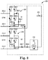
- Figure 2 further illustrates an example device 220 for smart bypass diode bridge rectifiers, consistent with the present disclosure.
- the device 220 can be a network device such as an access point or controller.
- the device 220 can include a first PoE port (e.g., ETH0) and a second PoE port (e.g., ETH1).
- the first PoE port can include a first input 202-1 (e.g., negative input, etc.) and a second input 202-2 (e.g., positive input, etc.).
- the second PoE port can include a first input 214-1 (e.g., negative input) and a second input 214-2 (e.g., positive input).
- the first PoE port and the second PoE port can each be utilized to transfer data and power to the device 220.
- the first PoE port can be connected to a first smart bypass diode bridge rectifier 204.
- the first smart bypass diode bridge rectifier 204 can be a H-bridge rectifier that utilizes a number of smart bypass diodes 206-1, 206-2, 206-3, 206-4.
- the smart bypass diodes 206-1, 206-2, 206-3, 206-4 can include diodes that act as MOSFET diodes above a threshold voltage and prevent a reverse bias.
- the smart bypass diodes 206-1, 206-2, 206-3, 206-4 can provide no forward voltage drop.
- the smart bypass diodes 206-1, 206-2, 206-3, 206-4 can include a 30 V maximum reverse voltage (VR), a 15 Amp (A) maximum forward current (IF), a relatively low forward voltage drop, and/or relatively less power dissipation and lower leakage current compared to Schottky diodes.
- VR maximum reverse voltage
- A 15 Amp
- IF maximum forward current
- a relatively low forward voltage drop and/or relatively less power dissipation and lower leakage current compared to Schottky diodes.
- the first PoE port can be connected to a first power source equipment (PSE) device that can provide electrical power to the device 220.
- the first PoE port can include a first input 202-1 that can be connected to a negative terminal of a power source and/or a negative terminal of the first PSE device.
- the second input 202-2 can be connected to a positive terminal of a power source and/or a positive terminal of the first PSE device.
- the first input 202-1 can be connected to a positive terminal and the second input 202-2 can be connected to a negative terminal.
- the second PoE port can be connected to a second smart bypass diode bridge rectifier 216.
- the second smart bypass diode bridge rectifier 216 can be connected to a parallel bridge rectifier (e.g., smart bypass diode bridge rectifier 204, etc.) connected to a parallel power over Ethernet port (e.g., PoE port (ETH0), PoE input 202-1, PoE input 202-2, etc.).
- the second smart bypass diode bridge rectifier 216 can be a H-bridge rectifier that utilizes a number of smart bypass diodes 218-1, 218-2, 218-3, 218-4.
- the smart bypass diodes 218-1, 218-2, 218-3, 218-4 can include diodes that act as MOSFET diodes above a threshold voltage and prevent a reverse bias.
- the smart bypass diodes 218-1, 218-2, 218-3, 218-4 can provide no forward voltage drop.
- the smart bypass diodes 218-1, 218-2, 218-3, 218-4 can include a 30 V maximum reverse voltage (VR), a 15 Amp (A) maximum forward current (IF), a relatively low forward voltage drop, and/or relatively less power dissipation and lower leakage current compared to Schottky diodes.
- the second PoE port can be connected to a second PSE device that can provide electrical power to the device 220.
- the second PoE port can include a first input 214-1 that can be connected to a negative terminal of a power source and/or a negative terminal of the second PSE device.
- the second input 214-2 can be connected to a positive terminal of a power source and/or a positive terminal of the second PSE device.
- the first input 214-1 can be connected to a positive terminal and the second input 214-2 can be connected to a negative terminal.
- electrical power can be transferred through the first input 202-1 of the first PoE port via a pathway comprising a plurality of points 208-1, 208-2, 208-3, 208-4, 208-5, 208-6 to a powered device (PD).
- PD powered device
- electrical power from a negative terminal of a first PSE device can be received at the input 202-1 and proceed to a first point 208-1, proceed to a second point 208-2, proceed to a third point 208-3, proceed to a smart diode 206-2, proceed to a fourth point 208-4, proceed to a fifth point 208-5, proceed to a sixth point 208-6 and then proceed to a first connection of a powered device 210.
- a second connection of the powered device 210 can be connected to a first connection of a load 212.
- a second connection of the load 212 can be connected to the smart bypass diode bridge rectifier 204 via smart bypass diode 206-3.
- the electrical power transferred through the first input 202-1 can proceed to the second smart bypass diode bridge rectifier 216 via point 208-7, proceed to point 208-8, and then proceed to smart bypass diode 218-2 of the second smart bypass diode bridge rectifier 216.
- the smart bypass diode 218-2 can prevent a reverse bias and thus prevent the electrical power from being transferred through the second smart bypass diode bridge rectifier 216 to the first input 214-1 of the second PoE port.
- the second smart bypass diode bridge rectifier 216 can prevent electrical power from being provided to a second PSE device.
- the second smart bypass diode bridge rectifier 216 can prevent the electrical power such that the second PSE device is not deactivated or remains activated.
- electrical power provided to the first input 214-1 through the second smart bypass diode bridge rectifier 216 can deactivate a second PSE device connected to the second PoE port. In some examples, this deactivation can be known as deadlock between the first PSE device and the second PSE device.
- the first input 202-1 of the first PoE port can be connected between a first smart bypass diode 206-1 and a second smart bypass diode 206-2 of the at least four smart bypass diodes of the first smart bypass diode bridge rectifier 204.
- the second input 202-2 of the first PoE port is connected between a third smart bypass diode 206-3 and a fourth smart bypass diode 206-4 of the at least four smart bypass diodes of the first bridge rectifier 304.
- the first input 214-1 of the second PoE port can be connected between a first smart bypass diode 218-1 and a second smart bypass diode 218-2 of the at least four smart bypass diodes of the second smart bypass diode bridge rectifier 316.
- the second input 214-2 of the second PoE port is connected between a third smart bypass diode 218-3 and a fourth smart bypass diode 218-4 of the at least four smart bypass diodes of the second bridge rectifier 316.
- the smart bypass diode bridge rectifiers 204, 216 can be utilized to prevent a deadlock when a plurality of PoE ports are utilized by a device 220.
- the device 220 can include a first PoE input connected to a first smart bypass diode bridge rectifier 204 and a second PoE input connected to a second smart bypass diode bridge rectifier 216.
- the first smart bypass diode bridge rectifier 204 and second smart bypass diode bridge rectifier 216 can prevent a deadlock between the first PSE device and the second PSE device by preventing a reverse bias.
- the smart bypass diode bridge rectifiers 204, 216 can reduce power dissipation (e.g., 96.28% reduction) compared to other types of H-bridge rectifiers.
- the smart bypass diode bridge rectifiers 204, 216 can be utilized to achieve hitless failover between the plurality of PoE ports of a device 220.
- a device 320 can be a network device such as an access point or controller.
- the device 320 can include a first PoE port (e.g., ETH0) and a second PoE port (e.g., ETH1).
- the first PoE port can include a first input 302-1 (e.g., negative input, etc.) and a second input 302-2 (e.g., positive input, etc.).
- the second PoE port can include a first input 314-1 (e.g., negative input) and a second input 314-2 (e.g., positive input).
- the first PoE port and the second PoE port can each be utilized to transfer data and power to the device 320.
- the first PoE port can be a parallel PoE port to the second PoE port.
- the device 320 can be connected to a device 321.
- the device 321 can be a network switch such as a PoE switch that can utilize PoE to power device 320.
- the device 321 can be connected to device 320 via the first PoE port and the second Poe port.
- the device 321 can include a power source 332.
- the power source can be a power input that is connected to an electrical power grid.
- the power source 332 can be connected to a plurality of power sourcing equipment (PSE) devices 334-1, 334-2.
- PSE devices 334-1, 334-2 can be utilized to convert the electrical power from the power source 332 to be transferred to the device 320 via PoE.
- the PSE devices 334-1, 334-2 can alter a voltage or current of the electrical power provided by the power source 332 based on a specification of the PSE devices 334-1, 334-2 and/or a specification of the powered device 310 of the device 320.
- a first PSE device 334-1 of the device 321 can be connected to a first PoE port of the device 320 that can be connected to a first smart bypass diode bridge rectifier 104.
- the first smart bypass diode bridge rectifier 304 can be a H-bridge rectifier that utilizes a number of smart bypass diodes.
- the smart bypass diodes can include diodes that act as MOSFET diodes above a threshold voltage and prevent a reverse bias. In some examples, the smart bypass diodes can provide no forward voltage drop.
- the smart bypass diodes can include a 30 V maximum reverse voltage (VR), a 15 Amp (A) maximum forward current (IF), a relatively low forward voltage drop, and/or relatively less power dissipation and lower leakage current compared to Schottky diodes.
- the first PoE port can be connected to the first power source equipment (PSE) device 334-1 that can provide electrical power to the device 220.
- the first PoE port can include a first input 302-1 that can be connected to a negative terminal of the power source 332 and/or a negative terminal of the first PSE device 334-1.
- the first input 302-1 can be connected to a switch 336-1.
- the switch 336-1 can be connected to a negative terminal of the power source 332 and a negative terminal of the first PSE device 334-1.
- the switch 336-1 can be activated and/or deactivated via the electrical power provided by the power source 332.
- the second input 302-2 can be connected to a positive terminal of the power source 332 and/or a positive terminal of the first PSE device 334-1.
- the first input 302-1 can be connected to a positive terminal and the second input 302-2 can be connected to a negative terminal.
- the second PoE port can be connected to a second PSE device 334-2 that can provide electrical power to a second smart bypass diode bridge rectifier 316.
- the second smart bypass diode bridge rectifier 316 can be a H-bridge rectifier that utilizes a number of smart bypass diodes.
- the smart bypass diodes can include diodes that act as MOSFET diodes above a threshold voltage and prevent a reverse bias. In some examples, the smart bypass diodes can provide no forward voltage drop.
- the smart bypass diodes can include a 30 V maximum reverse voltage (VR), a 15 Amp (A) maximum forward current (IF), a relatively low forward voltage drop, and/or relatively less power dissipation and lower leakage current compared to Schottky diodes.
- the second PoE port can be connected to the second PSE device 334-2 that can provide electrical power to the device 320.
- the second PoE port can include a first input 314-1 that can be connected to a negative terminal of the power source 332 and/or a negative terminal of the second PSE device 334-2.
- the second input 314-2 can be connected to a positive terminal of the power source 332 and/or a positive terminal of the second PSE device 334-2.
- the first input 314-1 can be connected to a positive terminal and the second input 314-2 can be connected to a negative terminal.
- electrical power can be transferred through the first input 302-1 of the first PoE port via a pathway comprising a plurality of points to a powered device (PD) 310.
- a powered device PD
- electrical power from a negative terminal of the first PSE device 334-1 can be received at the input 302-1 and proceed to a smart diode 306-2 and then proceed to a first connection of a powered device 310.
- a second connection of the powered device 310 can be connected to a first connection of a load 312.
- a second connection of the load 312 can be connected to the first smart bypass diode bridge rectifier 304 via smart bypass diode 306-3.
- the electrical power transferred through the first input 302-1 can proceed to the second smart bypass diode bridge rectifier 316 via intersection 322 and then proceed to a smart bypass diode (e.g., smart bypass diode D6, etc.) of the second smart bypass diode bridge rectifier 316.
- a smart bypass diode e.g., smart bypass diode D6, etc.
- the smart bypass diode can prevent a reverse bias and thus prevent the electrical power from being transferred through the second smart bypass diode bridge rectifier 316 to the first input 314-1 of the second PoE port.
- the second smart bypass diode bridge rectifier 316 can prevent electrical power from being provided to a second PSE device 334-2 of the device 321 via the first input 314 of the second PoE port. In these examples, the second smart bypass diode bridge rectifier 316 can prevent the electrical power such that the second PSE device 334-2 is not deactivated or remains activated. For example, electrical power provided to the first input 314-1 through the second smart bypass diode bridge rectifier 316 can proceed to switch 336-2 and deactivate a second PSE device 334-2 connected to the second PoE port. In some examples, this deactivation can be known as deadlock between the first PSE device 334-1 and the second PSE device 334-2.
- the first input 302-1 can be connected between a first smart bypass diode D1 and a second smart bypass diode D2 of the at least four smart bypass diodes of the first smart bypass diode bridge rectifier 304.
- the second input 302-2 is connected between a third smart bypass diode D3 and a fourth smart bypass diode D4 of the at least four smart bypass diodes of the first bridge rectifier 304.
- the first smart bypass diode bridge rectifier 304 and the second smart bypass diode bridge rectifier 316 accept a coupling from type A power source equipment devices and type B power source equipment devices.
- the first PoE port can be connected to either a type A power source equipment device or a type B power source equipment device.
- a 'type A power source equipment device' can, for example, refer to a PSE device that transmits power on the same wires as data for 10 Megabits per second (Mbit/s) and 100 Mbit/s.
- the type A power source equipment can be similar to phantom power techniques.
- a 'type B power source equipment device' can, for example, refer to a PSE device that utilizes separate data and power conductors for transmitting data on a first wire and transmitting power on a second wire.
- the smart bypass diode bridge rectifiers 304, 316 can be utilized to prevent a deadlock between the first PSE device 334-1 and the second PSE device 334-2 when a plurality of PoE ports are utilized to connect a device 321 to a device 320.
- the device 320 can include a first PoE port connected to a first smart bypass diode bridge rectifier 304 and a second PoE port connected to a second smart bypass diode bridge rectifier 316.
- the first smart bypass diode bridge rectifier 304 and second smart bypass diode bridge rectifier 316 can prevent a deadlock between the first PSE device 334-1 and the second PSE device 334-2 by preventing a reverse bias.
- the smart bypass diode bridge rectifiers 304, 316 can reduce power dissipation (e.g., 96.28% reduction) compared to other types of H-bridge rectifiers.
- the smart bypass diode bridge rectifiers 304, 316 can be utilized to achieve hitless failover between the plurality of PoE ports of a device 320.
Landscapes
- Engineering & Computer Science (AREA)
- Computer Networks & Wireless Communication (AREA)
- Signal Processing (AREA)
- Power Engineering (AREA)
- Rectifiers (AREA)
- Direct Current Feeding And Distribution (AREA)
Claims (7)
- Netzwerkvorrichtung, Folgendes umfassend:einen ersten Eingang (202) für eine Stromversorgung über Ethernet, der mit mehreren ersten intelligenten Bypass-Dioden (206) verbunden ist, die einen ersten Brückengleichrichter (204) ausbilden, wobei der erste Eingang (202) für eine Stromversorgung über Ethernet angeordnet ist, um mit einer ersten Stromquellenausrüstungsvorrichtung verbunden zu werden;einen zweiten Eingang (214) für eine Stromversorgung über Ethernet, der mit mehreren zweiten intelligenten Bypass-Dioden (218) verbunden ist, die einen zweiten Brückengleichrichter (216) ausbilden, der mit dem ersten Brückengleichrichter (204) verbunden ist, wobei der zweite Eingang (214) für eine Stromversorgung über Ethernet angeordnet ist, um mit einer zweiten Stromquellenausrüstungsvorrichtung verbunden zu werden; undeine angetriebene Vorrichtung, die mit dem ersten Brückengleichrichter (204) und dem zweiten Brückengleichrichter (216) verbunden (210) ist, wobei der zweite Brückengleichrichter (216) angeordnet ist, um eine Sperrvorspannung daran zu hindern, Strom an die zweite Stromquellenausrüstungsvorrichtung zu liefern.
- Netzwerkvorrichtung nach Anspruch 1, wobei das Liefern von Strom an die zweite Stromquellenausrüstungsvorrichtung von dem zweiten Brückengleichrichter (216) die zweite Stromquellenausrüstungsvorrichtung deaktiviert.
- Netzwerkvorrichtung nach Anspruch 2, wobei der erste Brückengleichrichter (204) und der zweite Brückengleichrichter (216) eine Kopplung mit Stromquellenausrüstungsvorrichtungen des Typs A und Stromquellenausrüstungsvorrichtungen des Typs B annehmen.
- System, Folgendes umfassend:einen ersten Eingang (302) für eine Stromversorgung über Ethernet, der mit wenigstens vier intelligenten Bypass-Dioden (D1-D4) verbunden ist, die einen ersten Brückengleichrichter (304) ausbilden, wobei der erste Eingang (302) für eine Stromversorgung über Ethernet mit einer ersten Stromquellenausrüstungsvorrichtung (334-1) verbunden ist, die Strom an den den ersten Brückengleichrichter (304) liefert;einen zweiten Eingang (314) für eine Stromversorgung über Ethernet, der mit wenigstens vier intelligenten Bypass-Dioden (D5-D8) verbunden ist, die einen zweiten Brückengleichrichter (316), der mit dem ersten Brückengleichrichter (304) verbunden ist, ausbilden, wobei der zweite Eingang (314) für eine Stromversorgung über Ethernet mit einer zweiten Stromquellenausrüstungsvorrichtung (334-2) verbunden ist, die Strom an den zweiten Brückengleichrichter (316) liefert.eine angetriebene Vorrichtung (310), die mit dem ersten Brückengleichrichter (304) und dem zweiten Brückengleichrichter (316) verbunden ist, wobei der zweite Brückengleichrichter (316) angeordnet ist, um eine Sperrvorspannung daran zu hindern, Strom an die zweite Stromquellenausrüstungsvorrichtung (332-2) zu liefern; undeine Ladung (312), die mit der angetriebenen Vorrichtung (310) und dem ersten Brückengleichrichter (312) verbunden ist.
- System nach Anspruch 4, wobei der erste Eingang (302) für eine Stromversorgung über Ethernet zwischen eine erste intelligente Bypass-Diode und eine zweite intelligente Bypass-Diode der wenigstens vier intelligenten Bypass-Dioden (D1-D4) des ersten Brückengleichrichters (304) geschaltet ist.
- System nach Anspruch 5, wobei der zweite Eingang (314) für eine Stromversorgung über Ethernet zwischen eine dritte intelligente Bypass-Diode und eine vierte intelligente Bypass-Diode der wenigstens vier intelligenten Bypass-Dioden (D5-D8) des zweiten Brückengleichrichters (316) geschaltet ist.
- System nach Anspruch 6, wobei eine fünfte intelligente Bypass-Diode der wenigstens vier intelligenten Bypass-Dioden des zweiten Brückengleichrichters (316) verhindert, dass eine Sperrvorspannung an die zweite Stromquellenausrüstungsvorrichtung (334-2) geliefert wird.
Applications Claiming Priority (1)
| Application Number | Priority Date | Filing Date | Title |
|---|---|---|---|
| US15/437,998 US10790996B2 (en) | 2017-02-21 | 2017-02-21 | Smart bypass diode bridge rectifiers |
Publications (2)
| Publication Number | Publication Date |
|---|---|
| EP3364604A1 EP3364604A1 (de) | 2018-08-22 |
| EP3364604B1 true EP3364604B1 (de) | 2019-06-26 |
Family
ID=60162140
Family Applications (1)
| Application Number | Title | Priority Date | Filing Date |
|---|---|---|---|
| EP17198049.3A Active EP3364604B1 (de) | 2017-02-21 | 2017-10-24 | Brückengleichrichter mit intelligenten bypass-dioden |
Country Status (3)
| Country | Link |
|---|---|
| US (1) | US10790996B2 (de) |
| EP (1) | EP3364604B1 (de) |
| CN (1) | CN108462585B (de) |
Families Citing this family (2)
| Publication number | Priority date | Publication date | Assignee | Title |
|---|---|---|---|---|
| EP3753201B1 (de) * | 2018-02-12 | 2023-08-23 | CommScope Technologies LLC | Elektronisches untersystem mit mehreren mit energie versorgten vorrichtungen, die zur energieversorgung des untersystems priorisiert sind |
| EP3873027B1 (de) * | 2020-02-26 | 2024-07-31 | Schneider Electric Industries SAS | Bidirektionale übertragung elektrischer energie zusammen mit daten über ein drahtgebundenes telekommunikationsnetz |
Family Cites Families (13)
| Publication number | Priority date | Publication date | Assignee | Title |
|---|---|---|---|---|
| US20070171690A1 (en) * | 2006-01-26 | 2007-07-26 | Silicon Laboratories, Inc. | Active diode bridge system and method |
| US9231402B2 (en) | 2007-12-26 | 2016-01-05 | Silicon Laboratories Inc. | Circuit device and method of suppressing a power event |
| CN101594236B (zh) | 2009-06-29 | 2012-09-05 | 华为技术有限公司 | 一种以太网供电poe的实现方法、装置及系统 |
| US8581438B2 (en) | 2009-11-23 | 2013-11-12 | Linear Technology Corporation | Providing power to powered device having multiple power supply inputs |
| US8674546B1 (en) | 2011-03-10 | 2014-03-18 | Shoretel, Inc. | Redundant power over ethernet |
| US8836292B1 (en) * | 2011-04-15 | 2014-09-16 | Kevin Mark Klughart | Electric power generation system and method |
| EP2626864A1 (de) * | 2012-02-08 | 2013-08-14 | VEGA Grieshaber KG | Vorrichtung und Verfahren zum Abtasten eines Signals |
| CN103546300B (zh) | 2012-07-16 | 2018-08-03 | 南京中兴新软件有限责任公司 | 一种以太网供电方法和装置 |
| US9548613B2 (en) | 2012-09-27 | 2017-01-17 | Maxim Integrated Products, Inc. | Maintain power signature (MPS) from a powered device (PD) while power is drawn from another source |
| US9485103B2 (en) * | 2012-12-12 | 2016-11-01 | Hewlett-Packard Development Company, L.P. | Bridge circuit for Ethernet powered device |
| US9419807B2 (en) | 2013-07-12 | 2016-08-16 | Linear Technology Corporation | PD in PoE system having redundant PSE channel inputs |
| DE102015012413A1 (de) | 2015-04-14 | 2016-10-20 | Smartexergy Wms Gmbh | Überbrückungsvorrichtung für mindestens ein Photovoltaikmodul |
| US11349676B2 (en) * | 2015-06-30 | 2022-05-31 | Signify Holding B.V. | Power providing device and method, power receiving device |
-
2017
- 2017-02-21 US US15/437,998 patent/US10790996B2/en active Active
- 2017-10-24 EP EP17198049.3A patent/EP3364604B1/de active Active
- 2017-10-27 CN CN201711027596.4A patent/CN108462585B/zh active Active
Non-Patent Citations (1)
| Title |
|---|
| None * |
Also Published As
| Publication number | Publication date |
|---|---|
| US10790996B2 (en) | 2020-09-29 |
| CN108462585B (zh) | 2021-07-09 |
| CN108462585A (zh) | 2018-08-28 |
| US20180241578A1 (en) | 2018-08-23 |
| EP3364604A1 (de) | 2018-08-22 |
Similar Documents
| Publication | Publication Date | Title |
|---|---|---|
| US9026809B2 (en) | Polarity correction bridge controller for combined power over ethernet system | |
| US7760106B2 (en) | Power cell monitoring | |
| US9787482B2 (en) | Redundantly powered and daisy chained power over ethernet | |
| US12136808B2 (en) | Photovoltaic power generation system and method | |
| US7373532B2 (en) | Inline power controller | |
| RU2691218C2 (ru) | Передача питания через питаемое устройство | |
| US11025441B2 (en) | Power supply | |
| JP7568733B2 (ja) | 有線電気通信ネットワーク上におけるデータとあわせた電力の双方向伝送 | |
| US9712897B2 (en) | Communication device, receiving device, and communication system for transmitting information in daisy chain network | |
| US20140361608A1 (en) | Redundant power supply circuit, power over ethernet system, and method | |
| CN203632689U (zh) | 一种多网口受电端设备及其受电装置 | |
| EP3364604B1 (de) | Brückengleichrichter mit intelligenten bypass-dioden | |
| WO2022206576A1 (zh) | 光伏系统 | |
| US10547206B2 (en) | Fault-tolerant power network | |
| US11528154B2 (en) | Control method, powered device, and system | |
| CN102709960B (zh) | 电源管理装置、电源装置及其位置检测方法和电源系统 | |
| US20240201765A1 (en) | Networking apparatus for providing electrical power over wired data telecommunications networks, and related network comprising such an apparatus | |
| JPH06244893A (ja) | 通信端末装置 |
Legal Events
| Date | Code | Title | Description |
|---|---|---|---|
| PUAI | Public reference made under article 153(3) epc to a published international application that has entered the european phase |
Free format text: ORIGINAL CODE: 0009012 |
|
| STAA | Information on the status of an ep patent application or granted ep patent |
Free format text: STATUS: THE APPLICATION HAS BEEN PUBLISHED |
|
| AK | Designated contracting states |
Kind code of ref document: A1 Designated state(s): AL AT BE BG CH CY CZ DE DK EE ES FI FR GB GR HR HU IE IS IT LI LT LU LV MC MK MT NL NO PL PT RO RS SE SI SK SM TR |
|
| AX | Request for extension of the european patent |
Extension state: BA ME |
|
| STAA | Information on the status of an ep patent application or granted ep patent |
Free format text: STATUS: REQUEST FOR EXAMINATION WAS MADE |
|
| RAP1 | Party data changed (applicant data changed or rights of an application transferred) |
Owner name: HEWLETT PACKARD ENTERPRISE DEVELOPMENT LP |
|
| 17P | Request for examination filed |
Effective date: 20190211 |
|
| RBV | Designated contracting states (corrected) |
Designated state(s): AL AT BE BG CH CY CZ DE DK EE ES FI FR GB GR HR HU IE IS IT LI LT LU LV MC MK MT NL NO PL PT RO RS SE SI SK SM TR |
|
| GRAP | Despatch of communication of intention to grant a patent |
Free format text: ORIGINAL CODE: EPIDOSNIGR1 |
|
| STAA | Information on the status of an ep patent application or granted ep patent |
Free format text: STATUS: GRANT OF PATENT IS INTENDED |
|
| INTG | Intention to grant announced |
Effective date: 20190403 |
|
| GRAS | Grant fee paid |
Free format text: ORIGINAL CODE: EPIDOSNIGR3 |
|
| GRAA | (expected) grant |
Free format text: ORIGINAL CODE: 0009210 |
|
| STAA | Information on the status of an ep patent application or granted ep patent |
Free format text: STATUS: THE PATENT HAS BEEN GRANTED |
|
| AK | Designated contracting states |
Kind code of ref document: B1 Designated state(s): AL AT BE BG CH CY CZ DE DK EE ES FI FR GB GR HR HU IE IS IT LI LT LU LV MC MK MT NL NO PL PT RO RS SE SI SK SM TR |
|
| REG | Reference to a national code |
Ref country code: GB Ref legal event code: FG4D |
|
| REG | Reference to a national code |
Ref country code: CH Ref legal event code: EP |
|
| REG | Reference to a national code |
Ref country code: AT Ref legal event code: REF Ref document number: 1149595 Country of ref document: AT Kind code of ref document: T Effective date: 20190715 |
|
| REG | Reference to a national code |
Ref country code: DE Ref legal event code: R096 Ref document number: 602017004831 Country of ref document: DE |
|
| REG | Reference to a national code |
Ref country code: IE Ref legal event code: FG4D |
|
| REG | Reference to a national code |
Ref country code: NL Ref legal event code: MP Effective date: 20190626 |
|
| PG25 | Lapsed in a contracting state [announced via postgrant information from national office to epo] |
Ref country code: FI Free format text: LAPSE BECAUSE OF FAILURE TO SUBMIT A TRANSLATION OF THE DESCRIPTION OR TO PAY THE FEE WITHIN THE PRESCRIBED TIME-LIMIT Effective date: 20190626 Ref country code: NO Free format text: LAPSE BECAUSE OF FAILURE TO SUBMIT A TRANSLATION OF THE DESCRIPTION OR TO PAY THE FEE WITHIN THE PRESCRIBED TIME-LIMIT Effective date: 20190926 Ref country code: AL Free format text: LAPSE BECAUSE OF FAILURE TO SUBMIT A TRANSLATION OF THE DESCRIPTION OR TO PAY THE FEE WITHIN THE PRESCRIBED TIME-LIMIT Effective date: 20190626 Ref country code: HR Free format text: LAPSE BECAUSE OF FAILURE TO SUBMIT A TRANSLATION OF THE DESCRIPTION OR TO PAY THE FEE WITHIN THE PRESCRIBED TIME-LIMIT Effective date: 20190626 Ref country code: SE Free format text: LAPSE BECAUSE OF FAILURE TO SUBMIT A TRANSLATION OF THE DESCRIPTION OR TO PAY THE FEE WITHIN THE PRESCRIBED TIME-LIMIT Effective date: 20190626 Ref country code: LT Free format text: LAPSE BECAUSE OF FAILURE TO SUBMIT A TRANSLATION OF THE DESCRIPTION OR TO PAY THE FEE WITHIN THE PRESCRIBED TIME-LIMIT Effective date: 20190626 |
|
| REG | Reference to a national code |
Ref country code: LT Ref legal event code: MG4D |
|
| PG25 | Lapsed in a contracting state [announced via postgrant information from national office to epo] |
Ref country code: RS Free format text: LAPSE BECAUSE OF FAILURE TO SUBMIT A TRANSLATION OF THE DESCRIPTION OR TO PAY THE FEE WITHIN THE PRESCRIBED TIME-LIMIT Effective date: 20190626 Ref country code: BG Free format text: LAPSE BECAUSE OF FAILURE TO SUBMIT A TRANSLATION OF THE DESCRIPTION OR TO PAY THE FEE WITHIN THE PRESCRIBED TIME-LIMIT Effective date: 20190926 Ref country code: GR Free format text: LAPSE BECAUSE OF FAILURE TO SUBMIT A TRANSLATION OF THE DESCRIPTION OR TO PAY THE FEE WITHIN THE PRESCRIBED TIME-LIMIT Effective date: 20190927 Ref country code: LV Free format text: LAPSE BECAUSE OF FAILURE TO SUBMIT A TRANSLATION OF THE DESCRIPTION OR TO PAY THE FEE WITHIN THE PRESCRIBED TIME-LIMIT Effective date: 20190626 |
|
| REG | Reference to a national code |
Ref country code: AT Ref legal event code: MK05 Ref document number: 1149595 Country of ref document: AT Kind code of ref document: T Effective date: 20190626 |
|
| PG25 | Lapsed in a contracting state [announced via postgrant information from national office to epo] |
Ref country code: CZ Free format text: LAPSE BECAUSE OF FAILURE TO SUBMIT A TRANSLATION OF THE DESCRIPTION OR TO PAY THE FEE WITHIN THE PRESCRIBED TIME-LIMIT Effective date: 20190626 Ref country code: RO Free format text: LAPSE BECAUSE OF FAILURE TO SUBMIT A TRANSLATION OF THE DESCRIPTION OR TO PAY THE FEE WITHIN THE PRESCRIBED TIME-LIMIT Effective date: 20190626 Ref country code: AT Free format text: LAPSE BECAUSE OF FAILURE TO SUBMIT A TRANSLATION OF THE DESCRIPTION OR TO PAY THE FEE WITHIN THE PRESCRIBED TIME-LIMIT Effective date: 20190626 Ref country code: EE Free format text: LAPSE BECAUSE OF FAILURE TO SUBMIT A TRANSLATION OF THE DESCRIPTION OR TO PAY THE FEE WITHIN THE PRESCRIBED TIME-LIMIT Effective date: 20190626 Ref country code: NL Free format text: LAPSE BECAUSE OF FAILURE TO SUBMIT A TRANSLATION OF THE DESCRIPTION OR TO PAY THE FEE WITHIN THE PRESCRIBED TIME-LIMIT Effective date: 20190626 Ref country code: SK Free format text: LAPSE BECAUSE OF FAILURE TO SUBMIT A TRANSLATION OF THE DESCRIPTION OR TO PAY THE FEE WITHIN THE PRESCRIBED TIME-LIMIT Effective date: 20190626 Ref country code: PT Free format text: LAPSE BECAUSE OF FAILURE TO SUBMIT A TRANSLATION OF THE DESCRIPTION OR TO PAY THE FEE WITHIN THE PRESCRIBED TIME-LIMIT Effective date: 20191028 |
|
| PG25 | Lapsed in a contracting state [announced via postgrant information from national office to epo] |
Ref country code: IT Free format text: LAPSE BECAUSE OF FAILURE TO SUBMIT A TRANSLATION OF THE DESCRIPTION OR TO PAY THE FEE WITHIN THE PRESCRIBED TIME-LIMIT Effective date: 20190626 Ref country code: IS Free format text: LAPSE BECAUSE OF FAILURE TO SUBMIT A TRANSLATION OF THE DESCRIPTION OR TO PAY THE FEE WITHIN THE PRESCRIBED TIME-LIMIT Effective date: 20191026 Ref country code: SM Free format text: LAPSE BECAUSE OF FAILURE TO SUBMIT A TRANSLATION OF THE DESCRIPTION OR TO PAY THE FEE WITHIN THE PRESCRIBED TIME-LIMIT Effective date: 20190626 Ref country code: ES Free format text: LAPSE BECAUSE OF FAILURE TO SUBMIT A TRANSLATION OF THE DESCRIPTION OR TO PAY THE FEE WITHIN THE PRESCRIBED TIME-LIMIT Effective date: 20190626 |
|
| PG25 | Lapsed in a contracting state [announced via postgrant information from national office to epo] |
Ref country code: TR Free format text: LAPSE BECAUSE OF FAILURE TO SUBMIT A TRANSLATION OF THE DESCRIPTION OR TO PAY THE FEE WITHIN THE PRESCRIBED TIME-LIMIT Effective date: 20190626 |
|
| PG25 | Lapsed in a contracting state [announced via postgrant information from national office to epo] |
Ref country code: DK Free format text: LAPSE BECAUSE OF FAILURE TO SUBMIT A TRANSLATION OF THE DESCRIPTION OR TO PAY THE FEE WITHIN THE PRESCRIBED TIME-LIMIT Effective date: 20190626 Ref country code: PL Free format text: LAPSE BECAUSE OF FAILURE TO SUBMIT A TRANSLATION OF THE DESCRIPTION OR TO PAY THE FEE WITHIN THE PRESCRIBED TIME-LIMIT Effective date: 20190626 |
|
| PG25 | Lapsed in a contracting state [announced via postgrant information from national office to epo] |
Ref country code: IS Free format text: LAPSE BECAUSE OF FAILURE TO SUBMIT A TRANSLATION OF THE DESCRIPTION OR TO PAY THE FEE WITHIN THE PRESCRIBED TIME-LIMIT Effective date: 20200320 Ref country code: MC Free format text: LAPSE BECAUSE OF FAILURE TO SUBMIT A TRANSLATION OF THE DESCRIPTION OR TO PAY THE FEE WITHIN THE PRESCRIBED TIME-LIMIT Effective date: 20190626 |
|
| REG | Reference to a national code |
Ref country code: DE Ref legal event code: R097 Ref document number: 602017004831 Country of ref document: DE |
|
| PLBE | No opposition filed within time limit |
Free format text: ORIGINAL CODE: 0009261 |
|
| STAA | Information on the status of an ep patent application or granted ep patent |
Free format text: STATUS: NO OPPOSITION FILED WITHIN TIME LIMIT |
|
| PG2D | Information on lapse in contracting state deleted |
Ref country code: IS |
|
| PG25 | Lapsed in a contracting state [announced via postgrant information from national office to epo] |
Ref country code: LU Free format text: LAPSE BECAUSE OF NON-PAYMENT OF DUE FEES Effective date: 20191024 |
|
| 26N | No opposition filed |
Effective date: 20200603 |
|
| REG | Reference to a national code |
Ref country code: BE Ref legal event code: MM Effective date: 20191031 |
|
| PG25 | Lapsed in a contracting state [announced via postgrant information from national office to epo] |
Ref country code: SI Free format text: LAPSE BECAUSE OF FAILURE TO SUBMIT A TRANSLATION OF THE DESCRIPTION OR TO PAY THE FEE WITHIN THE PRESCRIBED TIME-LIMIT Effective date: 20190626 Ref country code: BE Free format text: LAPSE BECAUSE OF NON-PAYMENT OF DUE FEES Effective date: 20191031 |
|
| PG25 | Lapsed in a contracting state [announced via postgrant information from national office to epo] |
Ref country code: IE Free format text: LAPSE BECAUSE OF NON-PAYMENT OF DUE FEES Effective date: 20191024 Ref country code: FR Free format text: LAPSE BECAUSE OF NON-PAYMENT OF DUE FEES Effective date: 20191031 |
|
| PG25 | Lapsed in a contracting state [announced via postgrant information from national office to epo] |
Ref country code: CY Free format text: LAPSE BECAUSE OF FAILURE TO SUBMIT A TRANSLATION OF THE DESCRIPTION OR TO PAY THE FEE WITHIN THE PRESCRIBED TIME-LIMIT Effective date: 20190626 |
|
| REG | Reference to a national code |
Ref country code: CH Ref legal event code: PL |
|
| PG25 | Lapsed in a contracting state [announced via postgrant information from national office to epo] |
Ref country code: LI Free format text: LAPSE BECAUSE OF FAILURE TO SUBMIT A TRANSLATION OF THE DESCRIPTION OR TO PAY THE FEE WITHIN THE PRESCRIBED TIME-LIMIT Effective date: 20201031 Ref country code: CH Free format text: LAPSE BECAUSE OF FAILURE TO SUBMIT A TRANSLATION OF THE DESCRIPTION OR TO PAY THE FEE WITHIN THE PRESCRIBED TIME-LIMIT Effective date: 20201031 |
|
| PG25 | Lapsed in a contracting state [announced via postgrant information from national office to epo] |
Ref country code: HU Free format text: LAPSE BECAUSE OF FAILURE TO SUBMIT A TRANSLATION OF THE DESCRIPTION OR TO PAY THE FEE WITHIN THE PRESCRIBED TIME-LIMIT; INVALID AB INITIO Effective date: 20171024 Ref country code: MT Free format text: LAPSE BECAUSE OF FAILURE TO SUBMIT A TRANSLATION OF THE DESCRIPTION OR TO PAY THE FEE WITHIN THE PRESCRIBED TIME-LIMIT Effective date: 20190626 |
|
| PG25 | Lapsed in a contracting state [announced via postgrant information from national office to epo] |
Ref country code: MK Free format text: LAPSE BECAUSE OF FAILURE TO SUBMIT A TRANSLATION OF THE DESCRIPTION OR TO PAY THE FEE WITHIN THE PRESCRIBED TIME-LIMIT Effective date: 20190626 |
|
| REG | Reference to a national code |
Ref country code: DE Ref legal event code: R082 Ref document number: 602017004831 Country of ref document: DE Representative=s name: PROCK, THOMAS, DR., GB |
|
| REG | Reference to a national code |
Ref country code: DE Ref legal event code: R081 Ref document number: 602017004831 Country of ref document: DE Owner name: HEWLETT PACKARD ENTERPRISE DEVELOPMENT LP, SPR, US Free format text: FORMER OWNER: HEWLETT PACKARD ENTERPRISE DEVELOPMENT LP, HOUSTON, TEX., US |
|
| PGFP | Annual fee paid to national office [announced via postgrant information from national office to epo] |
Ref country code: DE Payment date: 20251028 Year of fee payment: 9 |
|
| PGFP | Annual fee paid to national office [announced via postgrant information from national office to epo] |
Ref country code: GB Payment date: 20251023 Year of fee payment: 9 |