EP3370256B1 - Kompakte vorrichtung zum schutz eines integrierten schaltkreises gegen elektrostatische entladungen - Google Patents
Kompakte vorrichtung zum schutz eines integrierten schaltkreises gegen elektrostatische entladungen Download PDFInfo
- Publication number
- EP3370256B1 EP3370256B1 EP17186784.9A EP17186784A EP3370256B1 EP 3370256 B1 EP3370256 B1 EP 3370256B1 EP 17186784 A EP17186784 A EP 17186784A EP 3370256 B1 EP3370256 B1 EP 3370256B1
- Authority
- EP
- European Patent Office
- Prior art keywords
- coupled
- terminal
- transistor
- integrated circuit
- reference terminal
- Prior art date
- Legal status (The legal status is an assumption and is not a legal conclusion. Google has not performed a legal analysis and makes no representation as to the accuracy of the status listed.)
- Active
Links
Images


Classifications
-
- H—ELECTRICITY
- H02—GENERATION; CONVERSION OR DISTRIBUTION OF ELECTRIC POWER
- H02H—EMERGENCY PROTECTIVE CIRCUIT ARRANGEMENTS
- H02H9/00—Emergency protective circuit arrangements for limiting excess current or voltage without disconnection
- H02H9/04—Emergency protective circuit arrangements for limiting excess current or voltage without disconnection responsive to excess voltage
- H02H9/045—Emergency protective circuit arrangements for limiting excess current or voltage without disconnection responsive to excess voltage adapted to a particular application and not provided for elsewhere
- H02H9/046—Emergency protective circuit arrangements for limiting excess current or voltage without disconnection responsive to excess voltage adapted to a particular application and not provided for elsewhere responsive to excess voltage appearing at terminals of integrated circuits
-
- H—ELECTRICITY
- H10—SEMICONDUCTOR DEVICES; ELECTRIC SOLID-STATE DEVICES NOT OTHERWISE PROVIDED FOR
- H10D—INORGANIC ELECTRIC SEMICONDUCTOR DEVICES
- H10D89/00—Aspects of integrated devices not covered by groups H10D84/00 - H10D88/00
- H10D89/60—Integrated devices comprising arrangements for electrical or thermal protection, e.g. protection circuits against electrostatic discharge [ESD]
- H10D89/601—Integrated devices comprising arrangements for electrical or thermal protection, e.g. protection circuits against electrostatic discharge [ESD] for devices having insulated gate electrodes, e.g. for IGFETs or IGBTs
- H10D89/811—Integrated devices comprising arrangements for electrical or thermal protection, e.g. protection circuits against electrostatic discharge [ESD] for devices having insulated gate electrodes, e.g. for IGFETs or IGBTs using FETs as protective elements
-
- H—ELECTRICITY
- H10—SEMICONDUCTOR DEVICES; ELECTRIC SOLID-STATE DEVICES NOT OTHERWISE PROVIDED FOR
- H10D—INORGANIC ELECTRIC SEMICONDUCTOR DEVICES
- H10D84/00—Integrated devices formed in or on semiconductor substrates that comprise only semiconducting layers, e.g. on Si wafers or on GaAs-on-Si wafers
- H10D84/80—Integrated devices formed in or on semiconductor substrates that comprise only semiconducting layers, e.g. on Si wafers or on GaAs-on-Si wafers characterised by the integration of at least one component covered by groups H10D12/00 or H10D30/00, e.g. integration of IGFETs
- H10D84/811—Combinations of field-effect devices and one or more diodes, capacitors or resistors
-
- H—ELECTRICITY
- H10—SEMICONDUCTOR DEVICES; ELECTRIC SOLID-STATE DEVICES NOT OTHERWISE PROVIDED FOR
- H10D—INORGANIC ELECTRIC SEMICONDUCTOR DEVICES
- H10D84/00—Integrated devices formed in or on semiconductor substrates that comprise only semiconducting layers, e.g. on Si wafers or on GaAs-on-Si wafers
- H10D84/80—Integrated devices formed in or on semiconductor substrates that comprise only semiconducting layers, e.g. on Si wafers or on GaAs-on-Si wafers characterised by the integration of at least one component covered by groups H10D12/00 or H10D30/00, e.g. integration of IGFETs
- H10D84/811—Combinations of field-effect devices and one or more diodes, capacitors or resistors
- H10D84/817—Combinations of field-effect devices and resistors only
-
- H—ELECTRICITY
- H10—SEMICONDUCTOR DEVICES; ELECTRIC SOLID-STATE DEVICES NOT OTHERWISE PROVIDED FOR
- H10D—INORGANIC ELECTRIC SEMICONDUCTOR DEVICES
- H10D89/00—Aspects of integrated devices not covered by groups H10D84/00 - H10D88/00
- H10D89/60—Integrated devices comprising arrangements for electrical or thermal protection, e.g. protection circuits against electrostatic discharge [ESD]
- H10D89/601—Integrated devices comprising arrangements for electrical or thermal protection, e.g. protection circuits against electrostatic discharge [ESD] for devices having insulated gate electrodes, e.g. for IGFETs or IGBTs
- H10D89/811—Integrated devices comprising arrangements for electrical or thermal protection, e.g. protection circuits against electrostatic discharge [ESD] for devices having insulated gate electrodes, e.g. for IGFETs or IGBTs using FETs as protective elements
- H10D89/813—Integrated devices comprising arrangements for electrical or thermal protection, e.g. protection circuits against electrostatic discharge [ESD] for devices having insulated gate electrodes, e.g. for IGFETs or IGBTs using FETs as protective elements specially adapted to provide an electrical current path other than the field-effect induced current path
- H10D89/815—Integrated devices comprising arrangements for electrical or thermal protection, e.g. protection circuits against electrostatic discharge [ESD] for devices having insulated gate electrodes, e.g. for IGFETs or IGBTs using FETs as protective elements specially adapted to provide an electrical current path other than the field-effect induced current path involving a parasitic bipolar transistor triggered by the local electrical biasing of the layer acting as base region of said parasitic bipolar transistor
-
- H—ELECTRICITY
- H10—SEMICONDUCTOR DEVICES; ELECTRIC SOLID-STATE DEVICES NOT OTHERWISE PROVIDED FOR
- H10D—INORGANIC ELECTRIC SEMICONDUCTOR DEVICES
- H10D1/00—Resistors, capacitors or inductors
- H10D1/40—Resistors
- H10D1/47—Resistors having no potential barriers
Definitions
- Embodiments of the invention relate to electronic devices, and in particular those intended for the protection of components against electrostatic discharges (ESD: ElectroStatic Discharge).
- ESD ElectroStatic Discharge
- an electrostatic discharge can occur throughout the life of an integrated circuit, and constitute a real problem for the reliability of the electronic components or modules of this integrated circuit, as well as a major cause of failure.
- An electrostatic discharge generally results in a more or less significant and more or less short current peak between two terminals of an electronic module of the integrated circuit.
- a first terminal of the module must receive the discharge, for example in contact with an electrically charged body, and a second terminal must act as ground, for example by being in contact with a metal object.
- an electrostatic discharge takes place when the integrated circuit is off, between two terminals among the power supply terminal, the reference terminal, or one of the signal terminals, coupled to said module.
- An ESD protection device aims to absorb this current peak as much as possible in order to prevent its circulation in the module, or a possible overvoltage at the terminals of the module.
- Hybrid operating transistors are MOS transistors comprising a parasitic bipolar transistor and whose operation involves an operation of this transistor bipolar and an operation of the MOS transistor in a sub-threshold mode.
- Such a hybrid operating MOS transistor has in particular the advantage of being resistant to ionizing radiation and it can generally be used for general public, space or military applications, in the digital and analog fields.
- ESD protection devices presented in this international application may, in certain cases, present certain drawbacks. It has in particular been observed that when the device is coupled between a signal terminal (input/output terminal) and a power supply terminal of the integrated circuit, and that the environment of the integrated circuit is not correctly controlled, it is liable to be triggered during the operation of the integrated circuit (therefore in the absence of electrostatic discharge), for example when the potential difference between the supply terminal and the signal terminal is greater than or equal to the triggering threshold of the device protection.
- an electronic device capable of protecting an electronic component or module of an integrated circuit against electrostatic discharges occurring between any pair of terminals coupled to said component or module of an integrated circuit, and having a small footprint.
- an electronic component or module coupled to these three terminals is protected against electrostatic discharges occurring between the signal terminal and either of the reference and power supply terminals, and the connection of the substrate and the gate of the first transistor at a terminal different from the signal terminal advantageously makes it possible to prevent, when the integrated circuit is in operation, the gate of the first transistor from being biased and the first transistor from triggering, that is to say to say become passerby.
- the gates of the first and second transistors can be coupled directly to the reference terminal, that is to say by a connection not involving any active or passive intermediate component, but only elements whose sole function is to transmit the signal, such as metal tracks, vias, etc.
- the gates of the first and second MOS transistors can be coupled to the reference terminal via a first trigger circuit, thus resulting in an indirect coupling.
- the first trigger circuit can be of any conventional structure and include for example another resistor connected between the gates of the first and second MOS transistors and the reference terminal, without mutual connection between the gate and the substrate of each transistor.
- the first trigger circuit prefferably includes said common resistor.
- the integrated circuit comprises a third protection device coupled between the power supply terminal and the reference terminal and comprising a third MOS transistor, a first electrode of which is coupled to the power supply terminal and a second electrode is coupled to the reference terminal, and the gate of which is directly coupled to the reference terminal and the substrate is coupled to the reference terminal through the common resistor.
- the integrated circuit is protected against electrostatic discharges circulating between the supply terminal and the reference terminal.
- the third MOS transistor of which a first electrode is coupled to the supply terminal and a second electrode is coupled to the reference terminal, has its substrate coupled to the reference terminal via the common resistor, and its gate coupled to the reference terminal via a second trigger circuit.
- the second trigger circuit may include the common resistor.
- the third protection device is compatible with hybrid operating transistors, which make it possible to improve the tripping of the protection devices.
- the integrated circuit comprises a first signal terminal and at least one second signal terminal, and at least one fourth protection device coupled between the first signal terminal and the second signal terminal and comprising a fourth transistor MOS whose first electrode is coupled to the first signal terminal, a second electrode is coupled to the second signal terminal, whose gate is directly coupled to the reference terminal, and whose substrate is coupled to the reference terminal by through common resistance.
- the fourth MOS transistor of this fourth protection device has its substrate coupled to the reference terminal via the common resistor, and its gate coupled to the reference terminal via a third trigger circuit.
- the third trigger circuit may again include the common resistor.
- the transistors can be made in one and the same substrate and have mutually connected gates.
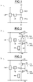
- references DIS1 and DIS2 designate electronic devices for protecting at least one component or an electronic module CMP of an integrated electronic circuit CI against electrostatic discharges ("Electrostatic Discharges": ESD according to an Anglo-Saxon acronym well known to those skilled in the art).
- the electronic circuit CI comprises a supply terminal B1, a reference terminal B2 and a signal terminal B3, and the component CMP is coupled to each of these three terminals B1, B2, and B3.
- the power supply terminal B1 can receive a power supply signal, for example a positive voltage
- the B2 terminal can receive a reference signal, for example a constant negative voltage or a zero voltage.
- the B3 signal terminal can receive or transmit a data signal from or to the CMP module.
- the circuit IC When the circuit IC is not in operation, the circuit IC can be subjected to electrostatic discharges circulating between one or the other of these terminals.
- An electrostatic discharge conventionally results in a very brief current pulse (for example a few microseconds) whose amplitude is for example of the order of 2 amperes and typically occurs after 10 nanoseconds.
- HBM are the abbreviation of the Anglo-Saxon acronym "Human Body Model” well known to those skilled in the art in the field of protection against electrostatic discharges and designate in particular an electrical circuit aimed at modeling an electrostatic discharge delivered by a human being and usually used to test the sensitivity of devices to electrostatic discharges.
- This HBM electrical circuit which is the equivalent R-L-C circuit mentioned above and to which a high voltage is applied, comprises in particular a 100 pF capacitor which discharges through a 1.5 kilo-ohm resistor in the device to be tested.
- an electrostatic discharge of 4 kilovolts HBM means that a potential difference of 4 kilovolts is applied to the electric circuit HBM.
- This current pulse should then flow through one of the protection devices DIS1 and DIS2 and not through the component CMP.
- the devices DIS1 and DIS2 therefore aim to absorb these current pulses occurring respectively between the supply terminal B1 and the signal terminal, and between the reference terminal and the signal terminal, or between the two terminals B1 and B2.
- the devices DIS1 and DIS2 respectively comprise a first MOS transistor TR1 and a second MOS transistor TR2, connected in series between the supply terminal B1 and the reference terminal B2.
- the drain D1 of the first transistor TR1 is coupled to the supply terminal B1
- the source S1 of the first transistor TR1 is coupled to the signal terminal B3 and the drain D2 of the second transistor TR2
- the source S2 of the second transistor TR2 is coupled to reference terminal B2.
- Gate G1 of first transistor TR1 and gate G2 of second transistor TR2 are directly coupled to reference terminal B2.
- a direct connection or coupling is understood here as being a connection not involving an active or passive intermediate component, but only elements whose sole function is to transmit the signal, such as metal tracks, vias, etc. .
- the first transistor TR1 is thus in a configuration commonly designated by those skilled in the art by the acronym “GGNMOS” (Gate Grounded NMOS).
- the substrate sb1 of the first transistor TR1 and the substrate sb2 of the second transistor TR2 are here coupled to the reference terminal B2, via a common resistor R1.
- the common resistor R1 has in this embodiment a resistive value of 500 ohms.
- the first transistor TR1 and the second transistor TR2 are made on one and the same substrate, as will be seen below.
- the substrate sb1 which here corresponds to the base of the parasitic bipolar transistor of the first MOS transistor TR1, is therefore biased and the parasitic bipolar transistor (and therefore the first MOS transistor TR1) turns on.
- the transistor TR1 triggers here when the voltage across its terminals reaches 4.5 volts.
- the substrate sb1 which here corresponds to the base of the parasitic bipolar transistor of the first MOS transistor TR1, is therefore biased and the parasitic bipolar transistor (and therefore the first MOS transistor TR1) turns on.
- the triggering of the device DIS1 is more progressive, that is to say that for a voltage value at its terminals of less than 2.5 volts, the current intensity through the device DIS1 increases linearly , and beyond 2.5 volts, the intensity of the current passing through the first device DIS1 increases exponentially, while the voltage across the terminals of the first transistor TR1 approaches asymptotically 3.5 volts.
- the substrate sb2 which here corresponds to the base of the parasitic bipolar transistor of the second MOS transistor TR2, is therefore biased and the parasitic bipolar transistor (and therefore the second MOS transistor TR2) turns on.
- the second transistor TR2 has a configuration of the GGNMOS type, and the reference terminal B2 to which its gate G2 and its substrate sb2 are connected acts here as ground.
- the second transistor TR2 is triggered here for a voltage across its terminals equal to 4.2 volts.
- the second transistor TR2 triggers in a conventional manner, as soon as its gate-source voltage exceeds its threshold voltage.
- the biasing of the substrate sb2 makes it possible to lower the threshold voltage of the second transistor TR2.
- the transistor triggers for a voltage of 0.6 volts.
- the voltage generated by the electrostatic discharge increases until it reaches the breakdown voltage of the drain-substrate junction of the first transistor TR1 .
- Substrate sb1 which here corresponds to the base of the parasitic bipolar transistor of the first MOS transistor TR1, is therefore biased and the parasitic bipolar transistor of the first MOS transistor TR1 turns on.
- Substrate sb2 of second MOS transistor TR2 is also biased due to the connection between substrates sb1 and sb2, and the parasitic bipolar transistor of second MOS transistor TR2 also turns on.
- the first MOS transistor TR1 and the second transistor TR2 then trigger for a voltage between the terminals B1 and B2 of a value of 4.2 volts.
- the discharge is transmitted simultaneously to the gate G1 of the first transistor TR1, to the gate G2 of the second transistor TR2, to the substrate sb1 of the first transistor TR1 and on the substrate sb2 of the second transistor TR2.
- the two transistors TR1 and TR2 therefore trigger in a conventional manner in order to cause the electrostatic discharge to circulate.
- the CMP component is protected against electrostatic discharges that may occur between any two of its three terminals B1, B2 and B3.
- connection of the substrate sb1 and of the gate G1 of the first transistor TR1 to a reference terminal B2, that is to say to a different terminal from the signal terminal B3, makes it possible to avoid, when the device is in operation and that for example the potential difference between the supply terminal and the signal terminal is higher than the triggering threshold of transistor TR1, that the gate G1 of the first transistor TR1 is biased and that the first transistor TR1 is triggered.
- the gate G1 of the first transistor TR1 and the gate G2 of the second transistor TR2 to be coupled to the reference terminal via the common resistor R1.
- each transistor has its gate and its substrate mutually connected.
- the common resistor R1 and the drain-gate capacitor of the first MOS transistor TR1 form a first resistive-capacitive trigger enabling the electrostatic pulse to be transmitted to the gate of the first MOS transistor TR1.
- the electrostatic pulse will be transmitted both to the gate G1 via the drain-gate or source-gate capacitors, and to the substrate sb1 of the first MOS transistor TR1 by breakdown of the drain-substrate or source-substrate junction.
- the common resistor R1 and the drain-gate capacitance of the second MOS transistor TR2 form a first resistive-capacitive trigger enabling the electrostatic pulse to be transmitted to the gate of the second MOS transistor TR2.
- the electrostatic pulse will be transmitted both to the gate G2 via the drain-gate or source-gate capacitors, and to the substrate sb2 of the second MOS transistor TR2 by breakdown of the drain-substrate or source-substrate junction.
- the presence of the connection between the gate and the substrate of each transistor allows the gate to polarize more and therefore to amplify the combined MOS and bipolar effects, because the closer the gate voltage is to the threshold voltage of the MOS transistor, the more the current gain increases.
- connection of the substrate sb1 and the gate G1 of the first transistor TR1, through the common resistor R1, to the reference terminal B2, i.e. to a different terminal of the signal terminal B3, makes it possible to avoid, when the device is in operation and that for example the potential difference between the supply terminal and the signal terminal is greater than the triggering threshold of the transistor TR1, that the gate G1 of the first transistor TR1 is biased and the first transistor TR1 triggers.
- This device comprises a third transistor TR3, whose gate G3 can be directly connected to the reference terminal ( figure 5 ) or indirectly via the common resistor R1 ( figure 6 ).
- the voltage generated by the current pulse increases until it reaches the breakdown voltage of the drain-substrate junction of the third transistor MOS TR3.
- the third transistor TR3 has a configuration of the GGNMOS type, and the reference terminal B2, to which the gate G3 of the third MOS transistor TR3 is connected, acts here as ground.
- the transistor triggers for a voltage across its terminals equal to 4.2 volts.
- the propagation path of the electrostatic discharge is more direct than if the discharge flowed from the supply terminal B1 to the reference terminal B2 via the first transistor TR1 and the second MOS transistor TR2, which makes it possible to avoid the presence of overvoltages due to the circulation of the current pulse through the two transistors whose resistive value is not zero.
- the current pulse is transmitted through the common resistor R1 on the substrate sb3 of the third MOS transistor TR3, and through the direct connection on gate G3 of MOS transistor TR3.
- the third transistor TR3 triggers conventionally, as soon as its gate-source voltage exceeds its threshold voltage.
- the biasing of the substrate sb3 of the third MOS transistor TR3 makes it possible to lower the threshold voltage of the third transistor TR3.
- the third MOS transistor TR3 triggers for a voltage of 0.6 volts.
- the propagation path is more direct than if the pulse circulated between the reference terminal B2 and the signal terminal B1 via the first MOS transistor TR1 and the second MOS transistor TR2.
- the triggering threshold of the third MOS transistor TR3 is lowered to 1.5 volts in the case of a discharge flowing from the supply terminal B1 to the reference terminal B2.
- the circuit CI is thus protected against the electrostatic discharges circulating between the supply terminal B1 and the reference terminal B2.
- the protection devices DIS1, DIS2 and DIS3 can be produced in parallel with existing protection devices, for example diodes or thyristors.
- two thyristors 1 and 2 mounted head to tail are coupled between the supply terminal B1 and the reference terminal B2.
- the production of the protection devices DIS1, DIS2 and DIS3 is therefore compatible with existing manufacturing methods which include the production of other protection means.
- the existing devices can either operate in parallel with the devices DIS1, DIS2 and/or DIS 3, or be inhibited by the devices DIS1, DIS2 and/or DIS3.
- the integrated circuit CI comprises a plurality of signal terminals, of which a first signal terminal B3 and a second signal terminal B4 would be indirectly connected via an electronic module CMP2.
- the integrated circuit CI comprises a fourth protection device DIS4 coupled between the first signal terminal B3 and the second signal terminal B4.
- the fourth protection device may comprise a fourth MOS transistor TR4, whose gate G4 is directly coupled to the reference terminal B2, and whose substrate sb4 is coupled to the reference terminal via the common resistor R1.
- the substrate sb4 of the intermediate transistor TR4 could be coupled to the second signal terminal B4 via the common resistor R2 to the protection circuits associated with the second signal terminal B4.
- the fourth transistor TR4 here has a GGNMOS type configuration.
- the voltage generated by the current pulse increases until it reaches the breakdown voltage of the drain-substrate junction of the fourth MOS transistor TR4.
- Substrate sb4 which here corresponds to the base of the parasitic bipolar transistor of the fourth MOS transistor TR4, is therefore biased and the parasitic bipolar transistor of the fourth transistor TR4 turns on.
- the intermediate transistor TR4 it would be possible for the intermediate transistor TR4 to be a transistor in a configuration allowing hybrid operation, having its gate G4 and its substrate sb4 mutually directly connected and coupled to the reference terminal B2 via the common resistor R1 .
- This configuration makes it possible to further improve the triggering of the fourth transistor TR4.
- the figure 10 illustrates a top view of an integrated circuit CI comprising the first transistor TR1, the second transistor TR2, the third transistor TR3, and the common resistor R1 according to the embodiment described above in connection with the figure 5 .
- the three transistors are made on a single and same substrate sb, delimited by an insulation trench STI and are made in such a way as to share at least one of their electrodes.
- each transistor is made in duplicate, that is to say that it actually comprises two identical transistors mounted in parallel. This is equivalent to a transistor of larger in size, which makes it possible to withstand the passage of the current pulse resulting from an electrostatic discharge.
- each transistor could comprise any number of identical transistors connected in parallel, the size of the equivalent transistor being all the greater as the number of identical transistors is high.
- the drain D1 of the first transistor TR1 and the drain D3 of the third transistor TR3 are combined and connected to the supply terminal B1 via vias and metal tracks
- the source S3 of the third transistor TR3 and the source S2 of the second transistor TR2 are merged and connected to the reference terminal B2 via vias and metal tracks
- the source S1 of the first transistor TR1 and the drain D2 of the second transistor TR2 are merged and connected to the signal terminal B3 .
- the gates G1, G2 and G3 are mutually connected and coupled to the second terminal B2 via vias and metal tracks. However, they could be connected to the common resistor R1 via vias and metal tracks.
- the substrate of each transistor is coupled to the common resistor R1 via vias and metal tracks.
- the substrate can be a solid substrate or a silicon-on-insulator (SOI: Silicon On Insulator) type substrate.
- SOI Silicon On Insulator
Landscapes
- Engineering & Computer Science (AREA)
- Microelectronics & Electronic Packaging (AREA)
- Semiconductor Integrated Circuits (AREA)
- Metal-Oxide And Bipolar Metal-Oxide Semiconductor Integrated Circuits (AREA)
Claims (11)
- Integrierter Schaltkreis, eine Einspeiseklemme (B1) enthaltend, die dazu bestimmt ist, eine Einspeisespannung zu empfangen, eine Referenzklemme (B2), die dazu bestimmt ist, eine Referenzspannung zu empfangen und mindestens eine Signalklemme (B3), die dazu bestimmt ist, ein Signal zu empfangen/zu senden, eine erste Schutzvorrichtung (DIS1), die zwischen die mindestens eine Signalklemme (B3) und die Einspeiseklemme (B1) gekoppelt ist, und mindestens eine zweite Schutzvorrichtung (DIS2), die zwischen die mindestens eine Signalklemme (B3) und die Referenzklemme (B2) gekoppelt ist, wobei die erste Schutzvorrichtung (DIS1) einen ersten MOS-Transistor (TR1) umfasst, dessen erste Elektrode (S1) mit der mindestens einen Signalklemme (B3) gekoppelt ist und eine zweite Elektrode (D1) mit der Einspeiseklemme (B1) gekoppelt ist, wobei die mindestens eine zweite Schutzvorrichtung (DIS2) einen zweiten MOS-Transistor (TR2) enthält, dessen erste Elektrode (D2) mit der mindestens einen Signalklemme (B3) gekoppelt ist und eine zweite Elektrode (S2) mit der Referenzklemme (B2) gekoppelt ist, wobei die Gates (G1, G2) der ersten und zweiten MOS-Transistoren (TR1, TR2) direkt oder indirekt mit der Referenzklemme (B2) gekoppelt sind, und wobei die Substrate (sbl, sb2) des ersten und zweiten MOS-Transistors (TR1, TR2) über einen gemeinsamen Widerstand (R1) mit der Referenzklemme (B2) gekoppelt sind, dadurch gekennzeichnet, dass der gemeinsame Widerstand (R1) von den Substraten (sbl, sb2) getrennt ist.
- Integrierter Schaltkreis nach Anspruch 1, wobei die Gates (G1, G2) des ersten und zweiten MOS-Transistors (TR1, TR2) direkt mit der Referenzklemme (B2) gekoppelt sind.
- Integrierter Schaltkreis nach Anspruch 1, wobei die Gates (G1, G2) des ersten und zweiten MOS-Transistors (TR1, TR2) über eine erste Auslöseschaltung (R1) mit der Referenzklemme (B2) gekoppelt sind.
- Integrierter Schaltkreis nach Anspruch 3, wobei die erste Auslöseschaltung den gemeinsamen Widerstand (R1) umfasst.
- Integrierter Schaltkreis nach einem der Ansprüche 1 bis 4, eine dritte Schutzvorrichtung (DIS3) enthaltend, die zwischen die Einspeiseklemme (B1) und die Referenzklemme (B2) gekoppelt ist und einen dritten MOS-Transistor (TR3) umfassend, dessen erste Elektrode (D3) mit der Einspeiseklemme (B1) gekoppelt ist und eine zweite Elektrode (S3) mit der Referenzklemme (B2) gekoppelt ist, und dessen Gate (G3) direkt mit der Referenzklemme (B2) gekoppelt ist und das Substrat (sb3) über den gemeinsamen Widerstand (R1) mit der Referenzklemme gekoppelt ist.
- Integrierter Schaltkreis nach einem der Ansprüche 1 bis 4, eine dritte Schutzvorrichtung (DIS3) enthaltend, die zwischen die Einspeiseklemme (B1) und die Referenzklemme (B2) gekoppelt ist, und einen dritten MOS-Transistor (TR3) umfassend, dessen erste Elektrode (D3) mit der Einspeiseklemme (B1) gekoppelt ist, und eine zweite Elektrode (S3) mit der Referenzklemme (B2) gekoppelt ist, dessen Substrat (sb3) über den gemeinsamen Widerstand (R1) mit der Referenzklemme (B2) gekoppelt ist, und dessen Gate (G3) über eine zweite Auslöseschaltung mit der Referenzklemme (B2) gekoppelt ist.
- Integrierter Schaltkreis nach Anspruch 6, wobei die zweite Auslöseschaltung den gemeinsamen Widerstand (R1) umfasst.
- Integrierter Schaltkreis nach einem der vorhergehenden Ansprüche, eine erste Signalklemme (B3) und mindestens eine zweite Signalklemme (B4) umfassend, und mindestens eine vierte Schutzvorrichtung (DIS4), die zwischen die erste Signalklemme (B3) und die zweite Signalklemme (B4) gekoppelt ist und einen vierten MOS-Transistor (TR4) umfassend, dessen erste Elektrode mit der ersten Signalklemme (B3) gekoppelt ist, eine zweite Elektrode mit der zweiten Signalklemme (B4) gekoppelt ist, dessen Gate (G4) direkt mit der Referenzklemme (B2) gekoppelt ist, und dessen Substrat (sb4) über den gemeinsamen Widerstand (R1) mit der Referenzklemme (B2) gekoppelt ist.
- Integrierter Schaltkreis nach einem der Ansprüche 1 bis 7, eine erste Signalklemme (B3) und mindestens eine zweite Signalklemme (B4) umfassend, und mindestens eine vierte Schutzvorrichtung (DIS4), die zwischen die erste Signalklemme (B3) und die zweite Signalklemme (B4) gekoppelt ist und einen vierten MOS-Transistor (TR4) umfassend, dessen erste Elektrode mit der ersten Signalklemme gekoppelt ist und eine zweite Elektrode mit der zweiten Signalklemme gekoppelt ist, und dessen Substrat (sb4) über den gemeinsamen Widerstand (R1) mit der Referenzklemme (B2) gekoppelt ist und dessen Gate (G4) über eine dritte Auslöseschaltung mit der Referenzklemme (B2) gekoppelt ist.
- Integrierter Schaltkreis nach Anspruch 9, wobei die dritte Auslöseschaltung den gemeinsamen Widerstand (R1) enthält.
- Integrierter Schaltkreis nach einem der vorhergehenden Ansprüche, wobei die MOS-Transistoren (TR1, TR2, TR3, TR4) in einem einzigen Substrat (sb) ausgeführt sind und miteinander verbundene Gate aufweisen.
Applications Claiming Priority (1)
| Application Number | Priority Date | Filing Date | Title |
|---|---|---|---|
| FR1751731A FR3063574B1 (fr) | 2017-03-03 | 2017-03-03 | Dispositif compact de protection d'un circuit integre contre les decharges electrostatiques |
Publications (2)
| Publication Number | Publication Date |
|---|---|
| EP3370256A1 EP3370256A1 (de) | 2018-09-05 |
| EP3370256B1 true EP3370256B1 (de) | 2022-07-13 |
Family
ID=58993015
Family Applications (1)
| Application Number | Title | Priority Date | Filing Date |
|---|---|---|---|
| EP17186784.9A Active EP3370256B1 (de) | 2017-03-03 | 2017-08-18 | Kompakte vorrichtung zum schutz eines integrierten schaltkreises gegen elektrostatische entladungen |
Country Status (3)
| Country | Link |
|---|---|
| US (3) | US10340265B2 (de) |
| EP (1) | EP3370256B1 (de) |
| FR (1) | FR3063574B1 (de) |
Families Citing this family (1)
| Publication number | Priority date | Publication date | Assignee | Title |
|---|---|---|---|---|
| US12474399B2 (en) * | 2023-04-19 | 2025-11-18 | Nxp B.V. | Analog test devices for integrated circuits with multiple power domains |
Family Cites Families (11)
| Publication number | Priority date | Publication date | Assignee | Title |
|---|---|---|---|---|
| KR970072681A (ko) * | 1996-04-03 | 1997-11-07 | 김광호 | 기판 바이어스가 분리된 회로에서의 정전기 보호회로 |
| US6249410B1 (en) * | 1999-08-23 | 2001-06-19 | Taiwan Semiconductor Manufacturing Company | ESD protection circuit without overstress gate-driven effect |
| TW560038B (en) * | 2002-05-29 | 2003-11-01 | Ind Tech Res Inst | Electrostatic discharge protection circuit using whole chip trigger technique |
| US20040257728A1 (en) * | 2003-06-20 | 2004-12-23 | Hu David Yu | Electrostatic discharge protection device and network with high voltage tolerance |
| US20090040668A1 (en) * | 2007-08-10 | 2009-02-12 | Zi-Ping Chen | Esd protection circuits for mixed-voltage buffers |
| JP4516102B2 (ja) * | 2007-09-26 | 2010-08-04 | 株式会社東芝 | Esd保護回路 |
| JP2010080622A (ja) * | 2008-09-25 | 2010-04-08 | Panasonic Corp | 半導体集積回路 |
| US9385241B2 (en) * | 2009-07-08 | 2016-07-05 | Taiwan Semiconductor Manufacturing Company, Ltd. | Electrostatic discharge (ESD) protection circuits, integrated circuits, systems, and methods for forming the ESD protection circuits |
| WO2011089179A1 (fr) * | 2010-01-22 | 2011-07-28 | Stmicroelectronics Sa | Dispositif electronique, en particulier de protection contre les décharges électrostatistiques, et procédé de protection d'un composant contre des décharges électrostatiques |
| FR2982720B1 (fr) * | 2011-11-15 | 2014-01-03 | St Microelectronics Sa | Interrupteur de puissance |
| US9054793B2 (en) * | 2013-07-19 | 2015-06-09 | International Business Machines Corporation | Structure, system and method for device radio frequency (RF) reliability |
-
2017
- 2017-03-03 FR FR1751731A patent/FR3063574B1/fr not_active Expired - Fee Related
- 2017-08-18 EP EP17186784.9A patent/EP3370256B1/de active Active
- 2017-09-01 US US15/694,403 patent/US10340265B2/en active Active
-
2019
- 2019-05-08 US US16/406,534 patent/US10971489B2/en active Active
-
2021
- 2021-03-03 US US17/191,250 patent/US11887982B2/en active Active
Also Published As
| Publication number | Publication date |
|---|---|
| US10340265B2 (en) | 2019-07-02 |
| FR3063574A1 (fr) | 2018-09-07 |
| US10971489B2 (en) | 2021-04-06 |
| US20180254270A1 (en) | 2018-09-06 |
| EP3370256A1 (de) | 2018-09-05 |
| US11887982B2 (en) | 2024-01-30 |
| US20210193648A1 (en) | 2021-06-24 |
| FR3063574B1 (fr) | 2019-05-03 |
| US20190267367A1 (en) | 2019-08-29 |
Similar Documents
| Publication | Publication Date | Title |
|---|---|---|
| EP3465755B1 (de) | Integrierte schaltung mit einem durch einen hochspannungstransistor gebildeten chip und mit einem durch einen niedrigspannungstransistor gebildeten chip | |
| WO2011089179A1 (fr) | Dispositif electronique, en particulier de protection contre les décharges électrostatistiques, et procédé de protection d'un composant contre des décharges électrostatiques | |
| FR2685817A1 (fr) | Protection generale d'un circuit integre contre les surcharges permanentes et decharges electrostatiques. | |
| FR2984604A1 (fr) | Dispositif electronique compact de protection contre les decharges electrostatiques. | |
| FR2982416A1 (fr) | Dispositif electronique de protection contre les decharges electrostatiques | |
| FR2987496A1 (fr) | Circuit de protection contre les decharges electrostatiques | |
| FR3016999A1 (fr) | Dispositif electronique, en particulier pour la protection contre les decharges electrostatiques | |
| EP2290691A1 (de) | Schutzvorrichtung für einen integrierten Schaltkreis gegen elektrostatische Entladungen | |
| FR2673494A1 (fr) | Module de commutation, matrice de commutateurs et systeme de commutation d'impulsion de grande intensite. | |
| EP3961345A1 (de) | Stromzufuhr zu einem elektronischen schaltkreis | |
| EP3961344A1 (de) | Stromzufuhr zu einem elektronischen schaltkreis | |
| FR2948828A1 (fr) | Dispositif electronique de protection contre une inversion de polarite d'une tension d'alimentation continue, et application au domaine de l'automobile | |
| FR3064383A1 (fr) | Dispositif integre de neurone artificiel | |
| FR3057394A1 (fr) | Dispositif de protection contre les decharges electrostatiques avec circuit de declenchement distribue | |
| FR3038131A1 (fr) | Dispositif de protection ameliore contre les decharges electrostatiques. | |
| EP3731414B1 (de) | Eingangs-ausgangsschaltung umfassend eine schutzschaltung mit einer reihenschaltung von transistoren, und verfahren zum steuern der schaltung | |
| EP3370256B1 (de) | Kompakte vorrichtung zum schutz eines integrierten schaltkreises gegen elektrostatische entladungen | |
| EP3863140A1 (de) | Schutz gegen überspannungen | |
| FR2975224A1 (fr) | Dispositif de protection haute performance contre des decharges electrostatiques | |
| EP2348528A1 (de) | Schutzvorrichtung für einen integrierten Schaltkreis gegen elektrostatische Entladungen | |
| FR3072481B1 (fr) | Dispositif de generation d'un signal aleatoire | |
| FR3131981A1 (fr) | Dispositif de protection contre les décharges électrostatiques | |
| FR2795557A1 (fr) | Dispositif d'ajustement des circuits apres mise en boitier et procede de fabrication correspondant | |
| EP4184579B1 (de) | Schutz einer domäne einer integrierten schaltung gegen überspannungen | |
| EP4459677A1 (de) | Schutzvorrichtung gegen elektrostatische entladungen |
Legal Events
| Date | Code | Title | Description |
|---|---|---|---|
| PUAI | Public reference made under article 153(3) epc to a published international application that has entered the european phase |
Free format text: ORIGINAL CODE: 0009012 |
|
| STAA | Information on the status of an ep patent application or granted ep patent |
Free format text: STATUS: REQUEST FOR EXAMINATION WAS MADE |
|
| 17P | Request for examination filed |
Effective date: 20170818 |
|
| AK | Designated contracting states |
Kind code of ref document: A1 Designated state(s): AL AT BE BG CH CY CZ DE DK EE ES FI FR GB GR HR HU IE IS IT LI LT LU LV MC MK MT NL NO PL PT RO RS SE SI SK SM TR |
|
| AX | Request for extension of the european patent |
Extension state: BA ME |
|
| STAA | Information on the status of an ep patent application or granted ep patent |
Free format text: STATUS: EXAMINATION IS IN PROGRESS |
|
| 17Q | First examination report despatched |
Effective date: 20200504 |
|
| RIC1 | Information provided on ipc code assigned before grant |
Ipc: H02H 9/04 20060101ALI20220114BHEP Ipc: H01L 49/02 20060101ALI20220114BHEP Ipc: H01L 27/02 20060101AFI20220114BHEP |
|
| GRAP | Despatch of communication of intention to grant a patent |
Free format text: ORIGINAL CODE: EPIDOSNIGR1 |
|
| STAA | Information on the status of an ep patent application or granted ep patent |
Free format text: STATUS: GRANT OF PATENT IS INTENDED |
|
| INTG | Intention to grant announced |
Effective date: 20220303 |
|
| GRAS | Grant fee paid |
Free format text: ORIGINAL CODE: EPIDOSNIGR3 |
|
| GRAA | (expected) grant |
Free format text: ORIGINAL CODE: 0009210 |
|
| STAA | Information on the status of an ep patent application or granted ep patent |
Free format text: STATUS: THE PATENT HAS BEEN GRANTED |
|
| AK | Designated contracting states |
Kind code of ref document: B1 Designated state(s): AL AT BE BG CH CY CZ DE DK EE ES FI FR GB GR HR HU IE IS IT LI LT LU LV MC MK MT NL NO PL PT RO RS SE SI SK SM TR |
|
| REG | Reference to a national code |
Ref country code: CH Ref legal event code: EP |
|
| REG | Reference to a national code |
Ref country code: DE Ref legal event code: R096 Ref document number: 602017059402 Country of ref document: DE |
|
| REG | Reference to a national code |
Ref country code: AT Ref legal event code: REF Ref document number: 1504709 Country of ref document: AT Kind code of ref document: T Effective date: 20220815 |
|
| REG | Reference to a national code |
Ref country code: IE Ref legal event code: FG4D Free format text: LANGUAGE OF EP DOCUMENT: FRENCH |
|
| REG | Reference to a national code |
Ref country code: LT Ref legal event code: MG9D |
|
| REG | Reference to a national code |
Ref country code: NL Ref legal event code: MP Effective date: 20220713 |
|
| PG25 | Lapsed in a contracting state [announced via postgrant information from national office to epo] |
Ref country code: SE Free format text: LAPSE BECAUSE OF FAILURE TO SUBMIT A TRANSLATION OF THE DESCRIPTION OR TO PAY THE FEE WITHIN THE PRESCRIBED TIME-LIMIT Effective date: 20220713 Ref country code: RS Free format text: LAPSE BECAUSE OF FAILURE TO SUBMIT A TRANSLATION OF THE DESCRIPTION OR TO PAY THE FEE WITHIN THE PRESCRIBED TIME-LIMIT Effective date: 20220713 Ref country code: PT Free format text: LAPSE BECAUSE OF FAILURE TO SUBMIT A TRANSLATION OF THE DESCRIPTION OR TO PAY THE FEE WITHIN THE PRESCRIBED TIME-LIMIT Effective date: 20221114 Ref country code: NO Free format text: LAPSE BECAUSE OF FAILURE TO SUBMIT A TRANSLATION OF THE DESCRIPTION OR TO PAY THE FEE WITHIN THE PRESCRIBED TIME-LIMIT Effective date: 20221013 Ref country code: NL Free format text: LAPSE BECAUSE OF FAILURE TO SUBMIT A TRANSLATION OF THE DESCRIPTION OR TO PAY THE FEE WITHIN THE PRESCRIBED TIME-LIMIT Effective date: 20220713 Ref country code: LV Free format text: LAPSE BECAUSE OF FAILURE TO SUBMIT A TRANSLATION OF THE DESCRIPTION OR TO PAY THE FEE WITHIN THE PRESCRIBED TIME-LIMIT Effective date: 20220713 Ref country code: LT Free format text: LAPSE BECAUSE OF FAILURE TO SUBMIT A TRANSLATION OF THE DESCRIPTION OR TO PAY THE FEE WITHIN THE PRESCRIBED TIME-LIMIT Effective date: 20220713 Ref country code: FI Free format text: LAPSE BECAUSE OF FAILURE TO SUBMIT A TRANSLATION OF THE DESCRIPTION OR TO PAY THE FEE WITHIN THE PRESCRIBED TIME-LIMIT Effective date: 20220713 Ref country code: ES Free format text: LAPSE BECAUSE OF FAILURE TO SUBMIT A TRANSLATION OF THE DESCRIPTION OR TO PAY THE FEE WITHIN THE PRESCRIBED TIME-LIMIT Effective date: 20220713 |
|
| REG | Reference to a national code |
Ref country code: AT Ref legal event code: MK05 Ref document number: 1504709 Country of ref document: AT Kind code of ref document: T Effective date: 20220713 |
|
| PG25 | Lapsed in a contracting state [announced via postgrant information from national office to epo] |
Ref country code: PL Free format text: LAPSE BECAUSE OF FAILURE TO SUBMIT A TRANSLATION OF THE DESCRIPTION OR TO PAY THE FEE WITHIN THE PRESCRIBED TIME-LIMIT Effective date: 20220713 Ref country code: IS Free format text: LAPSE BECAUSE OF FAILURE TO SUBMIT A TRANSLATION OF THE DESCRIPTION OR TO PAY THE FEE WITHIN THE PRESCRIBED TIME-LIMIT Effective date: 20221113 Ref country code: HR Free format text: LAPSE BECAUSE OF FAILURE TO SUBMIT A TRANSLATION OF THE DESCRIPTION OR TO PAY THE FEE WITHIN THE PRESCRIBED TIME-LIMIT Effective date: 20220713 Ref country code: GR Free format text: LAPSE BECAUSE OF FAILURE TO SUBMIT A TRANSLATION OF THE DESCRIPTION OR TO PAY THE FEE WITHIN THE PRESCRIBED TIME-LIMIT Effective date: 20221014 |
|
| REG | Reference to a national code |
Ref country code: CH Ref legal event code: PL |
|
| REG | Reference to a national code |
Ref country code: DE Ref legal event code: R097 Ref document number: 602017059402 Country of ref document: DE |
|
| PG25 | Lapsed in a contracting state [announced via postgrant information from national office to epo] |
Ref country code: SM Free format text: LAPSE BECAUSE OF FAILURE TO SUBMIT A TRANSLATION OF THE DESCRIPTION OR TO PAY THE FEE WITHIN THE PRESCRIBED TIME-LIMIT Effective date: 20220713 Ref country code: RO Free format text: LAPSE BECAUSE OF FAILURE TO SUBMIT A TRANSLATION OF THE DESCRIPTION OR TO PAY THE FEE WITHIN THE PRESCRIBED TIME-LIMIT Effective date: 20220713 Ref country code: MC Free format text: LAPSE BECAUSE OF FAILURE TO SUBMIT A TRANSLATION OF THE DESCRIPTION OR TO PAY THE FEE WITHIN THE PRESCRIBED TIME-LIMIT Effective date: 20220713 Ref country code: LU Free format text: LAPSE BECAUSE OF NON-PAYMENT OF DUE FEES Effective date: 20220818 Ref country code: LI Free format text: LAPSE BECAUSE OF NON-PAYMENT OF DUE FEES Effective date: 20220831 Ref country code: DK Free format text: LAPSE BECAUSE OF FAILURE TO SUBMIT A TRANSLATION OF THE DESCRIPTION OR TO PAY THE FEE WITHIN THE PRESCRIBED TIME-LIMIT Effective date: 20220713 Ref country code: CZ Free format text: LAPSE BECAUSE OF FAILURE TO SUBMIT A TRANSLATION OF THE DESCRIPTION OR TO PAY THE FEE WITHIN THE PRESCRIBED TIME-LIMIT Effective date: 20220713 Ref country code: CH Free format text: LAPSE BECAUSE OF NON-PAYMENT OF DUE FEES Effective date: 20220831 Ref country code: AT Free format text: LAPSE BECAUSE OF FAILURE TO SUBMIT A TRANSLATION OF THE DESCRIPTION OR TO PAY THE FEE WITHIN THE PRESCRIBED TIME-LIMIT Effective date: 20220713 |
|
| REG | Reference to a national code |
Ref country code: BE Ref legal event code: MM Effective date: 20220831 |
|
| PLBE | No opposition filed within time limit |
Free format text: ORIGINAL CODE: 0009261 |
|
| STAA | Information on the status of an ep patent application or granted ep patent |
Free format text: STATUS: NO OPPOSITION FILED WITHIN TIME LIMIT |
|
| PG25 | Lapsed in a contracting state [announced via postgrant information from national office to epo] |
Ref country code: SK Free format text: LAPSE BECAUSE OF FAILURE TO SUBMIT A TRANSLATION OF THE DESCRIPTION OR TO PAY THE FEE WITHIN THE PRESCRIBED TIME-LIMIT Effective date: 20220713 Ref country code: EE Free format text: LAPSE BECAUSE OF FAILURE TO SUBMIT A TRANSLATION OF THE DESCRIPTION OR TO PAY THE FEE WITHIN THE PRESCRIBED TIME-LIMIT Effective date: 20220713 |
|
| 26N | No opposition filed |
Effective date: 20230414 |
|
| GBPC | Gb: european patent ceased through non-payment of renewal fee |
Effective date: 20221013 |
|
| PG25 | Lapsed in a contracting state [announced via postgrant information from national office to epo] |
Ref country code: AL Free format text: LAPSE BECAUSE OF FAILURE TO SUBMIT A TRANSLATION OF THE DESCRIPTION OR TO PAY THE FEE WITHIN THE PRESCRIBED TIME-LIMIT Effective date: 20220713 |
|
| PG25 | Lapsed in a contracting state [announced via postgrant information from national office to epo] |
Ref country code: IE Free format text: LAPSE BECAUSE OF NON-PAYMENT OF DUE FEES Effective date: 20220818 Ref country code: FR Free format text: LAPSE BECAUSE OF NON-PAYMENT OF DUE FEES Effective date: 20220913 |
|
| PG25 | Lapsed in a contracting state [announced via postgrant information from national office to epo] |
Ref country code: SI Free format text: LAPSE BECAUSE OF FAILURE TO SUBMIT A TRANSLATION OF THE DESCRIPTION OR TO PAY THE FEE WITHIN THE PRESCRIBED TIME-LIMIT Effective date: 20220713 |
|
| PG25 | Lapsed in a contracting state [announced via postgrant information from national office to epo] |
Ref country code: BE Free format text: LAPSE BECAUSE OF NON-PAYMENT OF DUE FEES Effective date: 20220831 |
|
| PG25 | Lapsed in a contracting state [announced via postgrant information from national office to epo] |
Ref country code: GB Free format text: LAPSE BECAUSE OF NON-PAYMENT OF DUE FEES Effective date: 20221013 |
|
| PG25 | Lapsed in a contracting state [announced via postgrant information from national office to epo] |
Ref country code: IT Free format text: LAPSE BECAUSE OF FAILURE TO SUBMIT A TRANSLATION OF THE DESCRIPTION OR TO PAY THE FEE WITHIN THE PRESCRIBED TIME-LIMIT Effective date: 20220713 |
|
| PG25 | Lapsed in a contracting state [announced via postgrant information from national office to epo] |
Ref country code: HU Free format text: LAPSE BECAUSE OF FAILURE TO SUBMIT A TRANSLATION OF THE DESCRIPTION OR TO PAY THE FEE WITHIN THE PRESCRIBED TIME-LIMIT; INVALID AB INITIO Effective date: 20170818 |
|
| PG25 | Lapsed in a contracting state [announced via postgrant information from national office to epo] |
Ref country code: CY Free format text: LAPSE BECAUSE OF FAILURE TO SUBMIT A TRANSLATION OF THE DESCRIPTION OR TO PAY THE FEE WITHIN THE PRESCRIBED TIME-LIMIT Effective date: 20220713 |
|
| PG25 | Lapsed in a contracting state [announced via postgrant information from national office to epo] |
Ref country code: MK Free format text: LAPSE BECAUSE OF FAILURE TO SUBMIT A TRANSLATION OF THE DESCRIPTION OR TO PAY THE FEE WITHIN THE PRESCRIBED TIME-LIMIT Effective date: 20220713 |
|
| PG25 | Lapsed in a contracting state [announced via postgrant information from national office to epo] |
Ref country code: BG Free format text: LAPSE BECAUSE OF FAILURE TO SUBMIT A TRANSLATION OF THE DESCRIPTION OR TO PAY THE FEE WITHIN THE PRESCRIBED TIME-LIMIT Effective date: 20220713 |
|
| PG25 | Lapsed in a contracting state [announced via postgrant information from national office to epo] |
Ref country code: MT Free format text: LAPSE BECAUSE OF FAILURE TO SUBMIT A TRANSLATION OF THE DESCRIPTION OR TO PAY THE FEE WITHIN THE PRESCRIBED TIME-LIMIT Effective date: 20220713 |
|
| REG | Reference to a national code |
Ref country code: DE Ref legal event code: R079 Ref document number: 602017059402 Country of ref document: DE Free format text: PREVIOUS MAIN CLASS: H01L0027020000 Ipc: H10D0089000000 |
|
| PGFP | Annual fee paid to national office [announced via postgrant information from national office to epo] |
Ref country code: DE Payment date: 20250724 Year of fee payment: 9 |
|
| REG | Reference to a national code |
Ref country code: DE Ref legal event code: R081 Ref document number: 602017059402 Country of ref document: DE Owner name: STMICROELECTRONICS FRANCE, FR Free format text: FORMER OWNER: STMICROELECTRONICS SA, MONTROUGE, FR |
|
| PG25 | Lapsed in a contracting state [announced via postgrant information from national office to epo] |
Ref country code: TR Free format text: LAPSE BECAUSE OF FAILURE TO SUBMIT A TRANSLATION OF THE DESCRIPTION OR TO PAY THE FEE WITHIN THE PRESCRIBED TIME-LIMIT Effective date: 20220713 |