EP3731414B1 - Eingangs-ausgangsschaltung umfassend eine schutzschaltung mit einer reihenschaltung von transistoren, und verfahren zum steuern der schaltung - Google Patents
Eingangs-ausgangsschaltung umfassend eine schutzschaltung mit einer reihenschaltung von transistoren, und verfahren zum steuern der schaltung Download PDFInfo
- Publication number
- EP3731414B1 EP3731414B1 EP20171008.4A EP20171008A EP3731414B1 EP 3731414 B1 EP3731414 B1 EP 3731414B1 EP 20171008 A EP20171008 A EP 20171008A EP 3731414 B1 EP3731414 B1 EP 3731414B1
- Authority
- EP
- European Patent Office
- Prior art keywords
- transistor
- circuit
- chip
- diode
- input
- Prior art date
- Legal status (The legal status is an assumption and is not a legal conclusion. Google has not performed a legal analysis and makes no representation as to the accuracy of the status listed.)
- Active
Links
Images


Classifications
-
- H—ELECTRICITY
- H03—ELECTRONIC CIRCUITRY
- H03K—PULSE TECHNIQUE
- H03K19/00—Logic circuits, i.e. having at least two inputs acting on one output; Inverting circuits
- H03K19/0175—Coupling arrangements; Interface arrangements
- H03K19/017545—Coupling arrangements; Impedance matching circuits
-
- H—ELECTRICITY
- H03—ELECTRONIC CIRCUITRY
- H03K—PULSE TECHNIQUE
- H03K17/00—Electronic switching or gating, i.e. not by contact-making and –breaking
- H03K17/51—Electronic switching or gating, i.e. not by contact-making and –breaking characterised by the components used
- H03K17/56—Electronic switching or gating, i.e. not by contact-making and –breaking characterised by the components used by the use, as active elements, of semiconductor devices
- H03K17/687—Electronic switching or gating, i.e. not by contact-making and –breaking characterised by the components used by the use, as active elements, of semiconductor devices the devices being field-effect transistors
- H03K17/6871—Electronic switching or gating, i.e. not by contact-making and –breaking characterised by the components used by the use, as active elements, of semiconductor devices the devices being field-effect transistors the output circuit comprising more than one controlled field-effect transistor
- H03K17/6872—Electronic switching or gating, i.e. not by contact-making and –breaking characterised by the components used by the use, as active elements, of semiconductor devices the devices being field-effect transistors the output circuit comprising more than one controlled field-effect transistor using complementary field-effect transistors
-
- H—ELECTRICITY
- H03—ELECTRONIC CIRCUITRY
- H03K—PULSE TECHNIQUE
- H03K19/00—Logic circuits, i.e. having at least two inputs acting on one output; Inverting circuits
- H03K19/003—Modifications for increasing the reliability for protection
- H03K19/00315—Modifications for increasing the reliability for protection in field-effect transistor circuits
-
- H—ELECTRICITY
- H03—ELECTRONIC CIRCUITRY
- H03K—PULSE TECHNIQUE
- H03K17/00—Electronic switching or gating, i.e. not by contact-making and –breaking
- H03K17/30—Modifications for providing a predetermined threshold before switching
- H03K17/302—Modifications for providing a predetermined threshold before switching in field-effect transistor switches
-
- H—ELECTRICITY
- H03—ELECTRONIC CIRCUITRY
- H03K—PULSE TECHNIQUE
- H03K17/00—Electronic switching or gating, i.e. not by contact-making and –breaking
- H03K17/51—Electronic switching or gating, i.e. not by contact-making and –breaking characterised by the components used
- H03K17/56—Electronic switching or gating, i.e. not by contact-making and –breaking characterised by the components used by the use, as active elements, of semiconductor devices
- H03K17/687—Electronic switching or gating, i.e. not by contact-making and –breaking characterised by the components used by the use, as active elements, of semiconductor devices the devices being field-effect transistors
- H03K17/6871—Electronic switching or gating, i.e. not by contact-making and –breaking characterised by the components used by the use, as active elements, of semiconductor devices the devices being field-effect transistors the output circuit comprising more than one controlled field-effect transistor
-
- H—ELECTRICITY
- H03—ELECTRONIC CIRCUITRY
- H03K—PULSE TECHNIQUE
- H03K19/00—Logic circuits, i.e. having at least two inputs acting on one output; Inverting circuits
- H03K19/0175—Coupling arrangements; Interface arrangements
- H03K19/0185—Coupling arrangements; Interface arrangements using field effect transistors only
- H03K19/018507—Interface arrangements
-
- H—ELECTRICITY
- H03—ELECTRONIC CIRCUITRY
- H03K—PULSE TECHNIQUE
- H03K19/00—Logic circuits, i.e. having at least two inputs acting on one output; Inverting circuits
- H03K19/0175—Coupling arrangements; Interface arrangements
- H03K19/0185—Coupling arrangements; Interface arrangements using field effect transistors only
- H03K19/018592—Coupling arrangements; Interface arrangements using field effect transistors only with a bidirectional operation
Definitions
- the present description relates generally to electronic devices and, more particularly, to chips integrating one or more input-output circuits comprising connection pads.
- Input-output circuits integrated into a chip, which include so-called “non-tolerant” connection pads are known. These non-tolerant pads typically have means of protection against possible current injections. Current injections via connection pads can, in certain cases, produce harmful effects for the chip. It is therefore sought to guard against these current injections, generally by using diodes.
- diodes One of the drawbacks linked to the use of these diodes stems from the fact that this restricts a range of input voltages admissible by the circuit. This restriction sometimes proves detrimental to certain applications, for which a greater range of voltages is desirable.
- tolerant connection pads are also known.
- These circuits equipped with tolerant pads make it possible, compared to circuits equipped with non-tolerant pads, to widen the range of admissible input voltages without risking degrading the chip as well as the signal applied to the pad. It is in particular possible, for specific applications, to bring these tolerant pads to electrical potentials substantially higher than a supply potential of the chip.
- the non-tolerant studs are however, for certain applications, not replaceable by tolerant pads.
- the document US 2019/007031 describes a semiconductor device with a power trigger mechanism.
- the document US 5723990 describes an integrated circuit comprising an overvoltage detection circuit.
- One embodiment overcomes all or part of the drawbacks of known input-output circuits.
- a reference potential is applied to the source of the third transistor.
- the supply potential corresponds to a DC voltage applied between the common gates of the first and second transistors and the source of the third transistor.
- the digital signal is suitable for controlling, all or nothing, the passage of a current in the series association.
- the series association forms, depending on the state of the digital signal controlling the third transistor, sometimes a diode and sometimes an open circuit.
- said device exclusively comprises three transistors.
- One embodiment provides an electronic chip comprising at least one device as described.
- the source of the first transistor of said device is connected to at least one connection pad of the chip.
- the chip supply voltage is applied between the common gates of the first and second transistors and the source of the third transistor.
- FIG. 1 schematically represents an example of an electronic chip 1.
- the input-output circuits 3 typically form an input-output ring (I/O ring). These input/output circuits 3 allow, for example, the core 2 of chip 1 to exchange digital signals with the exterior.
- the input-output circuits 3 generally provide a protection function against electrostatic discharges liable to damage the core 2 of the chip 1.
- FIG. 1 schematically represents an example of input-output circuit 3 of an electronic chip.
- the buffer circuits 311 and 313 will subsequently be designated as being amplifiers, knowing that they do not necessarily amplify the digital signal applied to their input. Their primary function is to bring the high and low input levels to the respective supply potentials of the circuit 311, 313 concerned (in the example, the potential VDD and the ground GND), within the voltage drops in the transistors constituting the circuit 311, 313 in the on state.
- An output 3111 of the amplifier 311 of the leveling circuit 31 is, in figure 2 , connected to terminal 11 (IN) core 2 input ( figure 1 ) of chip 1.
- An input 3133 of amplifier 313 is connected to output terminal 13 (OUT) of core 2 ( figure 1 ) of chip 1.
- An output 3131 of amplifier 313 and an input 3113 of amplifier 311 are connected together, in this example via a common connection node 315.
- This connection node 315 is connected to connection pad 15 (PAD) of chip 1.
- a positive supply pin 3115 of the amplifier 311 and a positive supply pin 3135 of the amplifier 313 are, in picture 2 , both brought to the same electric potential VDD.
- This potential VDD generally corresponds to a supply voltage of chip 1, coming from a power source (not shown).
- the voltage VDD is typically between 1.8 V and 3.6 V.
- a pin 3117 of negative supply of amplifier 311 is brought to any electrical potential (not shown).
- a negative supply pin 3137 of amplifier 313 is brought to a reference potential (typically ground, GND).
- an anode 3311 of diode 331 of protection circuit 33 is connected to connection pad 15 of chip 1.
- a cathode 3313 of diode 331 is connected to positive supply pin 3115 of amplifier 311 of circuit 31 of upgrade.
- An anode 3331 of diode 333 is connected to negative supply pin 3137 of amplifier 313 of leveling circuit 31.
- a cathode 3333 of diode 333 is connected to connection pad 15 of chip 1.
- Cathode 3313 of diode 331 is thus brought to potential VDD while anode 3331 of diode 333 is grounded GND.
- the anode 3311 of the diode 331 and the cathode 3333 of the diode 333 of the protection circuit 33 of the chip 1 are, in picture 2 , both connected to another connection node 335.
- Pad 15, connection nodes 315 and 335, anode 3311 of diode 331, cathode 3333 of diode 333, input 3113 of amplifier 311 and output 3131 of amplifier 313 are thus ( to the parasitic voltage drops near in the conductors) to the potential of the pad PAD, denoted VPAD.
- the diodes 331 and 333 of the protection circuit 33 are conductive, that is to say allow an electric current to pass, when they are biased by a voltage greater than a threshold voltage, denoted VSEUIL. It is assumed below, for simplicity, that the diodes 331 and 333 are both characterized by an identical threshold voltage VSEUIL. This threshold voltage VSEUIL is typically of the order of 0.7 V for a silicon diode (PN junction).
- the diode 331 is conductive only if a voltage V1 at least equal to the voltage VSEUIL is applied between its anode 3311 and its cathode 3313. It is considered otherwise (if the voltage V1 is strictly lower than the voltage VSEUIL) that the diode 331 is blocked, that is to say that it does not allow any current to pass. In the example of the figure 2 , the voltage V1 is equal to VPAD - VDD.
- diode 333 is only conductive if a voltage V3, at least equal to voltage VSEUIL, is applied between its anode 3331 and its cathode 3333. Otherwise it is considered (if voltage V3 is strictly lower to the voltage VSEUIL) that the diode 333 is blocked, that is to say that it does not allow any current to pass. In the example of the figure 2 , the voltage V3 is equal to -VPAD.
- the first operating case corresponds to a normal situation.
- the input-output circuit 3 of chip 1 admits, on its pad 15, a range of voltages VPAD comprised between ⁇ VSEUIL and VDD+VSEUIL.
- Pad 15 of circuit 3 is then qualified as a “non-tolerant pad”.
- the second case typically corresponds to an abnormal situation due to a negative injection, or negative overvoltage, on pad 15. Diode 333 being on in this case, a current can then flow from ground GND to pad 15, which makes it possible to protect the leveling circuit 31 against the negative overvoltage.
- the third case typically corresponds to another abnormal situation due to a positive injection, or positive overvoltage, on pad 15. Diode 331 being on in this case, a current can then flow from pad 15 to a power source of the chip 1 which makes it possible to protect the leveling circuit 31 against the positive overvoltage.
- the diodes 331 and 333 of the protection circuit 33 thus make it possible to protect the circuit 31 for leveling the input-output circuit 3 against any overvoltages, positive or negative.
- Diode 331 forms an injection path to supply VDD.
- Diode 333 constitutes an extraction path from ground GND.
- a drawback linked to the implementation of diodes 331 and 333 resides in the fact that one is forced, in normal operation, not to exceed, on pad 15 of chip 1, a voltage VPAD approximately equal to VDD + VSTHRESHOLD. This constraint can prevent chip 1 from being used for applications where it is necessary to apply a voltage VPAD substantially greater than VDD+VSEUIL.
- FIG. 3 schematically represents another example of an input-output circuit 5 of an electronic chip.
- the input-output circuit 5 of the picture 3 is, for example, another input-output circuit of chip 1.
- This input-output circuit 5 comprises common elements with the input-output circuit 3 of the figure 2 . These common elements will not be detailed again below.
- the input-output circuit 5 of the picture 3 differs from the input-output circuit 3 of the figure 2 mainly in that the circuit 5 does not include a diode 331. There is therefore no possible injection path in the input-output circuit 5 towards the supply VDD.
- the protection circuit 33 comprises, in picture 3 , an additional component 51 (ESD) making it possible to protect the leveling circuit 31 against possible electrostatic discharges.
- This component 51 is, in this example, connected in parallel with diode 333.
- chip 1 is then not protected against lasting positive voltages and the application (connected to pad 15) must take care not to impose a positive voltage greater than that which the components of chip 1 can withstand. ESD of component 51 in fact only protects against transient overvoltages.
- the input-output circuit 5 of chip 1 does not make it possible to respond to applications for which diode 331 ( figure 2 ).
- the circuits 3 ( picture 2 ) And 5 each have advantages different, inherent in the presence or absence of diode 331 ( picture 2 ).
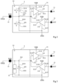
- FIG. 4 schematically represents an embodiment of an input-output circuit 7 of an electronic chip.
- the input/output circuit 7 of the figure 4 is, for example, yet another input-output circuit of chip 1.
- This input-output circuit 7 comprises common elements with the input-output circuit 5 of the picture 3 . These common elements will not be detailed again below.
- Terminal 17 is preferably on the chip core side (not shown in figure 4 ), which makes it possible not to modify the number of pads external to chip 1.
- a digital signal (or all-or-nothing signal), denoted CMD, is applied to terminal 17 of chip 1.
- the digital signal CMD therefore reaches switchable diode 71 via via its third pin 715.
- This digital signal CMD is suitable for controlling the switchable diode 71.
- circuit 7 is then comparable to circuit 3 ( figure 2 ), except that switchable diode 71 of circuit 7 provides an injection path to ground GND while diode 331 of circuit 3 provides an injection path to supply VDD.
- switchable diode 71 of circuit 7 provides an injection path to ground GND while diode 331 of circuit 3 provides an injection path to supply VDD.
- a second state, preferably a low state, of the control signal CMD makes it possible to form, between the first pin 711 and the second pin 713 of the switchable diode 71, an open circuit.
- circuit 7 When the CMD signal is in the low state, the circuit 7 is then comparable to the circuit 5 exposed in relation to the picture 3 . When the CMD signal is in the low state, we are therefore reduced to an operation of circuit 7 similar to that of circuit 5 ( picture 3 ).
- circuit 7 of chip 1 has the advantage of having a pad 15 that can be configured as a tolerant pad or as a non-tolerant pad, depending on the state of the digital signal CMD applied to terminal 17 of chip 1. This thus confers greater flexibility on circuit 7 and, more generally, on chip 1.
- FIG. 5 schematically represents an embodiment of a diode switchable by a digital signal.
- the transistors 73, 75 and 77 of the switchable diode 71 are preferably MOS type field effect transistors.
- the transistors 75 and 77 of the switchable diode 71 have, compared to the transistor 73, a different type of conductivity.
- Transistor 71 is preferably a P-type or P-channel MOS transistor (or P-channel MOSFET, PFET, PMOS, etc.) while transistors 75 and 77 are both transistors.
- N-type or N-channel MOS or N-channel MOSFET, NFET, NMOS, etc.
- the boxes (bulk) of transistors M2 and M3 are interconnected to source 771 of transistor M3 (ground GND).
- the well of transistor M1 is connected to source 731 of transistor M1 (pad 15).
- the first transistor 73 is theoretically on if a voltage less than or equal to the voltage VTH is applied between its gate 733 and its source 731.
- the first transistor 73 is theoretically off if a voltage strictly greater than the threshold voltage VTH is applied between its gate 733 and its source 731.
- the second transistor 75 is theoretically on if a voltage greater than or equal to the voltage VTH is applied between its gate 753 and its source 751.
- the second transistor 75 is theoretically off if a voltage strictly lower than the threshold voltage VTH is applied between its gate 753 and its source 751.
- Third transistor 77 is theoretically on if a voltage greater than or equal to voltage VTH is applied between its gate 773 and its source 771.
- the second transistor 77 is theoretically blocked if one applies, between its gate 773 and its source 771, a voltage strictly lower than the threshold voltage VTH.
- source 731 of first transistor 73 is connected to pad 15 of chip 1. Source 731 of first transistor 73 is therefore brought to voltage VPAD.
- Gate 773 of third transistor 77 is connected to terminal 17 of chip 1. Gate 773 of third transistor 77 is therefore controlled by digital signal CMD.
- switchable diode 71 When signal CMD is in the high state (case 5 and case 6), switchable diode 71 thus behaves like a diode characterized by a threshold voltage equal to VTH. When the CMD signal is in the low state (cases 1 to 4), the switchable diode 71 behaves, on the other hand, like an open circuit.
- the switchable diode 71 therefore has the advantage of preventing involuntary resupply, by applying a voltage to pad 15, chip 1 which is to be kept off.
Landscapes
- Engineering & Computer Science (AREA)
- Computer Hardware Design (AREA)
- Physics & Mathematics (AREA)
- Computing Systems (AREA)
- General Engineering & Computer Science (AREA)
- Mathematical Physics (AREA)
- Semiconductor Integrated Circuits (AREA)
- Amplifiers (AREA)
- Metal-Oxide And Bipolar Metal-Oxide Semiconductor Integrated Circuits (AREA)
Claims (9)
- Eingangs-Ausgangsschaltung (7) eines elektronischen Chips (1) mit einer Vorrichtung, die Folgendes aufweist:- einen Eingangsanschluss (11) eines Kerns (2) des Chips;- einen Ausgangsanschluss (13) des Kerns des Chips;- eine Ausgleichsschaltung (31) aufweisend eine erste Pufferschaltung (311), mit einem Ausgang (3111), der mit dem Eingangsanschluss verbunden ist, und eine zweite Pufferschaltung (313), mit einem Eingang (3133), der mit dem Ausgangsanschluss verbunden ist, wobei ein Eingang (3113) der ersten Pufferschaltung und ein Ausgang (3131) der zweiten Pufferschaltung über einen gemeinsamen Verbindungsknoten (315) miteinander verbunden sind, der mit einem Verbindungskontakt (15) des Chips verbunden ist; und- eine Schutzschaltung, die in Reihe (71) Folgendes aufweist:wobei das Gate (733) des ersten Transistors und das Gate (753) des zweiten Transistors miteinander verbunden sind und dazu bestimmt sind, eine Versorgungsspannung (VDD) des elektronischen Chips zu empfangen.einen ersten P-Typ-MOS-Transistor (73), dessen Source (731) mit dem Kontakt (15) verbunden ist;einen zweiten N-Typ-MOS-Transistor (75), der mit dem ersten Transistor verbunden ist; undeinen dritten N-Typ-MOS-Transistor (77), der mit dem zweiten Transistor verbunden ist, wobei der dritte Transistor (77) durch ein digitales Signal (CMD) gesteuert wird, das an einen Anschluss (17) des Chips angelegt wird,
- Schaltung nach Anspruch 1, wobei:- der Drain (755) des zweiten Transistors (75) mit dem Drain (735) des ersten Transistors (73) verbunden ist; und- die Source (751) des zweiten Transistors (75) mit dem Drain (775) des dritten Transistors (77) verbunden ist.
- Schaltung nach Anspruch 1 oder 2, wobei an die Source (771) des dritten Transistors (77) ein Referenzspannung (GND) angelegt ist.
- Schaltung nach einem der Ansprüche 1 bis 3, wobei die Versorgungsspannung (VDD) einer Gleichspannung entspricht, die zwischen den gemeinsamen Gates (733, 753) des ersten und zweiten Transistors (73, 75) und der Source (771) des dritten Transistors (77) angelegt ist.
- Schaltung nach einem der Ansprüche 1 bis 4, bei der das digitale Signal (CMD) geeignet ist, den Durchgang eines Stroms in der Reihenschaltung (71) in einer EIN-/-AUS Weise zu steuern.
- Schaltung nach einem der Ansprüche 1 bis 5, bei der die Reihenschaltung (71) in Abhängigkeit vom Zustand des digitalen Signals (CMD), das den dritten Transistor (77) steuert, manchmal eine Diode und manchmal einen offenen Stromkreis abbildet.
- Schaltung nach einem der Ansprüche 1 bis 6, wobei die Schaltung ferner Folgendes aufweist:- eine Diode (333) mit einer Anode (3331), die mit einem Knoten verbunden ist, an den eine Referenzspannung (GND) angelegt ist, und einer Kathode (3333), die mit der Source (731) des ersten Transistors (73) verbunden ist; und- ein Schutzbauteil (51) gegen vorübergehende Überspannungen, das parallel zu der Diode geschaltet ist.
- Elektronischer Chip (1) mit mindestens einer Schaltung (7) nach einem der Ansprüche 1 bis 7.
- Verfahren zur Steuerung einer Schaltung nach einem der Ansprüche 1 bis 7, wobei:- das digitale Steuersignal (CMD) in einen ersten Zustand versetzt wird, um eine Diodenfunktion zu bewirken; und- das digitale Steuersignal (CMD) in einen zweiten Zustand versetzt wird, um einen offenen Stromkreis zu erzwingen.
Applications Claiming Priority (1)
| Application Number | Priority Date | Filing Date | Title |
|---|---|---|---|
| FR1904484A FR3095560B1 (fr) | 2019-04-26 | 2019-04-26 | Association de transistors en série |
Publications (2)
| Publication Number | Publication Date |
|---|---|
| EP3731414A1 EP3731414A1 (de) | 2020-10-28 |
| EP3731414B1 true EP3731414B1 (de) | 2023-03-15 |
Family
ID=67514917
Family Applications (1)
| Application Number | Title | Priority Date | Filing Date |
|---|---|---|---|
| EP20171008.4A Active EP3731414B1 (de) | 2019-04-26 | 2020-04-23 | Eingangs-ausgangsschaltung umfassend eine schutzschaltung mit einer reihenschaltung von transistoren, und verfahren zum steuern der schaltung |
Country Status (4)
| Country | Link |
|---|---|
| US (2) | US11133798B2 (de) |
| EP (1) | EP3731414B1 (de) |
| CN (2) | CN111865293B (de) |
| FR (1) | FR3095560B1 (de) |
Families Citing this family (3)
| Publication number | Priority date | Publication date | Assignee | Title |
|---|---|---|---|---|
| FR3095560B1 (fr) * | 2019-04-26 | 2021-12-03 | St Microelectronics Rousset | Association de transistors en série |
| US12183731B2 (en) * | 2021-01-18 | 2024-12-31 | Taiwan Semiconductor Manufacturing Company Ltd. | Dummy device for core device to operate in a safe operating area and method for manufacturing the same |
| US11716073B2 (en) | 2021-04-07 | 2023-08-01 | Mediatek Inc. | Chip with pad tracking |
Family Cites Families (12)
| Publication number | Priority date | Publication date | Assignee | Title |
|---|---|---|---|---|
| JPH0748652B2 (ja) * | 1987-07-23 | 1995-05-24 | 三菱電機株式会社 | 半導体回路装置の入力保護装置 |
| US5118968A (en) * | 1990-09-12 | 1992-06-02 | Micron Technology, Inc. | Special mode activation circuit for selectively activating a special mode circuit of a semiconductor integrated circuit device |
| US5723990A (en) * | 1995-06-21 | 1998-03-03 | Micron Quantum Devices, Inc. | Integrated circuit having high voltage detection circuit |
| US5745323A (en) * | 1995-06-30 | 1998-04-28 | Analog Devices, Inc. | Electrostatic discharge protection circuit for protecting CMOS transistors on integrated circuit processes |
| JP3258229B2 (ja) * | 1996-03-18 | 2002-02-18 | 株式会社東芝 | レベル変換回路及び半導体集積回路 |
| JP3701942B2 (ja) * | 2003-01-21 | 2005-10-05 | 沖電気工業株式会社 | レベル変換回路 |
| WO2005018091A1 (ja) * | 2003-08-13 | 2005-02-24 | Fujitsu Limited | パルス生成回路 |
| FR2957732A1 (fr) * | 2010-03-16 | 2011-09-23 | St Microelectronics Crolles 2 | Etage de sortie d'un circuit electronique |
| JP6065737B2 (ja) * | 2013-05-10 | 2017-01-25 | 株式会社ソシオネクスト | 出力回路および電圧信号出力方法 |
| ITUA20162889A1 (it) * | 2016-04-26 | 2017-10-26 | St Microelectronics Srl | Circuito di commutazione, relativo procedimento e circuito integrato |
| US10355672B2 (en) * | 2017-06-29 | 2019-07-16 | SK Hynix Inc. | Semiconductor device with power gating scheme |
| FR3095560B1 (fr) * | 2019-04-26 | 2021-12-03 | St Microelectronics Rousset | Association de transistors en série |
-
2019
- 2019-04-26 FR FR1904484A patent/FR3095560B1/fr active Active
-
2020
- 2020-04-23 US US16/856,448 patent/US11133798B2/en active Active
- 2020-04-23 EP EP20171008.4A patent/EP3731414B1/de active Active
- 2020-04-24 CN CN202010334227.5A patent/CN111865293B/zh active Active
- 2020-04-24 CN CN202020637485.6U patent/CN211830743U/zh active Active
-
2021
- 2021-08-25 US US17/411,838 patent/US11509305B2/en active Active
Also Published As
| Publication number | Publication date |
|---|---|
| FR3095560A1 (fr) | 2020-10-30 |
| US11509305B2 (en) | 2022-11-22 |
| FR3095560B1 (fr) | 2021-12-03 |
| CN111865293A (zh) | 2020-10-30 |
| US11133798B2 (en) | 2021-09-28 |
| EP3731414A1 (de) | 2020-10-28 |
| CN111865293B (zh) | 2025-06-24 |
| US20200343890A1 (en) | 2020-10-29 |
| US20210384903A1 (en) | 2021-12-09 |
| CN211830743U (zh) | 2020-10-30 |
Similar Documents
| Publication | Publication Date | Title |
|---|---|---|
| EP3731414B1 (de) | Eingangs-ausgangsschaltung umfassend eine schutzschaltung mit einer reihenschaltung von transistoren, und verfahren zum steuern der schaltung | |
| EP0594834B1 (de) | In Standard-CMOS-Technologie realisierte, zwischen einer Logikschaltung mit niedriger Versorgungsspannung und einer Ausgangsstufe mit hoher Versorgungsspannung, liegende Schaltung | |
| WO2011089179A1 (fr) | Dispositif electronique, en particulier de protection contre les décharges électrostatistiques, et procédé de protection d'un composant contre des décharges électrostatiques | |
| US6072219A (en) | Substrate-triggering electrostatic discharge protection circuit for deep-submicron integrated circuits | |
| US8300370B2 (en) | ESD protection circuit and circuitry of IC applying the ESD protection circuit | |
| CN107195645B (zh) | 摄像装置 | |
| FR2812972A1 (fr) | Dispositif a semiconducteur consistant en un thyristor pour la protection contre les decharges electrostatiques | |
| WO2017203187A1 (fr) | Circuit intégré comprenant une pluralité de puces formées d'un transistor à haute tension et comprenant une puce formée d'un transistor à basse tension | |
| EP2290691A1 (de) | Schutzvorrichtung für einen integrierten Schaltkreis gegen elektrostatische Entladungen | |
| EP2280414B1 (de) | Elektronische Vorrichtung zum Schutz gegen Sperrspannung und ihre Anwendung im Automobilbereich | |
| FR2982416A1 (fr) | Dispositif electronique de protection contre les decharges electrostatiques | |
| FR3016999A1 (fr) | Dispositif electronique, en particulier pour la protection contre les decharges electrostatiques | |
| EP0543745A1 (de) | MOS-Transistor mit integrierter Zener-Schutzdiode | |
| FR3106941A1 (fr) | Protection contre des surtensions | |
| EP2348528A1 (de) | Schutzvorrichtung für einen integrierten Schaltkreis gegen elektrostatische Entladungen | |
| FR3131981A1 (fr) | Dispositif de protection contre les décharges électrostatiques | |
| EP0697734B1 (de) | Schutzschaltung gegen elektrostatische Entladung | |
| EP1309005B1 (de) | Schutz einer integrierten Schaltung gegen ESD und andere Überspannungen | |
| EP3370256B1 (de) | Kompakte vorrichtung zum schutz eines integrierten schaltkreises gegen elektrostatische entladungen | |
| EP2246886A1 (de) | Integrierter Schaltkreis, der mit einem großflächigen Schutz gegen elektrostatische Entladungen ausgestattet ist | |
| EP0895331A1 (de) | Schutzvorrichtung für elektrische Last und Versorgungseinrichtung mit einer solchen Vorrichtung | |
| EP1638146A2 (de) | Elektronische Schaltung mit zweifacher Speisespannung und mit Schutzeinrichtung gegen Überschläge, und entsprechende Schutzeinrichtung | |
| FR2993402A1 (fr) | Circuit integre sur soi comprenant une diode laterale de protection contre des decharges electrostatiques | |
| FR3119493A1 (fr) | Dispositif de protection contre les décharges électrostatiques | |
| EP0820135A1 (de) | Statischer selbsthaltender Mikroschalter |
Legal Events
| Date | Code | Title | Description |
|---|---|---|---|
| PUAI | Public reference made under article 153(3) epc to a published international application that has entered the european phase |
Free format text: ORIGINAL CODE: 0009012 |
|
| STAA | Information on the status of an ep patent application or granted ep patent |
Free format text: STATUS: REQUEST FOR EXAMINATION WAS MADE |
|
| 17P | Request for examination filed |
Effective date: 20200423 |
|
| AK | Designated contracting states |
Kind code of ref document: A1 Designated state(s): AL AT BE BG CH CY CZ DE DK EE ES FI FR GB GR HR HU IE IS IT LI LT LU LV MC MK MT NL NO PL PT RO RS SE SI SK SM TR |
|
| AX | Request for extension of the european patent |
Extension state: BA ME |
|
| STAA | Information on the status of an ep patent application or granted ep patent |
Free format text: STATUS: EXAMINATION IS IN PROGRESS |
|
| 17Q | First examination report despatched |
Effective date: 20210510 |
|
| GRAP | Despatch of communication of intention to grant a patent |
Free format text: ORIGINAL CODE: EPIDOSNIGR1 |
|
| STAA | Information on the status of an ep patent application or granted ep patent |
Free format text: STATUS: GRANT OF PATENT IS INTENDED |
|
| INTG | Intention to grant announced |
Effective date: 20221013 |
|
| GRAS | Grant fee paid |
Free format text: ORIGINAL CODE: EPIDOSNIGR3 |
|
| GRAA | (expected) grant |
Free format text: ORIGINAL CODE: 0009210 |
|
| STAA | Information on the status of an ep patent application or granted ep patent |
Free format text: STATUS: THE PATENT HAS BEEN GRANTED |
|
| AK | Designated contracting states |
Kind code of ref document: B1 Designated state(s): AL AT BE BG CH CY CZ DE DK EE ES FI FR GB GR HR HU IE IS IT LI LT LU LV MC MK MT NL NO PL PT RO RS SE SI SK SM TR |
|
| REG | Reference to a national code |
Ref country code: CH Ref legal event code: EP Ref country code: GB Ref legal event code: FG4D Free format text: NOT ENGLISH |
|
| REG | Reference to a national code |
Ref country code: DE Ref legal event code: R096 Ref document number: 602020008802 Country of ref document: DE |
|
| REG | Reference to a national code |
Ref country code: IE Ref legal event code: FG4D Free format text: LANGUAGE OF EP DOCUMENT: FRENCH |
|
| REG | Reference to a national code |
Ref country code: AT Ref legal event code: REF Ref document number: 1554570 Country of ref document: AT Kind code of ref document: T Effective date: 20230415 |
|
| REG | Reference to a national code |
Ref country code: LT Ref legal event code: MG9D |
|
| REG | Reference to a national code |
Ref country code: NL Ref legal event code: MP Effective date: 20230315 |
|
| PG25 | Lapsed in a contracting state [announced via postgrant information from national office to epo] |
Ref country code: RS Free format text: LAPSE BECAUSE OF FAILURE TO SUBMIT A TRANSLATION OF THE DESCRIPTION OR TO PAY THE FEE WITHIN THE PRESCRIBED TIME-LIMIT Effective date: 20230315 Ref country code: NO Free format text: LAPSE BECAUSE OF FAILURE TO SUBMIT A TRANSLATION OF THE DESCRIPTION OR TO PAY THE FEE WITHIN THE PRESCRIBED TIME-LIMIT Effective date: 20230615 Ref country code: LV Free format text: LAPSE BECAUSE OF FAILURE TO SUBMIT A TRANSLATION OF THE DESCRIPTION OR TO PAY THE FEE WITHIN THE PRESCRIBED TIME-LIMIT Effective date: 20230315 Ref country code: LT Free format text: LAPSE BECAUSE OF FAILURE TO SUBMIT A TRANSLATION OF THE DESCRIPTION OR TO PAY THE FEE WITHIN THE PRESCRIBED TIME-LIMIT Effective date: 20230315 Ref country code: HR Free format text: LAPSE BECAUSE OF FAILURE TO SUBMIT A TRANSLATION OF THE DESCRIPTION OR TO PAY THE FEE WITHIN THE PRESCRIBED TIME-LIMIT Effective date: 20230315 |
|
| REG | Reference to a national code |
Ref country code: AT Ref legal event code: MK05 Ref document number: 1554570 Country of ref document: AT Kind code of ref document: T Effective date: 20230315 |
|
| PG25 | Lapsed in a contracting state [announced via postgrant information from national office to epo] |
Ref country code: SE Free format text: LAPSE BECAUSE OF FAILURE TO SUBMIT A TRANSLATION OF THE DESCRIPTION OR TO PAY THE FEE WITHIN THE PRESCRIBED TIME-LIMIT Effective date: 20230315 Ref country code: NL Free format text: LAPSE BECAUSE OF FAILURE TO SUBMIT A TRANSLATION OF THE DESCRIPTION OR TO PAY THE FEE WITHIN THE PRESCRIBED TIME-LIMIT Effective date: 20230315 Ref country code: GR Free format text: LAPSE BECAUSE OF FAILURE TO SUBMIT A TRANSLATION OF THE DESCRIPTION OR TO PAY THE FEE WITHIN THE PRESCRIBED TIME-LIMIT Effective date: 20230616 Ref country code: FI Free format text: LAPSE BECAUSE OF FAILURE TO SUBMIT A TRANSLATION OF THE DESCRIPTION OR TO PAY THE FEE WITHIN THE PRESCRIBED TIME-LIMIT Effective date: 20230315 |
|
| PG25 | Lapsed in a contracting state [announced via postgrant information from national office to epo] |
Ref country code: SM Free format text: LAPSE BECAUSE OF FAILURE TO SUBMIT A TRANSLATION OF THE DESCRIPTION OR TO PAY THE FEE WITHIN THE PRESCRIBED TIME-LIMIT Effective date: 20230315 Ref country code: RO Free format text: LAPSE BECAUSE OF FAILURE TO SUBMIT A TRANSLATION OF THE DESCRIPTION OR TO PAY THE FEE WITHIN THE PRESCRIBED TIME-LIMIT Effective date: 20230315 Ref country code: PT Free format text: LAPSE BECAUSE OF FAILURE TO SUBMIT A TRANSLATION OF THE DESCRIPTION OR TO PAY THE FEE WITHIN THE PRESCRIBED TIME-LIMIT Effective date: 20230717 Ref country code: ES Free format text: LAPSE BECAUSE OF FAILURE TO SUBMIT A TRANSLATION OF THE DESCRIPTION OR TO PAY THE FEE WITHIN THE PRESCRIBED TIME-LIMIT Effective date: 20230315 Ref country code: EE Free format text: LAPSE BECAUSE OF FAILURE TO SUBMIT A TRANSLATION OF THE DESCRIPTION OR TO PAY THE FEE WITHIN THE PRESCRIBED TIME-LIMIT Effective date: 20230315 Ref country code: CZ Free format text: LAPSE BECAUSE OF FAILURE TO SUBMIT A TRANSLATION OF THE DESCRIPTION OR TO PAY THE FEE WITHIN THE PRESCRIBED TIME-LIMIT Effective date: 20230315 Ref country code: AT Free format text: LAPSE BECAUSE OF FAILURE TO SUBMIT A TRANSLATION OF THE DESCRIPTION OR TO PAY THE FEE WITHIN THE PRESCRIBED TIME-LIMIT Effective date: 20230315 |
|
| PG25 | Lapsed in a contracting state [announced via postgrant information from national office to epo] |
Ref country code: SK Free format text: LAPSE BECAUSE OF FAILURE TO SUBMIT A TRANSLATION OF THE DESCRIPTION OR TO PAY THE FEE WITHIN THE PRESCRIBED TIME-LIMIT Effective date: 20230315 Ref country code: PL Free format text: LAPSE BECAUSE OF FAILURE TO SUBMIT A TRANSLATION OF THE DESCRIPTION OR TO PAY THE FEE WITHIN THE PRESCRIBED TIME-LIMIT Effective date: 20230315 Ref country code: IS Free format text: LAPSE BECAUSE OF FAILURE TO SUBMIT A TRANSLATION OF THE DESCRIPTION OR TO PAY THE FEE WITHIN THE PRESCRIBED TIME-LIMIT Effective date: 20230715 |
|
| REG | Reference to a national code |
Ref country code: CH Ref legal event code: PL |
|
| REG | Reference to a national code |
Ref country code: DE Ref legal event code: R097 Ref document number: 602020008802 Country of ref document: DE |
|
| PG25 | Lapsed in a contracting state [announced via postgrant information from national office to epo] |
Ref country code: LU Free format text: LAPSE BECAUSE OF NON-PAYMENT OF DUE FEES Effective date: 20230423 |
|
| REG | Reference to a national code |
Ref country code: BE Ref legal event code: MM Effective date: 20230430 |
|
| PG25 | Lapsed in a contracting state [announced via postgrant information from national office to epo] |
Ref country code: MC Free format text: LAPSE BECAUSE OF FAILURE TO SUBMIT A TRANSLATION OF THE DESCRIPTION OR TO PAY THE FEE WITHIN THE PRESCRIBED TIME-LIMIT Effective date: 20230315 |
|
| PLBE | No opposition filed within time limit |
Free format text: ORIGINAL CODE: 0009261 |
|
| STAA | Information on the status of an ep patent application or granted ep patent |
Free format text: STATUS: NO OPPOSITION FILED WITHIN TIME LIMIT |
|
| PG25 | Lapsed in a contracting state [announced via postgrant information from national office to epo] |
Ref country code: SI Free format text: LAPSE BECAUSE OF FAILURE TO SUBMIT A TRANSLATION OF THE DESCRIPTION OR TO PAY THE FEE WITHIN THE PRESCRIBED TIME-LIMIT Effective date: 20230315 Ref country code: MC Free format text: LAPSE BECAUSE OF FAILURE TO SUBMIT A TRANSLATION OF THE DESCRIPTION OR TO PAY THE FEE WITHIN THE PRESCRIBED TIME-LIMIT Effective date: 20230315 Ref country code: LI Free format text: LAPSE BECAUSE OF NON-PAYMENT OF DUE FEES Effective date: 20230430 Ref country code: DK Free format text: LAPSE BECAUSE OF FAILURE TO SUBMIT A TRANSLATION OF THE DESCRIPTION OR TO PAY THE FEE WITHIN THE PRESCRIBED TIME-LIMIT Effective date: 20230315 Ref country code: CH Free format text: LAPSE BECAUSE OF NON-PAYMENT OF DUE FEES Effective date: 20230430 |
|
| REG | Reference to a national code |
Ref country code: IE Ref legal event code: MM4A |
|
| 26N | No opposition filed |
Effective date: 20231218 |
|
| PG25 | Lapsed in a contracting state [announced via postgrant information from national office to epo] |
Ref country code: BE Free format text: LAPSE BECAUSE OF NON-PAYMENT OF DUE FEES Effective date: 20230430 |
|
| PG25 | Lapsed in a contracting state [announced via postgrant information from national office to epo] |
Ref country code: IE Free format text: LAPSE BECAUSE OF NON-PAYMENT OF DUE FEES Effective date: 20230423 |
|
| PG25 | Lapsed in a contracting state [announced via postgrant information from national office to epo] |
Ref country code: IE Free format text: LAPSE BECAUSE OF NON-PAYMENT OF DUE FEES Effective date: 20230423 |
|
| PG25 | Lapsed in a contracting state [announced via postgrant information from national office to epo] |
Ref country code: IT Free format text: LAPSE BECAUSE OF FAILURE TO SUBMIT A TRANSLATION OF THE DESCRIPTION OR TO PAY THE FEE WITHIN THE PRESCRIBED TIME-LIMIT Effective date: 20230315 Ref country code: FR Free format text: LAPSE BECAUSE OF NON-PAYMENT OF DUE FEES Effective date: 20230515 |
|
| PG25 | Lapsed in a contracting state [announced via postgrant information from national office to epo] |
Ref country code: BG Free format text: LAPSE BECAUSE OF FAILURE TO SUBMIT A TRANSLATION OF THE DESCRIPTION OR TO PAY THE FEE WITHIN THE PRESCRIBED TIME-LIMIT Effective date: 20230315 |
|
| PG25 | Lapsed in a contracting state [announced via postgrant information from national office to epo] |
Ref country code: BG Free format text: LAPSE BECAUSE OF FAILURE TO SUBMIT A TRANSLATION OF THE DESCRIPTION OR TO PAY THE FEE WITHIN THE PRESCRIBED TIME-LIMIT Effective date: 20230315 |
|
| GBPC | Gb: european patent ceased through non-payment of renewal fee |
Effective date: 20240423 |
|
| PG25 | Lapsed in a contracting state [announced via postgrant information from national office to epo] |
Ref country code: GB Free format text: LAPSE BECAUSE OF NON-PAYMENT OF DUE FEES Effective date: 20240423 |
|
| PG25 | Lapsed in a contracting state [announced via postgrant information from national office to epo] |
Ref country code: GB Free format text: LAPSE BECAUSE OF NON-PAYMENT OF DUE FEES Effective date: 20240423 |
|
| PGFP | Annual fee paid to national office [announced via postgrant information from national office to epo] |
Ref country code: DE Payment date: 20250319 Year of fee payment: 6 |
|
| PG25 | Lapsed in a contracting state [announced via postgrant information from national office to epo] |
Ref country code: CY Free format text: LAPSE BECAUSE OF FAILURE TO SUBMIT A TRANSLATION OF THE DESCRIPTION OR TO PAY THE FEE WITHIN THE PRESCRIBED TIME-LIMIT; INVALID AB INITIO Effective date: 20200423 |
|
| PG25 | Lapsed in a contracting state [announced via postgrant information from national office to epo] |
Ref country code: HU Free format text: LAPSE BECAUSE OF FAILURE TO SUBMIT A TRANSLATION OF THE DESCRIPTION OR TO PAY THE FEE WITHIN THE PRESCRIBED TIME-LIMIT; INVALID AB INITIO Effective date: 20200423 |
|
| PG25 | Lapsed in a contracting state [announced via postgrant information from national office to epo] |
Ref country code: TR Free format text: LAPSE BECAUSE OF FAILURE TO SUBMIT A TRANSLATION OF THE DESCRIPTION OR TO PAY THE FEE WITHIN THE PRESCRIBED TIME-LIMIT Effective date: 20230315 |