EP3379592B1 - Umwandlungsvorrichtung mit perowskitverbindung, verfahren zur herstellung davon und bildgebungsvorrichtung damit - Google Patents
Umwandlungsvorrichtung mit perowskitverbindung, verfahren zur herstellung davon und bildgebungsvorrichtung damit Download PDFInfo
- Publication number
- EP3379592B1 EP3379592B1 EP18161006.4A EP18161006A EP3379592B1 EP 3379592 B1 EP3379592 B1 EP 3379592B1 EP 18161006 A EP18161006 A EP 18161006A EP 3379592 B1 EP3379592 B1 EP 3379592B1
- Authority
- EP
- European Patent Office
- Prior art keywords
- photoelectric conversion
- formula
- blocking layer
- perovskite compound
- layer
- Prior art date
- Legal status (The legal status is an assumption and is not a legal conclusion. Google has not performed a legal analysis and makes no representation as to the accuracy of the status listed.)
- Active
Links
Images


Classifications
-
- H—ELECTRICITY
- H10—SEMICONDUCTOR DEVICES; ELECTRIC SOLID-STATE DEVICES NOT OTHERWISE PROVIDED FOR
- H10K—ORGANIC ELECTRIC SOLID-STATE DEVICES
- H10K50/00—Organic light-emitting devices
- H10K50/10—OLEDs or polymer light-emitting diodes [PLED]
- H10K50/14—Carrier transporting layers
-
- H—ELECTRICITY
- H10—SEMICONDUCTOR DEVICES; ELECTRIC SOLID-STATE DEVICES NOT OTHERWISE PROVIDED FOR
- H10F—INORGANIC SEMICONDUCTOR DEVICES SENSITIVE TO INFRARED RADIATION, LIGHT, ELECTROMAGNETIC RADIATION OF SHORTER WAVELENGTH OR CORPUSCULAR RADIATION
- H10F39/00—Integrated devices, or assemblies of multiple devices, comprising at least one element covered by group H10F30/00, e.g. radiation detectors comprising photodiode arrays
- H10F39/011—Manufacture or treatment of image sensors covered by group H10F39/12
- H10F39/024—Manufacture or treatment of image sensors covered by group H10F39/12 of coatings or optical elements
-
- H—ELECTRICITY
- H10—SEMICONDUCTOR DEVICES; ELECTRIC SOLID-STATE DEVICES NOT OTHERWISE PROVIDED FOR
- H10F—INORGANIC SEMICONDUCTOR DEVICES SENSITIVE TO INFRARED RADIATION, LIGHT, ELECTROMAGNETIC RADIATION OF SHORTER WAVELENGTH OR CORPUSCULAR RADIATION
- H10F19/00—Integrated devices, or assemblies of multiple devices, comprising at least one photovoltaic cell covered by group H10F10/00, e.g. photovoltaic modules
- H10F19/30—Integrated devices, or assemblies of multiple devices, comprising at least one photovoltaic cell covered by group H10F10/00, e.g. photovoltaic modules comprising thin-film photovoltaic cells
- H10F19/31—Integrated devices, or assemblies of multiple devices, comprising at least one photovoltaic cell covered by group H10F10/00, e.g. photovoltaic modules comprising thin-film photovoltaic cells having multiple laterally adjacent thin-film photovoltaic cells deposited on the same substrate
- H10F19/33—Patterning processes to connect the photovoltaic cells, e.g. laser cutting of conductive or active layers
-
- H—ELECTRICITY
- H10—SEMICONDUCTOR DEVICES; ELECTRIC SOLID-STATE DEVICES NOT OTHERWISE PROVIDED FOR
- H10F—INORGANIC SEMICONDUCTOR DEVICES SENSITIVE TO INFRARED RADIATION, LIGHT, ELECTROMAGNETIC RADIATION OF SHORTER WAVELENGTH OR CORPUSCULAR RADIATION
- H10F19/00—Integrated devices, or assemblies of multiple devices, comprising at least one photovoltaic cell covered by group H10F10/00, e.g. photovoltaic modules
- H10F19/50—Integrated devices comprising at least one photovoltaic cell and other types of semiconductor or solid-state components
-
- H—ELECTRICITY
- H10—SEMICONDUCTOR DEVICES; ELECTRIC SOLID-STATE DEVICES NOT OTHERWISE PROVIDED FOR
- H10F—INORGANIC SEMICONDUCTOR DEVICES SENSITIVE TO INFRARED RADIATION, LIGHT, ELECTROMAGNETIC RADIATION OF SHORTER WAVELENGTH OR CORPUSCULAR RADIATION
- H10F71/00—Manufacture or treatment of devices covered by this subclass
-
- H—ELECTRICITY
- H10—SEMICONDUCTOR DEVICES; ELECTRIC SOLID-STATE DEVICES NOT OTHERWISE PROVIDED FOR
- H10K—ORGANIC ELECTRIC SOLID-STATE DEVICES
- H10K30/00—Organic devices sensitive to infrared radiation, light, electromagnetic radiation of shorter wavelength or corpuscular radiation
- H10K30/20—Organic devices sensitive to infrared radiation, light, electromagnetic radiation of shorter wavelength or corpuscular radiation comprising organic-organic junctions, e.g. donor-acceptor junctions
- H10K30/211—Organic devices sensitive to infrared radiation, light, electromagnetic radiation of shorter wavelength or corpuscular radiation comprising organic-organic junctions, e.g. donor-acceptor junctions comprising multiple junctions, e.g. double heterojunctions
-
- H—ELECTRICITY
- H10—SEMICONDUCTOR DEVICES; ELECTRIC SOLID-STATE DEVICES NOT OTHERWISE PROVIDED FOR
- H10K—ORGANIC ELECTRIC SOLID-STATE DEVICES
- H10K30/00—Organic devices sensitive to infrared radiation, light, electromagnetic radiation of shorter wavelength or corpuscular radiation
- H10K30/50—Photovoltaic [PV] devices
-
- H—ELECTRICITY
- H10—SEMICONDUCTOR DEVICES; ELECTRIC SOLID-STATE DEVICES NOT OTHERWISE PROVIDED FOR
- H10K—ORGANIC ELECTRIC SOLID-STATE DEVICES
- H10K85/00—Organic materials used in the body or electrodes of devices covered by this subclass
- H10K85/50—Organic perovskites; Hybrid organic-inorganic perovskites [HOIP], e.g. CH3NH3PbI3
-
- H—ELECTRICITY
- H10—SEMICONDUCTOR DEVICES; ELECTRIC SOLID-STATE DEVICES NOT OTHERWISE PROVIDED FOR
- H10K—ORGANIC ELECTRIC SOLID-STATE DEVICES
- H10K71/00—Manufacture or treatment specially adapted for the organic devices covered by this subclass
-
- H—ELECTRICITY
- H10—SEMICONDUCTOR DEVICES; ELECTRIC SOLID-STATE DEVICES NOT OTHERWISE PROVIDED FOR
- H10K—ORGANIC ELECTRIC SOLID-STATE DEVICES
- H10K71/00—Manufacture or treatment specially adapted for the organic devices covered by this subclass
- H10K71/10—Deposition of organic active material
- H10K71/12—Deposition of organic active material using liquid deposition, e.g. spin coating
-
- Y—GENERAL TAGGING OF NEW TECHNOLOGICAL DEVELOPMENTS; GENERAL TAGGING OF CROSS-SECTIONAL TECHNOLOGIES SPANNING OVER SEVERAL SECTIONS OF THE IPC; TECHNICAL SUBJECTS COVERED BY FORMER USPC CROSS-REFERENCE ART COLLECTIONS [XRACs] AND DIGESTS
- Y02—TECHNOLOGIES OR APPLICATIONS FOR MITIGATION OR ADAPTATION AGAINST CLIMATE CHANGE
- Y02E—REDUCTION OF GREENHOUSE GAS [GHG] EMISSIONS, RELATED TO ENERGY GENERATION, TRANSMISSION OR DISTRIBUTION
- Y02E10/00—Energy generation through renewable energy sources
- Y02E10/50—Photovoltaic [PV] energy
- Y02E10/549—Organic PV cells
-
- Y—GENERAL TAGGING OF NEW TECHNOLOGICAL DEVELOPMENTS; GENERAL TAGGING OF CROSS-SECTIONAL TECHNOLOGIES SPANNING OVER SEVERAL SECTIONS OF THE IPC; TECHNICAL SUBJECTS COVERED BY FORMER USPC CROSS-REFERENCE ART COLLECTIONS [XRACs] AND DIGESTS
- Y02—TECHNOLOGIES OR APPLICATIONS FOR MITIGATION OR ADAPTATION AGAINST CLIMATE CHANGE
- Y02P—CLIMATE CHANGE MITIGATION TECHNOLOGIES IN THE PRODUCTION OR PROCESSING OF GOODS
- Y02P70/00—Climate change mitigation technologies in the production process for final industrial or consumer products
- Y02P70/50—Manufacturing or production processes characterised by the final manufactured product
Definitions
- the present disclosure relates to a photoelectric conversion device including a perovskite compound, method of manufacturing the same and an imaging device including the same.
- a photoelectric conversion device refers to a device which converts an optical signal to an electrical signal.
- a photoelectric conversion device uses photoelectric effects, for example, a photoconductive effect and a photovoltaic effect for converting an optical signal to an electrical signal.
- such a photoelectric conversion device may be used in an imaging device.
- the imaging device may include photoelectric conversion devices arranged two-dimensionally on transistors, and collect electrical signals generated from the photoelectric conversion devices.
- EP 2 942 826 A2 relates to doped perovskites and their use as active and/or charge transport layers in optoelectronic devices and the manufacturing of an optoelectronic device.
- WO 2016/115602 A1 discloses a process of forming a photoactive layer of a planar perovskite photoactive device.
- a photoelectric conversion device including a perovskite compound and an imaging device including the same, and more particularly, a photoelectric conversion device including a perovskite compound in an electron blocking layer and a hole blocking layer, and an imaging device including the photoelectric conversion device.
- An aspect of the invention provides a photoelectric conversion device in accordance with claim 1.
- Another aspect of the invention provides a method of manufacturing a photoelectric conversion device in accordance with claim 12.
- Another aspect of the invention provides an imaging device in accordance with claim 15.
- perovskite compound refers to a compound represented by, for example, the formula of ABX 3 , wherein A and B are cations having different sizes, and X is an anion.
- a site of the cation A may be at (0,0,0)
- a site of the cation B may be at (1/2,1/2,1/2)
- a site of the anion X may be at (1/2,1/2,0).
- the perovskite compound may have a twisted structure with lower symmetry, compared to the ideal symmetric structure of calcium titanium oxide (CaTiOs), depending on types of A, B, and X. It will be understood that the perovskite compound used herein may encompass a compound having the ideal symmetric structure and a compound having a twisted structure with low symmetry.
- FIG. 1 is a schematic cross-sectional side view of a photoelectric conversion device 100 according to an embodiment.
- the photoelectric conversion device 100 includes a first conductive layer 110, a second conductive layer 150, an electron blocking layer 120, a photoelectric conversion layer 130, and a hole blocking layer 140.
- the electron blocking layer 120, the photoelectric conversion layer 130 and the hole blocking layer 140 are between the first conductive layer 110 and the second conductive layer 150.
- the electron blocking layer 120 is between the first conductive layer 110 and the photoelectric conversion layer 130.
- the hole blocking layer 140 is between the second conductive layer 150 and the photoelectric conversion layer 130.
- the electron blocking layer 120 includes a first perovskite compound represented by Formula 1.
- a 1 is at least one monovalent organic cation, at least one monovalent inorganic cation, or any combination thereof.
- a 1 may be i) a monovalent organic cation, ii) a monovalent inorganic cation, iii) at least two different monovalent organic cations, iv) at least two different monovalent inorganic cations, or v) any combination of at least one monovalent organic cation and at least one monovalent inorganic cation.
- example embodiments are not limited thereto.
- a 1 may be (CH 3 NH 3 ) + , ((CH 3 ) 2 PH 2 ) + , (CH 3 ASH 3 ) + , (NH 4 ) + , (CH 3 SbH 3 ) + , (PH 4 ) + , , (PF 4 ) + , (CH 3 PH 3 ) + , (C 7 H 7 ) + , (SbH 4 ) + , (AsH 4 ) + , (NCl 4 ) + , (NH 3 OH) + , (NH 3 NH 2 ) + , (CH(NH 2 ) 2 ) + , (C 3 N 2 H 5 ) + , ((CH 3 ) 2 NH 2 ) + , (NC 4 H 8 ) + , ((CH 3 CH 2 )NH 3 ) + , ((NH 2 ) 3 C) + , ((CH 3 CH 2 CH 2 CH 2 )NH 3 ) + , (CH 3 ASH 3 ) +
- a 1 may be (CH 3 NH 3 ) + , ((CH 3 CH 2 CH 2 CH 2 )NH 3 ) + , (NH 2 CHNH 2 ) + , K + , Rb + , Cs + , or any combination thereof.
- example embodiments are not limited thereto.
- B 1 is at least one divalent inorganic cation.
- B 1 may be i) a divalent inorganic cation, or ii) a combination of at least two different divalent inorganic cations.
- example embodiments are not limited thereto.
- B 1 may be a divalent cation of a rare earth metal, a divalent cation of an alkali earth metal, a divalent cation of a transition metal, a divalent cation of a late transition metal, or any combination thereof.
- example embodiments are not limited thereto.
- B 1 may be La 2+ , Ce 2+ , Pr 2+ , Nd 2+ , Pm 2+ , Sm 2+ , Eu 2+ , Gd 2+ , Tb 2+ , Dy 2+ , Ho 2+ , Er 2+ , Tm 2+ , Yb 2+ , Lu 2+ , Be 2+ , Mg 2+ , Ca 2+ , Sr 2+ , Ba 2+ , Ra 2+ , Pb 2+ , Sn 2+ , or any combination thereof.
- example embodiments are not limited thereto.
- B 1 may be Pb 2+ , Sn 2+ , or any combination thereof. However, example embodiments are not limited thereto.
- B 1 may be Pb 2+ .
- example embodiments are not limited thereto.
- X 1 and Y 1 are each independently at least one monovalent anion, wherein X 1 and Y 1 are the same as or different from each other.
- X 1 and Y 1 may each independently be i) a monovalent anion, or ii) any combination of at least two different monovalent anions.
- example embodiments are not limited thereto.
- X 1 and Y 1 may each independently be at least one halide anion.
- example embodiments are not limited thereto.
- X 1 and Y 1 may each independently be selected from Cl - , Br, and I - .
- example embodiments are not limited thereto.
- n is a real number satisfying 0 ⁇ n ⁇ 3.
- n may be a real number satisfying 0 ⁇ n ⁇ 3.
- example embodiments are not limited thereto.
- the hole blocking layer 140 includes a second perovskite compound represented by Formula 2.
- a 2 is the same as A 1 in Formula 1 as described above
- B 2 is the same as B 1 in Formula 1 as described above
- X 2 is the same as X 1 in Formula 1 as described above
- Y 2 is the same as Y 1 in Formula 1 as described above
- m is the same as n in Formula 1 as described above.
- the first perovskite compound represented by Formula 1 and the second perovskite compound represented by Formula 2 may each independently be selected from CH 3 NH 3 PbI 3 , CH 3 NH 3 PbBr 3 , CH 3 NH 3 PbBr (3-o) I o , CH 3 NH 3 PbCl (3-o) Br o , CH 3 NH 3 PbCl (3-o) I o , CsPbI 3 , CsPbBr 3 , CH 3 CH 2 CH 2 CH 2 NH 3 PbBr 3 , NH 2 CHNH 2 PbBr 3 , NH 2 CHNH 2 PbBr (3-o) I o , [CH 3 NH 3 ] (1-x) [NH 2 CHNH 2 ] x PbBr 3 , and [CH 3 NH 3 ] (1-x) [NH 2 CHNH 2 ] x PbBr (3-o) I o , wherein o may be a real
- the electron blocking layer 120 includes a polymer together with the first perovskite compound represented by Formula 1.
- the hole blocking layer 140 may further include a polymer together with the second perovskite compound represented by Formula 2.
- the polymer may be soluble and miscible with the first perovskite compound or the second perovskite compound in a solvent.
- the polymer may be a polar polymer soluble and miscible in a polar solvent.
- An amount of the polar polymer in the electron blocking layer 120 is 5 parts to 60 parts by weight, and in some embodiments, about 10 parts to about 50 parts by weight, and in some other embodiments, about 20 parts to about 40 parts by weight, with respect to 100 parts by weight of the first perovskite compound represented by Formula 1.
- the electron blocking layer 120 may have improved electron blocking ability due to improved adhesion to the photoelectric conversion layer 130. Accordingly, the electron blocking layer 120 may increase photoelectric conversion efficiency by reducing dark current.
- An amount of the polar polymer in the hole blocking layer 140 may be about 5 parts to about 60 parts by weight, and in some embodiments, about 10 parts to about 50 parts by weight, and in some other embodiments, about 20 parts to about 40 parts by weight, with respect to 100 parts by weight of the second perovskite compound represented by Formula 2.
- the hole blocking layer 140 may have improved hole blocking ability due to improved adhesion to the photoelectric conversion layer 130. Accordingly, the hole blocking layer 140 may increase photoelectric conversion efficiency by reducing dark current.
- the polar polymer may be polyamic acid, polyimide, polyvinyl alcohol (PVA), polyacrylic acid, polyhydroxyethyl methacrylate (PHEMA), polymethyl methacrylate (PMMA), polyacrylate, or polyacrylonitrile (PAN).
- PVA polyvinyl alcohol
- PHEMA polyhydroxyethyl methacrylate
- PMMA polymethyl methacrylate
- PAN polyacrylonitrile
- the polymer may include a copolymer of the above-listed polymer materials.
- the polymer may further improve adhesion of the electron blocking layer 120 or the hole blocking layer 140 by being mixed with the first perovskite compound or the second perovskite compound, further improving electron blocking ability or hole blocking ability and consequentially leading to reduced dark current and improved photoelectric conversion efficiency.
- the polymer may form a complex with a perovskite compound in the electron blocking layer 120 or the hole blocking layer 140.
- the polymer in the electron blocking layer 120 or the hole blocking layer 140, the polymer may be in a separate phase from the perovskite phase and thus form separate double layers.
- the solvent may include any of various solvents.
- the solvent may include water, methanol, ethanol, acetone, benzene, toluene, hexane, acetonitrile, dimethylformamide (DMF), dimethyl sulfoxide (DMSO), ⁇ -butyrolactone, N-methylpyrrolidone (NMP), methylene chloride (CH 2 Cl 2 ), chloroform (CH 3 Cl), tetrahydrofuran (THF), or any mixture thereof.
- DMF dimethylformamide
- DMSO dimethyl sulfoxide
- NMP N-methylpyrrolidone
- methylene chloride CH 2 Cl 2
- chloroform CH 3 Cl
- THF tetrahydrofuran
- the electron blocking layer 120 may further include polyimide as a polar polymer together with CH 3 NH 3 PbI 3 .
- the CH 3 NH 3 PbI 3 may be polycrystalline.
- the electron blocking layer 120 may include a CH 3 NH 3 PbI 3 -polyimide complex.
- the electron blocking layer 120 may include two separate CH 3 NH 3 PbI 3 and polyimide layers.
- example embodiments are not limited thereto.
- the hole blocking layer 140 may further include polyimide as a polar polymer together with CH 3 NH 3 PbBr 3 .
- the CH 3 NH 3 PbBr 3 may be polycrystalline.
- the hole blocking layer 140 may include a CH 3 NH 3 PbBr 3 -polyimide complex.
- the hole blocking layer 140 may include two separate CH 3 NH 3 PbBr 3 and polyimide layers.
- example embodiments are not limited thereto.
- a surface of the hole blocking layer 140 may have various regular or irregular patterns, including, for example, a square star pattern, a butterfly pattern, a starfish pattern, a sawtooth pattern, and a clover pattern. However, example embodiments are not limited thereto.
- the electron blocking layer 120 may have a thickness of about 1 nm to about 10 ⁇ m.
- the electron blocking layer 120 may have a thickness of about 10 nm to about 10 ⁇ m, and in some example embodiments, about 50 nm to about 5000 nm.
- example embodiments are not limited thereto.
- the photoelectric conversion device may have a satisfactory dark current reduction effect and a photoelectric conversion efficiency that is maintained at a similar level without significant reduction.
- the electron blocking layer 120 may be formed as described below.
- the hole blocking layer 140 may have a thickness of about 1 nm to about 10 ⁇ m.
- the hole blocking layer 140 may have a thickness of about 10 nm to about 10 ⁇ m, and in some example embodiments, about 50 nm to about 5000 nm.
- example embodiments are not limited thereto.
- the photoelectric conversion device may have a satisfactory dark current reduction effect and a photoelectric conversion efficiency that is maintained at a similar level without significant reduction.
- the hole blocking layer 140 may be formed as described below.
- the photoelectric conversion layer 130 may include a semiconductor material as a photoactive material, for example, amorphous Se, CdZnTe, GaAs, InP, Si, or any combination thereof. However, example embodiments are not limited thereto.
- the photoelectric conversion layer 130 may include a third perovskite compound represented by Formula 3, which will be described later, as the photoactive material.
- a third perovskite compound represented by Formula 3, which will be described later as the photoactive material.
- example embodiments are not limited thereto.
- a method of forming the photoelectric conversion layer 130 is not specifically limited, and any of a variety of methods, including a solution process such as doctor blade coating or deposition may be used.
- FIGS. 2A and 2B are schematic illustrations of energy levels of the photoactive material included in the photoelectric conversion layer 130, and the first perovskite compound included in the electron blocking layer 120.
- the lowest unoccupied molecular orbital (LUMO) energy level (E C_L ) of the photoactive material may be equal to or lower than the LUMO energy level (E C_P1 ) of the first perovskite compound.
- E C_L the lowest unoccupied molecular orbital energy level
- E C_P1 the LUMO energy level of the first perovskite compound.
- the highest occupied molecular orbital (HOMO) energy level (E V_L ) of the photoactive material may be equal to or lower than the HOMO energy level (E V_P1 ) of the first perovskite compound.
- the HOMO energy level (E V_L ) of the photoactive material may be greater than the HOMO energy level (E V_P1 ) of the first perovskite compound.
- example embodiments are not limited thereto.
- FIGS. 3A and 3B are schematic illustrations of energy levels of the photoactive material included in the photoelectric conversion layer 130, and the second perovskite compound included in the hole blocking layer 140.
- the HOMO energy level (E V_L ) of the photoactive material may be greater than or equal to the HOMO energy level (E V_P2 ) of the second perovskite compound.
- E V_L the HOMO energy level of the photoactive material
- E V_P2 the HOMO energy level of the second perovskite compound.
- the LUMO energy level (E C_L ) of the photoactive material may be greater than or equal to the LUMO energy level (E C_P2 ) of the second perovskite compound. However, example embodiments are not limited thereto.
- the LUMO energy level (E C_L ) of the photoactive material may be lower than the LUMO energy level (E C_P2 ) of the second perovskite compound. However, example embodiments are not limited thereto.
- the photoelectric conversion layer 130 may include a third perovskite compound represented by Formula 3.
- the third perovskite compound may be polycrystalline.
- the term "polycrystalline" used herein may refer to a form in which crystals are bound to one another. That is, the third perovskite compound may have a structure in which crystals are fused to each other. However, example embodiments are not limited thereto.
- the photoelectric conversion layer 130 may have a cross-sectional form as illustrated in FIG. 12A . However, example embodiments are not limited thereto. When the third perovskite compound is polycrystalline, effects of a dark current reduction and a photoelectric conversion efficiency increase may be obtained.
- the longest axis of a crystal in the third perovskite compound may be about 1 ⁇ m to about 300 ⁇ m, and in some example embodiments, about 10 ⁇ m to about 50 ⁇ m. However, example embodiments are not limited thereto. When the longest axis of a crystal in the third perovskite compound is within these ranges, a photoelectric conversion device with a sufficient dark current reduction effect may be obtained without reduction in photoelectric conversion efficiency.
- a 3 may be defined substantially the same as A 1 in Formula 1 as described above
- B 3 may be defined substantially the same as B 1 in Formula 1 as described above
- X 3 may be defined substantially the same as X 1 in Formula 1 as described above
- Y 3 may be defined substantially the same as Y 1 in Formula 1 as described above
- k may be defined substantially the same as n in Formula 1 as described above.
- the third perovskite compound represented by Formula 3 may be CH 3 NH 3 PbI 3 .
- example embodiments are not limited thereto.
- the photoelectric conversion layer 130 may absorb light, for example, infrared rays, visible rays, or X-rays. In some example embodiments, the photoelectric conversion layer 130 may absorb X-rays.
- an infrared imaging device and a visible light imaging device generally a photoelectric conversion layer using a perovskite compound may be formed by deposition such as spin coating to have a thickness of about 1 ⁇ m or less.
- deposition such as spin coating to have a thickness of about 1 ⁇ m or less.
- it may be difficult to form a perovskite photoelectric conversion layer having a thickness of hundreds of micrometers over a wide region by deposition.
- solution process-based doctor blade coating may be used to form a polycrystalline perovskite photoelectric conversion layer having a thickness of hundreds of micrometers.
- the photoelectric conversion layer 130 may have a thickness of about 0.1 ⁇ m to about 1,500 ⁇ m. When the thickness of the photoelectric conversion layer 130 is within this range, photoelectric conversion efficiencies of infrared rays, visible rays, and even light having a short wavelength, such as X-rays, may be improved.
- the photoelectric conversion layer 130 may have a thickness of about 0.1 ⁇ m to about 1 ⁇ m. However, example embodiments are not limited thereto.
- the photoelectric conversion layer 130 may have a thickness of about 300 ⁇ m to about 1,500 ⁇ m. However, example embodiments are not limited thereto.
- the first conductive layer 110 and the second conductive layer 150 may be reflective, transmissive, or semi-transmissive depending on a use.
- the first conductive layer 110 and the second conductive layer 150 may include a conductive material(s), for example, a metal, a metal oxide, an electrically conductive organic compound, or a combination thereof.
- a material for forming the first conductive layer 110 may be selected from indium tin oxide (ITO), indium zinc oxide (IZO), tin oxide (SnO 2 ), zinc oxide (ZnO), and any combination thereof.
- ITO indium tin oxide
- IZO indium zinc oxide
- SnO 2 tin oxide
- ZnO zinc oxide
- example embodiments are not limited thereto.
- the material for forming the first conductive layer 110 may be selected from gold (Au), silver (Ag), chromium (Cr), nickel (Ni), and any combination thereof.
- Au gold
- Ag silver
- Cr chromium
- Ni nickel
- example embodiments are not limited thereto.
- the above-listed materials for forming the first conductive layer 110 may be used as materials for forming the second conductive layer 150, and thus a detailed description of the second conductive layer 150 will be omitted here.
- the second conductive layer 150 when the light is provided as X-rays, the second conductive layer 150 may be reflective, transmissive, or semi-transmissive.
- the second conductive layer 150 when the light is provided as infrared rays or visible rays, the second conductive layer 150 may be transmissive.
- the second conductive layer 150 may be transmissive enough to allow light to enter the photoelectric conversion device through the second conductive layer 150.
- the first conductive layer 110 and the second conductive layer 150 may have any thickness not specifically limited, for example, a thickness of about 10 nm to about 2,000 nm. However, example embodiments are not limited thereto.
- Methods of forming the first conductive layer 110 and the second conductive layer 150 are not specifically limited, and may include a variety of methods, including coating, deposition, and the like.
- FIG. 4 is a schematic view for describing a method of operating a photoelectric conversion device according to an embodiment in a flat type imaging device.
- example embodiments are not limited thereto
- a photoelectric conversion device may include: first conductive layers 411, 412, and 413; a second conductive layer 450; and an electron blocking layer 420, a photoelectric conversion layer 430 and a hole blocking layer 440 which are between the first conductive layers 411, 412, and 413 and the second conductive layer 450.
- the electron blocking layer 420 may be between the first conductive layers 411, 412, and 413 and the photoelectric conversion layer 430.
- the hole blocking layer 440 may be between the second conductive layer 450 and the photoelectric conversion layer 430.
- the electron blocking layer 420 may include a first perovskite compound represented by Formula 1.
- the hole blocking layer 440 may include a second perovskite compound represented by Formula 2.
- An electric field may be applied to the first conductive layers 411, 412, and 413, which serve as a negative electrode (negative bias), and the second conductive layer 450, which serves as a positive electrode (positive bias).
- the above-described descriptions of the first conductive layer 110, the second conductive layer 150, the electron blocking layer 120, the photoelectric conversion layer 130, and the hole blocking layer 140 apply respectively to the first conductive layers 411, 412, and 413, the second conductive layer 450, the electron blocking layer 120, the photoelectric conversion layer 430, and the hole blocking layer 440, and thus detailed descriptions thereof will not be provided.
- the second conductive layer 450 may be connected to a power source 470, so that an electric field may be applied to the second conductive layer 450.
- the opposite terminal of the power source 470 may be grounded. Accordingly, an electric field may be produced between the first conductive layers 411, 412, and 413 and the second conductive layer 450.
- the first conductive layers 411, 412, and 413 may be connected to detectors 461, 462, and 463, respectively.
- the first conductive layers 411, 412, and 413 may be between the detectors 461, 462, and 463 and the electron blocking layer 420. That is, the detectors 461, 462, and 463 may be arranged on a bottom surface (i.e., a light exit surface) of the photoelectric conversion layer 430.
- the detectors 461, 462, and 463 may detect charges 490 generated in the photoelectric conversion layer 430.
- the detectors 461, 462, and 463 may include storage capacitors 461a, 462a, and 463a and readout circuits 461b, 462b, and 463b, respectively.
- the readout circuits 461b, 462b, and 463b may read out the charges 490 collected by the storage capacitors 461a, 462a, and 463a, respectively.
- the readout circuits 461b, 462b, and 463b may respectively convert the amounts of charges in the storage capacitors 461a, 462a, and 463a into digital signals.
- the digital signals may be converted into image signals by a signal processing unit (not shown).
- the second conductive layer 450, the electron blocking layer 420, the photoelectric conversion layer 430, and the hole blocking layer 440 may be formed to cover the first conductive layers 411, 412, and 413.
- FIGS. 5A to 5E are schematic cross-sectional views for describing a method of manufacturing a photoelectric conversion device according to an embodiment.
- a method of manufacturing a photoelectric conversion device includes: providing a first conductive layer; providing a first mixture including a A 1 -containing precursor, a B 1 -containing precursor, and a solvent to form an electron blocking layer including a first perovskite compound represented by Formula 1; forming a photoelectric conversion layer on the electron blocking layer; providing a second mixture including a A 2 -containing precursor, a B 2 -containing precursor, and a solvent to form a hole blocking layer including a second perovskite compound represented by Formula 2; and providing a second conductive layer on the hole blocking layer.
- a first conductive layer 510 may be provided.
- the first conductive layer 510 may be the same as the first conductive layer 110 described above with reference to FIG. 1 .
- the first conductive layer 510 may be provided using any of a variety of methods known in the art, and thus, a detailed description thereof will be omitted here.
- an electron blocking layer 520 may be provided on the first conductive layer 510.
- the electron blocking layer 520 may include a first perovskite compound represented by Formula 1.
- the first perovskite compound represented by Formula 1 may be obtained from a first mixture including an A 1 -containing precursor, a B 1 -containing precursor, and a solvent.
- the electron blocking layer 520 may further include a polymer, together with the first perovskite compound.
- the first mixture may further include the polymer or a precursor thereof.
- the polymer may be any of a variety of polymers.
- the polymer may be a polar polymer that may be soluble and miscible with the first perovskite compound in a solvent.
- the polar polymer may be polyamic acid, polyimide, polyvinyl alcohol (PVA), polyacrylic acid, polyhydroxyethyl methacrylate (PHEMA), polymethyl methacrylate (PMMA), polyacrylate, or polyacrylonitrile (PAN).
- PVA polyvinyl alcohol
- PHEMA polyhydroxyethyl methacrylate
- PMMA polymethyl methacrylate
- PAN polyacrylonitrile
- example embodiments are not limited thereto.
- the polymer may include a copolymer of the above-listed polymer materials.
- the first mixture may be spin-coated on the first conductive layer 510.
- appropriate spin coating conditions may be chosen from, for example, a coating rate range of about 2,000 rpm to about 4,000 rpm and a temperature range of about 80°C to about 200°C, in consideration of the composition of the first mixture and the structure of the electron blocking layer 520.
- the first mixture may be applied onto the first conductive layer 510 by using any of a variety of methods known in the art.
- the first mixture applied onto the first conductive layer 510 may be thermally treated to form the electron blocking layer 520.
- the thermal treatment temperature may be in a range of about 100°C to about 300°C. When the thermal treatment temperature is less than 100°C, the electron blocking layer 520 may have reduced adhesion. When the thermal treatment temperature exceeds 300°C, the first perovskite compound may be damaged.
- appropriate thermal treatment conditions may be chosen from a temperature range of about 100°C to about 300°C for about 15 minutes to about 2 hours in consideration of the composition of the first mixture and the structure of the electron blocking layer 520.
- the electron blocking layer 520 formed as described above may include the first perovskite compound.
- the electron blocking layer 520 may include the first perovskite compound and the polar polymer, and in some embodiments, a composite of the first perovskite compound and the polar polymer, and in some other embodiments, two separate layers including the first perovskite compound and the polar polymer, respectively.
- a 1 and B 1 may be defined the same as described above in connection with Formula 1.
- the A 1 -containing precursor may be selected from halides of A 1 (for example, (A 1 )(X 1 )), and the B 1 -containing precursor may be selected from halides of B 1 (for example, (B 1 )(Y 1 ) 2 ).
- a 1 , B 1 , X 1 , and Y 1 may be defined the same as described above in connection with Formula 1.
- the solvent may be selected from the materials in which the A 1 -containing precursor and the B 1 -containing precursor have high solubility.
- the solvent may be dimethylformamide, dimethyl sulfoxide, ⁇ -butyrolactone, N-methyl-2-pyrrolidone, or any combination thereof.
- example embodiments are not limited thereto.
- a photoelectric conversion layer 530 may be provided onto the electron blocking layer 520.
- the photoelectric conversion layer 530 may include a third perovskite compound represented by Formula 3.
- the third perovskite compound represented by Formula 3 may be obtained from a third mixture prepared by adding a non-solvent to a mixture including an A 3 -containing precursor, a B 3 -containing precursor, and a solvent and then stirring at a temperature of about 70°C to about 120°C.
- the solvent may be selected from the materials in which the A 3 -containing precursor and the B 3 -containing precursor have high solubility.
- the solvent may be dimethylformamide, dimethyl sulfoxide, ⁇ -butyrolactone, or any combination thereof.
- example embodiments are not limited thereto.
- the non-solvent may be selected from the materials in which the A 3 -containing precursor and the B 3 -containing precursor have low solubility.
- the non-solvent may be ⁇ -terpineol, hexyl carbitol, butyl carbitol acetate, hexyl cellosolve, or butyl cellosolve acetate.
- example embodiments are not limited thereto.
- the third mixture may be coated on the electron blocking layer 520 by doctor blade coating or bar coating.
- the third mixture may have increased viscosity due to the addition of the non-solvent, and thus may be applied by doctor blade coating or bar coating.
- appropriate doctor blade coating conditions may be chosen within a temperature range of about 80°C to about 200°C in consideration of the composition of the third mixture and the structure of the photoelectric conversion layer 530.
- the third mixture may be applied onto the electron blocking layer 520 by using any of a variety of methods known in the art.
- the third mixture applied onto the electron blocking layer 520 may be thermally treated to form the photoelectric conversion layer 530.
- appropriate thermal treatment conditions may be chosen from a temperature range of about 100°C to about 200°C for about 15 minutes to about 2 hours in consideration of the composition of the third mixture and the structure of the photoelectric conversion layer 530.
- the preliminary photoelectric conversion layer may be pressed at a high temperature (for example, in a temperature range of about 100°C to about 200°C) under high pressure (for example, in a pressure range of about 5 atm to about 10 atm) to obtain the photoelectric conversion layer.
- a high temperature for example, in a temperature range of about 100°C to about 200°C
- high pressure for example, in a pressure range of about 5 atm to about 10 atm
- the A 3 -containing precursor may be further supplied in a gas phase.
- the third perovskite compound represented by Formula 3 may be polycrystalline.
- a hole blocking layer 540 may be provided on the photoelectric conversion layer 530.
- the hole blocking layer 540 may include a second perovskite compound represented by Formula 2.
- the second perovskite compound represented by Formula 2 may be obtained from a second mixture including an A 2 -containing precursor, a B 2 -containing precursor, and a solvent.
- the hole blocking layer 540 may further include a polymer, together with the second perovskite compound.
- the second mixture may further include the polymer or a precursor thereof.
- the polymer may be any of a variety of polymers.
- the polymer may be a polar polymer that may be soluble and miscible with the second perovskite compound in a solvent.
- the polar polymer may be polyamic acid, polyimide, polyvinyl alcohol (PVA), polyacrylic acid, polyhydroxyethyl methacrylate (PHEMA), polymethyl methacrylate (PMMA), polyacrylate, or polyacrylonitrile (PAN).
- PVA polyvinyl alcohol
- PHEMA polyhydroxyethyl methacrylate
- PMMA polymethyl methacrylate
- PAN polyacrylonitrile
- example embodiments are not limited thereto.
- the polymer may include a copolymer of the above-listed polymer materials.
- the second mixture may be spin-coated on the photoelectric conversion layer 530.
- appropriate spin coating conditions may be chosen from, for example, a coating rate range of about 2,000 rpm to about 4,000 rpm and a temperature range of about 80°C to about 200°C, in consideration of the composition of the second mixture and the structure of the hole blocking layer 540.
- the second mixture may be applied onto the photoelectric conversion layer 530 by using any of a variety of methods known in the art.
- the second mixture applied onto the photoelectric conversion layer 530 may be thermally treated to form the hole blocking layer 540.
- the thermal treatment temperature may be in a range of about 100°C to about 300°C. When the thermal treatment temperature is less than 100°C, the hole blocking layer 540 may have reduced adhesion. When the thermal treatment temperature exceeds 300°C, the second perovskite compound may be damaged.
- appropriate thermal treatment conditions may be chosen from a temperature range of about 100°C to about 300°C for about 15 minutes to about 2 hours in consideration of the composition of the second mixture and the structure of the hole blocking layer 540.
- the hole blocking layer 540 formed as described above may include the second perovskite compound.
- the hole blocking layer 540 may include the second perovskite compound and the polar polymer, and in some embodiments, a composite of the second perovskite compound and the polar polymer, and in some other embodiments, two separate layers including the second perovskite compound and the polar polymer, respectively.
- a 2 and B 2 may be defined the same as described above in connection with Formula 2.
- the A 2 -containing precursor may be selected from halides of A 2 (for example, (A 2 )(X 2 )), and the B 2 -containing precursor may be selected from halides of B 2 (for example, (B 2 )(Y 2 ) 2 ).
- a 2 , B 2 , X 2 , and Y 2 may be defined the same as described above in connection with Formula 2.
- the solvent may be selected from the materials in which the A 2 -containing precursor and the B 2 -containing precursor have high solubility.
- the solvent may be dimethylformamide, dimethyl sulfoxide, ⁇ -butyrolactone, N-methyl-2-pyrrolidone, or any combination thereof.
- example embodiments are not limited thereto.
- a second conductive layer 550 may be provided on the hole blocking layer 540.
- the second conductive layer 550 may be the same as the second conductive layer 150 described above with reference to FIG. 1 .
- the second conductive layer 550 may be provided using any of a variety of methods known in the art, and thus, a detailed description thereof will be omitted here.
- a photoelectric conversion device may be included in an imaging device.
- the imaging device may be a stationary or mobile imaging device.
- the imaging device may include a light irradiation unit, a photodetector unit, and a control unit.
- the light irradiation unit may include a light source which generates light, and a collimator which guides a path of the generated light to control a light irradiation region.
- the light source may include, for example, an X-ray tube.
- the X-ray tube may be implemented as a bipolar vacuum tube consisting of a cathode and an anode.
- a voltage applied between the cathode and the anode of the X-ray tube is referred to as a tube voltage, wherein the maximum tube voltage is expressed in peak kilovoltage (kVp).
- kVp peak kilovoltage
- An increased tube voltage leads to an increased rate of thermoelectrons, which consequently leads to increased X-ray energy (photon energy) from collision of thermoelectrons against a target material.
- a current which flows in the X-ray tube is referred to as a tube current, and an average tube current is expressed in mA.
- thermoelectrons An increased tube current leads to an increased number of thermoelectrons emitted from the filament, which consequently leads to an increased X-ray dose (number of X-ray photons) from collision of thermoelectrons against a target material.
- X-ray energy may be controlled by the tube voltage
- the X-ray intensity or dose may be controlled by the tube current and an X-ray exposure time.
- the photodetector unit may detect light which has passed through an object after emission from the light irradiation unit.
- the photodetector unit may include a flat photodetector.
- the photodetector unit may include the photoelectric conversion device 100 described above with reference to FIG. 1 .
- the control unit may include a voltage generating unit, a signal processing unit, and an operating unit, and may control the overall operation of the imaging device.
- the voltage generating unit may generate a high voltage for light emission and apply the voltage to the light source of the light irradiation unit.
- the signal processing unit may generate an image by processing information detected by the photodetector unit or may generate a control signal based on information input to the operating unit to control the components of the imaging device.
- the operating unit which may provide an interface for operating the imaging device, may receive various types of information, regarding operation commands of the image device or imaging, from a user.
- the imaging device may further include an output unit.
- the output unit may display imaging-related information such as light irradiation or may display an image generated by the signal processing unit.
- NMP N-methyl-2-pyrrolidone
- ⁇ -phenylenediamine and biphenyl-tetracarboxylic acid dianhydride were mixed in a molar ratio of about 1:0.975 in a reactor, NMP was added to the mixture and stirred under nitrogen atmosphere at room temperature for about 5 hours. Then, the resulting mixture was reacted in an airtight reactor at about 40°C for about 12 hours to prepare mixture A.
- Mixture E was prepared in the same manner as above in Section 2-2 of Preparation Example 2, except that 1.17 g of CH 3 NH 3 Br and 3.835 g of PbBr 2 were used instead of 2.34 g of CH 3 NH 3 Br and 7.67 g of PbBr 2 .
- a first conductive layer having a thickness of about 200 nm was formed by sputtering amorphous ITO onto a glass substrate.
- the mixture B was spin-coated on the first conductive layer at about 2,000 rpm for about 30 seconds, and dried at about 120°C for about 30 minutes to form an electron blocking layer having a thickness of about 3 ⁇ m.
- the mixture G was coated on the electron blocking layer using a doctor blade, thermally treated at about 120°C for about 1 hour, and then thermally treated in a vacuum oven at about 90°C for about 1 hour, thereby forming a preliminary photoelectric conversion layer.
- the preliminary photoelectric conversion layer was pressed under 5 atm at about 120°C to form a photoelectric conversion layer having a thickness of about 830 ⁇ m.
- the mixture C was spin-coated on the photoelectric conversion layer at about 2,000 rpm for about 30 seconds, while about 2 mL of diethyl ether was dropwise added each second for about 20 seconds, starting from about 10 seconds after the start of the spin coating, followed by heat treatment at about 100°C for about 10 minutes to form a hole blocking layer having a thickness of about 1 ⁇ m.
- a glass substrate including amorphous ITO sputtered thereonto to a thickness of about 200 nm was combined onto the hole blocking layer, thereby manufacturing a photoelectric conversion device.
- FIGS. 6A to 6C Surface images of the electron blocking layer, the photoelectric conversion layer, and the hole blocking layer in Example 1 are shown in FIGS. 6A to 6C , respectively.
- Scanning electron microscope (SEM) images of the electron blocking layer, the photoelectric conversion layer, and the hole blocking layer in the photoelectric conversion device of Example 1 are shown in FIG.11 , FIGS. 12A to 12C , and FIG.13 .
- a photoelectric conversion device was manufactured in the same manner as in Example 1, except that the mixture D, instead of the mixture C, was used to form the hole blocking layer.
- FIGS. 14A and 14B SEM images of the hole blocking layer in the photoelectric conversion device of Example 2 are shown in FIGS. 14A and 14B .
- a square star pattern was found on the surface of the hole blocking layer.
- a photoelectric conversion device was manufactured in the same manner as in Example 1, except that mixture E, instead of mixture C, was used to form the hole blocking layer.
- a photoelectric conversion device was manufactured in the same manner as in Example 1, except that the hole blocking layer and the electron blocking layer were not included.
- a photoelectric conversion device was manufactured in the same manner as in Example 1, except that TiO 2 was used, instead of the mixture C, to form the hole blocking layer, and spiro-OMeTAD(2,2',7,7'-tetrakis(N,N-dimethoxyphenyl-amine)9,9'-spiro-bifluorene), instead of the mixture B, was used to form the electron blocking layer.
- a photoelectric conversion device was manufactured in the same manner as in Example 1, except that the mixture A, instead of the mixture B, was used to form the electron blocking layer.
- a photoelectric conversion device was manufactured in the same manner as in Example 1, except that the mixture A, instead of the mixture B, was used to form the electron blocking layer, and the drying was performed at about 200°C, instead of about 120°C.
- a photoelectric conversion device was manufactured in the same manner as in Example 1, except that the hole blocking layer and the electron blocking layer were not included, and a photoelectric conversion layer having a thickness of about 0.5 ⁇ m was formed by coating the mixture F by spin coating, instead of coating the mixture G by doctor blade coating.
- the photoelectric conversion devices of Examples 1 to 3 were found to have a lower dark current as compared with the photoelectric conversion devices of Comparative Examples 1 and 2.
- the photoelectric conversion devices of Comparative Examples 3 and 4 were found to be significantly reduced both in photocurrent and dark current, due to the use of polyimide only in the electron blocking layer.
- a remarkable reduction in photocurrent as well as in dark current was found due to the imidization. This is attributed to that when the mixture A, instead of the mixture B, was used to form the electron blocking layer, the produced polyimide served as a barrier of photocharge transfer to an electrode.
- the photoelectric conversion device of Example 2 was irradiated by X-rays, wherein a distance between an X-ray source and the photoelectric conversion device was about 30 cm, an X-ray tube voltage was about 100 kVp, an X-ray tube current was about 20 mA, and an X-ray irradiation time was about 0.2 seconds.
- the experimental results are shown in FIG. 9 .
- the photoelectric conversion device of Example 2 was found to have a high sensitivity to X-rays.
- Photoabsorption spectra and photoluminescence intensities with respect to time of the photoelectric conversion layers in the photoelectric conversion devices of Comparative Examples 1 and 5 were evaluated. The results are shown in FIGS. 10A and 10B , respectively.
- a light source having a wavelength of 505 nm was used as an excitation source, and the carrier lifetime ⁇ was determined using time-resolved photoluminescence (TRPL).
- TRPL time-resolved photoluminescence
- the photoelectric conversion layer of Comparative Example 5 was found to exhibit an absorption edge at about 760 nm, while the photoelectric conversion layer of Comparative Example 1 exhibited an expanded absorption band at about 840 nm.
- the photoelectric conversion layer of Comparative Example 5 had a carrier lifetime ( ⁇ ) of about 128 ns, while the photoelectric conversion layer of Comparative Example 1 had a carrier lifetime ( ⁇ ) of about 1,052 ns.
- the photoelectric conversion device of Comparative Example 1 exhibited a higher photoluminescent intensity by about 100 times than the photoelectric conversion device of Comparative Example 5.
- the photoelectric conversion layer having a thickness of about hundreds of micrometers or greater formed by doctor blade-coating the mixture G may exhibit improved photoelectric conversion efficiency than the photoelectric conversion layer having a thickness of several micrometers formed by spin-coating the mixture F.
- a photoelectric conversion device including a perovskite compound may have improved photoelectric conversion efficiency and a reduced dark current, and a high-definition imaging device may be provided by using the photoelectric conversion device.
Landscapes
- Physics & Mathematics (AREA)
- Engineering & Computer Science (AREA)
- Electromagnetism (AREA)
- Chemical & Material Sciences (AREA)
- Materials Engineering (AREA)
- Optics & Photonics (AREA)
- Light Receiving Elements (AREA)
- Sustainable Development (AREA)
- Sustainable Energy (AREA)
- Manufacturing & Machinery (AREA)
- Life Sciences & Earth Sciences (AREA)
- Photovoltaic Devices (AREA)
- Electroluminescent Light Sources (AREA)
Claims (15)
- Photoelektrische Umwandlungsvorrichtung (100), umfassend:eine erste leitende Schicht (110, 510);eine zweite leitende Schicht (150, 450, 550);eine photoelektrische Umwandlungsschicht (130, 430, 530) zwischen der ersten leitenden Schicht und der zweiten leitenden Schicht;eine Elektronenblockierschicht (120, 420, 520) zwischen der photoelektrischen Umwandlungsschicht und der ersten leitenden Schicht; undeine Lochblockierschicht (140, 440, 540) zwischen der photoelektrischen Umwandlungsschicht und der zweiten leitenden Schicht,wobei die Elektronenblockierschicht eine erste Perowskitverbindung umfasst, die durch Formel 1 dargestellt ist, und die Lochblockierschicht eine zweite Perowskitverbindung umfasst, die durch Formel 2 dargestellt ist:
 A1 zumindest ein einwertiges organisches Kation, zumindest ein einwertiges anorganisches Kation oder eine beliebige Kombination davon ist,B1 zumindest ein zweiwertiges anorganisches Kation ist,X1 und Y1 jeweils unabhängig zumindest ein einwertiges Anion sind, undn eine reelle Zahl ist, die 0 ≤ n ≤ 3 erfüllt, und
 A2 zumindest ein einwertiges organisches Kation, zumindest ein einwertiges anorganisches Kation oder eine beliebige Kombination davon ist,B2 zumindest ein zweiwertiges anorganisches Kation ist,X2 und Y2 jeweils unabhängig zumindest ein einwertiges Anion sind, undm eine reelle Zahl ist, die 0 ≤ m ≤ 3 erfüllt; unddadurch gekennzeichnet, dassdie Elektronenblockierschicht ferner ein polares Polymer in einer Menge von 5 bis 60 Gewichtsteilen in Bezug auf 100 Gewichtsteile der ersten Perowskitverbindung umfasst, die durch Formel 1 dargestellt ist.
 - Photoelektrische Umwandlungsvorrichtung nach Anspruch 1, wobei A1 und A2 jeweils unabhängig ausgewählt sind aus (R1R2R3R4N)+, (R1R2R3R4P)+, (R1R2R3R4As)+, (R1R2R3R4Sb)+, (R1R2N=C(R3)-NR4R5)+, einem substituierten oder unsubstituierten Cycloheptatrienium, Li+, Na+, K+, Rb+, Cs+, Fr+ und einer beliebigen Kombination davon; undR1 bis R5 und zumindest ein Substituent des substituierten Cycloheptatrieniums jeweils unabhängig ausgewählt sind aus Wasserstoff, Deuterium, -F, -Cl, -Br, -I, einer Hydroxylgruppe, einer C1-C20-Alkylgruppe, einer C2-C10-Alkenylgruppe, einer C2-C10-Alkynylgruppe, einer C1-C20-Alkoxylgruppe und -N(Q1)(Q2), undQ1 und Q2 jeweils unabhängig ausgewählt sind aus Wasserstoff, Deuterium, einer C1-C20-Alkylgruppe, einer C2-C10-Alkenylgruppe, einer C2-C10-Alkynylgruppe und einer C1-C20-Alkoxygruppe; und/oderwobei A1 und A2 jeweils unabhängig ausgewählt sind aus (CH3NH3)+, ((CH3CH2CH2CH2)NH3)+, (NH2CHNH2)+, K+, Rb+, Cs+ und einer beliebigen Kombination davon.
- Photoelektrische Umwandlungsvorrichtung nach Anspruch 1 oder 2, wobei B1 und B2 jeweils unabhängig ausgewählt sind aus La2+, Ce2+, Pr2+, Nd2+, Pm2+, Sm2+, Eu2+, Gd2+, Tb2+, Dy2+, Ho2+, Er2+, Tm2+, Yb2+, Lu2+, Be2+, Mg2+, Ca2+, Sr2+, Ba2+, Ra2+, Pb2+, Sn2+ und einer beliebigen Kombination davon;
bevorzugt wobei B1 und B2 Pb2+ sind. - Photoelektrische Umwandlungsvorrichtung nach einem der Ansprüche 1-3, wobei X1, Y1, X2 und Y2 jeweils unabhängig ausgewählt sind aus Cl-, Br- und I-; und/oder
wobei die erste Perowskitverbindung, die durch Formel 1 dargestellt ist, und die zweite Perowskitverbindung, die durch Formel 2 dargestellt ist, jeweils unabhängig ausgewählt sind aus CH3NH3PbI3, CH3NH3PbBr3, CH3NH3PbCl3, CH3NH3PbBr(3-o)Io, CH3NH3PbCl(3-o)Bro, CH3NH3PbCl(3-o)Io, CsPbI3, CsPbBr3, CH3CH2CH2CH2NH3PbBr3, NH2CHNH2PbBr3, NH2CHNH2PbBr(3-o)Io, [CH3NH3](1-x)[NH2CHNH2]xPbBr3 und [CH3NH3](1-x)[NH2CHNH2]xPbBr(3-o)Io, wobei o eine reelle Zahl größer als 0 und kleiner als 3 ist und x eine reelle Zahl größer als 0 und kleiner als 1 ist. - Photoelektrische Umwandlungsvorrichtung nach einem der Ansprüche 1-4, wobei die Lochblockierschicht ferner ein polares Polymer umfasst.
- Photoelektrische Umwandlungsvorrichtung nach Anspruch 5, wobei eine Menge des polaren Polymers in der Lochblockierschicht 5 Gewichtsteile bis 60 Gewichtsteile in Bezug auf 100 Gewichtsteile der zweiten Perowskitverbindung ist, die durch Formel 2 dargestellt ist; und/oder
wobei das polare Polymer ausgewählt ist aus Polyamidsäure, Polyimid, Polyvinylalkohol (PVA), Polyacrylsäure, Polyhydroxyethylmethacrylat (PHEMA), Polymethylmethacrylat (PMMA), Polyacrylat, Polyacrylnitril (PAN) und einer beliebigen Kombination davon. - Photoelektrische Umwandlungsvorrichtung nach einem der Ansprüche 1-6, wobei die Elektronenblockierschicht CH3NH3PbI3 und Polyimid umfasst und die Lochblockierschicht CH3NH3PbBr3 und Polyimid umfasst;
wobei bevorzugt die Lochblockierschicht ein quadratisches Sternmuster, ein Schmetterlingsmuster, ein Seesternmuster, ein Sägezahnmuster oder ein Kleeblattmuster auf einer Oberfläche davon aufweist. - Photoelektrische Umwandlungsvorrichtung nach einem der Ansprüche 1-7, wobei die photoelektrische Umwandlungsschicht ein photoaktives Material umfasst,das Energieniveau des niedrigsten unbesetzten Molekülorbitals (LUMO) des photoaktiven Materials gleich dem oder niedriger als das LUMO-Energieniveau der ersten Perowskitverbindung ist, unddas Energieniveau des höchsten besetzten Molekülorbitals (HOMO) des photoaktiven Materials größer als das oder gleich dem HOMO-Energieniveau der zweiten Perowskitverbindung ist; und/oderwobei die photoelektrische Umwandlungsschicht eine dritte Perowskitverbindung umfasst, die durch Formel 3 dargestellt ist, und die dritte Perowskitverbindung polykristallin ist:
<Formel 3> [A3][B3][X3 (3-k)Y3 k]
wobei in Formel 3A3 zumindest ein einwertiges organisches Kation, zumindest ein einwertiges anorganisches Kation oder eine beliebige Kombination davon ist,B3 zumindest ein zweiwertiges anorganisches Kation ist,X3 und Y3 jeweils unabhängig zumindest ein einwertiges Anion sind, undk eine reelle Zahl ist, die 0 < k < 3 erfüllt. - Photoelektrische Umwandlungsvorrichtung nach Anspruch 8, wobei Kristalle der dritten Perowskitverbindung, die durch Formel 3 dargestellt ist, miteinander verschmolzen sind; und/oderwobei eine längste Achse der dritten Perowskitverbindung, die durch Formel 3 dargestellt ist, eine Länge von 1 µm bis 300 µm aufweist; und/oderwobei die dritte Perowskitverbindung, die durch Formel 3 dargestellt ist, CH3NH3PbI3 ist.
- Photoelektrische Umwandlungsvorrichtung nach einem der Ansprüche 1-9, wobei die photoelektrische Umwandlungsschicht Infrarotstrahlen, sichtbare Strahlen oder Röntgenstrahlen absorbiert; und/oder
wobei die photoelektrische Umwandlungsschicht eine Dicke von 0,1 µm bis 1.500 µm aufweist. - Photoelektrische Umwandlungsvorrichtung nach einem der Ansprüche 1-10, wobei die zweite leitende Schicht reflektierend, durchlässig oder halbdurchlässig ist.
- Verfahren zum Herstellen einer photoelektrischen Umwandlungsvorrichtung (100), wobei das Verfahren Folgendes umfasst:Bilden einer ersten leitenden Schicht (110, 510);Bilden einer Elektronenblockierschicht (120, 420, 520), die eine erste Perowskitverbindung umfasst, die durch Formel 1 dargestellt ist, auf der ersten leitenden Schicht;Bilden einer photoelektrischen Umwandlungsschicht (130, 430, 530) auf der Elektronenblockierschicht;Bilden einer Lochblockierschicht (140, 440, 540), die eine zweite Perowskitverbindung umfasst, die durch Formel 2 dargestellt ist, auf der photoelektrischen Umwandlungsschicht; undBilden einer zweiten leitenden Schicht (150, 450, 550) auf der Lochblockierschicht;
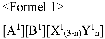 wobei in Formel 1A1 zumindest ein einwertiges organisches Kation, zumindest ein einwertiges anorganisches Kation oder eine beliebige Kombination davon ist,B1 zumindest ein zweiwertiges anorganisches Kation ist,X1 und Y1 jeweils unabhängig zumindest ein einwertiges Anion sind, undn eine reelle Zahl ist, die 0 < n < 3 erfüllt, und
 wobei in Formel 2A2 zumindest ein einwertiges organisches Kation, zumindest ein einwertiges anorganisches Kation oder eine beliebige Kombination davon ist,B2 zumindest ein zweiwertiges anorganisches Kation ist,X2 und Y2 jeweils unabhängig zumindest ein einwertiges Anion sind, undm eine reelle Zahl ist, die 0 < m < 3 erfüllt; unddadurch gekennzeichnet, dassdie Elektronenblockierschicht ferner ein polares Polymer in einer Menge von 5 bis 60 Gewichtsteilen in Bezug auf 100 Gewichtsteile der ersten Perowskitverbindung umfasst, die durch Formel 1 dargestellt ist.
 - Verfahren nach Anspruch 12, wobei die Lochblockierschicht ferner ein polares Polymer umfasst; und/oder
wobei das Bilden der Elektronenblockierschicht Folgendes umfasst: Schleuderbeschichten einer Mischung aus einem Vorläufer der ersten Perowskitverbindung, die durch Formel 1 dargestellt ist, und einem polaren Polymer oder einem Vorläufer davon auf die erste leitende Schicht und thermisches Behandeln einer resultierenden Struktur bei 100 °C bis 300 °C. - Verfahren nach Anspruch 12 oder 13, wobei das Bilden der photoelektrischen Umwandlungsschicht Folgendes umfasst:(a) Hinzufügen eines Nichtlösungsmittels zu einer Mischung, die einen A3-enthaltenden Vorläufer, einen B3-enthaltenden Vorläufer und ein Lösungsmittel beinhaltet, und Rühren bei einer Temperatur von 70 °C bis 120 °C, um eine Lösung einer dritten Perowskitverbindung, die durch Formel 3 dargestellt ist, herzustellen; und(b) Beschichten der Lösung der dritten Perowskitverbindung auf der Elektronenblockierschicht durch Rakelbeschichten oder Stabbeschichten:
 A3 zumindest ein einwertiges organisches Kation, zumindest ein einwertiges anorganisches Kation oder eine beliebige Kombination davon ist,B3 zumindest ein zweiwertiges anorganisches Kation ist,X3 und Y3 jeweils unabhängig zumindest ein einwertiges Anion sind, undk eine reelle Zahl ist, die 0 < k < 3 erfüllt,das Lösungsmittel Dimethylformamid, Dimethylsulfoxid, γ-Butyrolacton oder eine beliebige Kombination davon ist, unddas Nichtlösungsmittel α-Terpineol, Hexylcarbitol, Butylcarbitolacetat, Hexylcellosolve, Butylcellosolveacetat oder eine beliebige Kombination davon ist.
 - Bildgebungsvorrichtung, die eine Lichtbestrahlungseinheit, eine Photodetektoreinheit und eine Steuereinheit umfasst, wobei die Photodetektoreinheit die photoelektrische Umwandlungsvorrichtung nach einem der Ansprüche 1 bis 11 umfasst.
Applications Claiming Priority (2)
| Application Number | Priority Date | Filing Date | Title |
|---|---|---|---|
| KR20170033871 | 2017-03-17 | ||
| KR1020180003467A KR102506443B1 (ko) | 2017-03-17 | 2018-01-10 | 페로브스카이트 화합물을 포함하는 광전 변환 소자 및 이를 포함하는 촬상 장치 |
Publications (2)
| Publication Number | Publication Date |
|---|---|
| EP3379592A1 EP3379592A1 (de) | 2018-09-26 |
| EP3379592B1 true EP3379592B1 (de) | 2023-02-22 |
Family
ID=61626928
Family Applications (1)
| Application Number | Title | Priority Date | Filing Date |
|---|---|---|---|
| EP18161006.4A Active EP3379592B1 (de) | 2017-03-17 | 2018-03-09 | Umwandlungsvorrichtung mit perowskitverbindung, verfahren zur herstellung davon und bildgebungsvorrichtung damit |
Country Status (4)
| Country | Link |
|---|---|
| US (2) | US10903252B2 (de) |
| EP (1) | EP3379592B1 (de) |
| JP (1) | JP7274262B2 (de) |
| CN (1) | CN108630816B (de) |
Families Citing this family (17)
| Publication number | Priority date | Publication date | Assignee | Title |
|---|---|---|---|---|
| CN109627253B (zh) * | 2018-11-21 | 2021-04-27 | 中节能万润股份有限公司 | 一种含有蝶结构的二酸酐及其合成方法以及基于该二酸酐合成的聚酰亚胺 |
| WO2020217783A1 (ja) * | 2019-04-25 | 2020-10-29 | パナソニックIpマネジメント株式会社 | 撮像装置 |
| US11895855B2 (en) | 2019-08-29 | 2024-02-06 | Samsung Electronics Co., Ltd. | Light-emitting device |
| EP3863059B1 (de) | 2020-02-04 | 2024-07-31 | Siemens Healthineers AG | Perowskit-basierte detektoren mit erhöhter adhäsion |
| EP3863054A1 (de) * | 2020-02-04 | 2021-08-11 | Siemens Healthcare GmbH | Multiple spektrale detektoren mittels strukturierter perowskite |
| CN111599827A (zh) * | 2020-04-28 | 2020-08-28 | 深圳市惠能材料科技研发中心(有限合伙) | 一种新型的钙钛矿半导体型x射线探测器及其制备方法 |
| EP3916819A1 (de) * | 2020-05-29 | 2021-12-01 | Nederlandse Organisatie voor toegepast- natuurwetenschappelijk Onderzoek TNO | Perowskitschicht |
| CN112909116B (zh) * | 2021-01-18 | 2023-08-04 | 华中科技大学 | 一种基于介电层响应的场效应管光电探测器 |
| CN112694263A (zh) * | 2021-02-09 | 2021-04-23 | 上海应用技术大学 | 分子铁电体复合CsPbBr3光电薄膜材料、制备方法和应用 |
| CN113823740A (zh) * | 2021-08-05 | 2021-12-21 | 中国科学院深圳先进技术研究院 | n-i结构钙钛矿基X光探测器及其制备方法 |
| TWI781720B (zh) * | 2021-08-10 | 2022-10-21 | 友達光電股份有限公司 | 光偵測裝置 |
| IT202100026675A1 (it) * | 2021-10-18 | 2023-04-18 | Eni Spa | Celle fotovoltaiche semitrasparenti a base di perovskite e procedimento per la loro preparazione. |
| EP4480012A1 (de) * | 2022-02-17 | 2024-12-25 | UVIC Industry Partnerships Inc. | Orthorhombische cspbi3-mikrodrähte für empfindliche flexible hochauflösende röntgendetektoren |
| IT202200012323A1 (it) * | 2022-06-10 | 2023-12-10 | Eni Spa | Celle fotovoltaiche a base di perovskite e procedimento per la loro preparazione |
| US12225273B2 (en) * | 2022-07-26 | 2025-02-11 | Visera Technologies Company Ltd. | Image sensor and control method thereof |
| TWI831509B (zh) | 2022-12-08 | 2024-02-01 | 財團法人工業技術研究院 | 鈣鈦礦厚膜、其製備方法以及包含其之輻射偵測器 |
| JP7564514B1 (ja) * | 2023-03-15 | 2024-10-09 | 三菱瓦斯化学株式会社 | 化合物、有機薄膜、光電変換素子、撮像素子、光センサー及び固体撮像装置 |
Family Cites Families (24)
| Publication number | Priority date | Publication date | Assignee | Title |
|---|---|---|---|---|
| JP3714918B2 (ja) * | 2001-07-31 | 2005-11-09 | 独立行政法人科学技術振興機構 | 放射線検出装置 |
| US6680067B2 (en) * | 2001-11-26 | 2004-01-20 | Oliver Yoa-Pu Hu | Controlled-release pharmaceutical preparation containing nalbuphine and a process for preparing the same |
| JP5093694B2 (ja) | 2008-02-19 | 2012-12-12 | 独立行政法人産業技術総合研究所 | 酸化物ぺロブスカイト薄膜el素子 |
| GB201208793D0 (en) | 2012-05-18 | 2012-07-04 | Isis Innovation | Optoelectronic device |
| EP2846371A1 (de) | 2013-09-10 | 2015-03-11 | Ecole Polytechnique Fédérale de Lausanne (EPFL) | Umgekehrte Solarzelle und Verfahren zur Herstellung davon |
| PL3084854T3 (pl) * | 2013-12-17 | 2020-07-13 | Oxford University Innovation Limited | Urządzenie fotowoltaiczne zawierające perowskit halogenku metalu i środek pasywujący |
| US9583724B2 (en) | 2013-12-19 | 2017-02-28 | Nutech Ventures | Systems and methods for scalable perovskite device fabrication |
| AU2015222678B2 (en) | 2014-02-26 | 2018-11-22 | Commonwealth Scientific And Industrial Research Organisation | Process of forming a photoactive layer of a perovskite photoactive device |
| KR101666563B1 (ko) | 2014-04-28 | 2016-10-27 | 성균관대학교산학협력단 | 페로브스카이트 태양전지 및 그의 제조 방법 |
| EP2942826B1 (de) * | 2014-05-09 | 2023-03-01 | Novaled GmbH | Dotierte perovskite und deren verwendung als aktive und/oder ladungstransportschichten in optoelektronischen vorrichtungen |
| US9349967B2 (en) | 2014-07-16 | 2016-05-24 | Industrial Technology Research Institute | Solar cell and method for manufacturing the same |
| US10297754B2 (en) * | 2014-08-01 | 2019-05-21 | International Business Machines Corporation | Techniques for perovskite layer crystallization |
| TWI556460B (zh) | 2014-09-17 | 2016-11-01 | 國立臺灣大學 | 鈣鈦礦結構基太陽能電池 |
| DE102014225541A1 (de) | 2014-12-11 | 2016-06-16 | Siemens Healthcare Gmbh | Detektionsschicht umfassend Perowskitkristalle |
| US10249441B2 (en) * | 2015-01-21 | 2019-04-02 | Commonwealth Scientific And Industrial Research Organisation | Process of forming a photoactive layer of a perovskite photoactive device |
| JP2016134570A (ja) | 2015-01-21 | 2016-07-25 | パナソニックIpマネジメント株式会社 | 有機光電変換材料、光電変換素子および撮像装置 |
| CN104716263B (zh) | 2015-03-18 | 2017-05-03 | 河南科技大学 | 一种制备混合卤化物钙钛矿CH3NH3PbI3‑xClx梯度膜的方法 |
| JP6754156B2 (ja) | 2015-06-15 | 2020-09-09 | ソニーセミコンダクタソリューションズ株式会社 | 固体撮像素子および固体撮像素子の製造方法、光電変換素子、撮像装置、電子機器、並びに光電変換素子。 |
| JP6687025B2 (ja) | 2015-07-02 | 2020-04-22 | 住友化学株式会社 | 光電変換素子 |
| US9905765B2 (en) | 2015-08-13 | 2018-02-27 | Florida State University Research Foundation, Inc. | Polymer-perovskite films, devices, and methods |
| JP6670138B2 (ja) | 2016-03-14 | 2020-03-18 | 株式会社カネカ | 光電変換装置およびその製造方法 |
| CN105679807B (zh) | 2016-04-15 | 2020-04-28 | 深圳市华星光电技术有限公司 | Oled显示器件及其制作方法 |
| KR102629585B1 (ko) | 2016-10-04 | 2024-01-25 | 삼성전자주식회사 | 광전 변환 소자 및 이를 포함하는 촬상 장치 |
| CN106449990A (zh) | 2016-12-04 | 2017-02-22 | 天津市职业大学 | 一种钙钛矿太阳电池用卤化铯铅的生产方法 |
-
2018
- 2018-03-09 EP EP18161006.4A patent/EP3379592B1/de active Active
- 2018-03-13 JP JP2018045249A patent/JP7274262B2/ja active Active
- 2018-03-14 CN CN201810208331.2A patent/CN108630816B/zh active Active
- 2018-03-15 US US15/922,103 patent/US10903252B2/en active Active
-
2020
- 2020-12-21 US US17/128,416 patent/US11728353B2/en active Active
Also Published As
| Publication number | Publication date |
|---|---|
| EP3379592A1 (de) | 2018-09-26 |
| US11728353B2 (en) | 2023-08-15 |
| US20210118920A1 (en) | 2021-04-22 |
| JP7274262B2 (ja) | 2023-05-16 |
| JP2018157204A (ja) | 2018-10-04 |
| US10903252B2 (en) | 2021-01-26 |
| CN108630816B (zh) | 2022-12-09 |
| US20180269235A1 (en) | 2018-09-20 |
| CN108630816A (zh) | 2018-10-09 |
Similar Documents
| Publication | Publication Date | Title |
|---|---|---|
| EP3379592B1 (de) | Umwandlungsvorrichtung mit perowskitverbindung, verfahren zur herstellung davon und bildgebungsvorrichtung damit | |
| KR102506443B1 (ko) | 페로브스카이트 화합물을 포함하는 광전 변환 소자 및 이를 포함하는 촬상 장치 | |
| EP3988969B1 (de) | Selbstangetriebener perowskit-röntgenstrahlendetektor | |
| Kim et al. | Printable organometallic perovskite enables large-area, low-dose X-ray imaging | |
| Lintangpradipto et al. | Single-crystal methylammonium-free perovskite solar cells with efficiencies exceeding 24% and high thermal stability | |
| Ballantyne et al. | Studies of highly regioregular poly (3-hexylselenophene) for photovoltaic applications | |
| US10263043B2 (en) | Coating made of a semiconductor material | |
| Li et al. | Direct conversion X-ray detectors with 70 pA cm− 2 dark currents coated from an alcohol-based perovskite ink | |
| Chen et al. | Efficient aqueous-processed hybrid solar cells from a polymer with a wide bandgap | |
| Tao et al. | Efficient photodiode-type photodetectors with perovskite thin films derived from an MAPbI 3 single-crystal precursor | |
| Miyazawa et al. | Evaluation of damage coefficient for minority-carrier diffusion length of triple-cation perovskite solar cells under 1 MeV electron irradiation for space applications | |
| Manmohan et al. | Up and down conversion of photons with modified perturb and observe MPPT technique for efficient solar energy generation | |
| US10210998B2 (en) | Photoelectric conversion device and imaging device including the same | |
| CN116367686B (zh) | 钙钛矿光伏电池、钙钛矿光伏电池组件和用电装置 | |
| CN116156905B (zh) | 功能层、太阳能电池和用电装置 | |
| Yang et al. | Characterizations and understanding of additives induced passivation effects in narrow-bandgap Sn–Pb alloyed perovskite solar cells | |
| Yerramilli et al. | Passivation of triple cation perovskites using guanidinium iodide in inverted solar cells for improved open-circuit voltage and stability | |
| Wang et al. | New Insight into Sulfurized and Selenized Kesterite–Titania Nanostructures for CdS-free and HTM-free Photovoltaic and Voltage-Modulated Photodetecting Applications | |
| Dias et al. | CH3NH3PbBr3 quantum dots for visible wavelength photodetector applications | |
| Xu et al. | Perovskites–revisiting the venerable ABX 3 family with organic flexibility and new applications | |
| Nienhaus et al. | Solid-state infrared-to-visible upconversion for sub-bandgap sensitization of photovoltaics | |
| CN116156906B (zh) | 光转换层、太阳能电池和用电装置 | |
| Althumairi et al. | Structure and Photocapacitance characteristics of nanosized coumarin-based dye for organic light-dependent resistor applications | |
| CN119136632A (zh) | 钙钛矿前驱体溶液、钙钛矿太阳能电池及其制备方法 | |
| Ahme | Spectroscopic investigations of transfer and transport of charge carriers in the donor/acceptor network of organic solar cells |
Legal Events
| Date | Code | Title | Description |
|---|---|---|---|
| PUAI | Public reference made under article 153(3) epc to a published international application that has entered the european phase |
Free format text: ORIGINAL CODE: 0009012 |
|
| STAA | Information on the status of an ep patent application or granted ep patent |
Free format text: STATUS: THE APPLICATION HAS BEEN PUBLISHED |
|
| AK | Designated contracting states |
Kind code of ref document: A1 Designated state(s): AL AT BE BG CH CY CZ DE DK EE ES FI FR GB GR HR HU IE IS IT LI LT LU LV MC MK MT NL NO PL PT RO RS SE SI SK SM TR |
|
| AX | Request for extension of the european patent |
Extension state: BA ME |
|
| STAA | Information on the status of an ep patent application or granted ep patent |
Free format text: STATUS: REQUEST FOR EXAMINATION WAS MADE |
|
| 17P | Request for examination filed |
Effective date: 20190326 |
|
| RBV | Designated contracting states (corrected) |
Designated state(s): AL AT BE BG CH CY CZ DE DK EE ES FI FR GB GR HR HU IE IS IT LI LT LU LV MC MK MT NL NO PL PT RO RS SE SI SK SM TR |
|
| STAA | Information on the status of an ep patent application or granted ep patent |
Free format text: STATUS: EXAMINATION IS IN PROGRESS |
|
| 17Q | First examination report despatched |
Effective date: 20210616 |
|
| GRAP | Despatch of communication of intention to grant a patent |
Free format text: ORIGINAL CODE: EPIDOSNIGR1 |
|
| STAA | Information on the status of an ep patent application or granted ep patent |
Free format text: STATUS: GRANT OF PATENT IS INTENDED |
|
| INTG | Intention to grant announced |
Effective date: 20220907 |
|
| RIN1 | Information on inventor provided before grant (corrected) |
Inventor name: KIM, YONGCHUL |
|
| GRAS | Grant fee paid |
Free format text: ORIGINAL CODE: EPIDOSNIGR3 |
|
| GRAA | (expected) grant |
Free format text: ORIGINAL CODE: 0009210 |
|
| STAA | Information on the status of an ep patent application or granted ep patent |
Free format text: STATUS: THE PATENT HAS BEEN GRANTED |
|
| AK | Designated contracting states |
Kind code of ref document: B1 Designated state(s): AL AT BE BG CH CY CZ DE DK EE ES FI FR GB GR HR HU IE IS IT LI LT LU LV MC MK MT NL NO PL PT RO RS SE SI SK SM TR |
|
| REG | Reference to a national code |
Ref country code: GB Ref legal event code: FG4D |
|
| REG | Reference to a national code |
Ref country code: CH Ref legal event code: EP |
|
| REG | Reference to a national code |
Ref country code: DE Ref legal event code: R096 Ref document number: 602018046331 Country of ref document: DE |
|
| REG | Reference to a national code |
Ref country code: AT Ref legal event code: REF Ref document number: 1550083 Country of ref document: AT Kind code of ref document: T Effective date: 20230315 Ref country code: IE Ref legal event code: FG4D |
|
| REG | Reference to a national code |
Ref country code: LT Ref legal event code: MG9D |
|
| P01 | Opt-out of the competence of the unified patent court (upc) registered |
Effective date: 20230520 |
|
| REG | Reference to a national code |
Ref country code: NL Ref legal event code: MP Effective date: 20230222 |
|
| REG | Reference to a national code |
Ref country code: AT Ref legal event code: MK05 Ref document number: 1550083 Country of ref document: AT Kind code of ref document: T Effective date: 20230222 |
|
| PG25 | Lapsed in a contracting state [announced via postgrant information from national office to epo] |
Ref country code: RS Free format text: LAPSE BECAUSE OF FAILURE TO SUBMIT A TRANSLATION OF THE DESCRIPTION OR TO PAY THE FEE WITHIN THE PRESCRIBED TIME-LIMIT Effective date: 20230222 Ref country code: PT Free format text: LAPSE BECAUSE OF FAILURE TO SUBMIT A TRANSLATION OF THE DESCRIPTION OR TO PAY THE FEE WITHIN THE PRESCRIBED TIME-LIMIT Effective date: 20230622 Ref country code: NO Free format text: LAPSE BECAUSE OF FAILURE TO SUBMIT A TRANSLATION OF THE DESCRIPTION OR TO PAY THE FEE WITHIN THE PRESCRIBED TIME-LIMIT Effective date: 20230522 Ref country code: NL Free format text: LAPSE BECAUSE OF FAILURE TO SUBMIT A TRANSLATION OF THE DESCRIPTION OR TO PAY THE FEE WITHIN THE PRESCRIBED TIME-LIMIT Effective date: 20230222 Ref country code: LV Free format text: LAPSE BECAUSE OF FAILURE TO SUBMIT A TRANSLATION OF THE DESCRIPTION OR TO PAY THE FEE WITHIN THE PRESCRIBED TIME-LIMIT Effective date: 20230222 Ref country code: LT Free format text: LAPSE BECAUSE OF FAILURE TO SUBMIT A TRANSLATION OF THE DESCRIPTION OR TO PAY THE FEE WITHIN THE PRESCRIBED TIME-LIMIT Effective date: 20230222 Ref country code: HR Free format text: LAPSE BECAUSE OF FAILURE TO SUBMIT A TRANSLATION OF THE DESCRIPTION OR TO PAY THE FEE WITHIN THE PRESCRIBED TIME-LIMIT Effective date: 20230222 Ref country code: ES Free format text: LAPSE BECAUSE OF FAILURE TO SUBMIT A TRANSLATION OF THE DESCRIPTION OR TO PAY THE FEE WITHIN THE PRESCRIBED TIME-LIMIT Effective date: 20230222 Ref country code: AT Free format text: LAPSE BECAUSE OF FAILURE TO SUBMIT A TRANSLATION OF THE DESCRIPTION OR TO PAY THE FEE WITHIN THE PRESCRIBED TIME-LIMIT Effective date: 20230222 |
|
| PG25 | Lapsed in a contracting state [announced via postgrant information from national office to epo] |
Ref country code: SE Free format text: LAPSE BECAUSE OF FAILURE TO SUBMIT A TRANSLATION OF THE DESCRIPTION OR TO PAY THE FEE WITHIN THE PRESCRIBED TIME-LIMIT Effective date: 20230222 Ref country code: PL Free format text: LAPSE BECAUSE OF FAILURE TO SUBMIT A TRANSLATION OF THE DESCRIPTION OR TO PAY THE FEE WITHIN THE PRESCRIBED TIME-LIMIT Effective date: 20230222 Ref country code: IS Free format text: LAPSE BECAUSE OF FAILURE TO SUBMIT A TRANSLATION OF THE DESCRIPTION OR TO PAY THE FEE WITHIN THE PRESCRIBED TIME-LIMIT Effective date: 20230622 Ref country code: GR Free format text: LAPSE BECAUSE OF FAILURE TO SUBMIT A TRANSLATION OF THE DESCRIPTION OR TO PAY THE FEE WITHIN THE PRESCRIBED TIME-LIMIT Effective date: 20230523 Ref country code: FI Free format text: LAPSE BECAUSE OF FAILURE TO SUBMIT A TRANSLATION OF THE DESCRIPTION OR TO PAY THE FEE WITHIN THE PRESCRIBED TIME-LIMIT Effective date: 20230222 |
|
| PG25 | Lapsed in a contracting state [announced via postgrant information from national office to epo] |
Ref country code: SM Free format text: LAPSE BECAUSE OF FAILURE TO SUBMIT A TRANSLATION OF THE DESCRIPTION OR TO PAY THE FEE WITHIN THE PRESCRIBED TIME-LIMIT Effective date: 20230222 Ref country code: RO Free format text: LAPSE BECAUSE OF FAILURE TO SUBMIT A TRANSLATION OF THE DESCRIPTION OR TO PAY THE FEE WITHIN THE PRESCRIBED TIME-LIMIT Effective date: 20230222 Ref country code: EE Free format text: LAPSE BECAUSE OF FAILURE TO SUBMIT A TRANSLATION OF THE DESCRIPTION OR TO PAY THE FEE WITHIN THE PRESCRIBED TIME-LIMIT Effective date: 20230222 Ref country code: DK Free format text: LAPSE BECAUSE OF FAILURE TO SUBMIT A TRANSLATION OF THE DESCRIPTION OR TO PAY THE FEE WITHIN THE PRESCRIBED TIME-LIMIT Effective date: 20230222 Ref country code: CZ Free format text: LAPSE BECAUSE OF FAILURE TO SUBMIT A TRANSLATION OF THE DESCRIPTION OR TO PAY THE FEE WITHIN THE PRESCRIBED TIME-LIMIT Effective date: 20230222 |
|
| REG | Reference to a national code |
Ref country code: CH Ref legal event code: PL |
|
| REG | Reference to a national code |
Ref country code: DE Ref legal event code: R097 Ref document number: 602018046331 Country of ref document: DE |
|
| PG25 | Lapsed in a contracting state [announced via postgrant information from national office to epo] |
Ref country code: SK Free format text: LAPSE BECAUSE OF FAILURE TO SUBMIT A TRANSLATION OF THE DESCRIPTION OR TO PAY THE FEE WITHIN THE PRESCRIBED TIME-LIMIT Effective date: 20230222 |
|
| REG | Reference to a national code |
Ref country code: BE Ref legal event code: MM Effective date: 20230331 |
|
| PG25 | Lapsed in a contracting state [announced via postgrant information from national office to epo] |
Ref country code: LU Free format text: LAPSE BECAUSE OF NON-PAYMENT OF DUE FEES Effective date: 20230309 |
|
| PLBE | No opposition filed within time limit |
Free format text: ORIGINAL CODE: 0009261 |
|
| STAA | Information on the status of an ep patent application or granted ep patent |
Free format text: STATUS: NO OPPOSITION FILED WITHIN TIME LIMIT |
|
| PG25 | Lapsed in a contracting state [announced via postgrant information from national office to epo] |
Ref country code: MC Free format text: LAPSE BECAUSE OF FAILURE TO SUBMIT A TRANSLATION OF THE DESCRIPTION OR TO PAY THE FEE WITHIN THE PRESCRIBED TIME-LIMIT Effective date: 20230222 |
|
| REG | Reference to a national code |
Ref country code: IE Ref legal event code: MM4A |
|
| 26N | No opposition filed |
Effective date: 20231123 |
|
| PG25 | Lapsed in a contracting state [announced via postgrant information from national office to epo] |
Ref country code: SI Free format text: LAPSE BECAUSE OF FAILURE TO SUBMIT A TRANSLATION OF THE DESCRIPTION OR TO PAY THE FEE WITHIN THE PRESCRIBED TIME-LIMIT Effective date: 20230222 Ref country code: MC Free format text: LAPSE BECAUSE OF FAILURE TO SUBMIT A TRANSLATION OF THE DESCRIPTION OR TO PAY THE FEE WITHIN THE PRESCRIBED TIME-LIMIT Effective date: 20230222 Ref country code: LI Free format text: LAPSE BECAUSE OF NON-PAYMENT OF DUE FEES Effective date: 20230331 Ref country code: IE Free format text: LAPSE BECAUSE OF NON-PAYMENT OF DUE FEES Effective date: 20230309 Ref country code: CH Free format text: LAPSE BECAUSE OF NON-PAYMENT OF DUE FEES Effective date: 20230331 |
|
| PG25 | Lapsed in a contracting state [announced via postgrant information from national office to epo] |
Ref country code: BE Free format text: LAPSE BECAUSE OF NON-PAYMENT OF DUE FEES Effective date: 20230331 |
|
| PG25 | Lapsed in a contracting state [announced via postgrant information from national office to epo] |
Ref country code: IT Free format text: LAPSE BECAUSE OF FAILURE TO SUBMIT A TRANSLATION OF THE DESCRIPTION OR TO PAY THE FEE WITHIN THE PRESCRIBED TIME-LIMIT Effective date: 20230222 |
|
| PG25 | Lapsed in a contracting state [announced via postgrant information from national office to epo] |
Ref country code: BG Free format text: LAPSE BECAUSE OF FAILURE TO SUBMIT A TRANSLATION OF THE DESCRIPTION OR TO PAY THE FEE WITHIN THE PRESCRIBED TIME-LIMIT Effective date: 20230222 |
|
| PG25 | Lapsed in a contracting state [announced via postgrant information from national office to epo] |
Ref country code: BG Free format text: LAPSE BECAUSE OF FAILURE TO SUBMIT A TRANSLATION OF THE DESCRIPTION OR TO PAY THE FEE WITHIN THE PRESCRIBED TIME-LIMIT Effective date: 20230222 |
|
| PG25 | Lapsed in a contracting state [announced via postgrant information from national office to epo] |
Ref country code: CY Free format text: LAPSE BECAUSE OF FAILURE TO SUBMIT A TRANSLATION OF THE DESCRIPTION OR TO PAY THE FEE WITHIN THE PRESCRIBED TIME-LIMIT; INVALID AB INITIO Effective date: 20180309 |
|
| PG25 | Lapsed in a contracting state [announced via postgrant information from national office to epo] |
Ref country code: HU Free format text: LAPSE BECAUSE OF FAILURE TO SUBMIT A TRANSLATION OF THE DESCRIPTION OR TO PAY THE FEE WITHIN THE PRESCRIBED TIME-LIMIT; INVALID AB INITIO Effective date: 20180309 |
|
| PG25 | Lapsed in a contracting state [announced via postgrant information from national office to epo] |
Ref country code: TR Free format text: LAPSE BECAUSE OF FAILURE TO SUBMIT A TRANSLATION OF THE DESCRIPTION OR TO PAY THE FEE WITHIN THE PRESCRIBED TIME-LIMIT Effective date: 20230222 |
|
| PGFP | Annual fee paid to national office [announced via postgrant information from national office to epo] |
Ref country code: GB Payment date: 20260216 Year of fee payment: 9 |
|
| PGFP | Annual fee paid to national office [announced via postgrant information from national office to epo] |
Ref country code: DE Payment date: 20260211 Year of fee payment: 9 |
|
| PGFP | Annual fee paid to national office [announced via postgrant information from national office to epo] |
Ref country code: FR Payment date: 20260209 Year of fee payment: 9 |