EP3379663B1 - Laser verrouillé à mode hybride ayant un nombre accordable de lignes de peigne - Google Patents
Laser verrouillé à mode hybride ayant un nombre accordable de lignes de peigne Download PDFInfo
- Publication number
- EP3379663B1 EP3379663B1 EP18160158.4A EP18160158A EP3379663B1 EP 3379663 B1 EP3379663 B1 EP 3379663B1 EP 18160158 A EP18160158 A EP 18160158A EP 3379663 B1 EP3379663 B1 EP 3379663B1
- Authority
- EP
- European Patent Office
- Prior art keywords
- silicon
- mode
- locked
- wavelengths
- optical
- Prior art date
- Legal status (The legal status is an assumption and is not a legal conclusion. Google has not performed a legal analysis and makes no representation as to the accuracy of the status listed.)
- Active
Links
Images



Classifications
-
- H—ELECTRICITY
- H01—ELECTRIC ELEMENTS
- H01S—DEVICES USING THE PROCESS OF LIGHT AMPLIFICATION BY STIMULATED EMISSION OF RADIATION [LASER] TO AMPLIFY OR GENERATE LIGHT; DEVICES USING STIMULATED EMISSION OF ELECTROMAGNETIC RADIATION IN WAVE RANGES OTHER THAN OPTICAL
- H01S5/00—Semiconductor lasers
- H01S5/10—Construction or shape of the optical resonator, e.g. extended or external cavity, coupled cavities, bent-guide, varying width, thickness or composition of the active region
- H01S5/1092—Multi-wavelength lasing
-
- H—ELECTRICITY
- H01—ELECTRIC ELEMENTS
- H01S—DEVICES USING THE PROCESS OF LIGHT AMPLIFICATION BY STIMULATED EMISSION OF RADIATION [LASER] TO AMPLIFY OR GENERATE LIGHT; DEVICES USING STIMULATED EMISSION OF ELECTROMAGNETIC RADIATION IN WAVE RANGES OTHER THAN OPTICAL
- H01S5/00—Semiconductor lasers
- H01S5/06—Arrangements for controlling the laser output parameters, e.g. by operating on the active medium
- H01S5/065—Mode locking; Mode suppression; Mode selection ; Self pulsating
- H01S5/0657—Mode locking, i.e. generation of pulses at a frequency corresponding to a roundtrip in the cavity
-
- H—ELECTRICITY
- H01—ELECTRIC ELEMENTS
- H01S—DEVICES USING THE PROCESS OF LIGHT AMPLIFICATION BY STIMULATED EMISSION OF RADIATION [LASER] TO AMPLIFY OR GENERATE LIGHT; DEVICES USING STIMULATED EMISSION OF ELECTROMAGNETIC RADIATION IN WAVE RANGES OTHER THAN OPTICAL
- H01S5/00—Semiconductor lasers
- H01S5/005—Optical components external to the laser cavity, specially adapted therefor, e.g. for homogenisation or merging of the beams or for manipulating laser pulses, e.g. pulse shaping
- H01S5/0078—Optical components external to the laser cavity, specially adapted therefor, e.g. for homogenisation or merging of the beams or for manipulating laser pulses, e.g. pulse shaping for frequency filtering
-
- H—ELECTRICITY
- H01—ELECTRIC ELEMENTS
- H01S—DEVICES USING THE PROCESS OF LIGHT AMPLIFICATION BY STIMULATED EMISSION OF RADIATION [LASER] TO AMPLIFY OR GENERATE LIGHT; DEVICES USING STIMULATED EMISSION OF ELECTROMAGNETIC RADIATION IN WAVE RANGES OTHER THAN OPTICAL
- H01S5/00—Semiconductor lasers
- H01S5/10—Construction or shape of the optical resonator, e.g. extended or external cavity, coupled cavities, bent-guide, varying width, thickness or composition of the active region
- H01S5/14—External cavity lasers
- H01S5/141—External cavity lasers using a wavelength selective device, e.g. a grating or etalon
-
- H—ELECTRICITY
- H01—ELECTRIC ELEMENTS
- H01S—DEVICES USING THE PROCESS OF LIGHT AMPLIFICATION BY STIMULATED EMISSION OF RADIATION [LASER] TO AMPLIFY OR GENERATE LIGHT; DEVICES USING STIMULATED EMISSION OF ELECTROMAGNETIC RADIATION IN WAVE RANGES OTHER THAN OPTICAL
- H01S5/00—Semiconductor lasers
- H01S5/10—Construction or shape of the optical resonator, e.g. extended or external cavity, coupled cavities, bent-guide, varying width, thickness or composition of the active region
- H01S5/14—External cavity lasers
- H01S5/141—External cavity lasers using a wavelength selective device, e.g. a grating or etalon
- H01S5/142—External cavity lasers using a wavelength selective device, e.g. a grating or etalon which comprises an additional resonator
-
- H—ELECTRICITY
- H01—ELECTRIC ELEMENTS
- H01S—DEVICES USING THE PROCESS OF LIGHT AMPLIFICATION BY STIMULATED EMISSION OF RADIATION [LASER] TO AMPLIFY OR GENERATE LIGHT; DEVICES USING STIMULATED EMISSION OF ELECTROMAGNETIC RADIATION IN WAVE RANGES OTHER THAN OPTICAL
- H01S3/00—Lasers, i.e. devices using stimulated emission of electromagnetic radiation in the infrared, visible or ultraviolet wave range
- H01S3/10—Controlling the intensity, frequency, phase, polarisation or direction of the emitted radiation, e.g. switching, gating, modulating or demodulating
- H01S3/106—Controlling the intensity, frequency, phase, polarisation or direction of the emitted radiation, e.g. switching, gating, modulating or demodulating by controlling devices placed within the cavity
- H01S3/1061—Controlling the intensity, frequency, phase, polarisation or direction of the emitted radiation, e.g. switching, gating, modulating or demodulating by controlling devices placed within the cavity using a variable absorption device
-
- H—ELECTRICITY
- H01—ELECTRIC ELEMENTS
- H01S—DEVICES USING THE PROCESS OF LIGHT AMPLIFICATION BY STIMULATED EMISSION OF RADIATION [LASER] TO AMPLIFY OR GENERATE LIGHT; DEVICES USING STIMULATED EMISSION OF ELECTROMAGNETIC RADIATION IN WAVE RANGES OTHER THAN OPTICAL
- H01S3/00—Lasers, i.e. devices using stimulated emission of electromagnetic radiation in the infrared, visible or ultraviolet wave range
- H01S3/10—Controlling the intensity, frequency, phase, polarisation or direction of the emitted radiation, e.g. switching, gating, modulating or demodulating
- H01S3/106—Controlling the intensity, frequency, phase, polarisation or direction of the emitted radiation, e.g. switching, gating, modulating or demodulating by controlling devices placed within the cavity
- H01S3/1062—Controlling the intensity, frequency, phase, polarisation or direction of the emitted radiation, e.g. switching, gating, modulating or demodulating by controlling devices placed within the cavity using a controlled passive interferometer, e.g. a Fabry-Perot etalon
-
- H—ELECTRICITY
- H01—ELECTRIC ELEMENTS
- H01S—DEVICES USING THE PROCESS OF LIGHT AMPLIFICATION BY STIMULATED EMISSION OF RADIATION [LASER] TO AMPLIFY OR GENERATE LIGHT; DEVICES USING STIMULATED EMISSION OF ELECTROMAGNETIC RADIATION IN WAVE RANGES OTHER THAN OPTICAL
- H01S5/00—Semiconductor lasers
- H01S5/02—Structural details or components not essential to laser action
- H01S5/0206—Substrates, e.g. growth, shape, material, removal or bonding
- H01S5/021—Silicon based substrates
-
- H—ELECTRICITY
- H01—ELECTRIC ELEMENTS
- H01S—DEVICES USING THE PROCESS OF LIGHT AMPLIFICATION BY STIMULATED EMISSION OF RADIATION [LASER] TO AMPLIFY OR GENERATE LIGHT; DEVICES USING STIMULATED EMISSION OF ELECTROMAGNETIC RADIATION IN WAVE RANGES OTHER THAN OPTICAL
- H01S5/00—Semiconductor lasers
- H01S5/10—Construction or shape of the optical resonator, e.g. extended or external cavity, coupled cavities, bent-guide, varying width, thickness or composition of the active region
- H01S5/1003—Waveguide having a modified shape along the axis, e.g. branched, curved, tapered, voids
- H01S5/101—Curved waveguide
-
- H—ELECTRICITY
- H01—ELECTRIC ELEMENTS
- H01S—DEVICES USING THE PROCESS OF LIGHT AMPLIFICATION BY STIMULATED EMISSION OF RADIATION [LASER] TO AMPLIFY OR GENERATE LIGHT; DEVICES USING STIMULATED EMISSION OF ELECTROMAGNETIC RADIATION IN WAVE RANGES OTHER THAN OPTICAL
- H01S5/00—Semiconductor lasers
- H01S5/10—Construction or shape of the optical resonator, e.g. extended or external cavity, coupled cavities, bent-guide, varying width, thickness or composition of the active region
- H01S5/1082—Construction or shape of the optical resonator, e.g. extended or external cavity, coupled cavities, bent-guide, varying width, thickness or composition of the active region with a special facet structure, e.g. structured, non planar, oblique
- H01S5/1085—Oblique facets
-
- H—ELECTRICITY
- H01—ELECTRIC ELEMENTS
- H01S—DEVICES USING THE PROCESS OF LIGHT AMPLIFICATION BY STIMULATED EMISSION OF RADIATION [LASER] TO AMPLIFY OR GENERATE LIGHT; DEVICES USING STIMULATED EMISSION OF ELECTROMAGNETIC RADIATION IN WAVE RANGES OTHER THAN OPTICAL
- H01S5/00—Semiconductor lasers
- H01S5/50—Amplifier structures not provided for in groups H01S5/02 - H01S5/30
Definitions
- the present invention relates to optical components and in particular to a mode-locked laser.
- Comb sources and multi-frequency lasers are key candidates for enabling the move to lower costs for optical communication systems.
- a comb generator allows for a given laser device to emit at a number of spaced-apart, separate wavelengths ("comb lines").
- comb lines spaced-apart, separate wavelengths
- the introduction of a comb source allows for a single tunable laser source to be shared among several modulators, each modulator utilizing a separate one of the comb lines.
- MLLs mode-locked lasers
- a mode-locked laser and, more particularly, to a hybrid mode-locked laser based upon a combination of a III-V-based gain element and a silicon-based photonic integrated circuit (PIC).
- PIC silicon-based photonic integrated circuit
- One cavity mirror is formed within the III-V element, with the opposing mirror formed within the PIC element (thus creating a "hybrid laser cavity” across the combination of elements).
- An optical wavelength filter component is disposed within the PIC element and positioned along the signal path of the hybrid laser cavity. By controlling the characteristics of the wavelength filter (i.e., wavelengths passed or rejected), the number of mode-locked wavelengths (also referred to at times hereinafter as "comb lines”) generated by the hybrid laser structure is also controlled.
- the optical waveguide filter is formed as a passive device, providing a fixed output of comb lines as a function of the filter passband.
- the optical waveguide filter may be formed as an active device having a tunable passband (tunable in both bandwidth and center wavelength), allowing for the number of generated comb lines to be tuned.
- the tuning may be dynamic and controllable by the user to modify the number of generated comb lines as a function of time.
- the optical filter may incorporate ring resonators, gratings, or any other suitable type of silicon-based optical wavelength filtering component.
- One exemplary embodiment of the present invention takes the form of an apparatus comprising a gain element formed of III-V material and including a first mirror, and a silicon photonic integrated circuit (PIC) coupled to the gain element.
- the silicon PIC includes an optical waveguide coupled at a first end to the gain element, a second mirror coupled to a second end of the optical waveguide (opposing the first end of the optical waveguide).
- the first mirror is formed to exhibit a first reflectivity
- the second mirror is formed to exhibit a second reflectivity which is different from the first reflectivity.
- the first mirror and the second mirror thus define a hybrid laser cavity configured to generate a number of mode-locked output wavelengths.
- the silicon PIC further includes a silicon-based optical filter disposed along the hybrid laser cavity and configured to control the number of mode-locked wavelengths generated as an output of the apparatus.
- Another exemplary embodiment of the present invention defines a method comprising the following: providing III-V gain material having a termination including a mirror facet, providing a silicon-based photonic integrated circuit (PIC) including an optical waveguide (terminating at a mirror element) and an optical filter disposed along the optical waveguide (the optical filter having a tunable passband), coupling the gain material to the photonic circuit so as to create a hybrid laser cavity between the mirror facet of the gain material and the mirror element of the silicon-based PIC, defining a specific number of mode-locked wavelengths, and tuning the optical wavelength filter to pass the defined, specific number of mode-locked wavelengths.
- PIC silicon-based photonic integrated circuit
- optical gain material such as bulk, quantum well, or quantum dot III-V material can be formed into a Fabry-Perot (FP) laser on a III-V chip.
- FP Fabry-Perot
- Multiple modes are generated in such a cavity, and can be actively mode-locked or passively mode-locked by using a saturable absorber or applying four-wave mixing (FWM) to the generated signals.
- FWM four-wave mixing
- FIG. 2 illustrates a typical output from a mode-locked laser (MLL) with an FP cavity length of 170 ⁇ m
- FIG. 2(a) is an autocorrelation trace (time response) showing the generated period to be on the order of 4.07ps
- FIG. 2(b) is the optical spectrum.
- the individual mode-locked wavelengths shown in the spectrum of FIG. 2(b) are defined as the "comb lines", where in this case a relatively large number of individual comb lines are generated.
- the plots shown in FIG. 3 are associated with a typical comb generator having an FP cavity length of 120 ⁇ m.
- the autocorrelation plot of FIG. 3(a) shows a periodicity on the order of 2.86 ps
- the spectrum shown in FIG. 3(b) yields a smaller number of comb lines than the longer cavity associated with plot of FIG. 2(b) .
- a given MLL configuration may not generate enough lines for a specific application (for example, a dense WDM-based optical communication system), thus requiring additional MLLs to be used.
- incorporating a silicon-based filter within the cavity of the MLL gives the system designer the ability to control the number of comb lines generated by the device.
- FIG. 4 is a diagram of a hybrid III-V/silicon mode-locked laser (MLL) 10 that is capable of generating a selected number of comb lines (i.e., mode-locked lasing wavelengths) in accordance with the teachings of the present disclosure.
- MLL 10 is shown as comprising a III-V based semiconductor optical amplifier (SOA) 12, which is optically coupled to a silicon photonic integrated circuit (PIC) 14.
- SOA 12 may comprise any appropriate III-V based type of gain structure typically used including, but not limited to, bulk materials, quantum well structures, quantum dot structures, and the like.
- silicon PIC 14 is formed to include an interface waveguide 16 that is coupled at a first end termination 16-1 to SOA 12.
- a first mirror 18 is disposed at an opposing, far-end termination 16-2 of waveguide 16, where as will be discussed in detail below, first mirror 18 forms one termination of the hybrid laser cavity formed by the combination of SOA 12 and PIC 14.
- first mirror 18 is formed to be fully reflective (e.g., 100% reflectivity).
- an optical filter 20 is shown as disposed between end termination 16-1 of waveguide 16 and first mirror 18.
- optical filter 20 is used to control the specific number of mode-locked wavelengths provided as an output from MLL 10.
- SOA 12 includes an optical waveguide 22 that couples to first end termination 16-1 of silicon PIC waveguide 16.
- a second mirror 24 is formed at an opposing termination of optical waveguide 22, where the combination of second mirror 24, waveguides 22 and 16, and first mirror 18 defines the cavity C of the hybrid III-V/silicon laser structure.
- first mirror 18 is formed as a fully reflective mirror
- second mirror 24 is formed as a partially reflective mirror so that the output radiation from MLL 10 exits via this partially reflective surface, as shown in FIG. 4 .
- optical filter 20 is formed within PIC 14 and is disposed along waveguide 16 between partially reflective mirror 24 and fully reflective mirror 18 (i.e., forming an "intra-cavity filter").
- the parameters of optical filter structure 20 are selected to define the specific number of comb lines (i.e., mode-locked wavelengths) that are ultimately provided as the output of hybrid MLL 10 (in this case, as emitted from mirror 24).
- first mirror 18 may be formed as a partially reflective mirror and second mirror 24 may be formed as a fully reflective mirror. With this alternative positioning of the mirrors, the output "controlled" comb lines from hybrid MLL 10 would exit from first mirror 18.
- FIG. 5 illustrates the principles of operation associated with one or more embodiments of the present invention.
- FIG. 5(a) illustrates the conventional mode-locked response associated with the hybrid laser structure of SOA 12 and PIC 14 when no filtering takes place along waveguide 16.
- the specific mode-locked wavelengths are shown as arrows, with the envelope illustrating the relative gain available at each wavelength as a function of the particular III-V material used in the formation of SOA 12.
- Optical filter 20 may be formed as a passive device, where the number of mode-locked wavelengths (comb lines) remains fixed, or as an active device where the filter characteristics may be tuned to adjust the number of comb lines that are generated.
- Optical filter 20 may be "tunable" at the time of deployment, or may be a dynamic configuration with the continuing ability to change the number of generated comb lines as a function of time.
- specific filter configurations such as ring resonators, coupled ring structures, gratings (including arrayed waveguide gratings), are some of the specific elements that may be used in the formation of optical filter 20.
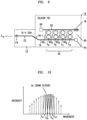
- FIG. 6 illustrates an exemplary embodiment of the present invention, where in this case optical filter 20 comprises a set of eight ring resonators 30 1 , 30 2 , ..., 30 8 , with four rings disposed on either side of waveguide 16.
- each ring 30 i is configured to resonate at a different wavelength ⁇ i , thus coupling light at its resonant wavelength out of optical waveguide 16 and into an associated tap waveguide.
- ring resonators 30 1 , 30 2 , 30 3 and 30 4 are disposed to evanescently couple their respective resonant wavelengths into a first tap waveguide 32.
- Ring resonators 30 5 , 30 6 , 30 7 , and 30 8 are disposed to evanescently couple light at their resonant wavelengths into a second tap waveguide 34.
- Optical absorbers 36 1 and 36 2 are coupled to opposing end terminations of first tap waveguide 32 and function to isolate the filtered wavelengths and prevent any light at these wavelengths from being re-introduced into waveguide 16.
- a pair of optical absorbers 38 1 and 38 2 is similarly disposed at opposing end terminations of second tap waveguide 34 to perform the same isolation function.
- FIG. 7 is a graph depicting the filtering properties of the group of ring resonators 30, showing the how each of the specific wavelengths outside of the selected set ( ⁇ a , ⁇ b , ⁇ c , and ⁇ d ) is removed.
- optical filter 20 is designed to eliminate all of the unwanted comb lines so that MLL 10 only generates the specified number of mode-locked wavelengths.
- FIG. 8 is a plot illustrating the result of this variation, with turning "off" ring resonator 30s.
- MLL 10 provides a set of five comb lines as the output from SOA 12.
- the ability to selectively turn "on” and “off” individual rings allows for the number of generated comb lines to be modified, as needed.
- each ring resonator is tuned to a different wavelength so as to avoid any potential Vernier effect and/or parasitic oscillation within the hybrid cavity.
- optical filter 20 is shown as comprising a set of eight ring resonators 60 disposed in a "coupled" configuration between input waveguide 16 and a return waveguide 62, in this case organized as four separate pairs of coupled rings, denoted as 60 1 , 60 2 , 60 3 , and 60 4 in FIG. 9 .
- a given CROW structure may use any desired number of cascaded rings in a signal path between a pair of waveguides.
- the specific illustration in FIG. 9 where each path includes only a pair of rings is exemplary only.
- each CROW filter element 60 1 , 60 2 , 60 3 , and 60 4 removes all wavelengths except for its defined mode-locked wavelength.
- CROW filter element 60 1 may be configured to have a resonant wavelength ⁇ a
- filter element 60 2 may be configured to have a resonant wavelength ⁇ b
- filter element 60 3 may be configured to have a resonant wavelength ⁇ c
- filter element 60 4 may be configured to have a resonant wavelength ⁇ d .
- the remaining wavelengths created by this mode-locked laser structure are absorbed by either a first absorbing element 64 disposed at the end termination of input waveguide 16, or a second absorbing element 66 disposed at an end termination of the return waveguide 62 (that is, disposed in opposition to first reflecting mirror 18, as shown).
- the hybrid laser arrangement of FIG. 9 will provide a set of four mode-locked wavelengths as the output, as shown by the plot of FIG. 10 .
- the set of mode-locked wavelengths falling within wavelength range A is shown as coupled into a first output waveguide 72 A from AWG 70, with the mode-locked wavelengths falling within wavelength range B coupled into a second output waveguide 72 B .
- the mode-locked wavelengths falling within wavelength range C are coupled into a third output waveguide 72c and the mode-locked wavelengths falling within wavelength range D are coupled into a fourth output waveguide 72 D .
- VOA variable optical attenuators
- 74 A , 74 B , 74 C , and 74 D associated with waveguides 72 in a one-to-one relationship.
- Each waveguide 72 i is shown as terminating in a separate fully reflective mirror 18 i . Therefore, depending on which VOAs are turned "on", specific reflective mirror(s) 18 are used to define the termination of the laser cavity.
- a given VOA 74 i has zero applied bias (i.e., there is no attenuation)
- its associated reflective mirror 18 i receives an optical signal propagating along waveguide 72i and forms the active cavity for the MLL structure.
- any mode-locked wavelengths present within the associated wavelength range will continue to lase and be presented as the output wavelengths from the MLL structure.
- a selected VOA 74 i is forward biased, then there is attenuation along its associated waveguide 72 i and the cavity is effectively turned “off” and any mode-locked wavelength that passes along that waveguide is attenuated such that little (if any power) is reflected by mirror 18, and, as a result will no longer lase.
- VOAs 74 A and 74 D are biased to turn "off" mirrors 18 A and 18 D , in this case creating a pair of active laser cavities (associated with wavelength ranges B and C), that in this example provide a set of six mode-locked wavelengths as the MLL output.
Landscapes
- Physics & Mathematics (AREA)
- Condensed Matter Physics & Semiconductors (AREA)
- General Physics & Mathematics (AREA)
- Electromagnetism (AREA)
- Optics & Photonics (AREA)
- Semiconductor Lasers (AREA)
- Optical Integrated Circuits (AREA)
- Lasers (AREA)
Claims (14)
- Appareil comprenantun élément de gain (12) formé d'un matériau III-V ;un premier miroir (18) couplé optiquement à l'élément de gain ; etun circuit intégré photonique au silicium, PIC, (14) couplé à l'élément de gain, le circuit intégré photonique au silicium comportant un guide d'ondes optique (16) couplé à une première extrémité à l'élément de gain ;un deuxième miroir (24) couplé à une deuxième extrémité opposée à la première extrémité du guide d'ondes optique, dans lequel le premier miroir a une première réflectivité et le deuxième miroir a une deuxième réflectivité qui est différente de la première réflectivité, le premier miroir et le deuxième miroir définissant une cavité laser hybride, la cavité laser hybride comportant l'élément de gain et le circuit intégré photonique au silicium, et étant configurée pour générer un certain nombre de longueurs d'onde de sortie à modes verrouillés ; caractérisé parune pluralité de filtres optiques à base de silicium (20), connectés optiquement en parallèle les uns par rapport aux autres et disposés le long de la cavité laser hybride, chacun de la pluralité de filtres optiques ayant une bande passante, la pluralité de filtres optiques étant configurés pour sélectionner le nombre de longueurs d'onde à modes verrouillés générées en tant que sortie de l'appareil.
- Appareil selon la revendication 1, dans lequel un ou plusieurs filtres optiques à base de silicium de la pluralité de filtres optiques à base de silicium sont configurés comme des filtres à bande passante, de sorte que seules les longueurs d'onde à modes verrouillés à l'intérieur de la bande passante soient fournies à la sortie de l'appareil.
- Appareil selon la revendication 1, dans lequel un ou plusieurs filtres optiques à base de silicium de la pluralité de filtres optiques à base de silicium sont des filtres optiques passifs.
- Appareil selon la revendication 1, dans lequel un ou plusieurs filtres optiques à base de silicium de la pluralité de filtres optiques à base de silicium sont des filtres optiques actifs ayant une bande passante à gamme et à longueur d'onde centrale accordables, configurée pour changer sélectivement le nombre de longueurs d'onde à modes verrouillés émises par l'appareil à mesure que la bande passante de filtre est réglée par l'accord.
- Appareil selon la revendication 1, dans lequel un ou plusieurs filtres optiques à base de silicium de la pluralité de filtres optiques à base de silicium comprennent une pluralité de résonateurs à anneau disposés au moins d'un côté du guide d'ondes optique pour éliminer les émissions à des longueurs d'onde à modes verrouillés non sélectionnées de la cavité laser hybride, chaque résonateur à anneau présentant une longueur d'onde de résonance différente.
- Appareil selon la revendication 5, dans lequel un ou plusieurs filtres optiques à base de silicium de la pluralité de filtres optiques à base de silicium comprennent au moins un guide d'ondes de prise couplé à la pluralité de résonateurs à anneau pour recevoir les émissions de longueurs d'onde à modes verrouillés non sélectionnées.
- Appareil selon la revendication 6, dans lequel un ou plusieurs filtres optiques à base de silicium de la pluralité de filtres optiques à base de silicium comprennent en outre au moins un absorbeur optique disposé à une terminaison d'au moins un guide d'ondes de prise, l'au moins un absorbeur optique recevant des émissions aux longueurs d'onde à modes verrouillés non sélectionnées.
- Appareil selon la revendication 5, dans lequel un ou plusieurs résonateurs à anneau peuvent être mis sur "marche" ou "arrêt" pour commander sélectivement le nombre de longueurs d'onde de sortie à modes verrouillés.
- Appareil selon la revendication 5, dans lequel les résonateurs à anneau sont configurés comme une pluralité d'agencements de guides d'ondes optiques à anneaux couplés, CROW, chaque agencement étant formé d'une disposition linéaire d'au moins deux résonateurs annulaires séparés.
- Appareil selon la revendication 1, dans lequel un ou plusieurs filtres optiques à base de silicium de la pluralité de filtres optiques à base de silicium comprennent un réseau sélectif planaire, AWG, pour séparer une pluralité de longueurs d'onde laser à modes verrouillés le long d'un ensemble de N chemins de signaux séparés ;un ensemble de N guides d'ondes couplé à l'AWG, chaque guide d'ondes prenant en charge des longueurs d'ondes à modes verrouillés à l'intérieur d'une gamme de longueurs d'ondes associées ;un ensemble de N éléments de commande, chaque élément de commande étant disposé le long d'un guide d'ondes séparé de l'ensemble de N guides d'ondes ; etun ensemble de N miroirs, chaque miroir étant disposé à une terminaison d'un guide d'ondes séparé de l'ensemble de N guides d'ondes, dans lequel l'ensemble de N éléments de commande laisse passer sélectivement des signaux optiques entre l'AWG et l'ensemble de N miroirs, pour commander le nombre de longueurs d'onde à modes verrouillés générées en tant que sortie de l'appareil.
- Appareil selon la revendication 10, dans lequel l'ensemble de N éléments de commande comprend un ensemble de N atténuateurs optiques variables.
- Procédé comprenantla fourniture d'un matériau à gain III-V ayant une terminaison comportant une facette miroir ;la fourniture d'un circuit intégré photonique à base de silicium, PIC, comportant un guide d'ondes optique se terminant par un élément miroir, et une pluralité de filtres optiques connectés optiquement en parallèle les uns par rapport aux autres et disposés le long du guide d'ondes optique, chacun des filtres optiques de la pluralité de filtres optiques ayant une bande passante accordable ;le couplage du matériau à gain au circuit photonique de manière à créer une cavité laser hybride entre le facette miroir du matériau à gain et l'élément miroir du PIC à base de silicium, la cavité laser hybride comportant le matériau à gain et le circuit intégré photonique à base de silicium ;la définition d'un nombre spécifique de longueurs d'onde à modes verrouillés ; etl'accord d'un ou plusieurs filtres optiques de la pluralité de filtres de longueur d'onde optiques pour laisser passer le nombre spécifique défini de longueurs d'onde à modes verrouillés.
- Procédé selon la revendication 12, dans lequel les étapes de définition et d'accord sont répétées dans le temps, selon les besoins, pour commander en continu le nombre de longueurs d'onde de sortie à modes verrouillés générées.
- Appareil selon l'une quelconque des revendications 1 à 11, dans lequel l'appareil est un laser à modes verrouillés, MLL.
Applications Claiming Priority (1)
| Application Number | Priority Date | Filing Date | Title |
|---|---|---|---|
| US15/464,459 US10038301B1 (en) | 2017-03-21 | 2017-03-21 | Hybrid mode-locked laser with tunable number of comb lines |
Publications (3)
| Publication Number | Publication Date |
|---|---|
| EP3379663A2 EP3379663A2 (fr) | 2018-09-26 |
| EP3379663A3 EP3379663A3 (fr) | 2018-11-14 |
| EP3379663B1 true EP3379663B1 (fr) | 2023-12-20 |
Family
ID=62948602
Family Applications (1)
| Application Number | Title | Priority Date | Filing Date |
|---|---|---|---|
| EP18160158.4A Active EP3379663B1 (fr) | 2017-03-21 | 2018-03-06 | Laser verrouillé à mode hybride ayant un nombre accordable de lignes de peigne |
Country Status (2)
| Country | Link |
|---|---|
| US (1) | US10038301B1 (fr) |
| EP (1) | EP3379663B1 (fr) |
Families Citing this family (16)
| Publication number | Priority date | Publication date | Assignee | Title |
|---|---|---|---|---|
| DE102015002559A1 (de) * | 2015-02-27 | 2016-09-01 | Menlo Systems Gmbh | Stabilisieren optischer Frequenzkämme |
| US10505338B2 (en) * | 2017-07-26 | 2019-12-10 | North Inc. | Systems, devices, and methods for narrow waveband laser diodes |
| US10649019B2 (en) | 2017-09-01 | 2020-05-12 | X Development Llc | Optically probed multi-element electric field sensing system |
| US10557880B2 (en) * | 2017-09-01 | 2020-02-11 | X Development Llc | Modelocked laser electric field sensor |
| US10451806B1 (en) * | 2018-06-01 | 2019-10-22 | Honeywell International Inc. | RF frequency synthesis based on offset optical frequency combs in ring resonators |
| JP2022522796A (ja) | 2019-03-01 | 2022-04-20 | ネオフォトニクス・コーポレイション | シリコンフォトニクス外部共振器型同調可能レーザの波長制御のための方法 |
| US11804694B2 (en) * | 2019-03-27 | 2023-10-31 | Samsung Electronics Co., Ltd. | Laser device and method of transforming laser spectrum |
| JP7302430B2 (ja) * | 2019-10-24 | 2023-07-04 | 富士通株式会社 | 波長可変光源、これを用いた光伝送装置、及び波長可変光源の制御方法 |
| JP7385158B2 (ja) * | 2020-05-25 | 2023-11-22 | 日本電信電話株式会社 | 波長可変レーザダイオード |
| US12088060B2 (en) * | 2020-10-19 | 2024-09-10 | Intel Corporation | Multi-wavelength laser generator using ring filter |
| US11848535B1 (en) * | 2021-02-25 | 2023-12-19 | Acacia Communications, Inc. | Integration of optical gain subassembly with silicon photonics |
| GB2607361B (en) * | 2021-06-01 | 2024-12-18 | Rockley Photonics Ltd | Laser with wavelength-selective reflector |
| US11658461B1 (en) * | 2022-03-29 | 2023-05-23 | Quantum Valley Ideas Laboratories | Tuning the output of a laser |
| US20240235155A1 (en) * | 2022-08-10 | 2024-07-11 | Marvell Asia Pte Ltd | Comb Laser |
| US20240291237A1 (en) * | 2023-02-28 | 2024-08-29 | Axalume, Inc. | Broad-bandwidth laser with reduced mode beating |
| US12372849B1 (en) | 2024-05-22 | 2025-07-29 | WaveRyde Instruments Inc. | Quantum spectrum sensing systems |
Family Cites Families (22)
| Publication number | Priority date | Publication date | Assignee | Title |
|---|---|---|---|---|
| US9372306B1 (en) * | 2001-10-09 | 2016-06-21 | Infinera Corporation | Method of achieving acceptable performance in and fabrication of a monolithic photonic integrated circuit (PIC) with integrated arrays of laser sources and modulators employing an extended identical active layer (EIAL) |
| FR2856860B1 (fr) | 2003-06-24 | 2007-04-27 | Cit Alcatel | Dispositif de traitement de signaux optiques, configurable, a sources large bande |
| US7733923B2 (en) | 2005-12-08 | 2010-06-08 | Alcatel-Lucent Usa Inc. | Wide-bandwidth mode-locked laser |
| US8965208B2 (en) | 2009-05-22 | 2015-02-24 | Kotura, Inc. | Multi-channel optical device |
| EP2372936A1 (fr) * | 2010-03-29 | 2011-10-05 | Alcatel Lucent | Émetteur/récepteur photonique intégré |
| US9054493B2 (en) | 2010-06-22 | 2015-06-09 | Oracle International Corporation | Multiple-wavelength laser |
| EP2437087A1 (fr) | 2010-09-29 | 2012-04-04 | Alcatel Lucent | Filtre optique réglable, dispositif optique intégrant ledit filtre et procédé pour filtrer un signal optique |
| US8908723B2 (en) | 2011-01-27 | 2014-12-09 | Gideon Yoffe | External cavity widely tunable laser using a silicon resonator and micromechanically adjustable coupling |
| WO2013021421A1 (fr) | 2011-08-10 | 2013-02-14 | 富士通株式会社 | Élément optique à semi-conducteurs |
| US8929408B1 (en) | 2012-01-23 | 2015-01-06 | Stc.Unm | Multi comb generation with a mode locked laser cavity |
| DE102012002077B3 (de) | 2012-01-30 | 2013-04-04 | Fraunhofer-Gesellschaft zur Förderung der angewandten Forschung e.V. | Stimmbarer DBR-Laser und Verfahren zum Betreiben eines stimmbaren DBR-Lasers |
| US9195113B2 (en) | 2012-05-25 | 2015-11-24 | Honeywell International Inc. | Tunable multispectral laser source |
| US9166704B1 (en) * | 2013-07-17 | 2015-10-20 | Inphi Corporation | Integrated control for silicon photonics |
| GB2522252B (en) * | 2014-01-20 | 2016-04-20 | Rockley Photonics Ltd | Tunable SOI laser |
| US20150215043A1 (en) | 2014-01-30 | 2015-07-30 | Alcatel-Lucent Usa Inc. | Lasers Based On Optical Ring-Resonators |
| EP2908168B1 (fr) | 2014-02-14 | 2019-12-04 | Deutsche Telekom AG | Génération de peignes de fréquence et de séquences d'impulsions de forme sinc à grande largeur de bande et taux de répétition pouvant être ajusté |
| EP2933935A1 (fr) | 2014-04-14 | 2015-10-21 | Alcatel Lucent | Procédé de modulation de lumière dans un réseau de télécommunication |
| US10009668B2 (en) * | 2014-12-01 | 2018-06-26 | The Royal Institution For The Advancement Of Learning / Mcgill University | Methods and systems for board level photonic bridges |
| US20160315451A1 (en) * | 2015-04-23 | 2016-10-27 | Alcatel-Lucent Usa Inc. | Tunable Optical Apparatus |
| US20210175689A1 (en) | 2016-01-26 | 2021-06-10 | Alcatel-Lucent Usa Inc. | Multi-frequency hybrid tunable laser |
| WO2017131879A1 (fr) | 2016-01-26 | 2017-08-03 | Alcatel-Lucent Usa Inc. | Laser accordable à cristaux photoniques silicium |
| US9768587B1 (en) * | 2016-11-02 | 2017-09-19 | Oracle International Corporation | Scalable fast tunable Si-assisted hybrid laser with redundancy |
-
2017
- 2017-03-21 US US15/464,459 patent/US10038301B1/en active Active
-
2018
- 2018-03-06 EP EP18160158.4A patent/EP3379663B1/fr active Active
Non-Patent Citations (1)
| Title |
|---|
| MARTIJN J R HECK ET AL: "Integrated Fourier-Domain Mode-Locked Lasers: Analysis of a Novel Coherent Comb Laser", IEEE JOURNAL OF SELECTED TOPICS IN QUANTUM ELECTRONICS, IEEE, USA, vol. 18, no. 1, 1 January 2012 (2012-01-01), pages 201 - 209, XP011398894, ISSN: 1077-260X, DOI: 10.1109/JSTQE.2011.2113371 * |
Also Published As
| Publication number | Publication date |
|---|---|
| EP3379663A2 (fr) | 2018-09-26 |
| US10038301B1 (en) | 2018-07-31 |
| EP3379663A3 (fr) | 2018-11-14 |
Similar Documents
| Publication | Publication Date | Title |
|---|---|---|
| EP3379663B1 (fr) | Laser verrouillé à mode hybride ayant un nombre accordable de lignes de peigne | |
| CN101322290B (zh) | 光梳频率源 | |
| CA2133235C (fr) | Laser accordable numeriquement dote d'un dispositif de reflexion | |
| JP2981108B2 (ja) | 同調レーザ装置 | |
| US6920272B2 (en) | Monolithic tunable lasers and reflectors | |
| US6389047B1 (en) | Wavelength-selectable laser system using cavity resonance frequency, especially useful for fiber optic communication and wavelength division multiplexing | |
| US7149381B2 (en) | Optical filtering device and method | |
| EP3408902B1 (fr) | Laser hybride accordable multifréquence | |
| WO2016172062A1 (fr) | Appareil optique accordable | |
| WO2021069629A1 (fr) | Commande de longueur d'onde de laser multi-longueur d'onde | |
| US6748176B1 (en) | Optical dropping apparatus and optical add/drop multiplexer | |
| Lam et al. | A tunable wavelength demultiplexer using logarithmic filter chains | |
| US5675592A (en) | Rapidly tunable integrated laser | |
| JP2007115900A (ja) | 波長可変光源、波長可変光源モジュール、および波長可変光源の駆動方法 | |
| JPH0829815A (ja) | 白色超短パルス光源 | |
| EP4454078A1 (fr) | Dispositif laser à peigne de fréquence amélioré | |
| GB2170322A (en) | Integrated optical device with wavelength-selective reflection | |
| Tachikawa et al. | Arrayed-waveguide grating lasers and their applications to tuning-free wavelength routing | |
| CA2158599C (fr) | Laser integre a accord rapide | |
| Ławniczuk et al. | Design study of integrated photonic transmitters for application in Fiber-to-the-Home networks | |
| KR100430269B1 (ko) | 광자결정과 반도체 광 증폭기를 이용한 디지털 파장 가변레이저 | |
| GB2378036A (en) | Multi-wavelength switchable laser system | |
| Yu et al. | Multiwavelength generation in semiconductor-fiber ring laser using a high-birefringence fiber loop mirror | |
| Smit | Integrated devices employing SOAs | |
| JP2007183429A (ja) | 波長可変フィルタおよび波長可変レーザ |
Legal Events
| Date | Code | Title | Description |
|---|---|---|---|
| PUAI | Public reference made under article 153(3) epc to a published international application that has entered the european phase |
Free format text: ORIGINAL CODE: 0009012 |
|
| STAA | Information on the status of an ep patent application or granted ep patent |
Free format text: STATUS: THE APPLICATION HAS BEEN PUBLISHED |
|
| AK | Designated contracting states |
Kind code of ref document: A2 Designated state(s): AL AT BE BG CH CY CZ DE DK EE ES FI FR GB GR HR HU IE IS IT LI LT LU LV MC MK MT NL NO PL PT RO RS SE SI SK SM TR |
|
| AX | Request for extension of the european patent |
Extension state: BA ME |
|
| PUAL | Search report despatched |
Free format text: ORIGINAL CODE: 0009013 |
|
| AK | Designated contracting states |
Kind code of ref document: A3 Designated state(s): AL AT BE BG CH CY CZ DE DK EE ES FI FR GB GR HR HU IE IS IT LI LT LU LV MC MK MT NL NO PL PT RO RS SE SI SK SM TR |
|
| AX | Request for extension of the european patent |
Extension state: BA ME |
|
| RIC1 | Information provided on ipc code assigned before grant |
Ipc: H01S 5/026 20060101AFI20181009BHEP |
|
| STAA | Information on the status of an ep patent application or granted ep patent |
Free format text: STATUS: REQUEST FOR EXAMINATION WAS MADE |
|
| 17P | Request for examination filed |
Effective date: 20190514 |
|
| RBV | Designated contracting states (corrected) |
Designated state(s): AL AT BE BG CH CY CZ DE DK EE ES FI FR GB GR HR HU IE IS IT LI LT LU LV MC MK MT NL NO PL PT RO RS SE SI SK SM TR |
|
| STAA | Information on the status of an ep patent application or granted ep patent |
Free format text: STATUS: EXAMINATION IS IN PROGRESS |
|
| 17Q | First examination report despatched |
Effective date: 20191022 |
|
| GRAP | Despatch of communication of intention to grant a patent |
Free format text: ORIGINAL CODE: EPIDOSNIGR1 |
|
| STAA | Information on the status of an ep patent application or granted ep patent |
Free format text: STATUS: GRANT OF PATENT IS INTENDED |
|
| GRAS | Grant fee paid |
Free format text: ORIGINAL CODE: EPIDOSNIGR3 |
|
| GRAA | (expected) grant |
Free format text: ORIGINAL CODE: 0009210 |
|
| STAA | Information on the status of an ep patent application or granted ep patent |
Free format text: STATUS: THE PATENT HAS BEEN GRANTED |
|
| INTG | Intention to grant announced |
Effective date: 20231025 |
|
| AK | Designated contracting states |
Kind code of ref document: B1 Designated state(s): AL AT BE BG CH CY CZ DE DK EE ES FI FR GB GR HR HU IE IS IT LI LT LU LV MC MK MT NL NO PL PT RO RS SE SI SK SM TR |
|
| REG | Reference to a national code |
Ref country code: GB Ref legal event code: FG4D |
|
| REG | Reference to a national code |
Ref country code: CH Ref legal event code: EP |
|
| REG | Reference to a national code |
Ref country code: DE Ref legal event code: R096 Ref document number: 602018062811 Country of ref document: DE |
|
| REG | Reference to a national code |
Ref country code: IE Ref legal event code: FG4D |
|
| PG25 | Lapsed in a contracting state [announced via postgrant information from national office to epo] |
Ref country code: GR Free format text: LAPSE BECAUSE OF FAILURE TO SUBMIT A TRANSLATION OF THE DESCRIPTION OR TO PAY THE FEE WITHIN THE PRESCRIBED TIME-LIMIT Effective date: 20240321 |
|
| REG | Reference to a national code |
Ref country code: LT Ref legal event code: MG9D |
|
| PG25 | Lapsed in a contracting state [announced via postgrant information from national office to epo] |
Ref country code: LT Free format text: LAPSE BECAUSE OF FAILURE TO SUBMIT A TRANSLATION OF THE DESCRIPTION OR TO PAY THE FEE WITHIN THE PRESCRIBED TIME-LIMIT Effective date: 20231220 |
|
| REG | Reference to a national code |
Ref country code: NL Ref legal event code: MP Effective date: 20231220 |
|
| PG25 | Lapsed in a contracting state [announced via postgrant information from national office to epo] |
Ref country code: ES Free format text: LAPSE BECAUSE OF FAILURE TO SUBMIT A TRANSLATION OF THE DESCRIPTION OR TO PAY THE FEE WITHIN THE PRESCRIBED TIME-LIMIT Effective date: 20231220 |
|
| PG25 | Lapsed in a contracting state [announced via postgrant information from national office to epo] |
Ref country code: LT Free format text: LAPSE BECAUSE OF FAILURE TO SUBMIT A TRANSLATION OF THE DESCRIPTION OR TO PAY THE FEE WITHIN THE PRESCRIBED TIME-LIMIT Effective date: 20231220 Ref country code: GR Free format text: LAPSE BECAUSE OF FAILURE TO SUBMIT A TRANSLATION OF THE DESCRIPTION OR TO PAY THE FEE WITHIN THE PRESCRIBED TIME-LIMIT Effective date: 20240321 Ref country code: FI Free format text: LAPSE BECAUSE OF FAILURE TO SUBMIT A TRANSLATION OF THE DESCRIPTION OR TO PAY THE FEE WITHIN THE PRESCRIBED TIME-LIMIT Effective date: 20231220 Ref country code: ES Free format text: LAPSE BECAUSE OF FAILURE TO SUBMIT A TRANSLATION OF THE DESCRIPTION OR TO PAY THE FEE WITHIN THE PRESCRIBED TIME-LIMIT Effective date: 20231220 Ref country code: BG Free format text: LAPSE BECAUSE OF FAILURE TO SUBMIT A TRANSLATION OF THE DESCRIPTION OR TO PAY THE FEE WITHIN THE PRESCRIBED TIME-LIMIT Effective date: 20240320 |
|
| REG | Reference to a national code |
Ref country code: AT Ref legal event code: MK05 Ref document number: 1643271 Country of ref document: AT Kind code of ref document: T Effective date: 20231220 |
|
| PG25 | Lapsed in a contracting state [announced via postgrant information from national office to epo] |
Ref country code: NL Free format text: LAPSE BECAUSE OF FAILURE TO SUBMIT A TRANSLATION OF THE DESCRIPTION OR TO PAY THE FEE WITHIN THE PRESCRIBED TIME-LIMIT Effective date: 20231220 |
|
| PG25 | Lapsed in a contracting state [announced via postgrant information from national office to epo] |
Ref country code: SE Free format text: LAPSE BECAUSE OF FAILURE TO SUBMIT A TRANSLATION OF THE DESCRIPTION OR TO PAY THE FEE WITHIN THE PRESCRIBED TIME-LIMIT Effective date: 20231220 Ref country code: RS Free format text: LAPSE BECAUSE OF FAILURE TO SUBMIT A TRANSLATION OF THE DESCRIPTION OR TO PAY THE FEE WITHIN THE PRESCRIBED TIME-LIMIT Effective date: 20231220 Ref country code: NO Free format text: LAPSE BECAUSE OF FAILURE TO SUBMIT A TRANSLATION OF THE DESCRIPTION OR TO PAY THE FEE WITHIN THE PRESCRIBED TIME-LIMIT Effective date: 20240320 Ref country code: NL Free format text: LAPSE BECAUSE OF FAILURE TO SUBMIT A TRANSLATION OF THE DESCRIPTION OR TO PAY THE FEE WITHIN THE PRESCRIBED TIME-LIMIT Effective date: 20231220 Ref country code: LV Free format text: LAPSE BECAUSE OF FAILURE TO SUBMIT A TRANSLATION OF THE DESCRIPTION OR TO PAY THE FEE WITHIN THE PRESCRIBED TIME-LIMIT Effective date: 20231220 Ref country code: HR Free format text: LAPSE BECAUSE OF FAILURE TO SUBMIT A TRANSLATION OF THE DESCRIPTION OR TO PAY THE FEE WITHIN THE PRESCRIBED TIME-LIMIT Effective date: 20231220 |
|
| PG25 | Lapsed in a contracting state [announced via postgrant information from national office to epo] |
Ref country code: IS Free format text: LAPSE BECAUSE OF FAILURE TO SUBMIT A TRANSLATION OF THE DESCRIPTION OR TO PAY THE FEE WITHIN THE PRESCRIBED TIME-LIMIT Effective date: 20240420 |
|
| PG25 | Lapsed in a contracting state [announced via postgrant information from national office to epo] |
Ref country code: AT Free format text: LAPSE BECAUSE OF FAILURE TO SUBMIT A TRANSLATION OF THE DESCRIPTION OR TO PAY THE FEE WITHIN THE PRESCRIBED TIME-LIMIT Effective date: 20231220 Ref country code: CZ Free format text: LAPSE BECAUSE OF FAILURE TO SUBMIT A TRANSLATION OF THE DESCRIPTION OR TO PAY THE FEE WITHIN THE PRESCRIBED TIME-LIMIT Effective date: 20231220 |
|
| PG25 | Lapsed in a contracting state [announced via postgrant information from national office to epo] |
Ref country code: SK Free format text: LAPSE BECAUSE OF FAILURE TO SUBMIT A TRANSLATION OF THE DESCRIPTION OR TO PAY THE FEE WITHIN THE PRESCRIBED TIME-LIMIT Effective date: 20231220 |
|
| PG25 | Lapsed in a contracting state [announced via postgrant information from national office to epo] |
Ref country code: SM Free format text: LAPSE BECAUSE OF FAILURE TO SUBMIT A TRANSLATION OF THE DESCRIPTION OR TO PAY THE FEE WITHIN THE PRESCRIBED TIME-LIMIT Effective date: 20231220 Ref country code: SK Free format text: LAPSE BECAUSE OF FAILURE TO SUBMIT A TRANSLATION OF THE DESCRIPTION OR TO PAY THE FEE WITHIN THE PRESCRIBED TIME-LIMIT Effective date: 20231220 Ref country code: RO Free format text: LAPSE BECAUSE OF FAILURE TO SUBMIT A TRANSLATION OF THE DESCRIPTION OR TO PAY THE FEE WITHIN THE PRESCRIBED TIME-LIMIT Effective date: 20231220 Ref country code: IT Free format text: LAPSE BECAUSE OF FAILURE TO SUBMIT A TRANSLATION OF THE DESCRIPTION OR TO PAY THE FEE WITHIN THE PRESCRIBED TIME-LIMIT Effective date: 20231220 Ref country code: IS Free format text: LAPSE BECAUSE OF FAILURE TO SUBMIT A TRANSLATION OF THE DESCRIPTION OR TO PAY THE FEE WITHIN THE PRESCRIBED TIME-LIMIT Effective date: 20240420 Ref country code: EE Free format text: LAPSE BECAUSE OF FAILURE TO SUBMIT A TRANSLATION OF THE DESCRIPTION OR TO PAY THE FEE WITHIN THE PRESCRIBED TIME-LIMIT Effective date: 20231220 Ref country code: CZ Free format text: LAPSE BECAUSE OF FAILURE TO SUBMIT A TRANSLATION OF THE DESCRIPTION OR TO PAY THE FEE WITHIN THE PRESCRIBED TIME-LIMIT Effective date: 20231220 Ref country code: AT Free format text: LAPSE BECAUSE OF FAILURE TO SUBMIT A TRANSLATION OF THE DESCRIPTION OR TO PAY THE FEE WITHIN THE PRESCRIBED TIME-LIMIT Effective date: 20231220 |
|
| PG25 | Lapsed in a contracting state [announced via postgrant information from national office to epo] |
Ref country code: PL Free format text: LAPSE BECAUSE OF FAILURE TO SUBMIT A TRANSLATION OF THE DESCRIPTION OR TO PAY THE FEE WITHIN THE PRESCRIBED TIME-LIMIT Effective date: 20231220 Ref country code: PT Free format text: LAPSE BECAUSE OF FAILURE TO SUBMIT A TRANSLATION OF THE DESCRIPTION OR TO PAY THE FEE WITHIN THE PRESCRIBED TIME-LIMIT Effective date: 20240422 |
|
| PG25 | Lapsed in a contracting state [announced via postgrant information from national office to epo] |
Ref country code: PT Free format text: LAPSE BECAUSE OF FAILURE TO SUBMIT A TRANSLATION OF THE DESCRIPTION OR TO PAY THE FEE WITHIN THE PRESCRIBED TIME-LIMIT Effective date: 20240422 Ref country code: PL Free format text: LAPSE BECAUSE OF FAILURE TO SUBMIT A TRANSLATION OF THE DESCRIPTION OR TO PAY THE FEE WITHIN THE PRESCRIBED TIME-LIMIT Effective date: 20231220 |
|
| REG | Reference to a national code |
Ref country code: DE Ref legal event code: R097 Ref document number: 602018062811 Country of ref document: DE |
|
| PG25 | Lapsed in a contracting state [announced via postgrant information from national office to epo] |
Ref country code: DK Free format text: LAPSE BECAUSE OF FAILURE TO SUBMIT A TRANSLATION OF THE DESCRIPTION OR TO PAY THE FEE WITHIN THE PRESCRIBED TIME-LIMIT Effective date: 20231220 |
|
| PLBE | No opposition filed within time limit |
Free format text: ORIGINAL CODE: 0009261 |
|
| STAA | Information on the status of an ep patent application or granted ep patent |
Free format text: STATUS: NO OPPOSITION FILED WITHIN TIME LIMIT |
|
| PG25 | Lapsed in a contracting state [announced via postgrant information from national office to epo] |
Ref country code: SI Free format text: LAPSE BECAUSE OF FAILURE TO SUBMIT A TRANSLATION OF THE DESCRIPTION OR TO PAY THE FEE WITHIN THE PRESCRIBED TIME-LIMIT Effective date: 20231220 |
|
| PG25 | Lapsed in a contracting state [announced via postgrant information from national office to epo] |
Ref country code: SI Free format text: LAPSE BECAUSE OF FAILURE TO SUBMIT A TRANSLATION OF THE DESCRIPTION OR TO PAY THE FEE WITHIN THE PRESCRIBED TIME-LIMIT Effective date: 20231220 Ref country code: DK Free format text: LAPSE BECAUSE OF FAILURE TO SUBMIT A TRANSLATION OF THE DESCRIPTION OR TO PAY THE FEE WITHIN THE PRESCRIBED TIME-LIMIT Effective date: 20231220 |
|
| REG | Reference to a national code |
Ref country code: CH Ref legal event code: PL |
|
| PG25 | Lapsed in a contracting state [announced via postgrant information from national office to epo] |
Ref country code: LU Free format text: LAPSE BECAUSE OF NON-PAYMENT OF DUE FEES Effective date: 20240306 |
|
| PG25 | Lapsed in a contracting state [announced via postgrant information from national office to epo] |
Ref country code: MC Free format text: LAPSE BECAUSE OF FAILURE TO SUBMIT A TRANSLATION OF THE DESCRIPTION OR TO PAY THE FEE WITHIN THE PRESCRIBED TIME-LIMIT Effective date: 20231220 |
|
| 26N | No opposition filed |
Effective date: 20240923 |
|
| PG25 | Lapsed in a contracting state [announced via postgrant information from national office to epo] |
Ref country code: MC Free format text: LAPSE BECAUSE OF FAILURE TO SUBMIT A TRANSLATION OF THE DESCRIPTION OR TO PAY THE FEE WITHIN THE PRESCRIBED TIME-LIMIT Effective date: 20231220 Ref country code: LU Free format text: LAPSE BECAUSE OF NON-PAYMENT OF DUE FEES Effective date: 20240306 |
|
| REG | Reference to a national code |
Ref country code: BE Ref legal event code: MM Effective date: 20240331 |
|
| PG25 | Lapsed in a contracting state [announced via postgrant information from national office to epo] |
Ref country code: BE Free format text: LAPSE BECAUSE OF NON-PAYMENT OF DUE FEES Effective date: 20240331 |
|
| PG25 | Lapsed in a contracting state [announced via postgrant information from national office to epo] |
Ref country code: FR Free format text: LAPSE BECAUSE OF NON-PAYMENT OF DUE FEES Effective date: 20240331 |
|
| PG25 | Lapsed in a contracting state [announced via postgrant information from national office to epo] |
Ref country code: IE Free format text: LAPSE BECAUSE OF NON-PAYMENT OF DUE FEES Effective date: 20240306 |
|
| PG25 | Lapsed in a contracting state [announced via postgrant information from national office to epo] |
Ref country code: IE Free format text: LAPSE BECAUSE OF NON-PAYMENT OF DUE FEES Effective date: 20240306 Ref country code: FR Free format text: LAPSE BECAUSE OF NON-PAYMENT OF DUE FEES Effective date: 20240331 Ref country code: BE Free format text: LAPSE BECAUSE OF NON-PAYMENT OF DUE FEES Effective date: 20240331 Ref country code: CH Free format text: LAPSE BECAUSE OF NON-PAYMENT OF DUE FEES Effective date: 20240331 |
|
| PG25 | Lapsed in a contracting state [announced via postgrant information from national office to epo] |
Ref country code: CY Free format text: LAPSE BECAUSE OF FAILURE TO SUBMIT A TRANSLATION OF THE DESCRIPTION OR TO PAY THE FEE WITHIN THE PRESCRIBED TIME-LIMIT; INVALID AB INITIO Effective date: 20180306 |
|
| PG25 | Lapsed in a contracting state [announced via postgrant information from national office to epo] |
Ref country code: HU Free format text: LAPSE BECAUSE OF FAILURE TO SUBMIT A TRANSLATION OF THE DESCRIPTION OR TO PAY THE FEE WITHIN THE PRESCRIBED TIME-LIMIT; INVALID AB INITIO Effective date: 20180306 |
|
| PG25 | Lapsed in a contracting state [announced via postgrant information from national office to epo] |
Ref country code: TR Free format text: LAPSE BECAUSE OF FAILURE TO SUBMIT A TRANSLATION OF THE DESCRIPTION OR TO PAY THE FEE WITHIN THE PRESCRIBED TIME-LIMIT Effective date: 20231220 |
|
| PGFP | Annual fee paid to national office [announced via postgrant information from national office to epo] |
Ref country code: GB Payment date: 20260202 Year of fee payment: 9 |
|
| PGFP | Annual fee paid to national office [announced via postgrant information from national office to epo] |
Ref country code: DE Payment date: 20260204 Year of fee payment: 9 |