EP3382881B1 - Transistor équivalent et onduleur à trois niveaux - Google Patents
Transistor équivalent et onduleur à trois niveaux Download PDFInfo
- Publication number
- EP3382881B1 EP3382881B1 EP16877741.5A EP16877741A EP3382881B1 EP 3382881 B1 EP3382881 B1 EP 3382881B1 EP 16877741 A EP16877741 A EP 16877741A EP 3382881 B1 EP3382881 B1 EP 3382881B1
- Authority
- EP
- European Patent Office
- Prior art keywords
- transistor
- power frequency
- frequency rectifier
- equivalent
- electrically connected
- Prior art date
- Legal status (The legal status is an assumption and is not a legal conclusion. Google has not performed a legal analysis and makes no representation as to the accuracy of the status listed.)
- Active
Links
Images




Classifications
-
- H—ELECTRICITY
- H02—GENERATION; CONVERSION OR DISTRIBUTION OF ELECTRIC POWER
- H02M—APPARATUS FOR CONVERSION BETWEEN AC AND AC, BETWEEN AC AND DC, OR BETWEEN DC AND DC, AND FOR USE WITH MAINS OR SIMILAR POWER SUPPLY SYSTEMS; CONVERSION OF DC OR AC INPUT POWER INTO SURGE OUTPUT POWER; CONTROL OR REGULATION THEREOF
- H02M7/00—Conversion of AC power input into DC power output; Conversion of DC power input into AC power output
- H02M7/42—Conversion of DC power input into AC power output without possibility of reversal
- H02M7/44—Conversion of DC power input into AC power output without possibility of reversal by static converters
- H02M7/48—Conversion of DC power input into AC power output without possibility of reversal by static converters using discharge tubes with control electrode or semiconductor devices with control electrode
- H02M7/53—Conversion of DC power input into AC power output without possibility of reversal by static converters using discharge tubes with control electrode or semiconductor devices with control electrode using devices of a triode or transistor type requiring continuous application of a control signal
- H02M7/537—Conversion of DC power input into AC power output without possibility of reversal by static converters using discharge tubes with control electrode or semiconductor devices with control electrode using devices of a triode or transistor type requiring continuous application of a control signal using semiconductor devices only, e.g. single switched pulse inverters
-
- H—ELECTRICITY
- H02—GENERATION; CONVERSION OR DISTRIBUTION OF ELECTRIC POWER
- H02M—APPARATUS FOR CONVERSION BETWEEN AC AND AC, BETWEEN AC AND DC, OR BETWEEN DC AND DC, AND FOR USE WITH MAINS OR SIMILAR POWER SUPPLY SYSTEMS; CONVERSION OF DC OR AC INPUT POWER INTO SURGE OUTPUT POWER; CONTROL OR REGULATION THEREOF
- H02M7/00—Conversion of AC power input into DC power output; Conversion of DC power input into AC power output
- H02M7/42—Conversion of DC power input into AC power output without possibility of reversal
- H02M7/44—Conversion of DC power input into AC power output without possibility of reversal by static converters
- H02M7/48—Conversion of DC power input into AC power output without possibility of reversal by static converters using discharge tubes with control electrode or semiconductor devices with control electrode
- H02M7/53—Conversion of DC power input into AC power output without possibility of reversal by static converters using discharge tubes with control electrode or semiconductor devices with control electrode using devices of a triode or transistor type requiring continuous application of a control signal
- H02M7/537—Conversion of DC power input into AC power output without possibility of reversal by static converters using discharge tubes with control electrode or semiconductor devices with control electrode using devices of a triode or transistor type requiring continuous application of a control signal using semiconductor devices only, e.g. single switched pulse inverters
- H02M7/5387—Conversion of DC power input into AC power output without possibility of reversal by static converters using discharge tubes with control electrode or semiconductor devices with control electrode using devices of a triode or transistor type requiring continuous application of a control signal using semiconductor devices only, e.g. single switched pulse inverters in a bridge configuration
- H02M7/53871—Conversion of DC power input into AC power output without possibility of reversal by static converters using discharge tubes with control electrode or semiconductor devices with control electrode using devices of a triode or transistor type requiring continuous application of a control signal using semiconductor devices only, e.g. single switched pulse inverters in a bridge configuration with automatic control of output voltage or current
- H02M7/53873—Conversion of DC power input into AC power output without possibility of reversal by static converters using discharge tubes with control electrode or semiconductor devices with control electrode using devices of a triode or transistor type requiring continuous application of a control signal using semiconductor devices only, e.g. single switched pulse inverters in a bridge configuration with automatic control of output voltage or current with digital control
-
- H—ELECTRICITY
- H02—GENERATION; CONVERSION OR DISTRIBUTION OF ELECTRIC POWER
- H02M—APPARATUS FOR CONVERSION BETWEEN AC AND AC, BETWEEN AC AND DC, OR BETWEEN DC AND DC, AND FOR USE WITH MAINS OR SIMILAR POWER SUPPLY SYSTEMS; CONVERSION OF DC OR AC INPUT POWER INTO SURGE OUTPUT POWER; CONTROL OR REGULATION THEREOF
- H02M7/00—Conversion of AC power input into DC power output; Conversion of DC power input into AC power output
- H02M7/42—Conversion of DC power input into AC power output without possibility of reversal
- H02M7/44—Conversion of DC power input into AC power output without possibility of reversal by static converters
- H02M7/48—Conversion of DC power input into AC power output without possibility of reversal by static converters using discharge tubes with control electrode or semiconductor devices with control electrode
- H02M7/483—Converters with outputs that each can have more than two voltages levels
- H02M7/487—Neutral point clamped inverters
-
- H—ELECTRICITY
- H02—GENERATION; CONVERSION OR DISTRIBUTION OF ELECTRIC POWER
- H02M—APPARATUS FOR CONVERSION BETWEEN AC AND AC, BETWEEN AC AND DC, OR BETWEEN DC AND DC, AND FOR USE WITH MAINS OR SIMILAR POWER SUPPLY SYSTEMS; CONVERSION OF DC OR AC INPUT POWER INTO SURGE OUTPUT POWER; CONTROL OR REGULATION THEREOF
- H02M1/00—Details of apparatus for conversion
- H02M1/08—Circuits specially adapted for the generation of control voltages for semiconductor devices incorporated in static converters
- H02M1/088—Circuits specially adapted for the generation of control voltages for semiconductor devices incorporated in static converters for the simultaneous control of series or parallel connected semiconductor devices
-
- H—ELECTRICITY
- H02—GENERATION; CONVERSION OR DISTRIBUTION OF ELECTRIC POWER
- H02M—APPARATUS FOR CONVERSION BETWEEN AC AND AC, BETWEEN AC AND DC, OR BETWEEN DC AND DC, AND FOR USE WITH MAINS OR SIMILAR POWER SUPPLY SYSTEMS; CONVERSION OF DC OR AC INPUT POWER INTO SURGE OUTPUT POWER; CONTROL OR REGULATION THEREOF
- H02M1/00—Details of apparatus for conversion
- H02M1/0043—Converters switched with a phase shift, i.e. interleaved
-
- H—ELECTRICITY
- H02—GENERATION; CONVERSION OR DISTRIBUTION OF ELECTRIC POWER
- H02M—APPARATUS FOR CONVERSION BETWEEN AC AND AC, BETWEEN AC AND DC, OR BETWEEN DC AND DC, AND FOR USE WITH MAINS OR SIMILAR POWER SUPPLY SYSTEMS; CONVERSION OF DC OR AC INPUT POWER INTO SURGE OUTPUT POWER; CONTROL OR REGULATION THEREOF
- H02M1/00—Details of apparatus for conversion
- H02M1/0048—Circuits or arrangements for reducing losses
- H02M1/0051—Diode reverse recovery losses
-
- H—ELECTRICITY
- H02—GENERATION; CONVERSION OR DISTRIBUTION OF ELECTRIC POWER
- H02M—APPARATUS FOR CONVERSION BETWEEN AC AND AC, BETWEEN AC AND DC, OR BETWEEN DC AND DC, AND FOR USE WITH MAINS OR SIMILAR POWER SUPPLY SYSTEMS; CONVERSION OF DC OR AC INPUT POWER INTO SURGE OUTPUT POWER; CONTROL OR REGULATION THEREOF
- H02M1/00—Details of apparatus for conversion
- H02M1/0095—Hybrid converter topologies, e.g. NPC mixed with flying capacitor, thyristor converter mixed with MMC or charge pump mixed with buck
-
- Y—GENERAL TAGGING OF NEW TECHNOLOGICAL DEVELOPMENTS; GENERAL TAGGING OF CROSS-SECTIONAL TECHNOLOGIES SPANNING OVER SEVERAL SECTIONS OF THE IPC; TECHNICAL SUBJECTS COVERED BY FORMER USPC CROSS-REFERENCE ART COLLECTIONS [XRACs] AND DIGESTS
- Y02—TECHNOLOGIES OR APPLICATIONS FOR MITIGATION OR ADAPTATION AGAINST CLIMATE CHANGE
- Y02B—CLIMATE CHANGE MITIGATION TECHNOLOGIES RELATED TO BUILDINGS, e.g. HOUSING, HOUSE APPLIANCES OR RELATED END-USER APPLICATIONS
- Y02B70/00—Technologies for an efficient end-user side electric power management and consumption
- Y02B70/10—Technologies improving the efficiency by using switched-mode power supplies [SMPS], i.e. efficient power electronics conversion e.g. power factor correction or reduction of losses in power supplies or efficient standby modes
Definitions
- This disclosure relates to the field of power electronics technologies, and in particular, to an equivalent transistor and a three-level inverter.
- transistors are more widely used.
- Some transistors have a parasitic diode. When an extremely high voltage is loaded at two ends of the transistor, the diode is usually first overshot by a reverse voltage, and then an extremely high current flows through a branch circuit in which the diode is located, and does not flow through a branch circuit in which the transistor is located, so that the transistor can be prevented from being overshot by a high voltage.
- a parasitic diode of a transistor generally has a relatively poor reverse recovery feature.
- Reverse recovery means that a conducted diode accumulates a specific amount of electric charges, and when the diode is cut off, the diode releases the accumulated electric charges to form a current in a specific time until the electric charges are completely released.
- the relatively poor reverse recovery feature means that an electric charge release time is relatively long.
- a parasitic diode In a transistor switching circuit, when a transistor enters a cut-off state from a conducted state, a parasitic diode needs a relatively long time to release a stored electric charge, a forward current on the parasitic diode cannot quickly disappear, and a relatively long time is required before a state in which a current is completely cut off can be entered. Therefore, a switching speed of the transistor is relatively low.
- EP 2 871 765 A1 describes an NPC converter for use in a power module which comprises a positive switching circuit, a negative switching circuit, and a neutral switching circuit.
- Each of the positive and the negative switching circuit includes a series circuit formed of a first switching element having a body diode and of a second switching element for synchronous rectification.
- Switching elements having a body diode are, for example, various typed field effect transistors, FETs, in particular, metal-oxide-semiconductor field-effect transistors, MOSFETs.
- JP 2014-147213 A JP 2014-147213 A , WO 2013/135181 A1 , WO 2015/079762 A1 , EP 2 590 312 A1 JP H05 211776 A and EP 2 869 452 A1 .
- this disclosure provides a three-level inverter according to the independent claim.
- the technical solutions are as follows:
- a three-level inverter includes two direct current power supplies, four power frequency rectifier transistors, and two equivalent transistors according to any one of the first aspect to the third possible implementation of the first aspect
- the two direct current power supplies are a first direct current power supply and a second direct current power supply respectively
- the four power frequency rectifier transistors are a first power frequency rectifier transistor, a second power frequency rectifier transistor, a third power frequency rectifier transistor, and a fourth power frequency rectifier transistor respectively
- the two equivalent transistors are a first equivalent transistor and a second equivalent transistor respectively; a first end of the first power frequency rectifier transistor is electrically connected to a first end of the first direct current power supply, a second end of the first power frequency rectifier transistor is electrically connected to a first end of the second power frequency rectifier transistor, a second end of the second power frequency rectifier transistor is electrically connected to a second end of the first direct current power supply, a first end of the third power frequency rectifier transistor is electrical
- all of the four power frequency rectifier transistors are IGBTs.
- the three-level inverter can also withstand a relatively high voltage.
- based on control signals of the first power frequency rectifier transistor, the second power frequency rectifier transistor, the third power frequency rectifier transistor, and the fourth power frequency rectifier transistor in an output positive half cycle of the three-level inverter, the first power frequency rectifier transistor and the third power frequency rectifier transistor are conducted, and the second power frequency rectifier transistor and the fourth power frequency rectifier transistor are cut off; and in an output negative half cycle of the three-level inverter, the first power frequency rectifier transistor and the third power frequency rectifier transistor are cut off, and the second power frequency rectifier transistor and the fourth power frequency rectifier transistor are conducted; and based on control signals of the first equivalent transistor and the second equivalent transistor, the first equivalent transistor and the second equivalent transistor are complementarily conducted, and a switching cycle of complementary conduction is less than an output cycle of the three-level inverter.
- the three-level inverter further includes at least one equivalent transistor group, each equivalent transistor group includes two equivalent transistors that are connected in series, a branch circuit formed by connecting the two equivalent transistors in series is connected in parallel to branch circuits of the first equivalent transistor and the second equivalent transistor, and a connection end of the two equivalent transistors in each equivalent transistor group is an output end of the three-level inverter.
- an equivalent transistor includes a first transistor, a second transistor, and a diode.
- a source electrode of the first transistor is electrically connected to a source electrode of the second transistor; a gate electrode of the first transistor is electrically connected to a gate electrode of the second transistor; and one end of the diode is electrically connected to a drain electrode of the first transistor, and the other end of the diode is electrically connected to a drain electrode of the second transistor.
- the diode is a separate diode, and a diode with a relatively good reverse recovery feature may be used.
- a current cannot flow through parasitic diodes of the first transistor and the second transistor, but flows through the diode with the relatively good reverse recovery feature. Therefore, a reverse recovery time can be reduced, and a switching speed of the equivalent transistor can increase.
- FIG. 1 is a schematic structural diagram of an equivalent transistor, which is a key component of the embodiments according to the invention
- the equivalent transistor includes a first transistor T101, a second transistor T102, and a diode D101.
- a source electrode of the first transistor T101 is electrically connected to a source electrode of the second transistor T102.
- a gate electrode of the first transistor T101 is electrically connected to a gate electrode of the second transistor T102.
- One end of the diode D101 is electrically connected to a drain electrode of the first transistor T101, and the other end of the diode D101 is electrically connected to a drain electrode of the second transistor T102.
- the equivalent transistor includes three solid semiconductor devices: the first transistor T101, the second transistor T102, and the diode D101.
- the equivalent transistor may be equivalent to a transistor.
- the gate electrode of the first transistor T101 is connected to the gate electrode of the second transistor T102.
- the source electrode of the first transistor T101 is connected to the source electrode of the second transistor T102.
- the diode D101 is connected in parallel to the two transistors that are connected; that is, one end of the diode D101 is connected to the drain electrode of the first transistor T101, and the other end is connected to the drain electrode of the second transistor T102.
- Four pins are extended from the equivalent transistor. The four pins are respectively connected to two drain electrode ends of the two transistors, a common source electrode end, and a common gate electrode end.
- the equivalent transistor may be considered as a separate switching device.
- the first transistor T101 and the second transistor T102 are MOSFETs (Metal Oxide Semiconductor Field Effect Transistor, metal oxide semiconductor field effect transistor).
- the diode D101 is a fast recovery diode.
- the fast recovery diode is a semiconductor diode that has a good switching feature and a short reverse recovery time. Generally, a diode whose reverse recovery time is less than 100 ns may be considered as a fast recovery diode.
- a connection end of the gate electrode of the first transistor T101 and the gate electrode of the second transistor T102 is an equivalent gate electrode of the equivalent transistor, and a connection end of the source electrode of the first transistor T101 and the source electrode of the second transistor T102 is used to connect a low electric potential end.
- connection end of the gate electrode of the first transistor T101 and the gate electrode of the second transistor T102 is the equivalent gate electrode of the equivalent transistor
- connection end of the source electrode of the first transistor T101 and the source electrode of the second transistor T102 is an equivalent source electrode of the equivalent transistor, and is used to connect the low electric potential end.
- the drain electrode and the source electrode of the first transistor T101 are conducted, and the drain electrode and the source electrode of the second transistor T102 are conducted, that is, the equivalent transistor is conducted; or when the difference between the voltages on the source electrode and the gate electrode of the transistor is less than the specific threshold, the drain electrode and the source electrode of the first transistor T101 are cut off, and the drain electrode and the source electrode of the second transistor T102 are cut off, that is, the equivalent transistor is cut off.
- An example not being part of the present invention further provides a three-level inverter.
- the three-level inverter is an I-type three-level inverter.
- Outer transistors Q201 and Q204 of the three-level inverter are the foregoing equivalent transistors.
- the I-type three-level inverter is a three-level inverter in which four switching components are arranged and connected in an I shape in a circuit structure.
- the three-level inverter is a device that can convert a direct current into an alternating current, and provide three electric potentials at an output end.
- a conventional circuit structure of the I-type three-level inverter is shown in FIG. 3 .
- Capacitors C201 and C202 are direct current sources, and provide direct current voltages of -U/2 to +U/2.
- Transistors Q201', Q202, Q203, and Q204' are high frequency switching components such as MOSFETs, and are connected in series between positive electrodes and negative electrodes of the direct current sources.
- Clamp diodes D201 and D202 are anti-parallel connected between an upper bridge arm and a lower bridge arm.
- the outer transistor Q201' and the inner transistor Q203 are complementarily conducted, and the inner transistor Q202 and the outer transistor Q204' are complementarily conducted.
- Control signals are shown in FIG. 4 .
- Q201' and Q203 are complementarily conducted, there is a dead time, Q202 is continuously conducted, and Q204' is continuously cut off.
- Q202 and Q204' are complementarily conducted, there is a dead time, Q203 is continuously conducted, and Q201' is continuously cut off.
- FIG. 4 In a positive half cycle in which the three-level inverter outputs an alternating current, Q201' and Q203 are complementarily conducted, there is a dead time, Q202 is continuously conducted, and Q204' is continuously cut off.
- Q202 and Q204' are complementarily conducted, there is a dead time, Q203 is continuously conducted, and Q201' is continuously cut off.
- FIG. 5 is a schematic diagram of a current when Q201' and Q202 are conducted in the positive half cycle, and a direction of the current is from C201 to Q201' and then to Q202.
- FIG. 6 is a schematic diagram of a current when Q203 and Q202 are conducted in the positive half cycle, and a direction of the current is from a ground terminal to D201 and then to Q202, or is from Q203 to D202 and then to a ground terminal.
- FIG. 7 is a schematic diagram of a current when Q202 and Q203 are conducted in the negative half cycle, and a direction of the current is from a ground terminal to D201 and then to Q202, or is from Q203 to D202 and then to a ground terminal.
- FIG. 8 is a schematic diagram of a current when Q203 and Q204' are conducted in the negative half cycle, and a direction of the current is from Q203 to Q204' and then to C202.
- the outer transistors Q201' and Q204' are replaced with the foregoing equivalent transistors Q201 and Q204, and other parts are the same as those in the prior art. In this way, a problem that parasitic diodes of the original outer transistors Q201' and Q204' have poor reverse recovery performance is effectively avoided without changing control signals of the four switching devices.
- the inner transistors Q202 and Q203 of the three-level inverter are MOSFETs.
- the three-level inverter includes two direct current power supplies, four power frequency rectifier transistors, and two equivalent transistors.
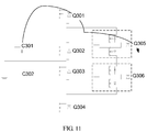
- the two direct current power supplies are a first direct current power supply C301 and a second direct current power supply C302 respectively.
- the four power frequency rectifier transistors are a first power frequency rectifier transistor Q301, a second power frequency rectifier transistor Q302, a third power frequency rectifier transistor Q303, and a fourth power frequency rectifier transistor Q304 respectively.
- the two equivalent transistors are a first equivalent transistor Q305 and a second equivalent transistor Q306 respectively.
- a first end of the first power frequency rectifier transistor Q301 is electrically connected to a first end of the first direct current power supply C301.
- a second end of the first power frequency rectifier transistor Q301 is electrically connected to a first end of the second power frequency rectifier transistor Q302.
- a second end of the second power frequency rectifier transistor Q302 is electrically connected to a second end of the first direct current power supply C301.
- a first end of the third power frequency rectifier transistor Q303 is electrically connected to a first end of the second direct current power supply C302.
- a second end of the third power frequency rectifier transistor Q303 is electrically connected to a first end of the fourth power frequency rectifier transistor Q304.
- a second end of the fourth power frequency rectifier transistor Q304 is electrically connected to a second end of the second direct current power supply C302.
- the second end of the second power frequency rectifier transistor Q302, the second end of the first direct current power supply C301, the first end of the third power frequency rectifier transistor Q303, and the first end of the second direct current power supply C302 are electrically connected and grounded.
- a second end of the first equivalent transistor Q305 is electrically connected to a first end of the second equivalent transistor Q306.
- a first end of the first equivalent transistor Q305, the second end of the first power frequency rectifier transistor Q301, and the first end of the second power frequency rectifier transistor Q302 are electrically connected.
- a second end of the second equivalent transistor Q306, the second end of the third power frequency rectifier transistor Q303, and the first end of the fourth power frequency rectifier transistor Q304 are electrically connected.
- a connection end of the first equivalent transistor Q305 and the second equivalent transistor Q306 is an output end of the three-level inverter.
- the power frequency rectifier transistor is a transistor that can convert an alternating current whose direction alternately changes into a direct current that has a single direction.
- capacitors C301 and C302 are direct current supplies, and provide direct current voltages of -U/2 to +U/2.
- Transistors Q301, Q302, Q303, and Q304 are power frequency rectifier transistors, and are connected in series between positive electrodes and negative electrodes of direct current power supplies. There is an electric potential of 0 between Q302 and Q303.
- the equivalent transistors Q305 and Q306 are connected in series, and a branch circuit is connected in parallel to Q302 and Q303.
- a connection end of Q305 and Q306 is an output end of the three-level inverter.
- all of the four power frequency rectifier transistors are IGBTs (Insulated Gate Bipolar Transistor, insulated gate bipolar transistor).
- the first power frequency rectifier transistor Q301, the second power frequency rectifier transistor Q302, the third power frequency rectifier transistor Q303, and the fourth power frequency rectifier transistor Q304 in an output positive half cycle of the three-level inverter, the first power frequency rectifier transistor Q301 and the third power frequency rectifier transistor Q303 are conducted, and the second power frequency rectifier transistor Q302 and the fourth power frequency rectifier transistor Q304 are cut off; and in an output negative half cycle of the three-level inverter, the first power frequency rectifier transistor Q301 and the third power frequency rectifier transistor Q303 are cut off, and the second power frequency rectifier transistor Q302 and the fourth power frequency rectifier transistor Q304 are conducted.
- the first equivalent transistor Q305 and the second equivalent transistor Q306 are complementarily conducted, and a switching cycle of complementary conduction is less than an output cycle of the three-level inverter.
- the output positive half cycle and the output negative half cycle are respectively a positive half cycle and a negative half cycle of an alternating current output by the three-level inverter.
- the switching cycle is a period in which Q305 or Q306 is conducted, cut off, and then conducted again, and a length of the switching cycle continuously changes sinusoidally.
- the output cycle is a change cycle of the alternating current output by the three-level inverter.
- FIG. 10 is a schematic diagram of a current when Q301 and Q305 are conducted in the positive half cycle, and a direction of the current is from C301 to Q301 and then to Q305.
- FIG. 11 is a schematic diagram of a current when Q301 and Q305 are conducted in the positive half cycle, and a direction of the current is from C301 to Q301 and then to Q305.
- FIG. 12 is a schematic diagram of a current when Q303 and Q306 are conducted in the positive half cycle, and a direction of the current is from a ground terminal to Q303 and then to Q306, or is from Q306 to Q303 and then to a ground terminal.
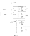
- FIG. 13 is a schematic diagram of a current when Q302 and Q305 are conducted in the negative half cycle, and a direction of the current is from a ground terminal to Q302 and then to Q305, or is from Q305 to Q302 and then to a ground terminal.
- FIG. 14 is a schematic diagram of a current when Q304 and Q306 are conducted in the negative half cycle, and a direction of the current is from Q306 to Q304 and then to C302.
- the three-level inverter further includes at least one equivalent transistor group G.
- Each equivalent transistor group G includes two equivalent transistors that are connected in series.
- a branch circuit formed by connecting the two equivalent transistors in series is connected in parallel to branch circuits of the first equivalent transistor Q305 and the second equivalent transistor Q306.
- a connection end of the two equivalent transistors in each equivalent transistor group is an output end of the three-level inverter.
- a circuit structure of the three-level inverter may further include the at least one equivalent transistor group G.
- each equivalent transistor group G includes the two equivalent transistors that are connected in series.
- the branch circuit formed by connecting the two equivalent transistors in series is connected in parallel to the branch circuits of the first equivalent transistor Q305 and the second equivalent transistor Q306.
- the connection end of the two equivalent transistors in each equivalent transistor group is the output end of the three-level inverter. It is easily understood that Q305 and Q306 form an equivalent transistor group G, and in addition to different phases, control signals of all equivalent transistor groups may have the same other parameters.
- each output end may be connected to an LC filter. Filtered output voltages may form an alternating current with a higher frequency after being coupled in a staggered manner.
- an equivalent transistor includes a first transistor, a second transistor, and a diode.
- a source electrode of the first transistor is electrically connected to a source electrode of the second transistor; a gate electrode of the first transistor is electrically connected to a gate electrode of the second transistor; and one end of the diode is electrically connected to a drain electrode of the first transistor, and the other end of the diode is electrically connected to a drain electrode of the second transistor.
- the diode is a separate diode, and a diode with a relatively good reverse recovery feature may be used.
- a current cannot flow through parasitic diodes of the first transistor and the second transistor, but flows through the diode with the relatively good reverse recovery feature. Therefore, a reverse recovery time can be reduced, and a switching speed of the equivalent transistor can increase.
Landscapes
- Engineering & Computer Science (AREA)
- Power Engineering (AREA)
- Inverter Devices (AREA)
- Electronic Switches (AREA)
Claims (4)
- Onduleur à trois niveaux, l'onduleur à trois niveaux comprenant deux alimentations électriques en courant continu (C301, C302), des transistors redresseurs de fréquence de régime (Q301, Q302, Q303, Q304), un premier transistor équivalent (Q305) et un second transistor équivalent (Q306),
dans lequel chacun des deux transistors équivalents (Q305, Q306) comprend un premier transistor (T101), un second transistor (T102), et une diode (D101) ; une électrode de source du premier transistor (T101) est connectée électriquement à une électrode de source du second transistor (T102) ; une électrode de grille du premier transistor (T101) est connectée électriquement à une électrode de grille du second transistor (T102) ; et une extrémité de la diode (D101) est connectée électriquement à une extrémité de drain du premier transistor (T101), et l'autre extrémité de la diode (D101) est connectée électriquement à une électrode de drain du second transistor (T102) dans lequel
une extrémité de connexion du premier transistor équivalent (Q305) et du second transistor équivalent (Q306) est une extrémité de sortie de l'onduleur à trois niveaux, dans lequel les deux alimentations électriques en courant continu (C301, C302) sont une première alimentation électrique en courant continu (C301) et une seconde alimentation électrique en courant continu (C302) respectivement,
dans lequel les transistors redresseurs de fréquence de régime (Q301, Q302, Q303, Q304) comprennent un premier transistor redresseur de fréquence de régime (Q301) et un deuxième transistor redresseur de fréquence de régime (Q302),
dans lequel une seconde extrémité du premier transistor redresseur de fréquence de régime (Q301) est connectée électriquement à une première extrémité du deuxième transistor redresseur de fréquence de régime (Q302), et
dans lequel une seconde extrémité de la première alimentation électrique en courant continu (C301) et une première extrémité de la seconde alimentation électrique en courant continu (C302) sont connectées électriquement et mises à la masse ; caractérisé en ce que
l'onduleur à trois niveaux comprend en outre :un troisième transistor redresseur de fréquence de régime (Q303), et un quatrième transistor redresseur de fréquence de régime (Q304) ; etune première extrémité du premier transistor redresseur de fréquence de régime (Q301) est connectée électriquement à une première extrémité de la première alimentation électrique en courant continu (C301), une seconde extrémité du deuxième transistor redresseur de fréquence de régime (Q302) est connectée électriquement à la seconde extrémité de la première alimentation électrique en courant continu (C301), une première extrémité du troisième transistor redresseur de fréquence de régime (Q303) est connectée électriquement à la première extrémité de la seconde alimentation électrique en courant continu (C302), une seconde extrémité du troisième transistor redresseur de fréquence de régime (Q303) est connectée électriquement à une première extrémité du quatrième transistor redresseur de fréquence de régime (Q304), et une seconde extrémité du quatrième transistor redresseur de fréquence de régime (Q304) est connectée électriquement à une seconde extrémité de la seconde alimentation électrique en courant continu (C302) ;dans lequel une seconde extrémité du premier transistor équivalent (Q305) est connectée électriquement à une première extrémité du second transistor équivalent (Q306), une première extrémité du premier transistor équivalent (Q305), la seconde extrémité du premier transistor redresseur de fréquence de régime (Q301), et la première extrémité du deuxième transistor redresseur de fréquence de régime (Q302) sont connectées électriquement, et une seconde extrémité du second transistor équivalent (Q306), la seconde extrémité du troisième transistor redresseur de fréquence de régime (Q303), et la première extrémité du quatrième transistor redresseur de fréquence de régime (Q304) sont connectées électriquement. - Onduleur à trois niveaux selon la revendication 1, dans lequel la totalité des quatre transistors redresseurs de fréquence de régime (Q301, Q302, Q303, Q304) sont des IGBT.
- Onduleur à trois niveaux selon la revendication 1, dans lequel sur la base de signaux de commande du premier transistor redresseur de fréquence de régime (Q301), du deuxième transistor redresseur de fréquence de régime (Q302), du troisième transistor redresseur de fréquence de régime (Q303), et du quatrième transistor redresseur de fréquence de régime (Q304), dans une alternance positive de sortie de l'onduleur à trois niveaux, le premier transistor redresseur de fréquence de régime (Q301) et le troisième transistor redresseur de fréquence de régime (Q303) conduisent, et le deuxième transistor redresseur de fréquence de régime (Q302) et le quatrième transistor redresseur de fréquence de régime (Q304) sont coupés : et dans une alternance négative de sortie de l'onduleur à trois niveaux, le premier transistor redresseur de fréquence de régime (Q301) et le troisième transistor redresseur de fréquence de régime (Q303) sont coupés, et le deuxième transistor redresseur de fréquence de régime (Q302) et le quatrième transistor redresseur de fréquence de régime (Q304) conduisent ; et
sur la base de signaux de commande du premier transistor équivalent (Q305) et du second transistor équivalent (Q306), le premier transistor équivalent (Q305) et le second transistor équivalent (Q306) conduisent de manière complémentaire, et un cycle de commutation de conduction complémentaire est plus court qu'un cycle de sortie de l'onduleur à trois niveaux. - Onduleur à trois niveaux selon la revendication 1, l'onduleur à trois niveaux comprenant en outre au moins un groupe de transistors équivalents, chaque groupe de transistors équivalents comprenant deux transistors équivalents qui sont connectés en série, un circuit de dérivation formé en connectant les deux transistors équivalents (Q305, Q306) en série est connecté en parallèle à des circuits de dérivation du premier transistor équivalent (Q305) et du second transistor équivalent (Q306), et une extrémité de connexion des deux transistors équivalents (Q305, Q306) dans chaque groupe de transistors équivalents est une extrémité de sortie de l'onduleur à trois niveaux.
Applications Claiming Priority (2)
| Application Number | Priority Date | Filing Date | Title |
|---|---|---|---|
| CN201510981520.XA CN105553318B (zh) | 2015-12-23 | 2015-12-23 | 一种等效晶体管和三电平逆变器 |
| PCT/CN2016/111373 WO2017107931A1 (fr) | 2015-12-23 | 2016-12-21 | Transistor équivalent et onduleur à trois niveaux |
Publications (3)
| Publication Number | Publication Date |
|---|---|
| EP3382881A1 EP3382881A1 (fr) | 2018-10-03 |
| EP3382881A4 EP3382881A4 (fr) | 2018-11-21 |
| EP3382881B1 true EP3382881B1 (fr) | 2021-06-16 |
Family
ID=55832302
Family Applications (1)
| Application Number | Title | Priority Date | Filing Date |
|---|---|---|---|
| EP16877741.5A Active EP3382881B1 (fr) | 2015-12-23 | 2016-12-21 | Transistor équivalent et onduleur à trois niveaux |
Country Status (5)
| Country | Link |
|---|---|
| US (1) | US10333427B2 (fr) |
| EP (1) | EP3382881B1 (fr) |
| CN (1) | CN105553318B (fr) |
| MY (1) | MY195940A (fr) |
| WO (1) | WO2017107931A1 (fr) |
Families Citing this family (8)
| Publication number | Priority date | Publication date | Assignee | Title |
|---|---|---|---|---|
| CN105553318B (zh) * | 2015-12-23 | 2020-04-21 | 华为技术有限公司 | 一种等效晶体管和三电平逆变器 |
| US10230364B2 (en) * | 2017-04-26 | 2019-03-12 | Futurewei Technologies, Inc. | Hybrid power devices |
| US10608624B2 (en) * | 2017-05-25 | 2020-03-31 | Solaredge Technologies Ltd. | Efficient switching circuit |
| CN108390581A (zh) * | 2018-02-09 | 2018-08-10 | 华为技术有限公司 | 一种用于逆变器或整流器的电桥电路 |
| CN110649831B (zh) * | 2019-05-10 | 2021-04-13 | 阳光电源股份有限公司 | 多电平逆变电路的关机封波控制方法及其应用装置 |
| CN114024462B (zh) * | 2021-12-03 | 2025-12-26 | 上海安世博能源科技有限公司 | 三电平控制电路、功率变换装置及其控制方法 |
| CN114336873B (zh) | 2021-12-29 | 2026-01-30 | 上海安世博能源科技有限公司 | 功率控制电路及其控制方法 |
| CN114301303B (zh) | 2021-12-29 | 2026-01-16 | 上海安世博能源科技有限公司 | 电路控制方法及其装置 |
Family Cites Families (19)
| Publication number | Priority date | Publication date | Assignee | Title |
|---|---|---|---|---|
| JPH05211776A (ja) * | 1992-01-31 | 1993-08-20 | Fuji Electric Co Ltd | インバータ |
| DE50110556D1 (de) * | 2000-09-13 | 2006-09-07 | Abb Research Ltd | Steuer- und regelverfahren für einen dreipunkt-stromrichter mit aktiven klemmschaltern sowie vorrichtung hierzu |
| US6838925B1 (en) * | 2003-10-07 | 2005-01-04 | American Power Conversion Corporation | Three level inverter |
| US7995362B2 (en) * | 2005-06-15 | 2011-08-09 | Ameritherm, Inc. | High voltage full bridge circuit and method for operating the same |
| CN101523614B (zh) * | 2006-11-20 | 2011-04-20 | 松下电器产业株式会社 | 半导体装置及其驱动方法 |
| US8582331B2 (en) * | 2009-07-20 | 2013-11-12 | Vincotech Holdings S.à.r.l. | Inverter topologies usable with reactive power |
| EP2413489B1 (fr) * | 2010-07-30 | 2013-09-11 | Vinotech Holdings S.à.r.l. | Convertisseur courant continu courant alternatif à demi-pont hautement efficace |
| US8929114B2 (en) * | 2011-02-24 | 2015-01-06 | Virginia Tech Intellectual Properties, Inc. | Three-level active neutral point clamped zero voltage switching converter |
| EP2590312A1 (fr) * | 2011-11-04 | 2013-05-08 | Alstom Technology Ltd | Convertisseur de source de tension avec topologie clampée en neutre modifiée et procédé de fonctionnement d'un tel convertisseur |
| CN102611342B (zh) | 2012-03-13 | 2014-10-08 | 华为技术有限公司 | 三电平逆变器 |
| CN103312202B (zh) * | 2012-03-14 | 2016-05-04 | 山特电子(深圳)有限公司 | 高频应用中的逆变器拓扑及其控制方法 |
| CN102946205A (zh) * | 2012-10-29 | 2013-02-27 | 华为技术有限公司 | 三电平逆变器和供电设备 |
| JP6184107B2 (ja) * | 2013-01-29 | 2017-08-23 | 株式会社東芝 | 中性点クランプ式電力変換装置 |
| CN103475248B (zh) * | 2013-08-30 | 2016-12-07 | 华为技术有限公司 | 功率变换电路和功率变换系统 |
| US9397584B2 (en) * | 2013-09-25 | 2016-07-19 | Eaton Corporation | Multi-level converter apparatus and methods using clamped node bias |
| EP2871765A1 (fr) * | 2013-11-08 | 2015-05-13 | Vincotech GmbH | Convertisseur NPC destiné à être utilisé dans un module de puissance et ledit module incorporant celui-ci |
| JPWO2015079762A1 (ja) * | 2013-11-29 | 2017-03-16 | シャープ株式会社 | 整流装置 |
| US9716444B2 (en) * | 2015-11-05 | 2017-07-25 | Ge Energy Power Conversion Technology Ltd | Pulse width modulation (PWM) for multi-level power inverters |
| CN105553318B (zh) * | 2015-12-23 | 2020-04-21 | 华为技术有限公司 | 一种等效晶体管和三电平逆变器 |
-
2015
- 2015-12-23 CN CN201510981520.XA patent/CN105553318B/zh active Active
-
2016
- 2016-12-21 WO PCT/CN2016/111373 patent/WO2017107931A1/fr not_active Ceased
- 2016-12-21 MY MYPI2018001037A patent/MY195940A/en unknown
- 2016-12-21 EP EP16877741.5A patent/EP3382881B1/fr active Active
-
2018
- 2018-06-22 US US16/015,217 patent/US10333427B2/en active Active
Also Published As
| Publication number | Publication date |
|---|---|
| US20180302005A1 (en) | 2018-10-18 |
| CN105553318B (zh) | 2020-04-21 |
| EP3382881A1 (fr) | 2018-10-03 |
| EP3382881A4 (fr) | 2018-11-21 |
| WO2017107931A1 (fr) | 2017-06-29 |
| MY195940A (en) | 2023-02-27 |
| US10333427B2 (en) | 2019-06-25 |
| CN105553318A (zh) | 2016-05-04 |
Similar Documents
| Publication | Publication Date | Title |
|---|---|---|
| EP3382881B1 (fr) | Transistor équivalent et onduleur à trois niveaux | |
| TWI505626B (zh) | Semiconductor switch and power conversion device | |
| US20130214824A1 (en) | Driving circuit | |
| US9356516B2 (en) | Driving apparatus and electric power converter | |
| US9450517B2 (en) | Driving apparatus and electric power converter | |
| US8120391B2 (en) | Circuit arrangement including a voltage supply circuit and semiconductor switching element | |
| US8916882B2 (en) | Switching circuit and semiconductor module | |
| JP5845428B2 (ja) | 駆動装置、電力変換装置、車両 | |
| US10581342B2 (en) | Three-level two-stage decoupled active NPC converter | |
| CN101632214A (zh) | 半导体开关和配备半导体开关的功率转换系统 | |
| EP2871765A1 (fr) | Convertisseur NPC destiné à être utilisé dans un module de puissance et ledit module incorporant celui-ci | |
| JP5619673B2 (ja) | スイッチング回路及び半導体モジュール | |
| JP2018011404A (ja) | 駆動対象スイッチの駆動回路 | |
| CN107787548A (zh) | 充电共用逆变器 | |
| WO2021169244A1 (fr) | Circuit de commande de convertisseur à trois niveaux de type npc, convertisseur à trois niveaux de type npc et ensemble générateur d'énergie éolienne | |
| JP3900178B2 (ja) | レベルシフト回路 | |
| CN110970882A (zh) | 一种保护电路及电池管理系统 | |
| JP6338145B2 (ja) | 半導体装置及びそれを用いた電力変換装置 | |
| JP6939087B2 (ja) | 集積回路装置 | |
| JP5594263B2 (ja) | ハーフブリッジ回路 | |
| JP2015156795A (ja) | 半導体スイッチ回路および電力変換装置 | |
| US9276476B1 (en) | Forced commutating a current through a diode | |
| RU148939U1 (ru) | Силовое полупроводниковое устройство с обратным диодом | |
| WO2019039064A1 (fr) | Circuit de conversion de puissance à semi-conducteur et dispositif à semi-conducteur ainsi que dispositif de pilotage de moteur l'utilisant | |
| CN105846413B (zh) | 高电压抑制方法及装置 |
Legal Events
| Date | Code | Title | Description |
|---|---|---|---|
| STAA | Information on the status of an ep patent application or granted ep patent |
Free format text: STATUS: THE INTERNATIONAL PUBLICATION HAS BEEN MADE |
|
| PUAI | Public reference made under article 153(3) epc to a published international application that has entered the european phase |
Free format text: ORIGINAL CODE: 0009012 |
|
| STAA | Information on the status of an ep patent application or granted ep patent |
Free format text: STATUS: REQUEST FOR EXAMINATION WAS MADE |
|
| 17P | Request for examination filed |
Effective date: 20180626 |
|
| AK | Designated contracting states |
Kind code of ref document: A1 Designated state(s): AL AT BE BG CH CY CZ DE DK EE ES FI FR GB GR HR HU IE IS IT LI LT LU LV MC MK MT NL NO PL PT RO RS SE SI SK SM TR |
|
| AX | Request for extension of the european patent |
Extension state: BA ME |
|
| A4 | Supplementary search report drawn up and despatched |
Effective date: 20181019 |
|
| RIC1 | Information provided on ipc code assigned before grant |
Ipc: H02M 7/487 20070101AFI20181015BHEP Ipc: H02M 1/00 20060101ALI20181015BHEP |
|
| DAV | Request for validation of the european patent (deleted) | ||
| DAX | Request for extension of the european patent (deleted) | ||
| RIC1 | Information provided on ipc code assigned before grant |
Ipc: H02M 7/487 20070101AFI20201201BHEP Ipc: H02M 1/00 20060101ALI20201201BHEP |
|
| GRAP | Despatch of communication of intention to grant a patent |
Free format text: ORIGINAL CODE: EPIDOSNIGR1 |
|
| STAA | Information on the status of an ep patent application or granted ep patent |
Free format text: STATUS: GRANT OF PATENT IS INTENDED |
|
| INTG | Intention to grant announced |
Effective date: 20210122 |
|
| GRAS | Grant fee paid |
Free format text: ORIGINAL CODE: EPIDOSNIGR3 |
|
| GRAA | (expected) grant |
Free format text: ORIGINAL CODE: 0009210 |
|
| STAA | Information on the status of an ep patent application or granted ep patent |
Free format text: STATUS: THE PATENT HAS BEEN GRANTED |
|
| AK | Designated contracting states |
Kind code of ref document: B1 Designated state(s): AL AT BE BG CH CY CZ DE DK EE ES FI FR GB GR HR HU IE IS IT LI LT LU LV MC MK MT NL NO PL PT RO RS SE SI SK SM TR |
|
| REG | Reference to a national code |
Ref country code: GB Ref legal event code: FG4D |
|
| REG | Reference to a national code |
Ref country code: CH Ref legal event code: EP |
|
| REG | Reference to a national code |
Ref country code: DE Ref legal event code: R096 Ref document number: 602016059516 Country of ref document: DE |
|
| REG | Reference to a national code |
Ref country code: AT Ref legal event code: REF Ref document number: 1403173 Country of ref document: AT Kind code of ref document: T Effective date: 20210715 |
|
| REG | Reference to a national code |
Ref country code: IE Ref legal event code: FG4D |
|
| REG | Reference to a national code |
Ref country code: LT Ref legal event code: MG9D |
|
| PG25 | Lapsed in a contracting state [announced via postgrant information from national office to epo] |
Ref country code: BG Free format text: LAPSE BECAUSE OF FAILURE TO SUBMIT A TRANSLATION OF THE DESCRIPTION OR TO PAY THE FEE WITHIN THE PRESCRIBED TIME-LIMIT Effective date: 20210916 Ref country code: HR Free format text: LAPSE BECAUSE OF FAILURE TO SUBMIT A TRANSLATION OF THE DESCRIPTION OR TO PAY THE FEE WITHIN THE PRESCRIBED TIME-LIMIT Effective date: 20210616 Ref country code: FI Free format text: LAPSE BECAUSE OF FAILURE TO SUBMIT A TRANSLATION OF THE DESCRIPTION OR TO PAY THE FEE WITHIN THE PRESCRIBED TIME-LIMIT Effective date: 20210616 Ref country code: LT Free format text: LAPSE BECAUSE OF FAILURE TO SUBMIT A TRANSLATION OF THE DESCRIPTION OR TO PAY THE FEE WITHIN THE PRESCRIBED TIME-LIMIT Effective date: 20210616 |
|
| REG | Reference to a national code |
Ref country code: AT Ref legal event code: MK05 Ref document number: 1403173 Country of ref document: AT Kind code of ref document: T Effective date: 20210616 |
|
| REG | Reference to a national code |
Ref country code: NL Ref legal event code: MP Effective date: 20210616 |
|
| PG25 | Lapsed in a contracting state [announced via postgrant information from national office to epo] |
Ref country code: RS Free format text: LAPSE BECAUSE OF FAILURE TO SUBMIT A TRANSLATION OF THE DESCRIPTION OR TO PAY THE FEE WITHIN THE PRESCRIBED TIME-LIMIT Effective date: 20210616 Ref country code: SE Free format text: LAPSE BECAUSE OF FAILURE TO SUBMIT A TRANSLATION OF THE DESCRIPTION OR TO PAY THE FEE WITHIN THE PRESCRIBED TIME-LIMIT Effective date: 20210616 Ref country code: NO Free format text: LAPSE BECAUSE OF FAILURE TO SUBMIT A TRANSLATION OF THE DESCRIPTION OR TO PAY THE FEE WITHIN THE PRESCRIBED TIME-LIMIT Effective date: 20210916 Ref country code: LV Free format text: LAPSE BECAUSE OF FAILURE TO SUBMIT A TRANSLATION OF THE DESCRIPTION OR TO PAY THE FEE WITHIN THE PRESCRIBED TIME-LIMIT Effective date: 20210616 Ref country code: GR Free format text: LAPSE BECAUSE OF FAILURE TO SUBMIT A TRANSLATION OF THE DESCRIPTION OR TO PAY THE FEE WITHIN THE PRESCRIBED TIME-LIMIT Effective date: 20210917 |
|
| RAP2 | Party data changed (patent owner data changed or rights of a patent transferred) |
Owner name: HUAWEI DIGITAL POWER TECHNOLOGIES CO., LTD. |
|
| REG | Reference to a national code |
Ref country code: DE Ref legal event code: R081 Ref document number: 602016059516 Country of ref document: DE Owner name: HUAWEI DIGITAL POWER TECHNOLOGIES CO., LTD., S, CN Free format text: FORMER OWNER: HUAWEI TECHNOLOGIES CO., LTD., SHENZHEN, GUANGDONG, CN |
|
| PG25 | Lapsed in a contracting state [announced via postgrant information from national office to epo] |
Ref country code: AT Free format text: LAPSE BECAUSE OF FAILURE TO SUBMIT A TRANSLATION OF THE DESCRIPTION OR TO PAY THE FEE WITHIN THE PRESCRIBED TIME-LIMIT Effective date: 20210616 Ref country code: CZ Free format text: LAPSE BECAUSE OF FAILURE TO SUBMIT A TRANSLATION OF THE DESCRIPTION OR TO PAY THE FEE WITHIN THE PRESCRIBED TIME-LIMIT Effective date: 20210616 Ref country code: EE Free format text: LAPSE BECAUSE OF FAILURE TO SUBMIT A TRANSLATION OF THE DESCRIPTION OR TO PAY THE FEE WITHIN THE PRESCRIBED TIME-LIMIT Effective date: 20210616 Ref country code: ES Free format text: LAPSE BECAUSE OF FAILURE TO SUBMIT A TRANSLATION OF THE DESCRIPTION OR TO PAY THE FEE WITHIN THE PRESCRIBED TIME-LIMIT Effective date: 20210616 Ref country code: NL Free format text: LAPSE BECAUSE OF FAILURE TO SUBMIT A TRANSLATION OF THE DESCRIPTION OR TO PAY THE FEE WITHIN THE PRESCRIBED TIME-LIMIT Effective date: 20210616 Ref country code: PT Free format text: LAPSE BECAUSE OF FAILURE TO SUBMIT A TRANSLATION OF THE DESCRIPTION OR TO PAY THE FEE WITHIN THE PRESCRIBED TIME-LIMIT Effective date: 20211018 Ref country code: RO Free format text: LAPSE BECAUSE OF FAILURE TO SUBMIT A TRANSLATION OF THE DESCRIPTION OR TO PAY THE FEE WITHIN THE PRESCRIBED TIME-LIMIT Effective date: 20210616 Ref country code: SK Free format text: LAPSE BECAUSE OF FAILURE TO SUBMIT A TRANSLATION OF THE DESCRIPTION OR TO PAY THE FEE WITHIN THE PRESCRIBED TIME-LIMIT Effective date: 20210616 Ref country code: SM Free format text: LAPSE BECAUSE OF FAILURE TO SUBMIT A TRANSLATION OF THE DESCRIPTION OR TO PAY THE FEE WITHIN THE PRESCRIBED TIME-LIMIT Effective date: 20210616 |
|
| PG25 | Lapsed in a contracting state [announced via postgrant information from national office to epo] |
Ref country code: PL Free format text: LAPSE BECAUSE OF FAILURE TO SUBMIT A TRANSLATION OF THE DESCRIPTION OR TO PAY THE FEE WITHIN THE PRESCRIBED TIME-LIMIT Effective date: 20210616 |
|
| REG | Reference to a national code |
Ref country code: DE Ref legal event code: R097 Ref document number: 602016059516 Country of ref document: DE |
|
| PLBE | No opposition filed within time limit |
Free format text: ORIGINAL CODE: 0009261 |
|
| STAA | Information on the status of an ep patent application or granted ep patent |
Free format text: STATUS: NO OPPOSITION FILED WITHIN TIME LIMIT |
|
| PG25 | Lapsed in a contracting state [announced via postgrant information from national office to epo] |
Ref country code: DK Free format text: LAPSE BECAUSE OF FAILURE TO SUBMIT A TRANSLATION OF THE DESCRIPTION OR TO PAY THE FEE WITHIN THE PRESCRIBED TIME-LIMIT Effective date: 20210616 |
|
| 26N | No opposition filed |
Effective date: 20220317 |
|
| PG25 | Lapsed in a contracting state [announced via postgrant information from national office to epo] |
Ref country code: AL Free format text: LAPSE BECAUSE OF FAILURE TO SUBMIT A TRANSLATION OF THE DESCRIPTION OR TO PAY THE FEE WITHIN THE PRESCRIBED TIME-LIMIT Effective date: 20210616 |
|
| PG25 | Lapsed in a contracting state [announced via postgrant information from national office to epo] |
Ref country code: MC Free format text: LAPSE BECAUSE OF FAILURE TO SUBMIT A TRANSLATION OF THE DESCRIPTION OR TO PAY THE FEE WITHIN THE PRESCRIBED TIME-LIMIT Effective date: 20210616 Ref country code: IT Free format text: LAPSE BECAUSE OF FAILURE TO SUBMIT A TRANSLATION OF THE DESCRIPTION OR TO PAY THE FEE WITHIN THE PRESCRIBED TIME-LIMIT Effective date: 20210616 |
|
| REG | Reference to a national code |
Ref country code: CH Ref legal event code: PL |
|
| GBPC | Gb: european patent ceased through non-payment of renewal fee |
Effective date: 20211221 |
|
| REG | Reference to a national code |
Ref country code: BE Ref legal event code: MM Effective date: 20211231 |
|
| PG25 | Lapsed in a contracting state [announced via postgrant information from national office to epo] |
Ref country code: LU Free format text: LAPSE BECAUSE OF NON-PAYMENT OF DUE FEES Effective date: 20211221 Ref country code: IE Free format text: LAPSE BECAUSE OF NON-PAYMENT OF DUE FEES Effective date: 20211221 Ref country code: GB Free format text: LAPSE BECAUSE OF NON-PAYMENT OF DUE FEES Effective date: 20211221 |
|
| PG25 | Lapsed in a contracting state [announced via postgrant information from national office to epo] |
Ref country code: BE Free format text: LAPSE BECAUSE OF NON-PAYMENT OF DUE FEES Effective date: 20211231 |
|
| PG25 | Lapsed in a contracting state [announced via postgrant information from national office to epo] |
Ref country code: LI Free format text: LAPSE BECAUSE OF NON-PAYMENT OF DUE FEES Effective date: 20211231 Ref country code: CH Free format text: LAPSE BECAUSE OF NON-PAYMENT OF DUE FEES Effective date: 20211231 |
|
| PG25 | Lapsed in a contracting state [announced via postgrant information from national office to epo] |
Ref country code: HU Free format text: LAPSE BECAUSE OF FAILURE TO SUBMIT A TRANSLATION OF THE DESCRIPTION OR TO PAY THE FEE WITHIN THE PRESCRIBED TIME-LIMIT; INVALID AB INITIO Effective date: 20161221 |
|
| P01 | Opt-out of the competence of the unified patent court (upc) registered |
Effective date: 20230524 |
|
| PG25 | Lapsed in a contracting state [announced via postgrant information from national office to epo] |
Ref country code: CY Free format text: LAPSE BECAUSE OF FAILURE TO SUBMIT A TRANSLATION OF THE DESCRIPTION OR TO PAY THE FEE WITHIN THE PRESCRIBED TIME-LIMIT Effective date: 20210616 |
|
| PG25 | Lapsed in a contracting state [announced via postgrant information from national office to epo] |
Ref country code: MK Free format text: LAPSE BECAUSE OF FAILURE TO SUBMIT A TRANSLATION OF THE DESCRIPTION OR TO PAY THE FEE WITHIN THE PRESCRIBED TIME-LIMIT Effective date: 20210616 |
|
| PG25 | Lapsed in a contracting state [announced via postgrant information from national office to epo] |
Ref country code: TR Free format text: LAPSE BECAUSE OF FAILURE TO SUBMIT A TRANSLATION OF THE DESCRIPTION OR TO PAY THE FEE WITHIN THE PRESCRIBED TIME-LIMIT Effective date: 20210616 |
|
| PG25 | Lapsed in a contracting state [announced via postgrant information from national office to epo] |
Ref country code: MT Free format text: LAPSE BECAUSE OF FAILURE TO SUBMIT A TRANSLATION OF THE DESCRIPTION OR TO PAY THE FEE WITHIN THE PRESCRIBED TIME-LIMIT Effective date: 20210616 |
|
| PGFP | Annual fee paid to national office [announced via postgrant information from national office to epo] |
Ref country code: DE Payment date: 20251104 Year of fee payment: 10 |
|
| PGFP | Annual fee paid to national office [announced via postgrant information from national office to epo] |
Ref country code: FR Payment date: 20251110 Year of fee payment: 10 |