EP3385687A1 - Dispositif optique de mesure - Google Patents
Dispositif optique de mesure Download PDFInfo
- Publication number
- EP3385687A1 EP3385687A1 EP16870499.7A EP16870499A EP3385687A1 EP 3385687 A1 EP3385687 A1 EP 3385687A1 EP 16870499 A EP16870499 A EP 16870499A EP 3385687 A1 EP3385687 A1 EP 3385687A1
- Authority
- EP
- European Patent Office
- Prior art keywords
- optical
- measurement
- optical fiber
- optical device
- electronic component
- Prior art date
- Legal status (The legal status is an assumption and is not a legal conclusion. Google has not performed a legal analysis and makes no representation as to the accuracy of the status listed.)
- Granted
Links
Images


Classifications
-
- G—PHYSICS
- G01—MEASURING; TESTING
- G01J—MEASUREMENT OF INTENSITY, VELOCITY, SPECTRAL CONTENT, POLARISATION, PHASE OR PULSE CHARACTERISTICS OF INFRARED, VISIBLE OR ULTRAVIOLET LIGHT; COLORIMETRY; RADIATION PYROMETRY
- G01J3/00—Spectrometry; Spectrophotometry; Monochromators; Measuring colours
- G01J3/02—Details
- G01J3/0286—Constructional arrangements for compensating for fluctuations caused by temperature, humidity or pressure, or using cooling or temperature stabilization of parts of the device; Controlling the atmosphere inside a spectrometer, e.g. vacuum
-
- G—PHYSICS
- G01—MEASURING; TESTING
- G01J—MEASUREMENT OF INTENSITY, VELOCITY, SPECTRAL CONTENT, POLARISATION, PHASE OR PULSE CHARACTERISTICS OF INFRARED, VISIBLE OR ULTRAVIOLET LIGHT; COLORIMETRY; RADIATION PYROMETRY
- G01J1/00—Photometry, e.g. photographic exposure meter
- G01J1/02—Details
-
- G—PHYSICS
- G01—MEASURING; TESTING
- G01J—MEASUREMENT OF INTENSITY, VELOCITY, SPECTRAL CONTENT, POLARISATION, PHASE OR PULSE CHARACTERISTICS OF INFRARED, VISIBLE OR ULTRAVIOLET LIGHT; COLORIMETRY; RADIATION PYROMETRY
- G01J1/00—Photometry, e.g. photographic exposure meter
- G01J1/02—Details
- G01J1/0204—Compact construction
-
- G—PHYSICS
- G01—MEASURING; TESTING
- G01J—MEASUREMENT OF INTENSITY, VELOCITY, SPECTRAL CONTENT, POLARISATION, PHASE OR PULSE CHARACTERISTICS OF INFRARED, VISIBLE OR ULTRAVIOLET LIGHT; COLORIMETRY; RADIATION PYROMETRY
- G01J1/00—Photometry, e.g. photographic exposure meter
- G01J1/02—Details
- G01J1/0252—Constructional arrangements for compensating for fluctuations caused by, e.g. temperature, or using cooling or temperature stabilization of parts of the device; Controlling the atmosphere inside a photometer; Purge systems, cleaning devices
-
- G—PHYSICS
- G01—MEASURING; TESTING
- G01J—MEASUREMENT OF INTENSITY, VELOCITY, SPECTRAL CONTENT, POLARISATION, PHASE OR PULSE CHARACTERISTICS OF INFRARED, VISIBLE OR ULTRAVIOLET LIGHT; COLORIMETRY; RADIATION PYROMETRY
- G01J1/00—Photometry, e.g. photographic exposure meter
- G01J1/02—Details
- G01J1/0271—Housings; Attachments or accessories for photometers
-
- G—PHYSICS
- G01—MEASURING; TESTING
- G01J—MEASUREMENT OF INTENSITY, VELOCITY, SPECTRAL CONTENT, POLARISATION, PHASE OR PULSE CHARACTERISTICS OF INFRARED, VISIBLE OR ULTRAVIOLET LIGHT; COLORIMETRY; RADIATION PYROMETRY
- G01J3/00—Spectrometry; Spectrophotometry; Monochromators; Measuring colours
- G01J3/02—Details
- G01J3/0205—Optical elements not provided otherwise, e.g. optical manifolds, diffusers, windows
- G01J3/0218—Optical elements not provided otherwise, e.g. optical manifolds, diffusers, windows using optical fibers
-
- G—PHYSICS
- G01—MEASURING; TESTING
- G01J—MEASUREMENT OF INTENSITY, VELOCITY, SPECTRAL CONTENT, POLARISATION, PHASE OR PULSE CHARACTERISTICS OF INFRARED, VISIBLE OR ULTRAVIOLET LIGHT; COLORIMETRY; RADIATION PYROMETRY
- G01J3/00—Spectrometry; Spectrophotometry; Monochromators; Measuring colours
- G01J3/02—Details
- G01J3/0256—Compact construction
-
- G—PHYSICS
- G01—MEASURING; TESTING
- G01J—MEASUREMENT OF INTENSITY, VELOCITY, SPECTRAL CONTENT, POLARISATION, PHASE OR PULSE CHARACTERISTICS OF INFRARED, VISIBLE OR ULTRAVIOLET LIGHT; COLORIMETRY; RADIATION PYROMETRY
- G01J3/00—Spectrometry; Spectrophotometry; Monochromators; Measuring colours
- G01J3/02—Details
- G01J3/0291—Housings; Spectrometer accessories; Spatial arrangement of elements, e.g. folded path arrangements
-
- G—PHYSICS
- G01—MEASURING; TESTING
- G01J—MEASUREMENT OF INTENSITY, VELOCITY, SPECTRAL CONTENT, POLARISATION, PHASE OR PULSE CHARACTERISTICS OF INFRARED, VISIBLE OR ULTRAVIOLET LIGHT; COLORIMETRY; RADIATION PYROMETRY
- G01J3/00—Spectrometry; Spectrophotometry; Monochromators; Measuring colours
- G01J3/46—Measurement of colour; Colour measuring devices, e.g. colorimeters
- G01J3/50—Measurement of colour; Colour measuring devices, e.g. colorimeters using electric radiation detectors
Definitions
- the present invention relates to an optical device for measurement.
- Japanese Laid-Open Patent Publication No. 2002-310800 discloses an optical system for measurement as well as a tristimulus photoelectric colorimeter equipped with the optical system, with the aim of accurately measuring optical characteristics of a high-directivity object even when the light intensity is extremely weak (PTD 1).
- the tristimulus photoelectric colorimeter disclosed in PTD 1 includes an objective lens having a positive power for focusing only those beams emitted at emission angle ⁇ or less among beams emitted from a region-to-be-measured of an object, an optical fiber having an entrance surface through which the focused beam from the objective lens enters, for splitting the entering beam into three beams to output the beams, and a photoreceptor sensor receiving the three beams from the optical fiber for emitting a photoreceptor signal corresponding to tristimulus values.
- PTD 1 Japanese Laid-Open Patent Publication No. 2002-310800
- the above-referenced tristimulus photoelectric colorimeter disclosed in PTD 1 is known, for example.
- Such a tristimulus photoelectric colorimeter is equipped with an optical fiber and various electronic components. Light from an object to be measured enters through an objective lens, and the optical fiber directs the light toward a photoreceptor sensor. The electronic components process a photoreceptor signal that is output from the photoreceptor sensor.
- the influence of heat from the electronic components on the optical fiber may vary in some cases. In such cases, the color measurement accuracy of the tristimulus photoelectric colorimeter may be deteriorated.
- An object of the present invention is therefore to solve the above problem and provide an optical device for measurement suppressing deterioration of the measurement accuracy due to heat generated from electronic components.
- An optical device for measurement includes: an entrance unit to allow light from an object to be measured to enter; a photoelectric converter to convert received light into an electrical signal; an optical guide to guide the light entering through the entrance unit to the photoelectric converter; and a first electronic component and a second electronic component disposed around an optical axis of the optical guide and displaced from each other in a circumferential direction.
- an optical device for measurement suppressing deterioration of the measurement accuracy due to heat generated from electronic components can be provided.
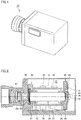
- Fig. 1 is a perspective view showing an exterior of a tristimulus photoelectric colorimeter in an embodiment of the present invention.
- Fig. 2 is a cross-sectional view showing the tristimulus photoelectric colorimeter in Fig. 1 .
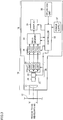
- Fig. 3 is a block diagram showing an internal configuration of the tristimulus photoelectric colorimeter in Fig. 1 .
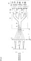
- Fig. 4 shows a specific configuration of a measurement optical system and a photoelectric converter in Fig. 2 .
- a tristimulus photoelectric colorimeter 10 (hereinafter also referred to simply as "colorimeter 10") in the present embodiment is used for example in an inspection process of a production line for liquid crystal panels, for measuring the brightness and the chromaticity of a display surface 12 of a liquid crystal panel.
- colorimeter 10 the overall configuration of colorimeter 10 is described.
- Colorimeter 10 includes a measurement probe 14 and a meter main unit 16 (see Fig. 3 ). Measurement probe 14 and meter main unit 16 are configured as an integrated unit.
- Measurement probe 14 is disposed to face display surface 12 of a liquid crystal panel to be measured, and spaced from display surface 12 by a predetermined distance (e.g., 3 cm), for example. Measurement probe 14 performs a photoelectric conversion of light from display surface 12 of the liquid crystal panel into an electrical signal (analog signal) and inputs the electrical signal to meter main unit 16.
- a predetermined distance e.g. 3 cm
- Measurement probe 14 includes a measurement optical system 27 and a photoreceptor system 28.
- Measurement optical system 27 includes an objective lens 21 and a beam splitting member 24.
- Objective lens 21 is disposed to serve as an entrance unit for allowing light from an object to be measured to enter.
- Objective lens 21 is formed for example by a plano-convex lens and has a single positive power.
- Beam splitting member 24 is disposed to serve as an optical guide for guiding the light entering through objective lens 21. Beam splitting member 24 splits the beam transmitted through objective lens 21 into three beams.
- Photoreceptor system 28 includes a photoelectric converter 25 and an amplifier 26.
- Photoelectric converter 25 receives the light guided through beam splitting member 24 for converting the light into an electrical signal.
- Photoelectric converter 25 includes photoreceptor sensors 62p, 62q, 62r having spectral sensitivity characteristics of a standard observer (see Fig. 4 ).
- Photoreceptor sensors 62p, 62q, 62r receive the three beams emitted from beam splitting member 24 for performing photoelectric conversion on the beams into electrical signals depending on the incident intensity.
- Amplifier 26 amplifies the electrical signal (voltage) output from each of photoreceptor sensors 62p, 62q, 62r to a predetermined level.
- Meter main unit 16 converts the electrical signal (analogue signal) input from measurement probe 14 into a digital signal and performs a predetermined arithmetic operation on the signal.
- Meter main unit 16 performs the arithmetic operation to thereby calculate tristimulus values (X, Y, Z), xyY (chromaticity coordinates, luminance) and T ⁇ uvY (correlated color temperature, color difference from black body locus, luminance) defined by the CIE (International Commission on Illumination), for example, and causes display 34 to show the results of the arithmetic operation.
- tristimulus values X, Y, Z
- xyY chromaticity coordinates, luminance
- T ⁇ uvY correlated color temperature, color difference from black body locus, luminance
- Beam splitting member 24 is disposed on optical axis L of light entering through objective lens 21 (also referred to simply as "optical axis of objective lens 21" hereinafter).
- Beam splitting member 24 includes an optical fiber 55 propagating light and lenses 56p, 56q, 56r having a positive power.
- Optical fiber 55 is made up of a plurality of optical fibers bundled together.
- Optical fiber 55 made up of the bundled optical fibers branches at a central portion into three so that optical fiber 55 has one beam entrance surface A and three beam emission surfaces B1, B2, B3.
- Optical fiber 55 is disposed so that beam entrance surface A is located away from image-side principal point PP of objective lens 21 by focal length f of objective lens 21 (for the sake of convenience of description, the image-side principal point coincides with the object-side principal point in the present embodiment). That is to say, objective lens 21 and optical fiber 55 constitute a telecentric optical system.
- optical fiber 55 is used for beam splitting member 24, beam splitting member 24 is not limited to such a structure.
- Other optical components performing an equivalent function to the optical fiber such as light guide may be used.
- the beams entering beam entrance surface A of optical fiber 55 are only those beams emitted at an angle smaller than or equal to maximum value ⁇ of the emission angle with respect to the normal (direction parallel to optical axis L in Fig. 4 ) to region-to-be-measured AR, among beams emitted from respective parts of region-to-be-measured AR of the liquid crystal panel.
- Maximum emission angle ⁇ is determined by focal length f of objective lens 21 and diameter R of beam entrance surface A of optical fiber 55.
- the entering beams are split in optical fiber 55 into three beams that are emitted from beam emission surfaces B1, B2, and B3, respectively.
- Each of the optical fibers constituting optical fiber 55 has a double-layer structure made up of a core located at the center and a cladding covering the periphery of the core.
- the core is designed to have a higher refractive index than the cladding. Therefore, the light is propagated in the state of being confined within the core by total reflection.
- Optical fiber 55 is disposed in a posture of being bent in a predetermined shape, while beam entrance surface A and beam emission surfaces B1, B2, B3 are fixed. Therefore, if there is no vibrational impact or state change such as temperature change, the posture of optical fiber 55 is maintained. In this case, light entering beam entrance surface A is emitted at a predetermined angle from beam emission surfaces B1, B2, B3. However, in the event of vibrational impact or state change such as temperature change, the degree of bending or posture of optical fiber 55 is changed. As a result of this, light entering beam entrance surface A will be emitted from beam emission surfaces B1, B2, B3 at an emission angle shifted from a predetermined angle.
- the angle of incidence of the light to a spectral sensitivity correction filter described later herein is shifted from a predetermined angle. Therefore, if a filter having spectral sensitivity characteristics depending on the angle of incidence is used as the spectral sensitivity correction filter, measurement data will have an error.
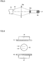
- Fig. 5 shows an irradiation range of a beam emitted from the optical fiber.
- lens 56p focuses the beam emitted from beam emission surface B1 of optical fiber 55 on photoreceptor sensor 62p so that irradiation range LA of the beam substantially matches photo-receiving range SA of photoreceptor sensor 62p.
- lens 56q focuses the beam emitted from beam emission surface B2 of optical fiber 55 on photoreceptor sensor 62q so that the irradiation range of the beam substantially matches the photo-receiving range of photoreceptor sensor 62q.
- Lens 56r focuses the beam emitted from beam emission surface B3 of optical fiber 55 on photoreceptor sensor 62r so that the irradiation range of the beam substantially matches the photo-receiving range of photoreceptor sensor 62r.
- each one-third of the beams entering optical fiber 55 (all the beams emitted from respective parts of region-to-be-measured AR of the liquid crystal panel at an emission angle less than or equal to maximum emission angle ⁇ with respect to the normal to region-to-be-measured AR) enters corresponding one of photoreceptor sensors 62p, 62q, 62r. Therefore, the amount of light received by photoreceptor sensors 62p, 62q, 62r does not decrease.
- photoelectric converter 25 further includes spectral sensitivity correction filters 61p, 61q, 61r for photoreceptor sensors 62p, 62q, 62r to have a spectral sensitivity of a standard observer defined by the CIE.
- Photoreceptor sensors 62p, 62q, 62r are formed of respective SPCs (silicon photocells) having respective photo-receiving sensitivities substantially identical to each other. Photoreceptor sensors 62p, 62q, 62r are disposed at respective positions on the optical axes of lenses 56p, 56q, 56r, respectively, so that respective irradiation ranges of the beams focused by lenses 56p, 56q, 56r match respective photo-receiving ranges of photoreceptor sensors 62p, 62q, 62r. Spectral sensitivity correction filters 61p, 61q, 61r are disposed at respective appropriate positions located between photoreceptor sensors 62p, 62q, 62r and lenses 56p, 56q, 56r.
- SPCs silicon photocells
- Spectral sensitivity correction filter 61p has a filtering characteristic exhibiting sensitivity to the R (red) wavelength range. With this filtering characteristic, the photo-receiving sensitivity of photoreceptor sensor 62p is corrected to a photo-receiving sensitivity of a matching function (x-bar ⁇ ) with a high sensitivity to the red wavelength range.
- Spectral sensitivity correction filter 61q has a filtering characteristic exhibiting sensitivity to the G (green) wavelength range. With this filtering characteristic, the photo-receiving sensitivity of photoreceptor sensor 62q is corrected to a photo-receiving sensitivity of a matching function (y-bar ⁇ ) with a high sensitivity to the green wavelength range.
- Spectral sensitivity correction filter 61r has a filtering characteristic exhibiting sensitivity to the B (blue) wavelength range. With this filtering characteristic, the photo-receiving sensitivity of photoreceptor sensor 62r is corrected to a photo-receiving sensitivity of a matching function (z-bar ⁇ ) with a high sensitivity to the green wavelength range. From photoreceptor sensors 62p, 62q, 62r, photoreceptor signals corresponding to tristimulus values (X, Y, Z) are output, respectively.
- Meter main unit 16 includes an A/D converter 31, a data memory 32, a display 34, an operation unit 35, a controller 36, a power supply 37, and a communication unit 38.
- A/D converter 31 converts the photoreceptor signal that is input from measurement probe 14 into a digital signal (hereinafter referred to as measurement data).
- Data memory 32 stores the measurement data that is output from A/D converter 31.
- Controller 36 controls the measurement operation through centralized control of the operation of measurement probe 14 and respective operations of the elements in meter main unit 16. Controller 36 uses the measurement data stored in data memory 32 to calculate tristimulus values (X, Y, Z), xyY (chromaticity coordinates, luminance) and T ⁇ uvY (correlated color temperature, color difference from black body locus, luminance) defined by the CIE, for example.
- Display 34 shows the results of the calculations by controller 36.
- Operation unit 35 receives various pieces of information regarding the measurement (instruction to measure, setting of a display mode, measurement range, for example).
- Power supply 37 transforms the voltage of electric power supplied from an external AC adapter (not shown) and supplies the resultant electric power to each element through controller 36.
- Communication unit 38 outputs the results of the calculations by controller 36 to an external component.
- Meter main unit 16 further includes a CPU substrate 41, a power supply substrate 42, and a sensor substrate 43 (see Fig. 2 ).
- CPU substrate 41 data memory 32 and controller 36 are mounted.
- power supply substrate 42 communication unit 38 and power supply 37 are mounted.
- sensor substrate 43 amplifier 26 and A/D converter 31 are mounted.
- colorimeter 10 further includes a reference plate 45, a support member 46, and a support member 48.
- Reference plate 45 is interposed between objective lens 21 and beam splitting member 24 in the direction of the optical axis of objective lens 21.
- Support member 46 and support member 48 are disposed to support the opposite ends of beam splitting member 24 in the optical axis direction of objective lens 21.
- Beam splitting member 24 is positioned on the optical axis of objective lens 21 by support member 46 and support member 48.
- Support member 46 has a flange 47 and support member 48 has a flange 49.
- Flange 47 and flange 49 are each disposed in the shape of a collar on the outer circumference of beam splitting member 24. Beam splitting member 24 is attached through flange 47 to reference plate 45.
- CPU substrate 41 and power supply substrate 42 are arranged over the outer circumference of beam splitting member 24, so that they are displaced from each other in the circumferential direction about the optical axis of objective lens 21.
- CPU substrate 41 and power supply substrate 42 are arranged to extend in a plate shape along the optical axis direction of objective lens 21.
- Sensor substrate 43 is disposed on the end faces of support member 48 and photoelectric converter 25. Sensor substrate 43 is disposed to extend in a plate shape along the direction orthogonal to the optical axis of objective lens 21.
- Beam splitting member 24 has a first facing surface 52 and a second facing surface 53.
- first facing surface 52 faces objective lens 21
- second facing surface 53 faces photoelectric converter 25.
- CPU substrate 41 and power supply substrate 42 are arranged between first facing surface 52 and second facing surface 53 of beam splitting member 24.
- CPU substrate 41 and power supply substrate 42 are arranged between flange 47 and flange 49.
- CPU substrate 41 and power supply substrate 42 are arranged between flange 47 and sensor substrate 43.
- CPU substrate 41 and power supply substrate 42 are arranged opposite to measurement optical system 27 (objective lens 21 and beam splitting member 24) with respect to sensor substrate 43, the total length of colorimeter 10 in the optical axis direction of objective lens 21 increases.
- CPU substrate 41 and power supply substrate 42 extending in the optical axis direction of objective lens 21 are arranged over the outer circumference of beam splitting member 24 to thereby enable reduction of the total length of colorimeter 10.
- a plate may be equipped with a plurality of colorimeters 10 arranged on the plate so as to simultaneously inspect multiple small-sized liquid crystal display panels.
- the small size of colorimeter 10 makes it easy to mount multiple colorimeters 10 on the plate simultaneously.
- Fig. 2 shows a configuration in which data memory 32 and controller 36 are disposed on the surface of CPU substrate 41 located opposite to the surface of CPU substrate 41 facing beam splitting member 24, and power supply 37 and communication unit 38 are disposed on the surface of power supply substrate 42 located opposite to the surface of power supply substrate 42 facing beam splitting member 24.
- the configuration is not limited to this, and data memory 32 and/or controller 36 may be disposed on the surface of CPU substrate 41 facing beam splitting member 24, and power supply 37 and/or communication unit 38 may be disposed on the surface of power supply substrate 42 facing beam splitting member 24.
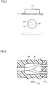
- Fig. 6 shows arrangement of the controller and the power supply over the outer circumference of the beam splitting member in Fig. 2 .
- Fig. 6 shows a cross section along line VI-VI in Fig. 2 .
- controller 36 and power supply 37 are arranged so that they are displaced from each other in the circumferential direction about the optical axis of objective lens 21. Controller 36 and power supply 37 are arranged opposite to each other with beam splitting member 24 (optical fiber 55) interposed therebetween, as seen in the optical axis direction of objective lens 21.
- CPU substrate 41 and power supply substrate 42 are arranged to be displaced from each other in the circumferential direction about the optical axis of objective lens 21.
- CPU substrate 41 and power supply substrate 42 are spaced from each other in the circumferential direction about the optical axis of objective lens 21.
- CPU substrate 41 and power supply substrate 42 are arranged opposite to each other with beam splitting member 24 (optical fiber 55) interposed therebetween, as seen in the optical axis direction of objective lens 21.
- CPU substrate 41 and power supply substrate 42 are arranged in parallel to each other.
- Controller 36 and power supply 37 are disposed at respective positions overlapping each other in the optical axis direction of objective lens 21. Controller 36 and power supply 37 may be arranged away from each other in the optical axis direction of objective lens 21. Preferably, the distance between controller 36 and beam splitting member 24 (optical fiber 55) is substantially equal to the distance between power supply 37 and beam splitting member 24 (optical fiber 55).
- Fig. 7 shows a comparative example of the arrangement of the electronic components and the substrates.
- an electronic component 112 and a substrate 111 on which electronic component 112 is mounted are disposed over the outer circumferential surface of optical fiber 55.
- Electronic component 112 and substrate 111 are disposed on only one side of optical fiber 55 about the optical axis of objective lens 21.
- operation of the colorimeter causes controller 36 mounted on CPU substrate 41 to generate heat and power supply 37 mounted on power supply substrate 42 to generate heat.
- optical fiber 55 is heated in the respective two directions in which controller 36 and power supply 37 are disposed. Accordingly, as indicated by two-dot chain lines 110 in Fig. 6 , the temperature distribution curves of optical fiber 55 are symmetrical with respect to the optical axis of objective lens 21. Thus, change of the degree of bending or posture of optical fiber 55 can be suppressed. Even when optical fiber 55 is deformed, the deformation can be prevented from being asymmetrical with respect to the optical axis of objective lens 21. As a result, the spectral sensitivity correction filter can exhibit desired spectral sensitivity characteristics, and deterioration of the measurement accuracy can be prevented.
- controller 36 and power supply 37 In the foregoing, only the positional relation between controller 36 and power supply 37 is described.
- the positional relation between controller 36 and data memory 32 mounted on CPU substrate 41 and power supply 37 and communication unit 38 mounted on power supply substrate 42 is similar to the positional relation between controller 36 and power supply 37.
- Fig. 8 is a cross-sectional view showing a specific configuration of the beam splitting member in Fig. 2 .
- beam splitting member 24 further includes a protective member 57.
- Protective member 57 is disposed to cover optical fiber 55 to protect optical fiber 55.
- Protective member 57 as a whole extends in a tubular shape (scabbard shape) around optical fiber 55.
- Optical fiber 55 is received in protective member 57.
- Protective member 57 is disposed to support the opposite ends of optical fiber 55.
- protective member 57 is formed of a combination of a tubular portion 57m and a lid portion 57n.
- Tubular portion 57m supports one end of optical fiber 55 and extends, in a tubular shape, from this one end toward the other end of optical fiber 55.
- Tubular member 57m is closed at the other end of optical fiber 55.
- Lid portion 57n is disposed to close the opening of tubular portion 57m. Lid portion 57n supports the other end of optical fiber 55.
- Optical fiber 55 is disposed so as not to be in contact with protective member 57, except for its part supported by protective member 57. Therefore, an air layer 58 is formed between optical fiber 55 and protective member 57. When heat is generated from controller 36 and power supply 37, air layer 58 can serve as a heat insulating layer to suppress temperature increase of optical fiber 55.
- Protective member 57 may be formed of a metal.
- the metal forming protective member 57 is preferably a metal having a high thermal conductivity. Aluminum, brass, or the like, for example, may be used for protective member 57. In this case, heat conduction through protective member 57 can be promoted to enhance the uniformity of thermal distribution in optical fiber 55.
- Protective member 57 may be formed of a heat insulator. Typical examples of the heat insulator are a variety of resin materials. In this case, heat transfer from controller 36 and power supply 37 to optical fiber 55 can be suppressed to thereby suppress temperature increase of optical fiber 55.
- Figs. 9 to 12 are cross-sectional views showing various modifications of the arrangement of the controller and the power supply in Fig. 6 .
- controller 36 CPU substrate 41
- power supply 37 power supply substrate 42
- CPU substrate 41 and power supply substrate 42 are arranged in respective postures extending at an angle of 90° therebetween.
- controller 36 (CPU substrate 41) and power supply 37 (power supply substrate 42) are displaced from each other at an angle therebetween smaller than 90° in the circumferential direction about optical axis of objective lens 21.
- CPU substrate 41 and power supply substrate 42 are disposed in respective postures extending at an angle therebetween larger than 90° and smaller than 180°.
- the angle at which controller 36 and power supply 37 are displaced from each other in the circumferential direction is not particularly limited.
- controller 36 CPU substrate 41
- power supply 37 power supply substrate 42
- controller 36, data memory 32 and power supply 37 are displaced from each other in the circumferential direction about the optical axis of objective lens 21. Controller 36, data memory 32, and power supply 37 are mounted on a single substrate 44. As illustrated in this modification, a plurality of electronic components displaced from each other in the circumferential direction may be mounted on the same substrate.
- Tristimulus photoelectric colorimeter 10 as an optical device for measurement in the present embodiment includes: objective lens 21 as an entrance unit to allow light from an object to be measured to enter, photoelectric converter 25 to convert received light into an electrical signal; beam splitting member 24 as an optical guide to guide the light entering through objective lens 21 to photoelectric converter 25; and controller 36 as a first electronic component and power supply 37 as a second electronic component that are arranged around an optical axis of beam splitting member 24 and displaced from each other in the circumferential direction.
- Tristimulus photoelectric colorimeter 10 includes: objective lens 21 as an entrance unit to allow light from an object to be measured to enter; beam splitting member 24 as an optical guide disposed on the optical axis of the light entering though objective lens 21 to guide the light entering through objective lens 21; photoelectric converter 25 receiving the light guided through beam splitting member 24 to convert the light into an electrical signal; and controller 36 as a first electronic component and power supply 37 as a second electronic component that are disposed over the outer circumference of beam splitting member 24 about the optical axis of the light entering through objective lens 21 and displaced from each other in the circumferential direction to process the electrical signal from photoelectric converter 25.
- tristimulus photoelectric colorimeter 10 in the present embodiment of the invention configured in this manner, deterioration of the measurement accuracy for photometry and colorimetry of the colorimeter due to heat generation from controller 36 and power supply 37 can be suppressed.
- the present embodiment is described in connection with tristimulus photoelectric colorimeter 10 capable of both photometry and colorimetry, the present invention is not limited to this and may be applied to an optical device capable of only one of photometry and colorimetry.
- the present invention is also applicable to a colorimeter based on spectrocolorimetry.
- An optical device for measurement includes: an entrance unit to allow light from an object to be measured to enter; a photoelectric converter to convert received light into an electrical signal; an optical guide to guide the light entering through the entrance unit to the photoelectric converter; and a first electronic component and a second electronic component disposed around an optical axis of the optical guide and displaced from each other in a circumferential direction.
- the first electronic component and the second electronic component as heat sources are displaced from each other in the circumferential direction, so that the influence of heat from these electronic components on the optical guide can be made more uniform around the optical axis of the optical guide. Accordingly, deterioration of the measurement accuracy of the optical device, due to heat generated from the electronic components, can be suppressed.
- the first electronic component and the second electronic component are disposed opposite to each other with respect to the optical guide as seen in a direction of an optical axis of the light entering through the entrance unit.
- influence of heat from the first and second electronic components on the optical guide can be made further uniform around the optical axis of the light entering through the entrance unit.
- the first electronic component is a controller to control measurement operation by the optical device for measurement.
- the second electronic component is a power supply to transform externally supplied electric power.
- the controller and the power supply generating a greater amount of heat are displaced from each other in the circumferential direction over the outer circumference of the optical guide, and therefore, the advantageous effect of suppressing deterioration of the measurement accuracy can be produced more effectively.
- the optical guide includes: an optical fiber to propagate light; and a protective member disposed to cover the optical fiber and protect the optical fiber.
- the optical fiber can be protected against externally applied vibration and/or impact.
- an air layer is formed between the optical fiber and the protective member.
- the protective member is formed of a heat insulator.
- heat conduction by the protective member can be promoted to further make uniform the influence of heat from the first and second electronic components on the optical fiber around the optical axis of the light entering through the entrance unit.
- the protective member is formed of a heat insulator.
- the optical device for measurement further includes a first substrate on which the first electronic component is mounted and a second substrate on which the second electronic component is mounted.
- influence of heat, on the optical guide, from the first and second electronic components mounted on the first and second substrates respectively can be made more uniform around the optical axis of the light entering through the entrance unit.
- the optical device for measurement further includes a plurality of substrates each extending in a plate shape along a direction of an optical axis of the light entering through the entrance unit.
- the optical guide has a first facing surface facing the entrance unit and a second facing surface facing the photoelectric converter, in the direction of the optical axis of the light entering through the entrance unit. All of the substrates are disposed between the first facing surface and the second facing surface in the direction of the optical axis of the light entering through the entrance unit.
- the optical device can be reduced in size in the direction of the optical axis of the light entering through the entrance unit.
- the present invention is applicable for example to tristimulus photoelectric colorimeters.
Landscapes
- Physics & Mathematics (AREA)
- Spectroscopy & Molecular Physics (AREA)
- General Physics & Mathematics (AREA)
- Electromagnetism (AREA)
- Spectrometry And Color Measurement (AREA)
Applications Claiming Priority (2)
| Application Number | Priority Date | Filing Date | Title |
|---|---|---|---|
| JP2015233288 | 2015-11-30 | ||
| PCT/JP2016/084597 WO2017094562A1 (fr) | 2015-11-30 | 2016-11-22 | Dispositif optique de mesure |
Publications (3)
| Publication Number | Publication Date |
|---|---|
| EP3385687A1 true EP3385687A1 (fr) | 2018-10-10 |
| EP3385687A4 EP3385687A4 (fr) | 2019-01-09 |
| EP3385687B1 EP3385687B1 (fr) | 2023-10-25 |
Family
ID=58797177
Family Applications (1)
| Application Number | Title | Priority Date | Filing Date |
|---|---|---|---|
| EP16870499.7A Active EP3385687B1 (fr) | 2015-11-30 | 2016-11-22 | Dispositif optique de mesure |
Country Status (5)
| Country | Link |
|---|---|
| EP (1) | EP3385687B1 (fr) |
| JP (1) | JP6750634B2 (fr) |
| KR (1) | KR102100573B1 (fr) |
| CN (1) | CN108291839B (fr) |
| WO (1) | WO2017094562A1 (fr) |
Family Cites Families (15)
| Publication number | Priority date | Publication date | Assignee | Title |
|---|---|---|---|---|
| IT1216681B (it) * | 1988-03-31 | 1990-03-08 | Maxmeyer Duco Mm D Spa | Spettrofometro portatile. |
| US6249348B1 (en) * | 1998-11-23 | 2001-06-19 | Lj Laboratories, L.L.C. | Integrated spectrometer assembly and methods |
| JP4333050B2 (ja) | 2001-04-17 | 2009-09-16 | コニカミノルタセンシング株式会社 | 測定用光学系及びこの光学系を備えた三刺激値型光電色彩計 |
| JP2003315566A (ja) * | 2002-02-22 | 2003-11-06 | Sumitomo Metal Mining Co Ltd | 光ファイバフィードスルー |
| CN100390512C (zh) * | 2003-11-27 | 2008-05-28 | 中国科学院半导体研究所 | 单光子探测装置的结构 |
| DE102004023156A1 (de) * | 2004-05-07 | 2005-12-15 | Siemens Ag | Sensor zur Bestimmung von Messgrößen, die zur Steuerung einer Klimaanlage und anderer ein Raumklima beeinflussenden Vorrichtungen geeignet sind |
| DE102007028606A1 (de) * | 2007-06-19 | 2008-12-24 | Behr-Hella Thermocontrol Gmbh | Sonnensensor mit Lichtwellenleiter |
| JP2010002255A (ja) * | 2008-06-19 | 2010-01-07 | Topcon Corp | 測定用光学系 |
| JP2010025558A (ja) * | 2008-07-15 | 2010-02-04 | Topcon Corp | 測定用光学系 |
| EP2570785B1 (fr) * | 2010-05-14 | 2019-05-15 | Konica Minolta Optics, Inc. | Système optique de mesure, et luminancemètre, luminancemètre couleur et colorimètre utilisant ce système optique |
| CN201772882U (zh) * | 2010-07-06 | 2011-03-23 | 北京自动化控制设备研究所 | 一种用于光纤陀螺仪的隔热装置 |
| KR101361175B1 (ko) * | 2012-06-14 | 2014-02-10 | (주)에이앤아이 | 컬리메이터 렌즈 및 집광렌즈를 구비한 색차계모듈 및 이를 이용한 색상계측기 |
| CN203101252U (zh) * | 2013-01-16 | 2013-07-31 | 中国石油天然气集团公司 | 一种用于贯穿光纤束的金属绝热瓶 |
| JP2015202316A (ja) * | 2014-04-16 | 2015-11-16 | 学校法人日本大学 | 光学的イメージング医療システム及びカメラ |
| JP2015204580A (ja) * | 2014-04-16 | 2015-11-16 | キヤノン株式会社 | 撮像装置 |
-
2016
- 2016-11-22 EP EP16870499.7A patent/EP3385687B1/fr active Active
- 2016-11-22 KR KR1020187014540A patent/KR102100573B1/ko active Active
- 2016-11-22 WO PCT/JP2016/084597 patent/WO2017094562A1/fr not_active Ceased
- 2016-11-22 CN CN201680069698.XA patent/CN108291839B/zh active Active
- 2016-11-22 JP JP2017553791A patent/JP6750634B2/ja active Active
Also Published As
| Publication number | Publication date |
|---|---|
| EP3385687B1 (fr) | 2023-10-25 |
| EP3385687A4 (fr) | 2019-01-09 |
| KR20180072794A (ko) | 2018-06-29 |
| CN108291839A (zh) | 2018-07-17 |
| JP6750634B2 (ja) | 2020-09-02 |
| WO2017094562A1 (fr) | 2017-06-08 |
| KR102100573B1 (ko) | 2020-04-13 |
| CN108291839B (zh) | 2021-07-13 |
| JPWO2017094562A1 (ja) | 2018-09-13 |
Similar Documents
| Publication | Publication Date | Title |
|---|---|---|
| US20120188646A1 (en) | Variable wavelength interference filter, optical module, and optical analysis device | |
| KR20250133449A (ko) | 광학 장치, 색채 휘도계 및 색채계 | |
| US6459485B1 (en) | Optical system | |
| CN106092394A (zh) | 基于光纤法珀传感器的高温应变测量系统及方法 | |
| JP7200936B2 (ja) | 測定用光学系、色彩輝度計および色彩計 | |
| KR20200118349A (ko) | 광학 방출 분석 캘리브레이션 장치 및 시스템 | |
| EP3385687B1 (fr) | Dispositif optique de mesure | |
| JP2010133833A (ja) | 測光装置 | |
| JP2017150935A (ja) | 光特性測定システムおよび測定用光学装置 | |
| JP5686230B1 (ja) | 照明装置及び反射特性測定装置 | |
| WO2015107656A1 (fr) | Appareil de mesure optique | |
| CN102435349B (zh) | 通信c波段半导体吸收型光纤温度敏感单元及传感系统 | |
| JP6692614B2 (ja) | 測定器 | |
| US20190063995A1 (en) | Color parameter measurement device and color parameter measurement method | |
| JP6682896B2 (ja) | 測光または測色のための装置 | |
| CN120051671A (zh) | 测定用光学装置 | |
| WO2026053720A1 (fr) | Dispositif photométrique/colorimétrique | |
| CN212459386U (zh) | 一种光学测量仪器 | |
| WO2026053726A1 (fr) | Dispositif photométrique/colorimétrique | |
| WO2016208462A1 (fr) | Dispositif de mesure et procédé de fabrication de dispositif de mesure | |
| JP2025186750A (ja) | 分光器及び光学装置 | |
| CN104374475B (zh) | 大视场超光谱成像差分吸收光谱仪装星测试装置 | |
| JP6331986B2 (ja) | 光学特性測定装置 | |
| JPS5939619Y2 (ja) | 光フアイバ−光学補正装置 | |
| KR101542468B1 (ko) | 반도체 웨이퍼 열특성 분석 장치 |
Legal Events
| Date | Code | Title | Description |
|---|---|---|---|
| STAA | Information on the status of an ep patent application or granted ep patent |
Free format text: STATUS: THE INTERNATIONAL PUBLICATION HAS BEEN MADE |
|
| PUAI | Public reference made under article 153(3) epc to a published international application that has entered the european phase |
Free format text: ORIGINAL CODE: 0009012 |
|
| STAA | Information on the status of an ep patent application or granted ep patent |
Free format text: STATUS: REQUEST FOR EXAMINATION WAS MADE |
|
| 17P | Request for examination filed |
Effective date: 20180607 |
|
| AK | Designated contracting states |
Kind code of ref document: A1 Designated state(s): AL AT BE BG CH CY CZ DE DK EE ES FI FR GB GR HR HU IE IS IT LI LT LU LV MC MK MT NL NO PL PT RO RS SE SI SK SM TR |
|
| AX | Request for extension of the european patent |
Extension state: BA ME |
|
| A4 | Supplementary search report drawn up and despatched |
Effective date: 20181207 |
|
| RIC1 | Information provided on ipc code assigned before grant |
Ipc: G01J 3/50 20060101AFI20181203BHEP Ipc: G01J 3/02 20060101ALI20181203BHEP Ipc: G01J 1/02 20060101ALI20181203BHEP |
|
| DAV | Request for validation of the european patent (deleted) | ||
| DAX | Request for extension of the european patent (deleted) | ||
| STAA | Information on the status of an ep patent application or granted ep patent |
Free format text: STATUS: EXAMINATION IS IN PROGRESS |
|
| 17Q | First examination report despatched |
Effective date: 20211005 |
|
| GRAP | Despatch of communication of intention to grant a patent |
Free format text: ORIGINAL CODE: EPIDOSNIGR1 |
|
| STAA | Information on the status of an ep patent application or granted ep patent |
Free format text: STATUS: GRANT OF PATENT IS INTENDED |
|
| P01 | Opt-out of the competence of the unified patent court (upc) registered |
Effective date: 20230510 |
|
| INTG | Intention to grant announced |
Effective date: 20230523 |
|
| GRAS | Grant fee paid |
Free format text: ORIGINAL CODE: EPIDOSNIGR3 |
|
| GRAA | (expected) grant |
Free format text: ORIGINAL CODE: 0009210 |
|
| STAA | Information on the status of an ep patent application or granted ep patent |
Free format text: STATUS: THE PATENT HAS BEEN GRANTED |
|
| AK | Designated contracting states |
Kind code of ref document: B1 Designated state(s): AL AT BE BG CH CY CZ DE DK EE ES FI FR GB GR HR HU IE IS IT LI LT LU LV MC MK MT NL NO PL PT RO RS SE SI SK SM TR |
|
| REG | Reference to a national code |
Ref country code: GB Ref legal event code: FG4D |
|
| REG | Reference to a national code |
Ref country code: CH Ref legal event code: EP |
|
| REG | Reference to a national code |
Ref country code: DE Ref legal event code: R096 Ref document number: 602016083738 Country of ref document: DE |
|
| REG | Reference to a national code |
Ref country code: IE Ref legal event code: FG4D |
|
| REG | Reference to a national code |
Ref country code: NL Ref legal event code: FP |
|
| REG | Reference to a national code |
Ref country code: LT Ref legal event code: MG9D |
|
| REG | Reference to a national code |
Ref country code: AT Ref legal event code: MK05 Ref document number: 1625108 Country of ref document: AT Kind code of ref document: T Effective date: 20231025 |
|
| PG25 | Lapsed in a contracting state [announced via postgrant information from national office to epo] |
Ref country code: GR Free format text: LAPSE BECAUSE OF FAILURE TO SUBMIT A TRANSLATION OF THE DESCRIPTION OR TO PAY THE FEE WITHIN THE PRESCRIBED TIME-LIMIT Effective date: 20240126 |
|
| PG25 | Lapsed in a contracting state [announced via postgrant information from national office to epo] |
Ref country code: IS Free format text: LAPSE BECAUSE OF FAILURE TO SUBMIT A TRANSLATION OF THE DESCRIPTION OR TO PAY THE FEE WITHIN THE PRESCRIBED TIME-LIMIT Effective date: 20240225 |
|
| PG25 | Lapsed in a contracting state [announced via postgrant information from national office to epo] |
Ref country code: LT Free format text: LAPSE BECAUSE OF FAILURE TO SUBMIT A TRANSLATION OF THE DESCRIPTION OR TO PAY THE FEE WITHIN THE PRESCRIBED TIME-LIMIT Effective date: 20231025 |
|
| PG25 | Lapsed in a contracting state [announced via postgrant information from national office to epo] |
Ref country code: AT Free format text: LAPSE BECAUSE OF FAILURE TO SUBMIT A TRANSLATION OF THE DESCRIPTION OR TO PAY THE FEE WITHIN THE PRESCRIBED TIME-LIMIT Effective date: 20231025 |
|
| PG25 | Lapsed in a contracting state [announced via postgrant information from national office to epo] |
Ref country code: ES Free format text: LAPSE BECAUSE OF FAILURE TO SUBMIT A TRANSLATION OF THE DESCRIPTION OR TO PAY THE FEE WITHIN THE PRESCRIBED TIME-LIMIT Effective date: 20231025 |
|
| PG25 | Lapsed in a contracting state [announced via postgrant information from national office to epo] |
Ref country code: LT Free format text: LAPSE BECAUSE OF FAILURE TO SUBMIT A TRANSLATION OF THE DESCRIPTION OR TO PAY THE FEE WITHIN THE PRESCRIBED TIME-LIMIT Effective date: 20231025 Ref country code: IS Free format text: LAPSE BECAUSE OF FAILURE TO SUBMIT A TRANSLATION OF THE DESCRIPTION OR TO PAY THE FEE WITHIN THE PRESCRIBED TIME-LIMIT Effective date: 20240225 Ref country code: GR Free format text: LAPSE BECAUSE OF FAILURE TO SUBMIT A TRANSLATION OF THE DESCRIPTION OR TO PAY THE FEE WITHIN THE PRESCRIBED TIME-LIMIT Effective date: 20240126 Ref country code: ES Free format text: LAPSE BECAUSE OF FAILURE TO SUBMIT A TRANSLATION OF THE DESCRIPTION OR TO PAY THE FEE WITHIN THE PRESCRIBED TIME-LIMIT Effective date: 20231025 Ref country code: BG Free format text: LAPSE BECAUSE OF FAILURE TO SUBMIT A TRANSLATION OF THE DESCRIPTION OR TO PAY THE FEE WITHIN THE PRESCRIBED TIME-LIMIT Effective date: 20240125 Ref country code: AT Free format text: LAPSE BECAUSE OF FAILURE TO SUBMIT A TRANSLATION OF THE DESCRIPTION OR TO PAY THE FEE WITHIN THE PRESCRIBED TIME-LIMIT Effective date: 20231025 Ref country code: PT Free format text: LAPSE BECAUSE OF FAILURE TO SUBMIT A TRANSLATION OF THE DESCRIPTION OR TO PAY THE FEE WITHIN THE PRESCRIBED TIME-LIMIT Effective date: 20240226 |
|
| PG25 | Lapsed in a contracting state [announced via postgrant information from national office to epo] |
Ref country code: SE Free format text: LAPSE BECAUSE OF FAILURE TO SUBMIT A TRANSLATION OF THE DESCRIPTION OR TO PAY THE FEE WITHIN THE PRESCRIBED TIME-LIMIT Effective date: 20231025 Ref country code: RS Free format text: LAPSE BECAUSE OF FAILURE TO SUBMIT A TRANSLATION OF THE DESCRIPTION OR TO PAY THE FEE WITHIN THE PRESCRIBED TIME-LIMIT Effective date: 20231025 Ref country code: PL Free format text: LAPSE BECAUSE OF FAILURE TO SUBMIT A TRANSLATION OF THE DESCRIPTION OR TO PAY THE FEE WITHIN THE PRESCRIBED TIME-LIMIT Effective date: 20231025 Ref country code: NO Free format text: LAPSE BECAUSE OF FAILURE TO SUBMIT A TRANSLATION OF THE DESCRIPTION OR TO PAY THE FEE WITHIN THE PRESCRIBED TIME-LIMIT Effective date: 20240125 Ref country code: LV Free format text: LAPSE BECAUSE OF FAILURE TO SUBMIT A TRANSLATION OF THE DESCRIPTION OR TO PAY THE FEE WITHIN THE PRESCRIBED TIME-LIMIT Effective date: 20231025 Ref country code: HR Free format text: LAPSE BECAUSE OF FAILURE TO SUBMIT A TRANSLATION OF THE DESCRIPTION OR TO PAY THE FEE WITHIN THE PRESCRIBED TIME-LIMIT Effective date: 20231025 |
|
| REG | Reference to a national code |
Ref country code: CH Ref legal event code: PL |
|
| PG25 | Lapsed in a contracting state [announced via postgrant information from national office to epo] |
Ref country code: DK Free format text: LAPSE BECAUSE OF FAILURE TO SUBMIT A TRANSLATION OF THE DESCRIPTION OR TO PAY THE FEE WITHIN THE PRESCRIBED TIME-LIMIT Effective date: 20231025 |
|
| PG25 | Lapsed in a contracting state [announced via postgrant information from national office to epo] |
Ref country code: LU Free format text: LAPSE BECAUSE OF NON-PAYMENT OF DUE FEES Effective date: 20231122 |
|
| PG25 | Lapsed in a contracting state [announced via postgrant information from national office to epo] |
Ref country code: CH Free format text: LAPSE BECAUSE OF NON-PAYMENT OF DUE FEES Effective date: 20231130 |
|
| PG25 | Lapsed in a contracting state [announced via postgrant information from national office to epo] |
Ref country code: CZ Free format text: LAPSE BECAUSE OF FAILURE TO SUBMIT A TRANSLATION OF THE DESCRIPTION OR TO PAY THE FEE WITHIN THE PRESCRIBED TIME-LIMIT Effective date: 20231025 |
|
| REG | Reference to a national code |
Ref country code: DE Ref legal event code: R097 Ref document number: 602016083738 Country of ref document: DE |
|
| PG25 | Lapsed in a contracting state [announced via postgrant information from national office to epo] |
Ref country code: SK Free format text: LAPSE BECAUSE OF FAILURE TO SUBMIT A TRANSLATION OF THE DESCRIPTION OR TO PAY THE FEE WITHIN THE PRESCRIBED TIME-LIMIT Effective date: 20231025 |
|
| PG25 | Lapsed in a contracting state [announced via postgrant information from national office to epo] |
Ref country code: SM Free format text: LAPSE BECAUSE OF FAILURE TO SUBMIT A TRANSLATION OF THE DESCRIPTION OR TO PAY THE FEE WITHIN THE PRESCRIBED TIME-LIMIT Effective date: 20231025 Ref country code: SK Free format text: LAPSE BECAUSE OF FAILURE TO SUBMIT A TRANSLATION OF THE DESCRIPTION OR TO PAY THE FEE WITHIN THE PRESCRIBED TIME-LIMIT Effective date: 20231025 Ref country code: RO Free format text: LAPSE BECAUSE OF FAILURE TO SUBMIT A TRANSLATION OF THE DESCRIPTION OR TO PAY THE FEE WITHIN THE PRESCRIBED TIME-LIMIT Effective date: 20231025 Ref country code: LU Free format text: LAPSE BECAUSE OF NON-PAYMENT OF DUE FEES Effective date: 20231122 Ref country code: IT Free format text: LAPSE BECAUSE OF FAILURE TO SUBMIT A TRANSLATION OF THE DESCRIPTION OR TO PAY THE FEE WITHIN THE PRESCRIBED TIME-LIMIT Effective date: 20231025 Ref country code: EE Free format text: LAPSE BECAUSE OF FAILURE TO SUBMIT A TRANSLATION OF THE DESCRIPTION OR TO PAY THE FEE WITHIN THE PRESCRIBED TIME-LIMIT Effective date: 20231025 Ref country code: DK Free format text: LAPSE BECAUSE OF FAILURE TO SUBMIT A TRANSLATION OF THE DESCRIPTION OR TO PAY THE FEE WITHIN THE PRESCRIBED TIME-LIMIT Effective date: 20231025 Ref country code: CZ Free format text: LAPSE BECAUSE OF FAILURE TO SUBMIT A TRANSLATION OF THE DESCRIPTION OR TO PAY THE FEE WITHIN THE PRESCRIBED TIME-LIMIT Effective date: 20231025 Ref country code: CH Free format text: LAPSE BECAUSE OF NON-PAYMENT OF DUE FEES Effective date: 20231130 |
|
| REG | Reference to a national code |
Ref country code: BE Ref legal event code: MM Effective date: 20231130 |
|
| PG25 | Lapsed in a contracting state [announced via postgrant information from national office to epo] |
Ref country code: MC Free format text: LAPSE BECAUSE OF FAILURE TO SUBMIT A TRANSLATION OF THE DESCRIPTION OR TO PAY THE FEE WITHIN THE PRESCRIBED TIME-LIMIT Effective date: 20231025 |
|
| PG25 | Lapsed in a contracting state [announced via postgrant information from national office to epo] |
Ref country code: MC Free format text: LAPSE BECAUSE OF FAILURE TO SUBMIT A TRANSLATION OF THE DESCRIPTION OR TO PAY THE FEE WITHIN THE PRESCRIBED TIME-LIMIT Effective date: 20231025 |
|
| PLBE | No opposition filed within time limit |
Free format text: ORIGINAL CODE: 0009261 |
|
| STAA | Information on the status of an ep patent application or granted ep patent |
Free format text: STATUS: NO OPPOSITION FILED WITHIN TIME LIMIT |
|
| REG | Reference to a national code |
Ref country code: IE Ref legal event code: MM4A |
|
| GBPC | Gb: european patent ceased through non-payment of renewal fee |
Effective date: 20240125 |
|
| 26N | No opposition filed |
Effective date: 20240726 |
|
| PG25 | Lapsed in a contracting state [announced via postgrant information from national office to epo] |
Ref country code: IE Free format text: LAPSE BECAUSE OF NON-PAYMENT OF DUE FEES Effective date: 20231122 |
|
| PG25 | Lapsed in a contracting state [announced via postgrant information from national office to epo] |
Ref country code: GB Free format text: LAPSE BECAUSE OF NON-PAYMENT OF DUE FEES Effective date: 20240125 |
|
| PG25 | Lapsed in a contracting state [announced via postgrant information from national office to epo] |
Ref country code: BE Free format text: LAPSE BECAUSE OF NON-PAYMENT OF DUE FEES Effective date: 20231130 |
|
| PG25 | Lapsed in a contracting state [announced via postgrant information from national office to epo] |
Ref country code: FR Free format text: LAPSE BECAUSE OF NON-PAYMENT OF DUE FEES Effective date: 20231225 |
|
| PG25 | Lapsed in a contracting state [announced via postgrant information from national office to epo] |
Ref country code: SI Free format text: LAPSE BECAUSE OF FAILURE TO SUBMIT A TRANSLATION OF THE DESCRIPTION OR TO PAY THE FEE WITHIN THE PRESCRIBED TIME-LIMIT Effective date: 20231025 |
|
| PG25 | Lapsed in a contracting state [announced via postgrant information from national office to epo] |
Ref country code: SI Free format text: LAPSE BECAUSE OF FAILURE TO SUBMIT A TRANSLATION OF THE DESCRIPTION OR TO PAY THE FEE WITHIN THE PRESCRIBED TIME-LIMIT Effective date: 20231025 Ref country code: IE Free format text: LAPSE BECAUSE OF NON-PAYMENT OF DUE FEES Effective date: 20231122 Ref country code: GB Free format text: LAPSE BECAUSE OF NON-PAYMENT OF DUE FEES Effective date: 20240125 Ref country code: FR Free format text: LAPSE BECAUSE OF NON-PAYMENT OF DUE FEES Effective date: 20231225 Ref country code: BE Free format text: LAPSE BECAUSE OF NON-PAYMENT OF DUE FEES Effective date: 20231130 |
|
| PG25 | Lapsed in a contracting state [announced via postgrant information from national office to epo] |
Ref country code: FI Free format text: LAPSE BECAUSE OF FAILURE TO SUBMIT A TRANSLATION OF THE DESCRIPTION OR TO PAY THE FEE WITHIN THE PRESCRIBED TIME-LIMIT Effective date: 20231025 |
|
| PG25 | Lapsed in a contracting state [announced via postgrant information from national office to epo] |
Ref country code: CY Free format text: LAPSE BECAUSE OF FAILURE TO SUBMIT A TRANSLATION OF THE DESCRIPTION OR TO PAY THE FEE WITHIN THE PRESCRIBED TIME-LIMIT; INVALID AB INITIO Effective date: 20161122 |
|
| PG25 | Lapsed in a contracting state [announced via postgrant information from national office to epo] |
Ref country code: HU Free format text: LAPSE BECAUSE OF FAILURE TO SUBMIT A TRANSLATION OF THE DESCRIPTION OR TO PAY THE FEE WITHIN THE PRESCRIBED TIME-LIMIT; INVALID AB INITIO Effective date: 20161122 |
|
| PGFP | Annual fee paid to national office [announced via postgrant information from national office to epo] |
Ref country code: NL Payment date: 20251003 Year of fee payment: 10 |
|
| PG25 | Lapsed in a contracting state [announced via postgrant information from national office to epo] |
Ref country code: TR Free format text: LAPSE BECAUSE OF FAILURE TO SUBMIT A TRANSLATION OF THE DESCRIPTION OR TO PAY THE FEE WITHIN THE PRESCRIBED TIME-LIMIT Effective date: 20231025 |
|
| PGFP | Annual fee paid to national office [announced via postgrant information from national office to epo] |
Ref country code: DE Payment date: 20250930 Year of fee payment: 10 |