EP3385784A1 - Optoelektronische vorrichtung zur erzeugung eines frequenzkamms - Google Patents
Optoelektronische vorrichtung zur erzeugung eines frequenzkamms Download PDFInfo
- Publication number
- EP3385784A1 EP3385784A1 EP18161911.5A EP18161911A EP3385784A1 EP 3385784 A1 EP3385784 A1 EP 3385784A1 EP 18161911 A EP18161911 A EP 18161911A EP 3385784 A1 EP3385784 A1 EP 3385784A1
- Authority
- EP
- European Patent Office
- Prior art keywords
- resonant ring
- optical
- value
- ring
- resonant
- Prior art date
- Legal status (The legal status is an assumption and is not a legal conclusion. Google has not performed a legal analysis and makes no representation as to the accuracy of the status listed.)
- Granted
Links
Images


Classifications
-
- G—PHYSICS
- G02—OPTICS
- G02F—OPTICAL DEVICES OR ARRANGEMENTS FOR THE CONTROL OF LIGHT BY MODIFICATION OF THE OPTICAL PROPERTIES OF THE MEDIA OF THE ELEMENTS INVOLVED THEREIN; NON-LINEAR OPTICS; FREQUENCY-CHANGING OF LIGHT; OPTICAL LOGIC ELEMENTS; OPTICAL ANALOGUE/DIGITAL CONVERTERS
- G02F1/00—Devices or arrangements for the control of the intensity, colour, phase, polarisation or direction of light arriving from an independent light source, e.g. switching, gating or modulating; Non-linear optics
- G02F1/35—Non-linear optics
- G02F1/39—Non-linear optics for parametric generation or amplification of light, infrared or ultraviolet waves
- G02F1/395—Non-linear optics for parametric generation or amplification of light, infrared or ultraviolet waves in optical waveguides
-
- G—PHYSICS
- G02—OPTICS
- G02F—OPTICAL DEVICES OR ARRANGEMENTS FOR THE CONTROL OF LIGHT BY MODIFICATION OF THE OPTICAL PROPERTIES OF THE MEDIA OF THE ELEMENTS INVOLVED THEREIN; NON-LINEAR OPTICS; FREQUENCY-CHANGING OF LIGHT; OPTICAL LOGIC ELEMENTS; OPTICAL ANALOGUE/DIGITAL CONVERTERS
- G02F1/00—Devices or arrangements for the control of the intensity, colour, phase, polarisation or direction of light arriving from an independent light source, e.g. switching, gating or modulating; Non-linear optics
- G02F1/35—Non-linear optics
- G02F1/353—Frequency conversion, i.e. wherein a light beam is generated with frequency components different from those of the incident light beams
- G02F1/3536—Four-wave interaction
-
- G—PHYSICS
- G02—OPTICS
- G02F—OPTICAL DEVICES OR ARRANGEMENTS FOR THE CONTROL OF LIGHT BY MODIFICATION OF THE OPTICAL PROPERTIES OF THE MEDIA OF THE ELEMENTS INVOLVED THEREIN; NON-LINEAR OPTICS; FREQUENCY-CHANGING OF LIGHT; OPTICAL LOGIC ELEMENTS; OPTICAL ANALOGUE/DIGITAL CONVERTERS
- G02F1/00—Devices or arrangements for the control of the intensity, colour, phase, polarisation or direction of light arriving from an independent light source, e.g. switching, gating or modulating; Non-linear optics
- G02F1/35—Non-linear optics
- G02F1/365—Non-linear optics in an optical waveguide structure
-
- G—PHYSICS
- G02—OPTICS
- G02F—OPTICAL DEVICES OR ARRANGEMENTS FOR THE CONTROL OF LIGHT BY MODIFICATION OF THE OPTICAL PROPERTIES OF THE MEDIA OF THE ELEMENTS INVOLVED THEREIN; NON-LINEAR OPTICS; FREQUENCY-CHANGING OF LIGHT; OPTICAL LOGIC ELEMENTS; OPTICAL ANALOGUE/DIGITAL CONVERTERS
- G02F1/00—Devices or arrangements for the control of the intensity, colour, phase, polarisation or direction of light arriving from an independent light source, e.g. switching, gating or modulating; Non-linear optics
- G02F1/35—Non-linear optics
- G02F1/39—Non-linear optics for parametric generation or amplification of light, infrared or ultraviolet waves
- G02F1/392—Parametric amplification
-
- G—PHYSICS
- G02—OPTICS
- G02F—OPTICAL DEVICES OR ARRANGEMENTS FOR THE CONTROL OF LIGHT BY MODIFICATION OF THE OPTICAL PROPERTIES OF THE MEDIA OF THE ELEMENTS INVOLVED THEREIN; NON-LINEAR OPTICS; FREQUENCY-CHANGING OF LIGHT; OPTICAL LOGIC ELEMENTS; OPTICAL ANALOGUE/DIGITAL CONVERTERS
- G02F2201/00—Constructional arrangements not provided for in groups G02F1/00 - G02F7/00
- G02F2201/04—Constructional arrangements not provided for in groups G02F1/00 - G02F7/00 monomode
-
- G—PHYSICS
- G02—OPTICS
- G02F—OPTICAL DEVICES OR ARRANGEMENTS FOR THE CONTROL OF LIGHT BY MODIFICATION OF THE OPTICAL PROPERTIES OF THE MEDIA OF THE ELEMENTS INVOLVED THEREIN; NON-LINEAR OPTICS; FREQUENCY-CHANGING OF LIGHT; OPTICAL LOGIC ELEMENTS; OPTICAL ANALOGUE/DIGITAL CONVERTERS
- G02F2201/00—Constructional arrangements not provided for in groups G02F1/00 - G02F7/00
- G02F2201/58—Arrangements comprising a monitoring photodetector
-
- G—PHYSICS
- G02—OPTICS
- G02F—OPTICAL DEVICES OR ARRANGEMENTS FOR THE CONTROL OF LIGHT BY MODIFICATION OF THE OPTICAL PROPERTIES OF THE MEDIA OF THE ELEMENTS INVOLVED THEREIN; NON-LINEAR OPTICS; FREQUENCY-CHANGING OF LIGHT; OPTICAL LOGIC ELEMENTS; OPTICAL ANALOGUE/DIGITAL CONVERTERS
- G02F2202/00—Materials and properties
- G02F2202/10—Materials and properties semiconductor
- G02F2202/101—Ga×As and alloy
-
- G—PHYSICS
- G02—OPTICS
- G02F—OPTICAL DEVICES OR ARRANGEMENTS FOR THE CONTROL OF LIGHT BY MODIFICATION OF THE OPTICAL PROPERTIES OF THE MEDIA OF THE ELEMENTS INVOLVED THEREIN; NON-LINEAR OPTICS; FREQUENCY-CHANGING OF LIGHT; OPTICAL LOGIC ELEMENTS; OPTICAL ANALOGUE/DIGITAL CONVERTERS
- G02F2202/00—Materials and properties
- G02F2202/10—Materials and properties semiconductor
- G02F2202/102—In×P and alloy
-
- G—PHYSICS
- G02—OPTICS
- G02F—OPTICAL DEVICES OR ARRANGEMENTS FOR THE CONTROL OF LIGHT BY MODIFICATION OF THE OPTICAL PROPERTIES OF THE MEDIA OF THE ELEMENTS INVOLVED THEREIN; NON-LINEAR OPTICS; FREQUENCY-CHANGING OF LIGHT; OPTICAL LOGIC ELEMENTS; OPTICAL ANALOGUE/DIGITAL CONVERTERS
- G02F2203/00—Function characteristic
- G02F2203/15—Function characteristic involving resonance effects, e.g. resonantly enhanced interaction
-
- G—PHYSICS
- G02—OPTICS
- G02F—OPTICAL DEVICES OR ARRANGEMENTS FOR THE CONTROL OF LIGHT BY MODIFICATION OF THE OPTICAL PROPERTIES OF THE MEDIA OF THE ELEMENTS INVOLVED THEREIN; NON-LINEAR OPTICS; FREQUENCY-CHANGING OF LIGHT; OPTICAL LOGIC ELEMENTS; OPTICAL ANALOGUE/DIGITAL CONVERTERS
- G02F2203/00—Function characteristic
- G02F2203/17—Function characteristic involving soliton waves
-
- G—PHYSICS
- G02—OPTICS
- G02F—OPTICAL DEVICES OR ARRANGEMENTS FOR THE CONTROL OF LIGHT BY MODIFICATION OF THE OPTICAL PROPERTIES OF THE MEDIA OF THE ELEMENTS INVOLVED THEREIN; NON-LINEAR OPTICS; FREQUENCY-CHANGING OF LIGHT; OPTICAL LOGIC ELEMENTS; OPTICAL ANALOGUE/DIGITAL CONVERTERS
- G02F2203/00—Function characteristic
- G02F2203/56—Frequency comb synthesizer
Definitions
- the field of the invention is that of optoelectronic devices for generating a quasi-coherent or coherent frequency comb by the formation of Kerr-type dissipative time solitons.
- a frequency comb is a representation of an optical signal in the frequency domain whose spectrum is composed of a discrete sum of frequencies. The amplitude can be weighted by a spectral envelope centered around the frequency w p of a pump signal.
- Such optoelectronic devices find their application particularly in the field of optical telecommunication, for example coherent data transmission networks, signal generation, fast spectroscopy or even time reference systems.
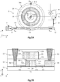
- the Figure 1A illustrates an example of such an optoelectronic device 1, described in the publication of Levy et al. titled CMOS-compatible multiple-wavelength oscillator for on-chip optical interconnects, Nature Photon. 4, 37-40 (2010) ), this optoelectronic device 1 being produced by CMOS microelectronics methods.
- It comprises a laser source 2 and an optical micro-resonator 3 ring.
- the laser source 2 is adapted to emit an optical signal S in said pump, continuous and monochromatic wavelength ⁇ p .
- the micro-resonator 3 comprises a coupling waveguide 10 having an input coupled to the laser source 2 and an output which provides an optical signal S out whose spectrum forms the generated frequency comb.
- It furthermore comprises an optical cavity formed of a ring waveguide 20, called a resonant ring, made of a material with nonlinear optical properties of the third order, in this case silicon nitride SiN.
- the optical micro-resonator 3 forms an optical parametric oscillator.
- the pump signal S in whose spectrum is represented on the Figure 1B , is resonantly coupled to a fundamental mode of the resonant ring 20 by evanescent wave.
- the material of the resonant ring 20 is optically non-linear of order three, that is to say that it possesses an electrical susceptibility of order three, a so-called four-wave cascade mixing phenomenon appears which generates, from the fundamental mode supported by the resonant ring 20, a frequency comb, an example of which is shown on FIG. figure 1 C .
- the non-linear optical effects of the material of the resonant ring cause an offset of the resonance wavelength ⁇ res towards the long wavelengths.
- the frequency sweep of the resonance shows that the latter has a shape no longer lorentzian but of triangular type, an example of which is shown in FIG. figure 1D .
- Herr 2014 shows that it is possible to form dissipative time solitons, which render the frequency comb generated quasi-coherent or coherent, performing a resonance scan by the pump frequency.
- the pump laser changes from a spectral chord to the optical cavity in the blue ( blue-detuning , in English) for which the pump frequency w p is greater than the effective resonance frequency w res , a spectral chord in the red ( red-detuning , in English) for which the pump frequency w p is lower than the effective resonance frequency w res , which then causes the formation of temporal solitons.
- the presence of solitons can be demonstrated in particular from the value Tr of the optical transmission signal which has, in the red-detuning regime , discrete transitions as the pump frequency w p decreases, these transitions reflecting the decrease the number of solitons propagating in the optical cavity.
- the frequency comb in the solitonic regime also has a greatly reduced noise, and its spectral envelope becomes sinh 2 when the comb is fully coherent (a single soliton in the optical cavity).
- the optoelectronic device for generating a quasi-coherent or coherent frequency comb described by Herr 2014 nevertheless has the disadvantage of having to achieve a particularly fine spectral tuning of the pump signal to the resonant mode. obtain the Rs solitonic regime, which requires the use of a laser source expensive, cumbersome and therefore difficult to integrate.
- the object of the invention is to remedy at least in part the drawbacks of the prior art, and more particularly to propose an optoelectronic device for generating a frequency comb allowing a simplified spectral agreement between the pump signal and a resonant mode. for the purpose of forming dissipative temporal solitons.
- Longitudinal optical coupling of the second waveguide with the resonant ring means that the optical coupling is made along the longitudinal axis of the second waveguide.
- semiconductor junction which extends parallel to the resonant ring is meant that the junction extends along a longitudinal axis, which is locally parallel to that of the resonant ring.
- the resonant ring and the junction guide are superimposed on each other. They may be coaxial, and preferably have a longitudinal shape substantially identical to each other.
- the control unit may be adapted to detect an optical signal at the output, to determine a value of a parameter representative of a spectral agreement between the pump signal and an optical mode of the ring resonating at the value of the applied voltage, and to induce a modification of the value of said applied voltage until the value of said parameter reaches a reference value representative of the presence of at least one dissipative time soliton in the resonant ring.
- the junction guide material may be silicon.
- the material of the resonant ring may be a III-V semiconductor compound, or an IV element or a compound IV, or even an IV-V compound.
- the material of the resonant ring may be selected from AlGaAs, GaAs, GaAsP, InGaP, InGaAsP, InGaAs.
- the resonant ring may be single-mode at the resonant wavelength.
- the difference between the refractive indices of the resonant ring and the junction guide may be less than or equal to 0.5.
- a mean distance separating the resonant ring and the junction guide, along an axis orthogonal to the plane along which the resonant ring extends, may be between 75 nm and 200 nm.
- An average width of the junction guide may be smaller than that of the resonant ring.
- the average width of the junction guide may be between 200 nm and 500 nm and that of the resonant ring may be between 400 nm and 800 nm.
- the materials of the resonant ring and the junction guide may be surrounded by a silicon oxide sheath.
- the pump wavelength may be less than the resonance wavelength.
- step d) changing the value of the bias voltage from the initial value may cause the resonant wavelength to decrease until it is less than the length of the resonance. pump wave.
- the value of an optical transmission of the optical micro-resonator can be determined, the reference value being a minimum value of the optical transmission when the value of the bias voltage increases.
- the invention relates to an optoelectronic device for generating a quasi-coherent or coherent frequency comb. It comprises an optical micro-resonator which forms an optical parametric oscillator, in which a frequency comb is generated by a cascading four-wave nonlinear mixing phenomenon associated with the formation of Kerr dissipative time solitons. .
- the frequency comb is said to be quasi-coherent when the frequency lines are partially in phase relation with each other, reflecting the presence of several time solitons. It is said to be coherent, or fully coherent, when all the frequency lines are in mutual phase relationship, which is the case when a single temporal soliton is present in the optical cavity.
- the operating regime of the frequency comb generator is called solitonic Rs when one or more time solitons are present.
- An optical parametric oscillator is a coherent light source that relies on parametric amplification in an optical resonator.
- the optical resonator here comprises an optical cavity made of a non-linear medium of the third order, that is to say comprising an electrical susceptibility ⁇ (3) of order three, allowing the mixture to four cascaded waves to take place, thus generating a frequency comb.
- the four-wave cascaded mixture is a third-order nonlinear phenomenon in which two photons of pump frequency w p are converted without loss of energy into a photon called a frequency signal w s and a so-called complementary photon ( idler , in english) of frequency w c . It is said cascaded insofar as the generated photons are also at the origin of the generation of other signal photons and complementary by mixing four waves.
- the optical Kerr effect is a third-order non-linear phenomenon that expresses the dependence of the refractive index of a medium on the intensity of the optical signal passing through it.
- the optical cavity of the micro-resonator is made of an optical Kerr effect material whose refractive index and opto-geometric dimensions are chosen to present an optical Kerr effect.
- the refractive index can be high, for example close to that of silicon, so that the ring waveguide has transverse dimensions such that it is then monomode.
- the dispersion is said to be abnormal when the dispersion parameter D is positive.
- This parameter D expressed in ps / (nm.km), is defined as the product of a size ⁇ 2 and of - 2 ⁇ c / ⁇ res 2 where ⁇ res is the wavelength of the fundamental mode supported by the resonant ring to which the pump signal is tuned, which is less than the pump wavelength ⁇ p when the solitonic regime is reached.
- the magnitude ⁇ 2 also called Group Velocity Dispersion (GVD) corresponds to the fact that the group speed of the optical signal is dependent on the wavelength of the signal.
- each waveguide has a lower face and an opposite upper face, and rests on a support at the lower face, and has lateral flanks extending from the upper face to the upper face. on the underside. It has transverse dimensions of height and width.
- height is meant the mean distance of the waveguide, and more specifically of the so-called core material, along the axis Z orthogonal to the plane of the support, between the lower and upper faces.
- width is meant the mean distance between the lateral flanks of the waveguide, and more specifically the core material, in a plane parallel to the plane of the support.
- the height and the width are preferably substantially constant along the longitudinal extent of the waveguide.
- the Figure 2A is a top view, schematic and partial, of an optoelectronic device 1 of frequency comb generation according to one embodiment, adapted to provide a quasi-coherent or coherent comb.
- This optoelectronic device 1 comprises a laser source 2 adapted to emit a continuous monochromatic optical signal, an optical ring micro-resonator 3, and a spectral tuning device 4 adapted to achieve the spectral tuning of the resonant mode with the pump signal. by modifying the effective index of the resonant mode supported by the micro-resonator 3, so as to obtain the solitonic regime Rs.
- Figure 2B is a cross-sectional view of the resonant ring 20 and the junction guide 30 along a plane AA illustrated in FIG. Figure 2A .
- a three-dimensional orthogonal coordinate system (X, Y, Z) is defined in which the X and Y axes form a plane parallel to the planes along which the waveguides of the optoelectronic device rest, and where the Z axis is oriented according to the thickness dimension of the waveguides.
- the laser source 2 is adapted to emit an optical signal S in said pump.
- This optical signal is continuous and monochromatic, wavelength ⁇ p .
- the pump wavelength ⁇ p is then substantially constant over time. It is chosen to be able to resonantly excite a fundamental mode supported by the resonant ring 20 of the optical micro-resonator 3. For example, it may be equal to about 1.55 ⁇ m in the case of an application called telecom, or even be equal to 1.31 .mu.m for an application called datacom, or even be a wavelength of the visible or infrared, particularly the infrared medium.
- the pump wavelength ⁇ p is designed to excite a fundamental mode of the resonant ring 20 without the solitonic regime being initially reached. Indeed, insofar as the resonant ring 20 is in a non-linear three-order effect material, the effective resonance wavelength ⁇ res is greater than the linear resonance wavelength (due to the non-Lorentzian triangular shape of the resonance spectrum), the pump wavelength ⁇ p is initially lower than the effective resonance wavelength ⁇ res , thus resulting in a spectral agreement in the blue ( blue-detuning ) as shown on the figure 3B .
- the transition to spectral tuning in red ( red-detuning ) to address the solitonic regime Rs is performed by the spectral tuning device 4 described below.
- the power of the pump signal is chosen to be greater than the optical losses present in the optical micro-resonator 3, so that the parametric gain is greater than the optical losses and the amplification of the optical signal in the microphone optical resonator 3 can generate a frequency comb by mixing four waves in cascade.
- the laser source 2 can be carried on the sheath layer 52 surrounding the coupling guide 10 and the resonant ring 20, or even be integrated inside this layer 52.
- the ring optical micro-resonator 3 comprises a coupling waveguide 10 and a first ring waveguide 20, called a resonant ring.
- the coupling waveguide 10 comprises an input 11 and an output 12, which also form the input and the output of the optical micro-resonator 3.
- the input 11 is optically coupled to the laser source 2 to receive the signal of pump S in emitted by it, and the output 12 is adapted to provide the generated frequency comb. It comprises a coupling zone 13 for optical coupling to the resonant ring 20 by evanescent wave.
- the coupling waveguide 10 is made of a so-called high refractive index core material. More specifically, it comprises a core formed of a high refractive index material surrounded by a sheath 52 formed of a material of low refractive index.
- the guide 10 rests on a surface of a support layer 50 whose material participates in forming the sheath.
- the core material of the guide 10 is preferably identical to that of the resonant ring 20, and may be chosen from III-V semiconductor compounds comprising at least one element of column III and at least one element of column V of the periodic table, or among semiconductor elements or compounds IV or IV-V having at least one element of column IV.
- compounds III-V can be, among others, AlGaAs, GaAs, InGaAs, InGaAsP, InGaP.
- the elements or compounds IV or IV-V may be Si or SiN such as Si 3 N 4 .
- the cladding material may be, inter alia, silicon oxide SiO, for example SiO 2 .
- the waveguide 10 extends longitudinally between the inlet 11 and the outlet 12, with a shape that can be arbitrary.
- the transverse dimensions of the waveguide 10 may range from a few hundred nanometers to several micrometers.
- the waveguide 10 may be single mode or multimode. In this example, it is preferably monomode and supports a mode of type TE (transverse electric).
- the first ring waveguide 20, called the resonant ring forms the optical cavity of the micro-resonator 3.
- the resonant ring 20 comprises a third-order nonlinear material for generating optical waves. wavelengths different from the resonance wavelength by cascade four-wave mixing.
- the resonant ring 20 is sized and has a refractive index so that the chromatic dispersion is abnormal for the resonant optical mode.
- it is possible to form one or more Kerr dissipative time solitons making it possible to render the frequency comb generated by the cascaded four-wave mixture quasi-coherent or coherent.
- the resonant ring 20 is a ring-shaped waveguide. It comprises an optical coupling zone for being coupled by evanescent wave waveguide 10. It can extend in the form of a circle, an oval or other. In this example, it has a circle shape whose radius r is defined from a longitudinal line running through the transverse barycentres of the resonant ring 20. By transverse barycenter is meant the centroid associated locally with a cross section of the waveguide.
- the resonant ring 20 is made of a high index material with nonlinear optical properties of order three. More specifically, it is made of a so-called high refractive index core material surrounded by a sheath made of a material of low refractive index.
- the core material may be chosen from compounds III-V with optical Kerr effect, or from elements or compounds IV, or IV-V, with optical Kerr effect.
- the core material of the resonant ring is AlGaAs, but it can also be GaAs, InGaAs, InGaAsP, InGaP, or other compound III-V effect Optical kerr.
- the elements or compounds IV or IV-V may be Si or SiN such as Si 3 N 4 .
- the core material of the resonant ring 20 has a refractive index, more precisely a linear refractive index, close to that of the material of the joining guide 30.
- the material sheath can be, among others, silicon oxide SiO, for example SiO 2 .
- the resonant ring 20 has an upper face 21h and a lower face 21b which rests on the support layer 50, and lateral flanks 22i, 22e which extend between the upper 21h and lower 21b faces. It has a thickness e ga and a width l ga substantially constant along its longitudinal extent. It rests on the same support layer 50 as the coupling waveguide 10 so that the lower face 21b of the resonant ring 20 and that of the waveguide 10 are substantially coplanar.
- the resonant ring 20 is adapted to be coupled optically to the waveguide 10.
- it is sized so that there is phase agreement between the fundamental optical mode, here TE 00 , supported by the waveguide 10 and the resonant optical mode, here TE 00 , supported by the resonant ring 20.
- the propagation constant of the fundamental mode TE 00 supported by the resonant ring 20 is equal to the propagation constant of the fundamental mode TE 00 supported by the guide 10, which results here in the quasi-equality or the equality between the effective index of the fundamental mode TE 00 supported by the resonant ring 20 with that of the fundamental mode TE 00 supported by the guide 10.
- the effective index n eff associated with an optical mode supported by a waveguide is defined as the product of the propagation constant ⁇ and ⁇ / 2 ⁇ .
- the propagation constant ⁇ depends on the wavelength ⁇ of the optical mode, as well as properties of the waveguide (refractive index and transverse dimensions).
- the effective index of the optical mode corresponds, in a way, to the refractive index of the waveguide 'seen' by the optical mode. It is usually between the index of the core and the index of the sheath of the waveguide.
- the resonant ring 20 is further adapted to provide parametric frequency conversion by four-wave cascade mixing.
- the material of the resonant ring 20 that is to say its so-called core material, has non-linear optical properties allowing the optical Kerr effect, and thus has a refractive index which depends on the intensity of the optical signal flowing through it. Four-wave mixing by optical Kerr effect is then possible.
- the resonant ring 20 is further adapted to form one or more dissipative so-called Kerr solitons.
- a soliton is a solitary optical wave that propagates without deforming in a nonlinear and dissipative environment. These solitons are called Kerr type insofar as they are generated in a third-order nonlinear material by optical Kerr effect.
- the solitonic regime can appear only in an optical cavity where the dispersion is abnormal
- the resonant ring 20 is adapted so that the dispersion is abnormal for the resonant mode, here TE 00 , supported by the resonant ring 20.
- the resonant mode here TE 00
- the index of refraction that is to say here of the linear index
- the material of the resonant ring 20 the transverse dimensions of height e ar and / or width l ar the resonant ring 20 are chosen so that the latter has an abnormal dispersion regime associated with the fundamental mode, here TE 00 .
- the core material is an optical Kerr III-V material, such as AlGaAs, whose refractive index is higher, in this case of the order of about 3.4 to 1.55 ⁇ m.
- the chromatic dispersion is abnormal for thickness and / or width dimensions of the resonant ring 20 such that the guide remains monomode.
- the height e ga is preferably comprised between 300 nm and 500 nm, and the width l ga is preferably between 400 nm and 800 nm.
- the optical mode supported by the resonant ring 20 has an abnormal dispersion regime.
- the spectral tuning device 4 is adapted to modify the resonance wavelength ⁇ res of the optical mode supported by the resonant ring 20 with respect to the pump wavelength ⁇ p maintained substantially constant over time, until to achieve the solitonic regime Rs in the resonant ring 20.
- it comprises a semiconductor junction waveguide 30, electrical polarization means 40 of the junction semiconductor, and a control unit 42 adapted to change the value of the electric bias applied to the junction.
- the junction waveguide 30 is a second ring waveguide of the optoelectronic device 1. It is positioned vertically of the resonant ring 20, along the axis Z, so that it extends in a plane parallel to the plane of the resonant ring 20. It extends along a longitudinal axis parallel to that of the resonant ring 20, and thus has a longitudinal shape substantially identical to that of the resonant ring.
- the resonant ring 20 and the junction guide 30 are therefore superimposed on one another, and are preferably coaxial.
- the junction guide 30 has a lower face 31b and an opposite upper face 31h, the upper face 31b being oriented towards the lower face 21b of the resonant ring 20.
- the height e gj of the junction guide 30 is the average distance between its lower faces 31b and upper 31h.
- the width l gj of the guide is the average distance between its side flanks 32i, 32e. The height and the width are substantially constant along the longitudinal extent of the junction guide 30. It rests on a substrate 51 which participates in forming the sheath of the junction guide 30 with the support layer 50.
- Lateral inner 33i and outer 33e portions extend radially from the junction guide 30.
- the guide 30 associated with the side portions 33i and 33e thus forms a rib waveguide ( rib waveguide ).
- an inner side portion 33i extends from the circumference of the inner side flank 32i towards the center of the ring 30, and an outer side portion 33e extends from the circumference of the outer side flank 32e, towards the outside of the ring 30.
- the inner 33i and outer 33e side portions are made of the same material as that of the junction guide 30, and are each doped according to a type of opposite conductivity.
- the inner lateral portion 33i may be N-type doped and the outer lateral portion 33e may be P-type doped, or vice versa.
- the lateral portions 33i, 33e each rest on the substrate 51, but have a local height less than the height e gj of the junction guide 30, so as to avoid spreading at the side portions 33i, 33e of the optical supermode present in the the guide junction 30 and the resonant ring 20.
- the height e gi of the guide 30 may be about 300nm and the height of the side portions 33i, 33e may be about 150nm or less, for example 50nm.
- inner 33i and outer 33e side portions are in contact with circumferential portions 34i, 34e overdoped.
- the inner overdoped portions 34i and outer 34e are made of the same material as the side portions 33i, 33e and each have the same type of conductivity as the side portion 33i, 33e with which it is in contact. However, they have a dopant density greater than that of the part lateral 33i, 33e corresponding. More specifically, the internal overdoped portion 34i, resp. external 34e, is in contact with the inner lateral portion 33i, resp. external 33e, and has a doping level higher than the latter. These overdoped portions 34i, 34e make it possible to reduce the series resistance between the polarization electrodes 41i, 41e and the junction guide 30.
- an internal polarization electrode 41i is in contact with the inner lateral portion 33i, here by the internal overdoped portion 34i
- an external biasing electrode 41e is in contact with the external lateral portion 33e, here by the outer overdoped portion 34e .
- Each polarization electrode 41i, 41e comprises an electrically conductive material which fills a trench made in the sheath material 52 of the resonant ring 20 and in the support layer 50, which opens on the upper face of the internal overdoped portion 34i or external 34th.
- an electric potential difference, or bias voltage U can be applied to the semiconductor junction of the junction guide 30 by the electrodes 41i, 41e, via the side portions 33i, 33e and here overdoped portions 34i, 34th.
- the junction guide 30 thus comprises a semiconductor junction which extends along the longitudinal axis of the waveguide, substantially parallel to the resonant ring 20.
- the semiconductor junction is PN or PIN type, or is a junction capacitive, and is formed of an N-type doped zone and a P-type doped zone.
- the semiconductor junction is of PN type in the sense that the N and P doped zones are in contact with one another. on the other, without being separated from each other by an intrinsic zone (ie not intentionally doped) or by a dielectric zone.
- the inner portion 34i here can be overdoped N +, the inner side portion 33i N-doped, the outer side portion 33e P-doped, and the outer portion 34e overdoped P +.
- the N-doped zone 35i of the junction guide 30 is in electrical continuity with the N-doped inner side portion 33i, and the P-doped zone 35e is electrically continuous with the P-doped outermost portion 33e.
- a space charge zone ( ZCE) is formed at the interface between the N and P doped zones of the junction guide 30, whose width ZCE depends on the applied bias voltage U.
- the modification of the concentration of the carriers in the junction guide 30 during the polarization of the junction can be carried out by depletion of carriers during reverse biasing, or by carrier injection, or even by accumulation of carriers in the case of a capacitive junction.
- Conventional examples of semiconductor junctions whose properties are modified by depletion, injection or accumulation of carriers are given in particular in the publication of Reed et al. titled Silicon optical modulators, Nature photonics 4, 518-526 (2010 ).
- the semiconductor junction in the absence of bias, is preferably located substantially in the center of the junction guide 30.
- the optical properties of the junction guide 30 are intended to be modified, in particular the effective index associated with the optical mode, by an adequate polarization of the semiconductor junction, in order to modify the wavelength of the resonance ⁇ res of the optical mode of the resonant ring 20.
- the junction guide 30 has optical and geometrical characteristics, as well as a positioning vis-à-vis the resonant ring 20, advantageously chosen so as to allow a good modal coupling between the two waveguides d on the one hand, and to maintain an abnormal dispersion regime associated with the optical mode in the resonant ring 20 on the other hand.
- Modal coupling means that the optical mode flowing in the resonant ring 20 extends spatially both in the resonant ring 20 and at least partly in the junction guide 30, thus forming a supermode. More precisely, the component of the electric field of the optical supermode has a spatial distribution which covers the resonant ring 20 as well as at least a part of the junction guide 30.
- the modification of the index of refraction of the junction guide 30 will induce a modification of the effective index of the supermode and therefore a variation of the resonance wavelength ⁇ res , while preserving the abnormal dispersion regime of the supermode in the
- the modal coupling between the resonant ring 20 and the junction guide 30 is ensured by their relative positioning on the one hand, and by the choice of their core materials on the other hand.
- the vertical spacing d between the junction guide 30 and the resonant ring 20, namely the distance between the upper face 31h and the lower face 21b, is between a first value d min to preserve the abnormal dispersion in the ring.
- the distance d is between 75 nm and 200 nm.
- the core materials of the resonant ring 20 and the junction guide 30 are chosen close to each other so as to allow spatial spreading of the optical mode flowing in the resonant ring 20 at the level of the
- the refractive indices n ar and n gj of the core materials have a deviation less than or equal to 0.5, so that
- the refractive indices correspond here to the linear optical indices of the materials considered.
- the junction guide 30 is made of silicon, whose refractive index is equal to 3.48 at the wavelength of 1.55 ⁇ m, and the resonant ring 20 is made of AlGaAs whose refractive index is equal to 3.44 for a concentration about 20% aluminum.
- the refractive index is here the linear term of the refractive index.
- the junction guide 30 may be made of a material identical to that of the resonant ring or of a different material.
- the junction guide material 30 is preferably silicon, but may be SiN, such as Si 3 N 4 , or AlGaAs, GaAs, InGaAs, InGaAsP, InGaP, or the like. It can also be selected from chalcogenides.
- the junction guide 30 has transverse dimensions, in particular width l gj , chosen so that the dispersion regime remains abnormal in the resonant ring 20, so that the variation of the concentration of charge carriers in the guide at junction 30 can impact the resonance wavelength ⁇ res of the supermode in the resonant ring 20.
- the width l gj of the junction guide 30 is thus between a first width l min in order to be able to modify the wavelength of resonance ⁇ res and a second width l max greater than l min to preserve the abnormal dispersion in the resonant ring 20, this width l max being lower than that of the resonant ring 20.
- the width l gj is between 200 nm and 500 nm, while still being less than the width l ar of the reson ring. ant 20.
- the spectral tuning device 4 comprises electrical polarization means 40 of the semiconductor junction, adapted to apply an electrical potential difference to the junction in order to induce a change in the concentration of charge carriers within the waveguide. junction 30, thereby causing a change in the effective index of the supermode.
- the semiconductor junction is reverse biased so as to induce depletion of the carriers in the junction guide 30.
- the biasing means 40 comprise a voltage source, the value of the electrical voltage U applied to the semiconductor junction is intended to be modified.
- the voltage source 40 is connected to the biasing electrodes 41e, 41i, thus making it possible to polarize the P and N doped zones of the junction via the internal lateral 33i and external 33e parts.
- the spectral tuning device 4 comprises a control unit 42, connected to the electrical polarization means 40, and optically coupled to the output 12 of the coupling guide 10, and adapted to modify the value U of the electrical voltage applied to the junction semiconductor until the solitonic regime is reached, i.e. until one or more dissipative time solitons are present in the resonant ring 20.
- the control unit 42 comprises at least one optical sensor and a computer.
- the optical sensor is optically coupled to the output 12 for receiving a detection signal corresponding to at least a portion of an optical output signal, and determining a value of a parameter associated with the detected optical signal that is representative of the agreement. spectral between the pump signal and the optical mode of the resonant ring 20, for the value U of the applied bias voltage.
- the computer compares the measured value with a reference value representative of the presence of at least one dissipative soliton in the resonant ring 20.
- the control unit 42 is then able to modify the value of the polarization voltage U until the determined value reaches the reference value, thus translating the solitonic regime.
- the parameter representative of the spectral chord may be the value of the transmission rate determined from the detected optical signal.
- the optical transmission rate of the optical micro-resonator 3 corresponds to the ratio of the intensity of the output optical signal to the intensity of the input optical signal.
- the transmission rate Tr decreases as the difference between the resonance wavelength ⁇ res and the pump wavelength ⁇ p decreases, with ⁇ res > ⁇ p , which characterizes the blue-detuning regime.
- the control unit 4 may comprise a photodiode optically coupled to the output 12, an oscilloscope, and a processor provided with a memory.
- obtaining the solitonic regime can be detected from the analysis of the noise associated with a radiofrequency (RF) signal reflecting interference between lines of frequencies close to the generated comb, or even from the change of sign of a signal PDH (for Pound-Drever-Hall , in English) according to the voltage V of bias applied.
- RF radiofrequency
- the junction guide 30 is made of silicon and the AlGaAs resonant ring 20.
- the semiconductor junction is reverse biased so that the change in the effective index of the optical mode supported by the resonant ring 20 and the junction guide 30 is obtained by changing the depletion zone of the carriers in the junction.
- the laser source 2 emits an optical signal S in continuous and monochromatic pump of wavelength ⁇ p , a spectrum of which is illustrated on FIG. Figure 1B .
- the pump wavelength ⁇ p therefore remains substantially constant over time.
- the bias voltage U applied in reverse to the semiconductor junction has a non-zero initial initial value U init for which the junction has a so-called initial space charge zone width I ZCE, init greater than the zone width equilibrium space charge l ZCE, o for which the applied voltage is zero.
- the pump signal S in is transmitted by the coupling waveguide 10 towards the output 12. Since the waveguide 10 is monomode in this example, the pump signal corresponds to a fundamental mode of the guide 10, for example TE 00 .
- the optical coupling is achieved by the phase matching between the fundamental mode TE 00 of the first guide 10 and the fundamental mode TE 00 of the resonant ring 20.
- a large part or almost all of the optical signal S in is transmitted from the coupling guide 10 in the resonant ring 20.
- the optical mode traversing the resonant ring 20 spreads spatially so as to overlap, by modal coupling, both the resonant ring 20 and the junction guide 30 superimposed on each other, and thus forms a supermode .
- the modal coupling is possible because of the value of the distance d vertically separating the resonant ring 20 and the junction guide 30 on the one hand, and by the small difference between the refractive index n ar of the ring resonant 20 and the refractive index n gj of the junction guide 30, preferably such that
- the effective index n eff associated with the supermode thus depends on the refractive indices n ar and n gj and the geometrical dimensions of the waveguides 20, 30. Insofar as the refractive index n gj depends on the polarization voltage U, the effective index n eff also depends on the polarization voltage U.
- the supermode has an effective resonant wavelength ⁇ res , which is of non-Lorentzian triangular shape because of the non-linear third order optical properties of the material of the resonant ring 20.
- the resonance wavelength ⁇ res is greater than the so-called linear resonance wavelength ⁇ lin for the same order m, the latter corresponding to the case where the material of the resonant ring 20 is optically linear.
- the resonance wavelength ⁇ res also depends on the polarization voltage U.
- the pump wavelength ⁇ p has been chosen to be less than the effective resonance wavelength ⁇ res at the voltage U 0 , and may have been chosen to be close to, or even equal to, the length of the wavelength.
- linear resonance wave ⁇ lin the pump signal and the resonant mode initially have, for U init , a spectral chord in the blue ( blue-detuning , in English).
- the pump signal excites a resonant mode of the resonant ring 20, which makes it possible to generate a frequency comb by four-wave mixing in cascade, the comb being however not coherent insofar as the solitonic regime Rs n is not achieved, as shown on the figure 3C .
- the spectral tuning device 4 then operates a reduction of the resonance wavelength ⁇ res with respect to the pump wavelength ⁇ p which remains substantially constant, applying a continuous decrease, in absolute value. from the bias voltage U at the semiconductor junction to the formation of one or more dissipative time solitons in the resonant ring 20.
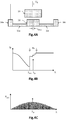
- the formation of dissipative solitons is detected from the evolution of the value of the transmission ratio Tr of the optoelectronic device 1.
- a detection waveguide 43 all or part of the output signal is received and then transmitted to a photodiode which provides the intensity of the detected optical signal.
- An oscilloscope records the value of the intensity of the detected signal as a function of the value of the bias voltage U. This gives a signal of the transmission rate Tr as a function of the bias voltage U.
- the spectral tuning device 4 applies a polarization voltage U in inverse to the semiconductor junction, whose value U, between the initial value and the equilibrium value U 0 , gradually decreases in absolute value. This results in a decrease in the width ZCE of the space charge area ( Figure 4A ), which reflects a progressive increase in carrier concentration in the semiconductor junction.
- the refractive index n gj (U) of the junction guide 30 is modified, which leads here to a decrease in the effective index n eff (U) associated with the supermode, and therefore a decrease in the resonance wavelength ⁇ res (U).
- the oscilloscope records the decrease of the transmission rate Tr (U) as the voltage U decreases in absolute value, which indicates that the spectral agreement between the pump signal and the resonant mode remains in the blue ( blue-detuning ) .
- the effective resonance wavelength ⁇ res (U ⁇ U ref ) becomes lower than the pump wavelength.
- ⁇ p that is to say that the spectral chord is in red ( red-detuning ), as illustrated by Figure 4B .
- the oscilloscope detects a stepwise increase in the transmission rate Tr (U), a sign that the solitonic regime is reached.
- Tr (U) the transmission rate
- the formation of dissipative solitons is indeed effective when the spectral agreement is in the red, insofar as the dispersion regime remains abnormal despite the presence of the junction guide 30.
- the dimensioning of the connecting guide 30 in particular its width l gj relative to that of the resonant ring 20, and the value of the distance d make it possible to keep the dispersion of the supermode abnormal.
- the spectral tuning device 4 stops the decrease of the bias voltage U.
- the value of the voltage is then between the reference value U ref and the equilibrium value U 0 .
- the number of solitons present in the resonant ring 20 can be controlled according to the value U of the applied bias voltage. More precisely, the incremental increase in the transmission rate reflects the decrease in the number of solitons present in the resonant ring 20. It is also possible to detect the full coherence of the frequency comb by comparing the spectral envelope of the frequency comb. generated vis-à-vis the function sinh 2 ( figure 4C ).
- a coherent frequency comb is obtained at the output 12 of the waveguide 10. It has a constant free spectral range, ie a constant spacing value between the successive frequency lines, as well as a low frequency and / or amplitude noise. Moreover, when a single dissipative soliton time travels through the resonant ring, the amplitude of the frequency lines is weighted by a spectral envelope of the hyperbolic sine squared (sinh 2 ) type centered on the wavelength ⁇ p of the pump. , thus translating the coherence of the frequency comb.
- the optoelectronic device 1 is thus able to achieve a spectral agreement between the pump signal and the resonant mode in the optical micro-resonator 3 to reach the solitonic regime Rs, and thus generate a quasi-coherent or coherent frequency comb.
- the spectral tuning device 4 does not include a tunable laser that is able to perform a sufficiently fine and precise scanning of the resonance.
- a tunable laser has the disadvantages of not being easily integrable at the support substrate and can be bulky. It may also not be precise enough, which may result in difficulty in addressing the solitonic regime. Indeed, as the show it figure 1D , the solitonic regime exists only for a narrow width of the resonance spectrum.
- the spectral agreement is ensured by keeping the pump wavelength ⁇ p substantially constant and using a junction guide positioned vis-à-vis the resonant ring 30 to allow the formation of a supermode, whose effective index is modified by the polarization of the semiconductor junction.
- the modification of the effective index, and therefore of the resonance wavelength ⁇ res of the supermode makes it possible to go from blue-detuning to red-detuning , a necessary condition for the formation of dissipative temporal solitons.
- the spectral tuning is simplified, fast and accurate, via a spectral tuning device easily integrable within a substrate, particularly SOI type.
- the resonant ring 20 when the resonant ring 20 is made of a III-V material with optical Kerr effect and the junction guide 30 is made of silicon, the resonant ring 20 has an abnormal dispersion regime for transverse dimensions of thickness and width such that it remains monomode. This makes it possible to avoid the presence of several optical modes in the resonant ring 20, whose possible interferences are likely to degrade the formation of dissipative time solitons of Kerr type.
- the optoelectronic device 1 may comprise a laser source 2 adapted to emit a monochromatic (continuous) pump optical signal of a wavelength substantially constant in time, for example equal to 1.55 ⁇ m.
- the pump signal is guided in the coupling waveguide 10, the latter being single-mode and supporting the fundamental mode TE 00 .
- the resonant ring 20 is made of AlGaAs which is a III-V material with an optical Kerr effect whose value of the non-linear index n2 is high.
- the optical power required to generate a frequency comb by mixing four cascaded waves is low, less than 10mW, and remains lower than the optical absorption power of two photons silicon forming the junction guide 30.
- It is based on a support layer 50 of silicon oxide SiO x , for example SiO 2 , and has a circle shape with a radius r of approximately 12.5 ⁇ m, a thickness e ga of approximately 400 nm and a width l ga of 630 nm. about.
- the resonant ring 20 is therefore monomode at 1.55 ⁇ m and here supports the fundamental mode TE 00 .
- the resonant ring 20 has a chromatic dispersion parameter D associated with the fundamental mode TE 00 at 1.55 ⁇ m equal to 764.2 ps / (nm.km) in the absence of a junction guide 30.
- the resonant ring 20 is surrounded by a sheath made here of silicon oxide SiO 2 .
- the junction guide 30 is made of Si. It is superimposed on the resonant ring 20 in the -Z direction, and has a circle shape with a radius of 12.5 ⁇ m also.
- the guide junction 30 has a thickness e gj of about 300 nm and the width l gj is about 280nm.
- the distance d separating the connecting guide 30 from the resonant ring 20 is about 100 nm.
- the semiconductor junction is reverse biased, thereby causing controlled depletion of carriers in the space charge region.
- the ZCE has an initial width l ZCE, init to U init which decreases with the decrease of the value U of the bias voltage (in absolute value).
- the value of the chromatic dispersion parameter D of the optical mode in the resonant ring 20 depends on the bias voltage U applied to the semiconductor junction.
- the parameter D varies between a value of 24 ps / (nm.km) at zero equilibrium voltage U 0 , and a value of 50 ps / (nm.km) at an initial U init voltage of -2,8V approx. It remains positive regardless of the value of the voltage U between U init and U 0 , thus reflecting the fact that the dispersion remains abnormal during the spectral tuning phase to obtain the solitonic regime.
- the presence of the junction guide 30 and the application of the bias voltage do not disturb the formation of the dissipative time solitons in the resonant ring 20.
- the Figure 5B illustrates an example of evolution of the value of the shift ⁇ v res resonance frequency as a function of the bias voltage U.
- the semiconductor junction is reverse biased, leading to carrier depletion.
- the frequency shift ⁇ v is here of the order of 550 MHz when the polarization voltage U reaches a value of -2.8V approximately.
- the resonant mode present in the aforementioned resonant ring 20 is the TE (transverse electric) mode but it could be the TM mode (transverse magnetic).
- the quality factor of the resonant ring 20 may be higher insofar as the supermode TM perceives only the roughness of the lower and upper faces of the waveguides since it oscillates along the Z axis and not in the XY plane.
- the lower and upper faces of the waveguides have a lower roughness, at least an order of magnitude, than that of the lateral flanks.
Landscapes
- Physics & Mathematics (AREA)
- Nonlinear Science (AREA)
- General Physics & Mathematics (AREA)
- Optics & Photonics (AREA)
- Optical Modulation, Optical Deflection, Nonlinear Optics, Optical Demodulation, Optical Logic Elements (AREA)
- Lasers (AREA)
Applications Claiming Priority (1)
| Application Number | Priority Date | Filing Date | Title |
|---|---|---|---|
| FR1752226A FR3064078B1 (fr) | 2017-03-17 | 2017-03-17 | Dispositif optoelectronique de generation d’un peigne de frequences |
Publications (2)
| Publication Number | Publication Date |
|---|---|
| EP3385784A1 true EP3385784A1 (de) | 2018-10-10 |
| EP3385784B1 EP3385784B1 (de) | 2023-01-11 |
Family
ID=59649783
Family Applications (1)
| Application Number | Title | Priority Date | Filing Date |
|---|---|---|---|
| EP18161911.5A Active EP3385784B1 (de) | 2017-03-17 | 2018-03-15 | Optoelektronische vorrichtung zur erzeugung eines frequenzkamms |
Country Status (3)
| Country | Link |
|---|---|
| US (1) | US10268100B2 (de) |
| EP (1) | EP3385784B1 (de) |
| FR (1) | FR3064078B1 (de) |
Cited By (2)
| Publication number | Priority date | Publication date | Assignee | Title |
|---|---|---|---|---|
| WO2020076402A1 (en) * | 2018-10-12 | 2020-04-16 | Imra America, Inc. | Compact microresonator frequency comb |
| US20220229346A1 (en) * | 2021-01-15 | 2022-07-21 | Nokia Solutions And Networks Oy | Dual-ring resonators for optical frequency comb generation |
Families Citing this family (22)
| Publication number | Priority date | Publication date | Assignee | Title |
|---|---|---|---|---|
| FR3061776B1 (fr) * | 2017-01-09 | 2019-05-31 | Commissariat A L'energie Atomique Et Aux Energies Alternatives | Dispositif optoelectronique de generation d’un peigne de frequences coherent |
| DE102017200755B3 (de) * | 2017-01-18 | 2018-03-08 | Leoni Kabel Gmbh | Sensorleitung, Messanordnung sowie Verfahren zur Erfassung einer Umgebungsvariablen |
| FR3084481B1 (fr) * | 2018-07-25 | 2021-07-23 | Commissariat Energie Atomique | Modulateur-commutateur athermique a deux anneaux superposes |
| FR3090909B1 (fr) | 2018-12-20 | 2021-05-07 | St Microelectronics Crolles 2 Sas | Dispositif électro-optique à résonateur en anneau |
| US11209597B2 (en) * | 2019-04-10 | 2021-12-28 | Ayar Labs, Inc. | Systems and methods for coupling light into a multi-mode resonator |
| US11221540B2 (en) * | 2019-09-17 | 2022-01-11 | Government Of The United States Of America, As Represented By The Secretary Of Commerce | Optical parametric oscillator and producing idler coherent light and signal coherent light from pump coherent light |
| EP4096509B1 (de) * | 2020-01-31 | 2026-03-25 | The General Hospital Corporation | Frequenzkammerzeugung basierend auf der basis einer elektrooptischen phasencode-modusverriegelung für oct mit kreisförmiger entfernungsmessung |
| US11226537B2 (en) * | 2020-02-06 | 2022-01-18 | Palo Alto Research Center Incorporated | Multi-layer optical device exhibiting anomalous dispersion |
| CN111969396B (zh) * | 2020-07-27 | 2021-07-27 | 中国科学院西安光学精密机械研究所 | 高集成中红外宽带超连续谱产生装置与方法 |
| US11940714B2 (en) | 2020-12-08 | 2024-03-26 | University Of Maryland, College Park | Ultra-low-noise, on-chip quantum devices |
| US11791902B2 (en) * | 2020-12-16 | 2023-10-17 | Mellanox Technologies, Ltd. | Heterogeneous integration of frequency comb generators for high-speed transceivers |
| NL2027948B1 (en) * | 2021-04-09 | 2022-10-20 | Univ Twente | Light source, mems optical switch, sensor and methods for manufacturing the same |
| SE545304C2 (en) * | 2021-07-08 | 2023-06-27 | Oskar Bjarki Helgason | An optical resonator frequency comb |
| CN114815045B (zh) * | 2022-03-07 | 2023-09-05 | 天津大学 | 一种基于二维材料纳米带的多模克尔光频梳产生器件 |
| CN116799601A (zh) * | 2022-03-17 | 2023-09-22 | 华为技术有限公司 | 一种光频梳生成设备、方法、光发射设备和光通信系统 |
| CN114978109B (zh) * | 2022-05-06 | 2024-12-03 | 中国人民解放军国防科技大学 | 一种基于模态耦合效应的频率调制方法、装置及谐振器 |
| GB2619566B (en) * | 2022-07-11 | 2024-07-03 | Orca Computing Ltd | Spectrally multiplexed single-photon emitter |
| WO2024157348A1 (ja) * | 2023-01-24 | 2024-08-02 | 日本電信電話株式会社 | 光デバイス |
| CN116667108B (zh) * | 2023-04-14 | 2026-03-24 | 中国航空工业集团公司北京长城计量测试技术研究所 | 一种光频梳自动恢复装置及方法 |
| US12572050B2 (en) * | 2023-07-11 | 2026-03-10 | Taiwan Semiconductor Manufacturing Company, Ltd. | Semiconductor device including optical ring waveguide |
| CN119890902B (zh) * | 2025-01-17 | 2026-04-03 | 南昌航空大学 | 一种基于氟化镁晶体微瓶腔的可调光频梳产生系统及方法 |
| CN119918018B (zh) * | 2025-04-07 | 2026-01-27 | 清华大学 | 空时谱智能全光可重构表征方法、架构与系统 |
Citations (1)
| Publication number | Priority date | Publication date | Assignee | Title |
|---|---|---|---|---|
| US20160011489A1 (en) * | 2013-02-28 | 2016-01-14 | Ecole Polytechnique Federale De Lausanne (Epfl) | Generating optical pulses via a soliton state of an optical microresonator |
Family Cites Families (5)
| Publication number | Priority date | Publication date | Assignee | Title |
|---|---|---|---|---|
| US8519803B2 (en) * | 2010-10-29 | 2013-08-27 | Hewlett-Packard Development Company, L.P. | Resonator systems and methods for tuning resonator systems |
| US9195113B2 (en) * | 2012-05-25 | 2015-11-24 | Honeywell International Inc. | Tunable multispectral laser source |
| US9490605B2 (en) * | 2013-04-22 | 2016-11-08 | Cornell University | Parametric comb generation via nonlinear wave mixing in high-Q optical resonator coupled to built-in laser resonator |
| CN110168444B (zh) * | 2016-10-31 | 2023-02-14 | 加利福尼亚大学董事会 | 绝热色散管理的频率梳产生 |
| FR3061776B1 (fr) * | 2017-01-09 | 2019-05-31 | Commissariat A L'energie Atomique Et Aux Energies Alternatives | Dispositif optoelectronique de generation d’un peigne de frequences coherent |
-
2017
- 2017-03-17 FR FR1752226A patent/FR3064078B1/fr not_active Expired - Fee Related
-
2018
- 2018-03-15 EP EP18161911.5A patent/EP3385784B1/de active Active
- 2018-03-16 US US15/923,571 patent/US10268100B2/en active Active
Patent Citations (1)
| Publication number | Priority date | Publication date | Assignee | Title |
|---|---|---|---|---|
| US20160011489A1 (en) * | 2013-02-28 | 2016-01-14 | Ecole Polytechnique Federale De Lausanne (Epfl) | Generating optical pulses via a soliton state of an optical microresonator |
Non-Patent Citations (7)
| Title |
|---|
| G. T. REED ET AL: "Silicon optical modulators", NATURE PHOTONICS, vol. 4, no. 8, 12 August 2010 (2010-08-12), UK, pages 518 - 526, XP055334361, ISSN: 1749-4885, DOI: 10.1038/nphoton.2010.179 * |
| HOJOONG JUNG ET AL: "Electrical tuning and switching of an optical frequency comb generated in aluminum nitride microring resonators", OPTICS LETTERS, OPTICAL SOCIETY OF AMERICA, vol. 39, no. 1, 1 January 2014 (2014-01-01), pages 84 - 87, XP001587372, ISSN: 0146-9592, [retrieved on 20131220], DOI: 10.1364/OL.39.000084 * |
| MOHAMMAD SOLTANI ET AL: "Enabling arbitrary wavelength frequency combs on chip : Enabling arbitrary wavelength frequency combs on chip", LASER & PHOTONICS REVIEWS, vol. 10, no. 1, 17 December 2015 (2015-12-17), DE, pages 158 - 162, XP055440273, ISSN: 1863-8880, DOI: 10.1002/lpor.201500226 * |
| STEVEN A. MILLER ET AL: "Tunable frequency combs based on dual microring resonators", OPTICS EXPRESS, vol. 23, no. 16, 7 August 2015 (2015-08-07), pages 21527, XP055410219, DOI: 10.1364/OE.23.021527 * |
| T. HERR ET AL: "Temporal solitons in optical microresonators", NATURE PHOTONICS, vol. 8, no. 2, 22 December 2013 (2013-12-22), UK, pages 145 - 152, XP055438896, ISSN: 1749-4885, DOI: 10.1038/nphoton.2013.343 * |
| XIAOXIAO XUE ET AL: "Thermal tuning of Kerr frequency combs in silicon nitride microring resonators", OPTICS EXPRESS, vol. 24, no. 1, 11 January 2016 (2016-01-11), pages 687, XP055440304, ISSN: 2161-2072, DOI: 10.1364/OE.24.000687 * |
| XUEZHI ZHANG ET AL: "Mid-infrared frequency comb generation in coupled silicon microring resonators", OPTICS COMMUNICATIONS, vol. 332, 1 December 2014 (2014-12-01), AMSTERDAM, NL, pages 125 - 131, XP055440192, ISSN: 0030-4018, DOI: 10.1016/j.optcom.2014.06.058 * |
Cited By (4)
| Publication number | Priority date | Publication date | Assignee | Title |
|---|---|---|---|---|
| WO2020076402A1 (en) * | 2018-10-12 | 2020-04-16 | Imra America, Inc. | Compact microresonator frequency comb |
| US11409185B2 (en) | 2018-10-12 | 2022-08-09 | Imra America, Inc. | Compact microresonator frequency comb |
| US20220229346A1 (en) * | 2021-01-15 | 2022-07-21 | Nokia Solutions And Networks Oy | Dual-ring resonators for optical frequency comb generation |
| US11402724B1 (en) * | 2021-01-15 | 2022-08-02 | Nokia Solutions And Networks Oy | Dual-ring resonators for optical frequency comb generation |
Also Published As
| Publication number | Publication date |
|---|---|
| FR3064078A1 (fr) | 2018-09-21 |
| US10268100B2 (en) | 2019-04-23 |
| US20180307118A1 (en) | 2018-10-25 |
| FR3064078B1 (fr) | 2020-07-24 |
| EP3385784B1 (de) | 2023-01-11 |
Similar Documents
| Publication | Publication Date | Title |
|---|---|---|
| EP3385784B1 (de) | Optoelektronische vorrichtung zur erzeugung eines frequenzkamms | |
| EP3346328B1 (de) | Optoelektronische vorrichtung zur erzeugung eines kohärenten frequenzkamms | |
| EP3190672B1 (de) | Laserquelle mit halbleiter | |
| EP0033048B1 (de) | Interferometer mit abstimmbarer optischer Höhlung, das eine optische monomoden Faser befasst, und dessen Anwendung zur Filtrierung und Spektrographie | |
| EP3425344B1 (de) | Bewegungssensor mit mikroresonator mit segmentiertem ring | |
| EP3404781B1 (de) | Quelle für geführtes licht, ihr herstellungsverfahren und ihre verwendung für die emission von einzelnen photonen | |
| EP3869160B1 (de) | Strukturierter faseroptischer sensor mit integrierter laser-emissionsvorrichtung mit abstimmbarem noniuseffekt | |
| EP0575227A1 (de) | Verfahren und Vorrichtung zur Modulation und Verstärkung von Lichtstrahlen | |
| EP3353502B1 (de) | Messsystem und temperatur und/oder formänderungssensor mit brillouinrückreflexionsanalyse | |
| EP2141520A1 (de) | Kupplungsvorrichtung mit kompensierter Doppelbrechung | |
| EP3428716B1 (de) | Optischer phasenmodulator mit sinusoidalem p-n-übergang | |
| WO2010000824A1 (fr) | Structure de guide d'onde optique micronanostructuré pour le contrôle de la biréfringence | |
| EP1125347B1 (de) | Auto-adaptierte filter zur verfeinerung der laseremission | |
| EP2476143B1 (de) | Lichtmischer zur erzeugung von terahertz-strahlung | |
| FR2647552A1 (fr) | Systeme de mesure de signaux electriques a l'aide d'impulsions optiques ultracourtes | |
| EP3764136A1 (de) | Verfahren zur herstellung eines adiabatischen modentransformators zwischen zwei wellenleitern | |
| EP2525200B1 (de) | Thermoelektrische Komponente mit plasmonischer Führung, die eine Messvorrichtung der gekoppelten Leistung im geführten Modus umfasst | |
| EP2818921B1 (de) | Vorrichtung zur nicht-linearen Signalumwandlung durch Vermischen von vier Wellen | |
| EP3469408B1 (de) | Optische vorrichtung | |
| EP1306941A1 (de) | Optische Resonator in Resonanz in einem kontinuerlichen Frequenzbereich | |
| EP3911999A1 (de) | Verfahren zum umsetzen der frequenz eines optischen signals durch mischen mehrerer wellen | |
| EP4034923B1 (de) | Optisches system und verfahren zu dessen herstellung | |
| EP3599501A1 (de) | Athermischer modulator-umschalter mit zwei übereinander angeordneten ringen | |
| FR2892514A1 (fr) | Detecteur d'ondes electromagnetiques a bande passante terahertz | |
| FR2887082A1 (fr) | Laser a semi-conducteur a tres faible bruit |
Legal Events
| Date | Code | Title | Description |
|---|---|---|---|
| PUAI | Public reference made under article 153(3) epc to a published international application that has entered the european phase |
Free format text: ORIGINAL CODE: 0009012 |
|
| STAA | Information on the status of an ep patent application or granted ep patent |
Free format text: STATUS: REQUEST FOR EXAMINATION WAS MADE |
|
| 17P | Request for examination filed |
Effective date: 20180315 |
|
| AK | Designated contracting states |
Kind code of ref document: A1 Designated state(s): AL AT BE BG CH CY CZ DE DK EE ES FI FR GB GR HR HU IE IS IT LI LT LU LV MC MK MT NL NO PL PT RO RS SE SI SK SM TR |
|
| AX | Request for extension of the european patent |
Extension state: BA ME |
|
| STAA | Information on the status of an ep patent application or granted ep patent |
Free format text: STATUS: EXAMINATION IS IN PROGRESS |
|
| 17Q | First examination report despatched |
Effective date: 20210608 |
|
| GRAP | Despatch of communication of intention to grant a patent |
Free format text: ORIGINAL CODE: EPIDOSNIGR1 |
|
| STAA | Information on the status of an ep patent application or granted ep patent |
Free format text: STATUS: GRANT OF PATENT IS INTENDED |
|
| INTG | Intention to grant announced |
Effective date: 20220801 |
|
| GRAS | Grant fee paid |
Free format text: ORIGINAL CODE: EPIDOSNIGR3 |
|
| GRAA | (expected) grant |
Free format text: ORIGINAL CODE: 0009210 |
|
| STAA | Information on the status of an ep patent application or granted ep patent |
Free format text: STATUS: THE PATENT HAS BEEN GRANTED |
|
| AK | Designated contracting states |
Kind code of ref document: B1 Designated state(s): AL AT BE BG CH CY CZ DE DK EE ES FI FR GB GR HR HU IE IS IT LI LT LU LV MC MK MT NL NO PL PT RO RS SE SI SK SM TR |
|
| REG | Reference to a national code |
Ref country code: GB Ref legal event code: FG4D Free format text: NOT ENGLISH |
|
| REG | Reference to a national code |
Ref country code: CH Ref legal event code: EP |
|
| REG | Reference to a national code |
Ref country code: DE Ref legal event code: R096 Ref document number: 602018045222 Country of ref document: DE |
|
| REG | Reference to a national code |
Ref country code: IE Ref legal event code: FG4D Free format text: LANGUAGE OF EP DOCUMENT: FRENCH |
|
| REG | Reference to a national code |
Ref country code: AT Ref legal event code: REF Ref document number: 1543777 Country of ref document: AT Kind code of ref document: T Effective date: 20230215 |
|
| REG | Reference to a national code |
Ref country code: LT Ref legal event code: MG9D |
|
| REG | Reference to a national code |
Ref country code: NL Ref legal event code: MP Effective date: 20230111 |
|
| REG | Reference to a national code |
Ref country code: AT Ref legal event code: MK05 Ref document number: 1543777 Country of ref document: AT Kind code of ref document: T Effective date: 20230111 |
|
| PG25 | Lapsed in a contracting state [announced via postgrant information from national office to epo] |
Ref country code: NL Free format text: LAPSE BECAUSE OF FAILURE TO SUBMIT A TRANSLATION OF THE DESCRIPTION OR TO PAY THE FEE WITHIN THE PRESCRIBED TIME-LIMIT Effective date: 20230111 |
|
| PG25 | Lapsed in a contracting state [announced via postgrant information from national office to epo] |
Ref country code: RS Free format text: LAPSE BECAUSE OF FAILURE TO SUBMIT A TRANSLATION OF THE DESCRIPTION OR TO PAY THE FEE WITHIN THE PRESCRIBED TIME-LIMIT Effective date: 20230111 Ref country code: PT Free format text: LAPSE BECAUSE OF FAILURE TO SUBMIT A TRANSLATION OF THE DESCRIPTION OR TO PAY THE FEE WITHIN THE PRESCRIBED TIME-LIMIT Effective date: 20230511 Ref country code: NO Free format text: LAPSE BECAUSE OF FAILURE TO SUBMIT A TRANSLATION OF THE DESCRIPTION OR TO PAY THE FEE WITHIN THE PRESCRIBED TIME-LIMIT Effective date: 20230411 Ref country code: LV Free format text: LAPSE BECAUSE OF FAILURE TO SUBMIT A TRANSLATION OF THE DESCRIPTION OR TO PAY THE FEE WITHIN THE PRESCRIBED TIME-LIMIT Effective date: 20230111 Ref country code: LT Free format text: LAPSE BECAUSE OF FAILURE TO SUBMIT A TRANSLATION OF THE DESCRIPTION OR TO PAY THE FEE WITHIN THE PRESCRIBED TIME-LIMIT Effective date: 20230111 Ref country code: HR Free format text: LAPSE BECAUSE OF FAILURE TO SUBMIT A TRANSLATION OF THE DESCRIPTION OR TO PAY THE FEE WITHIN THE PRESCRIBED TIME-LIMIT Effective date: 20230111 Ref country code: ES Free format text: LAPSE BECAUSE OF FAILURE TO SUBMIT A TRANSLATION OF THE DESCRIPTION OR TO PAY THE FEE WITHIN THE PRESCRIBED TIME-LIMIT Effective date: 20230111 Ref country code: AT Free format text: LAPSE BECAUSE OF FAILURE TO SUBMIT A TRANSLATION OF THE DESCRIPTION OR TO PAY THE FEE WITHIN THE PRESCRIBED TIME-LIMIT Effective date: 20230111 |
|
| PG25 | Lapsed in a contracting state [announced via postgrant information from national office to epo] |
Ref country code: SE Free format text: LAPSE BECAUSE OF FAILURE TO SUBMIT A TRANSLATION OF THE DESCRIPTION OR TO PAY THE FEE WITHIN THE PRESCRIBED TIME-LIMIT Effective date: 20230111 Ref country code: PL Free format text: LAPSE BECAUSE OF FAILURE TO SUBMIT A TRANSLATION OF THE DESCRIPTION OR TO PAY THE FEE WITHIN THE PRESCRIBED TIME-LIMIT Effective date: 20230111 Ref country code: IS Free format text: LAPSE BECAUSE OF FAILURE TO SUBMIT A TRANSLATION OF THE DESCRIPTION OR TO PAY THE FEE WITHIN THE PRESCRIBED TIME-LIMIT Effective date: 20230511 Ref country code: GR Free format text: LAPSE BECAUSE OF FAILURE TO SUBMIT A TRANSLATION OF THE DESCRIPTION OR TO PAY THE FEE WITHIN THE PRESCRIBED TIME-LIMIT Effective date: 20230412 Ref country code: FI Free format text: LAPSE BECAUSE OF FAILURE TO SUBMIT A TRANSLATION OF THE DESCRIPTION OR TO PAY THE FEE WITHIN THE PRESCRIBED TIME-LIMIT Effective date: 20230111 |
|
| REG | Reference to a national code |
Ref country code: DE Ref legal event code: R097 Ref document number: 602018045222 Country of ref document: DE |
|
| PG25 | Lapsed in a contracting state [announced via postgrant information from national office to epo] |
Ref country code: SM Free format text: LAPSE BECAUSE OF FAILURE TO SUBMIT A TRANSLATION OF THE DESCRIPTION OR TO PAY THE FEE WITHIN THE PRESCRIBED TIME-LIMIT Effective date: 20230111 Ref country code: RO Free format text: LAPSE BECAUSE OF FAILURE TO SUBMIT A TRANSLATION OF THE DESCRIPTION OR TO PAY THE FEE WITHIN THE PRESCRIBED TIME-LIMIT Effective date: 20230111 Ref country code: MC Free format text: LAPSE BECAUSE OF FAILURE TO SUBMIT A TRANSLATION OF THE DESCRIPTION OR TO PAY THE FEE WITHIN THE PRESCRIBED TIME-LIMIT Effective date: 20230111 Ref country code: EE Free format text: LAPSE BECAUSE OF FAILURE TO SUBMIT A TRANSLATION OF THE DESCRIPTION OR TO PAY THE FEE WITHIN THE PRESCRIBED TIME-LIMIT Effective date: 20230111 Ref country code: DK Free format text: LAPSE BECAUSE OF FAILURE TO SUBMIT A TRANSLATION OF THE DESCRIPTION OR TO PAY THE FEE WITHIN THE PRESCRIBED TIME-LIMIT Effective date: 20230111 Ref country code: CZ Free format text: LAPSE BECAUSE OF FAILURE TO SUBMIT A TRANSLATION OF THE DESCRIPTION OR TO PAY THE FEE WITHIN THE PRESCRIBED TIME-LIMIT Effective date: 20230111 |
|
| REG | Reference to a national code |
Ref country code: CH Ref legal event code: PL |
|
| PLBE | No opposition filed within time limit |
Free format text: ORIGINAL CODE: 0009261 |
|
| STAA | Information on the status of an ep patent application or granted ep patent |
Free format text: STATUS: NO OPPOSITION FILED WITHIN TIME LIMIT |
|
| PG25 | Lapsed in a contracting state [announced via postgrant information from national office to epo] |
Ref country code: SK Free format text: LAPSE BECAUSE OF FAILURE TO SUBMIT A TRANSLATION OF THE DESCRIPTION OR TO PAY THE FEE WITHIN THE PRESCRIBED TIME-LIMIT Effective date: 20230111 |
|
| REG | Reference to a national code |
Ref country code: BE Ref legal event code: MM Effective date: 20230331 |
|
| 26N | No opposition filed |
Effective date: 20231012 |
|
| PG25 | Lapsed in a contracting state [announced via postgrant information from national office to epo] |
Ref country code: LU Free format text: LAPSE BECAUSE OF NON-PAYMENT OF DUE FEES Effective date: 20230315 |
|
| REG | Reference to a national code |
Ref country code: IE Ref legal event code: MM4A |
|
| PG25 | Lapsed in a contracting state [announced via postgrant information from national office to epo] |
Ref country code: SI Free format text: LAPSE BECAUSE OF FAILURE TO SUBMIT A TRANSLATION OF THE DESCRIPTION OR TO PAY THE FEE WITHIN THE PRESCRIBED TIME-LIMIT Effective date: 20230111 Ref country code: LI Free format text: LAPSE BECAUSE OF NON-PAYMENT OF DUE FEES Effective date: 20230331 Ref country code: IE Free format text: LAPSE BECAUSE OF NON-PAYMENT OF DUE FEES Effective date: 20230315 Ref country code: CH Free format text: LAPSE BECAUSE OF NON-PAYMENT OF DUE FEES Effective date: 20230331 |
|
| PG25 | Lapsed in a contracting state [announced via postgrant information from national office to epo] |
Ref country code: BE Free format text: LAPSE BECAUSE OF NON-PAYMENT OF DUE FEES Effective date: 20230331 |
|
| PG25 | Lapsed in a contracting state [announced via postgrant information from national office to epo] |
Ref country code: IT Free format text: LAPSE BECAUSE OF FAILURE TO SUBMIT A TRANSLATION OF THE DESCRIPTION OR TO PAY THE FEE WITHIN THE PRESCRIBED TIME-LIMIT Effective date: 20230111 |
|
| PG25 | Lapsed in a contracting state [announced via postgrant information from national office to epo] |
Ref country code: BG Free format text: LAPSE BECAUSE OF FAILURE TO SUBMIT A TRANSLATION OF THE DESCRIPTION OR TO PAY THE FEE WITHIN THE PRESCRIBED TIME-LIMIT Effective date: 20230111 |
|
| PG25 | Lapsed in a contracting state [announced via postgrant information from national office to epo] |
Ref country code: BG Free format text: LAPSE BECAUSE OF FAILURE TO SUBMIT A TRANSLATION OF THE DESCRIPTION OR TO PAY THE FEE WITHIN THE PRESCRIBED TIME-LIMIT Effective date: 20230111 |
|
| PG25 | Lapsed in a contracting state [announced via postgrant information from national office to epo] |
Ref country code: CY Free format text: LAPSE BECAUSE OF FAILURE TO SUBMIT A TRANSLATION OF THE DESCRIPTION OR TO PAY THE FEE WITHIN THE PRESCRIBED TIME-LIMIT; INVALID AB INITIO Effective date: 20180315 |
|
| PG25 | Lapsed in a contracting state [announced via postgrant information from national office to epo] |
Ref country code: HU Free format text: LAPSE BECAUSE OF FAILURE TO SUBMIT A TRANSLATION OF THE DESCRIPTION OR TO PAY THE FEE WITHIN THE PRESCRIBED TIME-LIMIT; INVALID AB INITIO Effective date: 20180315 |
|
| PG25 | Lapsed in a contracting state [announced via postgrant information from national office to epo] |
Ref country code: TR Free format text: LAPSE BECAUSE OF FAILURE TO SUBMIT A TRANSLATION OF THE DESCRIPTION OR TO PAY THE FEE WITHIN THE PRESCRIBED TIME-LIMIT Effective date: 20230111 |
|
| PGFP | Annual fee paid to national office [announced via postgrant information from national office to epo] |
Ref country code: GB Payment date: 20260324 Year of fee payment: 9 |
|
| PGFP | Annual fee paid to national office [announced via postgrant information from national office to epo] |
Ref country code: DE Payment date: 20260320 Year of fee payment: 9 |
|
| PGFP | Annual fee paid to national office [announced via postgrant information from national office to epo] |
Ref country code: FR Payment date: 20260318 Year of fee payment: 9 |