EP3425344B1 - Bewegungssensor mit mikroresonator mit segmentiertem ring - Google Patents
Bewegungssensor mit mikroresonator mit segmentiertem ring Download PDFInfo
- Publication number
- EP3425344B1 EP3425344B1 EP18181241.3A EP18181241A EP3425344B1 EP 3425344 B1 EP3425344 B1 EP 3425344B1 EP 18181241 A EP18181241 A EP 18181241A EP 3425344 B1 EP3425344 B1 EP 3425344B1
- Authority
- EP
- European Patent Office
- Prior art keywords
- micro
- resonator
- waveguide
- optical sensor
- waveguides
- Prior art date
- Legal status (The legal status is an assumption and is not a legal conclusion. Google has not performed a legal analysis and makes no representation as to the accuracy of the status listed.)
- Active
Links
Images


Classifications
-
- G—PHYSICS
- G01—MEASURING; TESTING
- G01C—MEASURING DISTANCES, LEVELS OR BEARINGS; SURVEYING; NAVIGATION; GYROSCOPIC INSTRUMENTS; PHOTOGRAMMETRY OR VIDEOGRAMMETRY
- G01C19/00—Gyroscopes; Turn-sensitive devices using vibrating masses; Turn-sensitive devices without moving masses; Measuring angular rate using gyroscopic effects
- G01C19/58—Turn-sensitive devices without moving masses
- G01C19/64—Gyrometers using the Sagnac effect, i.e. rotation-induced shifts between counter-rotating electromagnetic beams
- G01C19/72—Gyrometers using the Sagnac effect, i.e. rotation-induced shifts between counter-rotating electromagnetic beams with counter-rotating light beams in a passive ring, e.g. fibre laser gyrometers
- G01C19/727—Gyrometers using the Sagnac effect, i.e. rotation-induced shifts between counter-rotating electromagnetic beams with counter-rotating light beams in a passive ring, e.g. fibre laser gyrometers using a passive ring resonator
-
- G—PHYSICS
- G01—MEASURING; TESTING
- G01D—MEASURING NOT SPECIALLY ADAPTED FOR A SPECIFIC VARIABLE; ARRANGEMENTS FOR MEASURING TWO OR MORE VARIABLES NOT COVERED IN A SINGLE OTHER SUBCLASS; TARIFF METERING APPARATUS; MEASURING OR TESTING NOT OTHERWISE PROVIDED FOR
- G01D5/00—Mechanical means for transferring the output of a sensing member; Means for converting the output of a sensing member to another variable where the form or nature of the sensing member does not constrain the means for converting; Transducers not specially adapted for a specific variable
- G01D5/26—Mechanical means for transferring the output of a sensing member; Means for converting the output of a sensing member to another variable where the form or nature of the sensing member does not constrain the means for converting; Transducers not specially adapted for a specific variable characterised by optical transfer means, i.e. using infrared, visible, or ultraviolet light
- G01D5/32—Mechanical means for transferring the output of a sensing member; Means for converting the output of a sensing member to another variable where the form or nature of the sensing member does not constrain the means for converting; Transducers not specially adapted for a specific variable characterised by optical transfer means, i.e. using infrared, visible, or ultraviolet light with attenuation or whole or partial obturation of beams of light
- G01D5/34—Mechanical means for transferring the output of a sensing member; Means for converting the output of a sensing member to another variable where the form or nature of the sensing member does not constrain the means for converting; Transducers not specially adapted for a specific variable characterised by optical transfer means, i.e. using infrared, visible, or ultraviolet light with attenuation or whole or partial obturation of beams of light the beams of light being detected by photocells
- G01D5/353—Mechanical means for transferring the output of a sensing member; Means for converting the output of a sensing member to another variable where the form or nature of the sensing member does not constrain the means for converting; Transducers not specially adapted for a specific variable characterised by optical transfer means, i.e. using infrared, visible, or ultraviolet light with attenuation or whole or partial obturation of beams of light the beams of light being detected by photocells influencing the transmission properties of an optical fibre
- G01D5/35338—Mechanical means for transferring the output of a sensing member; Means for converting the output of a sensing member to another variable where the form or nature of the sensing member does not constrain the means for converting; Transducers not specially adapted for a specific variable characterised by optical transfer means, i.e. using infrared, visible, or ultraviolet light with attenuation or whole or partial obturation of beams of light the beams of light being detected by photocells influencing the transmission properties of an optical fibre using other arrangements than interferometer arrangements
-
- G—PHYSICS
- G02—OPTICS
- G02B—OPTICAL ELEMENTS, SYSTEMS OR APPARATUS
- G02B6/00—Light guides; Structural details of arrangements comprising light guides and other optical elements, e.g. couplings
- G02B6/24—Coupling light guides
- G02B6/26—Optical coupling means
- G02B6/28—Optical coupling means having data bus means, i.e. plural waveguides interconnected and providing an inherently bidirectional system by mixing and splitting signals
- G02B6/293—Optical coupling means having data bus means, i.e. plural waveguides interconnected and providing an inherently bidirectional system by mixing and splitting signals with wavelength selective means
- G02B6/29331—Optical coupling means having data bus means, i.e. plural waveguides interconnected and providing an inherently bidirectional system by mixing and splitting signals with wavelength selective means operating by evanescent wave coupling
- G02B6/29335—Evanescent coupling to a resonator cavity, i.e. between a waveguide mode and a resonant mode of the cavity
- G02B6/29338—Loop resonators
- G02B6/29341—Loop resonators operating in a whispering gallery mode evanescently coupled to a light guide, e.g. sphere or disk or cylinder
Definitions
- the invention relates to the field of waveguide micro-resonators, and their use for detecting, or even measuring, a deformation of the micro-resonator or a movement in the near field of this micro-resonator.
- the waveguide micro-resonator consists of a curved ring-shaped waveguide, called a ring micro-resonator.
- the ring micro-resonator has no sheath. It is the surrounding environment which acts as a sheath.
- This micro-resonator is coupled to an injection and extraction waveguide, by evanescent coupling.
- Evanescent coupling corresponds to an interaction between a guided mode of the injection and extraction waveguide, and a guided mode of the micro-resonator, which results in an energy transfer between these two modes.
- a resonance wavelength of the micro-resonator is a wavelength for which the phase shift provided by a turn in the ring is a multiple of 2 ⁇ .
- a light beam is sent to the input of the injection and extraction waveguide.
- Part of the analysis laser beam escapes towards the micro-resonator, where it performs one or more turns before returning to the injection and extraction waveguide.
- the part of the analysis beam passing through the micro-resonator undergoes optical losses there, due in particular to absorption by the surrounding medium.
- a mobile nanobeam is placed in the near field of the micro-resonator. It approaches or moves away from the micro-resonator, depending on external conditions.
- the position of the nanobeam locally defines the composition of a cladding for the micro-resonator. This position therefore influences the value of the effective index N eff of the guided mode in the micro-resonator, and consequently the values of the resonance wavelength ⁇ .
- the analysis of a variation of the light, at the output of the injection and extraction waveguide, therefore makes it possible to detect and measure a variation in the position of the nanobeam, relative to the ring micro-resonator.
- An objective of the present invention is to provide an optical sensor comprising a waveguide micro-resonator, offering improved sensitivity to the detection of a movement in the near field of this micro-resonator.
- the micro-resonator consists of a plurality of elementary waveguides, spaced apart from one another, and arranged one after the other in a loop-shaped arrangement.
- the term “loop” designates here any curved line which closes on itself, preferably without crossing, for example a circle (or ring, considering all the volume occupied by the elementary waveguides), an angled triangle rounded, a rectangle with rounded angles, two semicircles joined by two parallel segments, etc.
- an additional mobile element such as a nanobeam, can move close to the micro-resonator, until it is between two elementary waveguides.
- the additional mobile element When the additional mobile element is located between two elementary waveguides, it cuts the optical path of the light beam propagating in the micro-resonator, which results in a sharp increase in losses at the resonance wavelengths of the micro-resonator and / or a strong phase modification in the micro-resonator.
- the constitution of the micro-resonator in elementary waveguides spaced from one another has other advantages, some of which are detailed below.
- a waveguide micro-resonator can, in particular when it is arranged suspended, contract and extend radially. This movement is called "micro-resonator breathing”.
- This movement changes the curvilinear length of the micro-resonator, which results in a change in its resonant wavelengths.
- this movement also modifies the length of the gap between two neighboring elementary waveguides, and therefore the effective index of a guided mode in the micro-resonator.
- the resonance length is also a function of this effective index.
- the variation in resonance wavelength is therefore higher, for the same amplitude of radial movement.
- micro-resonator is made up of separate elementary waveguides, it is possible to free the movement of some of them, relative to the others.
- the movement within the optical device designates a deformation of the micro-resonator itself, and / or the movement of a movable element relative to the micro-resonator.
- the analysis device can in particular be designed to compare a spectrum in wavelength, supplied by the photo-detector at a current instant t1, and a reference spectrum.
- the reference spectrum can be a wavelength spectrum, supplied by the photo-detector at an instant t0 preceding the instant t1.
- the comparison of spectra may include a comparison of intensity values, in local minima of these spectra, and / or a comparison of associated wavelength values. to these local minima.
- the invention is based on the interaction between a mechanical displacement and an optical phenomenon of resonance.
- the optical sensor according to the invention therefore forms an opto-mechanical sensor, with improved sensitivity.
- the improvement is linked to an exacerbated opto-mechanical coupling between the mechanical displacement and the optical phenomenon of resonance, or in other words between a mechanical oscillator and an optical oscillator.
- the optical sensor according to the invention offers increased sensitivity to the measurement of nanometric displacements.
- the optical device comprising the micro-resonator is described in detail, and protected as such, in the patent application FR 16 57222 , filed on July 27, 2016.
- This patent application does not describe an optical sensor comprising an analysis device as described above, and does not identify the advantages specific to a use of said optical device to obtain information relating to a trip.
- the optical sensor according to the invention can also comprise an annex mobile element, adapted to move relative to the micro-resonator so as to pass through partially or totally a free space between two neighboring elementary waveguides.
- the elementary waveguides of the micro-resonator can be suspended above a substrate, and around a pedestal.
- the pedestal has the shape of a cylinder, the base of the cylinder having a diameter of between 0.25 and 0.75 times the diameter of the micro-resonator.
- the elementary waveguides of the micro-resonator are mounted integral with a support plate, itself resting on the pedestal.
- the support plate may have one or more trenches, each of these trenches extending from a peripheral region of the support plate, located between two neighboring elementary waveguides, to a central region of the support plate.
- the support plate can have at least one pair of trenches, each pair delimiting on the support plate a so-called zone, receiving one or more elementary waveguides.
- the support plate can have a single pair of trenches.
- the support plate may have two pairs of trenches, arranged symmetrical to one another.
- the support plate may have a plurality of trenches together delimiting a plurality of isolated areas that are symmetrical in pairs.
- the elementary waveguides are suspended around the pedestal, by means of arms which extend in a plane parallel to the plane of the micro-resonator.
- the elementary waveguides can also be supported on a substrate, without a lever arm.
- the elementary waveguides of the micro-resonator are advantageously distributed periodically one after the other, according to a regular pitch called a distribution pitch.
- the figures 1A and 1B illustrate a first embodiment of an optical device 100 and an optical sensor 1000 according to the invention, respectively in a top view, in the plane (xOy) of an orthonormal coordinate system, and in a sectional view, in the plane (yOz) of the same coordinate system.
- the section plane AA ' corresponds to the figure 1B .
- the waveguide micro-resonator 120 consists of a plurality of waveguide sections, called elementary waveguides 121.
- the elementary waveguides 121 together define the optical path 123 traversed by the light in the micro-resonator, here a circular optical path 123 (shown in dotted lines on the diagram. figure 1A ). In other words, they are arranged one after the other in a ring-shaped arrangement.
- the several elementary waveguides are spaced from each other.
- the input of an elementary waveguide is not in direct physical contact with the output of a neighboring elementary waveguide.
- the elementary waveguides are separated in pairs by a respective free space 122.
- Each of the elementary waveguides 121 has no sheath, so that in operation, a surrounding medium around the micro-resonator 120 acts as a sheath.
- Each elementary waveguide 121 is advantageously made of the same and unique material (or alloy). This material is the same for all the elementary waveguides 121.
- the elementary waveguides are advantageously made of silicon or of silicon nitride.
- They are for example made of silicon, to guide a light beam in the infrared (wavelength greater than 1 ⁇ m, in particular between 1 ⁇ m and 10 ⁇ m).
- the elementary waveguides 121 are made of nitride, in particular silicon nitride (Si 3 N 4 ), to guide a light beam in the visible (wavelength strictly less than 1 ⁇ m, in particular between 0.4 ⁇ m and 0.8 ⁇ m).
- the micro-resonator 120 forms a segmented ring micro-resonator, that is to say a micro-resonator as described in the introduction, in which only certain sections of the curved waveguide are preserved, and form the elementary waveguides.
- the micro-resonator 120 is placed near the injection and extraction waveguide 110.
- the injection and extraction waveguide 110 extends in a straight line, parallel to a tangent to the micro-resonator.
- the injection and extraction waveguide 110 extends outside the micro-resonator 120, without necessarily having direct physical contact therewith.
- the injection and extraction waveguide 110 is made, like the elementary waveguides 121, of a single material (or alloy), the surrounding medium acting as a sheath.
- This single material is advantageously the same as that constituting the elementary waveguides.
- the injection and extraction waveguide is advantageously formed unsuspended, mechanically stable relative to the micro-resonator.
- micro-resonator 120 and the injection and extraction waveguide 110 are optically coupled to each other by evanescent coupling.
- the injection and extraction waveguide 110 receives as input a light beam 111 called the analysis beam.
- At least part of the analysis beam is transferred into the micro-resonator 120, by evanescent coupling.
- This part of the analysis beam is a signal at a resonant wavelength of the micro-resonator 120. It may be all or part of the analysis beam.
- a resonance wavelength of the micro-resonator is a wavelength for which the phase shift provided by one turn in the micro-resonator is a multiple of 2 ⁇ .
- This part of the analysis beam transferred from the injection and extraction waveguide 110 to the micro-resonator 120, makes several turns in the micro-resonator 120 before returning to the same injection waveguide and extraction 110.
- the thicknesses H and h 1 are measured along the axis (Oz), orthogonal to the plane of the micro-resonator.
- the thickness H is greater than or equal to the thickness h 1 .
- the flat support 140 extends under the set of elementary waveguides 121, between these elementary waveguides 121 and a substrate 172.
- the flat support 140 is in direct physical contact, on one side with each of the elementary waveguides 121, and on the other with said substrate 172.
- the micro-resonator 120 is not suspended above this substrate 172.
- the support points of an elementary waveguide 121 on the substrate 172 are aligned with said guide d. elementary wave, along the axis (Oz).
- the elementary waveguides 121 bear on the substrate 172, without a lever arm.
- the elementary waveguides are therefore mechanically stable, with respect to each other, and with respect to the substrate 172.
- the optical device 100 further comprises an annex movable element 130, able to move relative to the micro-resonator 120, preferably according to an oscillating movement.
- the elementary waveguides 121 are preferably wider than they are high (dimension according to (Oz)). .
- the movable arrangement of the element 130 can be achieved by a suspended fixing, one end of the element 130 being able to be left free.
- the additional mobile element 130 is located in the near field of the micro-resonator, spaced from the latter by a distance less than a few hundred nanometers, for example less than 600 nm and even less than 300 nm.
- At least one of the dimensions of the mobile annex element is less than 0.5 ⁇ m, preferably between 10 nm and 300 nm.
- the additional mobile element 130 is here a nanobeam, of width L1 of between 100 nm and 200 nm, and of length L2 of approximately 1 ⁇ m.
- the thickness of the nanobeam 130 (along the axis (Oz)) is less than that of the elementary waveguides 121, without this example being limiting.
- the nanobeam is movable between two extreme positions.
- the nanobeam 130 is shown twice, in each of these two extreme positions.
- the path 131 followed by the nanobeam, between these two extreme positions, is represented by a dotted arrow.
- the path 131 extends here in a plane parallel to the plane of the micro-resonator 120. It defines here a radius of the micro-resonator 120.
- the plane of the micro-resonator is a plane receiving the upper faces of the elementary waveguides 121, parallel to the plane (Oxy).
- the nanobeam 130 is oriented towards the center of the micro-resonator, but located entirely outside the latter.
- the optical losses in the micro-resonator remain limited.
- the nanobeam only interacts with the evanescent part of the beam circulating in the micro-resonator, as in the prior art.
- the nanobeam 130 has been translated along the path 131, and extends partly in a free space 122, between two neighboring elementary waveguides 121.
- optical losses increase with a rate of occupation, by the nanobeam, of a free space 122 between two elementary waveguides.
- the nanobeam can move according to an oscillating movement, during which it enters and leaves a free space 122, between two neighboring elementary waveguides 121.
- the photo-detector 150 includes at least one photodiode. It can also comprise spectral dispersion means such as a prism or a grating, or a simple filter, to distribute the different spectral components of a broad spectrum beam over the different photodiodes of a strip of photodiodes.
- spectral dispersion means such as a prism or a grating, or a simple filter, to distribute the different spectral components of a broad spectrum beam over the different photodiodes of a strip of photodiodes.
- It is arranged at one of the ends of the injection and extraction waveguide, to receive the beam 112 emerging from the injection and extraction waveguide 110, and resulting from the coupling between the micro-resonator 120 and the injection and extraction waveguide 110.
- the analysis device 160 comprises electronic and / or computer means, in particular a processor.
- This signal is advantageously, but in a nonlimiting manner, in the form of a wavelength spectrum of the beam 112, emerging from the injection and extraction waveguide 110.
- the analysis device 160 comprises in particular a comparator, electronic or computer, to compare the signal supplied by the photo-detector 150 with reference data, and to deduce therefrom information l d relating to a movement within the optical device. 100.
- the information l d is supplied at the output of the analysis device 160.
- the analysis device 160 implements in particular a comparison between a first wavelength spectrum, supplied by the photo-detector 150 at an initial instant t0, and a second wavelength spectrum, supplied by the photo-detector 150 to an instant t1 subsequent to t0.
- the wavelength spectrum, supplied at the initial time t0, then forms the reference data.
- the x-axis is a wavelength, in ⁇ m.
- the ordinate axis is a transmission rate from one end of the injection and extraction waveguide 110 to the other.
- the micro-resonator 120 consists of 500 elementary guides 121 made of silicon, bathed in air.
- the distribution pitch of the elementary guides 121 is 40 nm. They are distributed in a ring with a median radius equal to 5 ⁇ m.
- the injection and extraction waveguide has a section of 500 nm by 220 nm.
- the gap between the injection and extraction waveguide 110 and the micro-resonator 120 is 300 nm.
- the nanobeam is a rectangular parallelepiped with dimensions of 1000 nm x 220 nm x 30 nm.
- the spectra 20 and 21 each correspond to the analysis beam, minus the losses in the micro-resonator 120. These losses are localized at the resonance wavelengths of the micro-resonator 120. These losses form transmission minima 20 1 , 20 2 ... 20 i , respectively 21 1 , 21 2 ... 21 i , on spectra 20, respectively 21.
- the losses are much higher when the nanobeam 130 cuts the optical path of the beam passing through the micro-resonator.
- the transmission rate at the smallest resonance wavelength is reduced by approximately 8%, when the nanobeam 130 cuts the optical path of the beam passing through the micro-resonator.
- the evolution over time of the spectrum of the signal at the output of the injection and extraction waveguide makes it possible to detect with very good sensitivity that the nanobeam enters or leaves a free space between two guides. of neighboring elementary waves.
- the information, l d relating to a displacement within the optical device 100, may consist of the simple detection of a displacement greater than a predetermined threshold.
- the analysis device 160 uses the result of the comparison, here a comparison of spectra, to calculate the value of this displacement (in units of length).
- the information, l d then comprises this value of this displacement.
- Each displacement can be considered as a sum of two displacements, a first displacement where the nanobeam remains entirely outside the micro-resonator, and a second displacement where the nanobeam passes through an increasingly large portion of a free space between two elementary waveguides.
- the first movement can resume calculations implemented in the prior art.
- the second displacement involves original calculations, based on simulations or on a theoretical model of the micro-resonator.
- the nanobeam 130 can move along a vertical path 331, orthogonal to the plane of the micro-resonator 120, as illustrated in figure 3 .
- the width of the elementary waveguides is not representative, the latter preferably being wider than they are high.
- the additional mobile element is a membrane.
- the injection and extraction waveguide 110 is replaced by an injection waveguide 110A, to inject the analysis beam 111 into the micro-resonator, and a waveguide d 'separate extraction 110B from the injection waveguide, to receive what remains of the analysis beam after transit through the micro-resonator 120.
- This variant is illustrated by the optical device 100 'and the optical sensor 1000' of the figure 4 . To the figure 4 , the nanobeam is not shown.
- the analysis beam 111 can be a monochromatic beam, at a resonant wavelength of the micro-resonator 120, and the photo-detector 150 can consist of a simple photodiode, sensitive to this length d 'wave.
- the signal supplied by the photo-detector 150 to the analysis device 160 is not a spectrum but a single value of light intensity.
- the comparison implemented within the analysis device is then a comparison between an intensity value measured at the instant t1, and a reference value.
- Said reference value can be constituted by an intensity value measured at an instant t0, preceding the instant t1.
- This variant has the advantage that the photo-detector 150 receives only the wavelength affected by a displacement. It therefore offers increased sensitivity to this displacement, provided that the resonance wavelength is known, and little affected by the displacement.
- the optical device according to the invention does not include an additional mobile element, and the displacement of the injection and extraction waveguide, respectively of the injection waveguide and / or of the injection waveguide, is detected. waveguide extraction. Said waveguide is then advantageously arranged suspended, resting on at least two pillars.
- the optical device according to the invention on the contrary comprises several additional mobile elements such as nanobeams. These several elements move together, and together have a greater influence on the signal variations at the output of the injection and extraction waveguide. The sensitivity to a stress at the origin of these displacements is thus increased.
- the micro-resonator is arranged suspended, but its vibration modes are unlikely to modify the signal passing through the micro-resonator.
- the reference data are advantageously data previously measured by the photo-detector 150. It may also be data previously calculated, obtained entirely theoretically, or from compiled experimental measurements. during a preliminary calibration step.
- the optical device according to the invention can be placed inside a hermetic cavity put under vacuum. It can also be placed within a cryostat, to limit Brownian thermal displacement noise. It is, however, preferably subjected to atmospheric pressure.
- the optical sensor according to the invention may include the light source suitable for the emission of the analysis beam 111.
- the elementary waveguides may have the shape of a rectangular parallelepiped.
- the distribution pitch of the elementary waveguides 121 being reduced, preferably less than 2 ⁇ m, the optical path of the light guided in the micro-resonator 120 can be likened to a circular path.
- the micro-resonator here in the form of a ring, advantageously has an external radius less than or equal to 10 ⁇ m, in particular less than or equal to 5 ⁇ m.
- all the elementary waveguides have the same shape and the same dimensions.
- the shape of an elementary waveguide 121 is here a portion of a right cylinder with an annular base, this portion being delimited by two planes 124 receiving the generatrix of the cylinder and together defining an angle ⁇ .
- Each elementary waveguide 121 is characterized by a height, a width w and a length l (here l is a curvilinear length, measured at the center of the elementary waveguide).
- the various elementary waveguides 121 are distributed periodically one after the other, according to a regular pitch P , called a distribution pitch.
- the pitch P denotes a curvilinear length, corresponding to the curvilinear length of an elementary waveguide 121 and of a free space 122. In other words, it is the curvilinear length of a portion of the waveguide. optical path 123, followed by light at the center of an elementary waveguide 121 and in the free space 122 adjacent.
- the pitch P is less than the central wavelength of this light beam.
- the moy n mean refractive index is an equivalent refractive index of the micro-resonator according to the invention.
- the step P verifies in particular: P ⁇ ⁇ 2 not avg with: ⁇ the central wavelength of the light beam which propagates in the micro-resonator, or in other words a resonant wavelength of the micro-resonator, or in other words the resonant wavelength exploited of the micro-resonator.
- n h the average refractive index in an elementary waveguide.
- the elementary waveguides are made of one and the same material, so n h is the refractive index of the elementary waveguides.
- the distribution pitch P is advantageously less than 3 ⁇ m, and even less than 2 ⁇ m, or even 1 ⁇ m.
- the micro-resonator 120 has a guided mode of effective index substantially equal to the effective index of a guided mode of the injection and extraction waveguide 110, preferably exactly equal.
- substantially equal is meant equal to within plus or minus 1%, or even to plus or minus 5% or even to plus or minus 10%.
- phase constant ⁇ depends on the wavelength and on the mode of the light beam propagating in the waveguide, as well as on the properties of this waveguide (in particular refractive indices and geometry).
- the effective index designates the average optical index of the medium as it is “seen” by a mode of the light beam propagating in the waveguide.
- the guided mode in the micro-resonator, respectively in the injection and extraction waveguide is a zero-order mode.
- the injection and extraction waveguide 110 being formed in one piece, and the micro-resonator 120 being formed segmented, the above condition on the effective indices of the guided modes advantageously results in a condition on the widths. respective injection and extraction waveguides 110 and elementary waveguides 121.
- each elementary waveguide 121 preferably has a rectangular section of height h 1 and width w , in planes orthogonal to the optical path 123 traversed by the light in the micro-resonator 120.
- Equation (6) is in particular verified when the injection and extraction waveguide 110 is made of the same material as the elementary waveguides 121, and therefore has the same refractive index.
- the widths w and W making it possible to verify the above condition on the effective indices of the guided modes can be calculated with precision using electromagnetic simulation tools known to those skilled in the art. These simulation tools can be used to adjust the various parameters of the optical device according to the invention, so as to verify said condition. These parameters are in particular geometric parameters (no distribution P , curvilinear length l of an elementary waveguide), and refractive index values (refractive indices of the injection and extraction waveguide and index elementary waveguide refraction).
- the ratio of the width w divided by the width W is substantially equal to 2, advantageously between 1.9 and 2.1, and even between 1.8 and 2.2.
- the ratio between the curvilinear length l of an elementary waveguide and the distribution pitch P is substantially equal to 0.5.
- this ratio is advantageously between 0.4 and 0.6, or even between 0.45 and 0.55, or even exactly equal to 0.5.
- the free spaces have approximately the same curvilinear length as the elementary waveguides, which corresponds to the best technological compromise since neither the elementary waveguides nor the free spaces have to have too many dimensions. reduced.
- the figure 5 schematically illustrates a second embodiment of an optical device 500 and an optical sensor 5000 according to the invention.
- This second embodiment will only be described for its differences relative to the first embodiment described above.
- the micro-resonator 520 is arranged suspended above a substrate, resting on a central pillar, or pedestal, 570.
- the points of support of the elementary waveguides on the substrate are located under the pedestal 570.
- the elementary waveguides are supported on the substrate by means of a lever arm.
- the optical device 500 does not include any additional mobile element.
- the displacement detected with the aid of the invention is then a displacement of the elementary waveguides relative to one another.
- the suspended arrangement in particular releases a movement of radial contraction and extension of the micro-resonator 520, corresponding to the breathing modes of the micro-resonator.
- micro-resonator 520 in a position of radial contraction (radius R1 of the micro-resonator), and in a position of radial extension (radius R2> R1 of the micro-resonator).
- Said movement of contraction and extension also modifies the distance between the micro-resonator and the injection and extraction waveguide, and therefore an optical coupling rate between these two elements. It also changes the confinement of light in the micro-resonator.
- this movement also results in a bringing together then a moving away of the elementary waveguides relative to each other (without change significant dimension for elementary waveguides).
- the ratio between the length l of an elementary waveguide (constant) and the distribution pitch P of said waveguides (modified) is therefore modified.
- This variation of the effective index N eff also participates in modifying the resonance wavelengths of the micro-resonator.
- the variation in resonance length, linked to the movement of radial contraction and extension, is therefore increased.
- the variation in the resonance wavelength is detected by the analysis device 560, which can deduce therefrom an amplitude of contraction and radial extension of the micro-resonator.
- FIGS. 6A and 6B illustrate a comparison of the variation in transmission spectrum obtained using a sensor according to the prior art ( figure 6A ), and using a sensor according to the invention ( figure 6B ).
- the x-axis is a wavelength, in ⁇ m.
- the ordinate axis is a transmission rate from one end of the injection and extraction waveguide to the other.
- the spectra 60A and 61A each correspond to an analysis beam, reduced by losses in a micro-resonator according to the prior art.
- the spectrum 60A is associated with an extension position of said micro-resonator.
- the spectrum 61A is associated with a position of contraction of said micro-resonator.
- the corresponding variation in resonance wavelength, ⁇ A is 7.7 nm.
- the spectra 60B and 61B each correspond to an analysis beam, reduced by the losses in a micro-resonator according to the invention.
- the micro-resonator associated with the figure 6B differs from that associated with figure 6A that in that it consists of several elementary waveguides spaced apart from each other.
- the contraction position of the micro-resonator corresponds to an average radius of 5.00 ⁇ m
- the extension position corresponds to an average radius of 5.05 ⁇ m (the average radius being the average of the internal radius and the external radius of the micro-resonator).
- the spectrum 60B is associated with an extension position of said micro-resonator.
- the spectrum 61B is associated with a contraction position of said micro-resonator.
- the corresponding variation in resonant wavelength, ⁇ B is 9.1 nm, or an 18% improvement in the sensitivity to the micro-resonator breathing patterns.
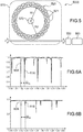
- FIGS. 7A and 7B schematically illustrate a first variant of a suspended arrangement of the micro-resonator according to the invention, respectively in a top view in a horizontal plane, and in a sectional view in a vertical plane.
- the micro-resonator 720 is arranged suspended above a substrate 772, resting on a pedestal 770.
- the pedestal 770 is centered on the geometric center of the micro-resonator 720.
- the pedestal 770 preferably has the shape of a cylinder, the base of which has a diameter D1 of between 0.25 and 0.75 times the average diameter D2 of the micro-resonator (average of the internal diameter and of the external diameter), preferably between 0.25 and 0.5 times this diameter D2.
- the pedestal is preferably, but not limited to, a cylinder of revolution. It may also be a cylinder with a non-circular base, for example with an oval base. The diameter D1 is then the greatest width of the base of the cylinder.
- the elementary waveguides 721 making up the micro-resonator are all mounted integral with the same support plate 771.
- the assembly consisting of the elementary waveguides 721 and of the support plate 771 can be formed by etching a single layer of material, so that there is physically no interface between a guide. wave element 721 and the support plate 771.
- the elementary waveguides are located on top of the support plate 771.
- the support plate 771 has a reduced thickness, at least three times less than the thickness of the elementary waveguides, or even at least ten times less, so that it does not influence the optical guidance in the micro-resonator .
- the elementary waveguides does not protrude outside a zone delimited by the elementary waveguides.
- it may have other shapes, for example a ring shape, suspended around the pedestal by means of internal arms.
- the figures 8A and 8B illustrate a second variant of a suspended arrangement of the micro-resonator according to the invention, respectively in a top view in a horizontal plane, and in a sectional view in a vertical plane.
- the elementary waveguides are kept suspended around the pedestal 870 by means of arms which extend parallel to the plane of the micro-resonator.
- the upper faces of the arms extend in a plane parallel to the plane of the micro-resonator.
- the arms here comprise so-called peripheral arms, 875, which each extend between an elementary waveguide 821 and the neighboring elementary waveguide, and so-called internal arms, 876, which each extend between an elementary waveguide. elemental wave 821 and the pedestal 870.
- the arms in particular the peripheral arms, 875, each have a width LB much less than that of the elementary waveguides, for example at least 3 times less, and even at least 4 times or 5 times less.
- all the elementary waveguides 821 are connected in pairs by peripheral arms 875, and four internal arms 876 extend crosswise and meet above the pedestal 870.
- the arms 875 and 876 are formed with the elementary waveguides in the same layer, and have the same thickness h 1 as the latter (see figure 8B ).
- FIGS. 9A to 9D illustrate different variants of a micro-resonator in a third embodiment of an optical device and an optical sensor according to the invention.
- the micro-resonator is arranged suspended above the pedestal, thanks to a support plate of the type described with reference to figures 7A and 7B .
- the support plate is crossed according to its thickness by trenches 925, or grooves, or slots.
- Each trench 925 extends from an outer edge of the support plate, to a central region of the plate, and passes between two neighboring elementary waveguides 921.
- the trenches each extend to the pedestal.
- each trench 925 passes through the support plate along its entire thickness, forming a through opening in said plate.
- Each trench 925 here extends along a radius of the ring micro-resonator.
- the support plate 971A comprises two trenches 925. These two trenches define laterally, on the support plate 971, a so-called isolated zone 9711A.
- the isolated area 9711A here receives a single elementary waveguide 921, called an isolated waveguide, the movement of which relative to the other elementary waveguides is released.
- the isolated waveguide can move horizontally in the plane of the micro-resonator 920A, according to a rotational movement about an axis parallel to (Oz).
- This increase in losses is detected by the analysis device, which can deduce therefrom an amplitude of the movement of the isolated waveguide.
- a micro-resonator is thus produced, and therefore an optical device and sensor according to the invention, sensitive to a greater variety of external stresses, in comparison with the prior art.
- the 920B micro-resonator of the figure 9B differs from that of the figure 9A that the isolated zone 9711B receives several neighboring elementary waveguides 921.
- the 920C micro-resonator of the figure 9C differs from that of the figure 9A that the support plate 971C comprises two isolated zones 9711C, each being delimited laterally by a pair of two trenches.
- Each isolated zone 9711C here receives a single elementary waveguide.
- the two pairs of trenches are here arranged symmetrical to one another, in planar symmetry relative to a plane orthogonal to the plane of the micro-resonator.
- the 920D micro-resonator of the figure 9D differs from that of the figure 9A that the support plate 971D has a plurality of trenches defining a plurality of isolated areas 9711D.
- the isolated areas 9711D are symmetrical in pairs, in planar symmetries relative to a respective plane, orthogonal to the plane of the micro-resonator 920D.
- Each isolated zone 9711D here receives several elementary waveguides.
- the distribution of the trenches makes it possible to favor one or the other movement of the elementary waveguides.
- n avg _ 1 designates the average refractive index of the core of the micro-resonator, in the operating mode.
- n ave _2 denotes the average refractive index of the core of the structure formed by the elementary waveguides remaining in the plane of the micro-resonator, in the extinction mode.
- ⁇ designates the wavelength of the light beam propagating in the micro-resonator in the operating mode, or resonance wavelength used.
- the operating mode corresponds to normal operating conditions as described above.
- the elementary waveguides remaining in the PH1 plane do not carry out any optical guidance of the signal arriving via the injection, respectively injection and extraction waveguide. In other words, they form an open switch. We notice that they indeed verify the condition of a Bragg mirror.
- the figures 10A and 10B illustrate two variants of a coupling zone of an injection and extraction waveguide according to the invention.
- Said coupling zone is located near the micro-resonator, where the evanescent coupling occurs between the injection and extraction waveguide and the micro-resonator. In order to promote this coupling, it is possible to improve the phase agreement between the respective modes propagated in the injection and extraction waveguide and in the micro-resonator.
- phase matching is respected when the respective effective indices of the injection and extraction waveguide and of the micro-resonator are identical.
- the width of the injection and extraction waveguide 1010A gradually decreases and then increases again, as one approaches, then moves away from the micro-resonator 1020.
- the injection and extraction waveguide 1010A then comprises a zone 10101 of reduced width, adjacent to the micro-resonator, two zones 10102 of adiabatic coupling (tapers), of decreasing width, respectively increasing, and two zones 10103 of greater width, on either side of zone 10101.
- the coupling can be favored using an injection and extraction waveguide 1010B, the shape of which gradually varies until it approaches the segmented shape of the micro-resonator (see figure 10B ).
- the injection and extraction waveguide 1010B is segmented, in a region adjacent to the micro-resonator.
- the transition from straight guide to segmented guide is made using a central zone 10104 (taper), solid, the width of which decreases as it approaches the micro-resonator.
- the shape of the injection and extraction waveguide 1010B is delimited by an outer envelope, the width of which increases as it approaches the micro-resonator.
- segments 10105 are distributed at a periodic pitch on either side of the central zone 10104.
- the segments 10105 each extend from the central zone 10104 to the envelope. external.
- the injection and extraction waveguide 1010B now only comprises segments 10105, which each extend from one edge to the other of the outer envelope.
- the distribution pitch of the segments 10105 is substantially equal to the distribution pitch of the elementary waveguides of the micro-resonator.
- micro-resonator coupled to a mechanical oscillator, or itself forming a mechanical oscillator.
- the micro-resonator is frozen, and an ancillary element moves in its near field, the ancillary element possibly being an injection and / or extraction waveguide.
- the elementary waveguides may not be arranged in a ring shape, but in another form of closed loop, for example a triangle with rounded angles, a rectangle with rounded angles, a so-called shape of a track. race (or " Racetrack ", in English, formed of two semicircles joined by two parallel segments), etc.
- the optical device according to the invention can also comprise a plurality of micro-resonators according to the invention, optically coupled to one another by an evanescent coupling.
- the optical sensor according to the invention makes it possible to detect and measure nanometric displacements (for example less than 20 nm), within the micro-resonator or in its near field.
- nanometric displacements can be generated by a stress such as an acceleration of the reference frame receiving the optical device according to the invention, a rotation of this reference frame, a displacement of a particle of non-zero mass (for example a particle falling on a nano -beam as described above), a photon displacement, an atom displacement, etc.
- a stress such as an acceleration of the reference frame receiving the optical device according to the invention, a rotation of this reference frame, a displacement of a particle of non-zero mass (for example a particle falling on a nano -beam as described above), a photon displacement, an atom displacement, etc.
- the analysis device can be arranged to convert the measurement of such displacement, into a value of acceleration, or angular velocity, or mass, or electromagnetic radiation, or atom displacement, etc., to thus forming a sensor of the accelerometer type, or gyrometer, or sensor sensitive to the mass such as a mass spectrometer, or radiation pressure sensor, or sensor for a source of photons, etc.
- the invention does not relate to the micro-resonator optical device as such.
- the figure 11 schematically illustrates an example of a method of manufacturing an optical device according to the invention.
- the device being manufactured is shown in a top view.
- the manufacturing process uses a so-called SOI (for “ Silicon On Insulator ”) stack, made up of the following three superimposed layers: a substrate 101 (for example in silicon), an intermediate layer 102 in silicon dioxide, and an upper layer 103 in silicon (starting point 11).
- SOI Silicon On Insulator
- the upper silicon layer 103 is etched over its entire thickness, here to form the injection and extraction waveguide 1110 and a notched silicon disc 104.
- Each notch of the notched disc 104 corresponds to an elementary waveguide 1121 of the micro-resonator.
- the method according to the invention then comprises a step 13 of etching the disc 104, over only part of its thickness. During this step 13, the disc 104 is etched in a central region thereof, to form the micro-resonator 1120.
- the etching retains a small thickness of the central region of the disc 104, which makes it possible to ensure the mechanical strength of the micro-resonator 1120, and in particular to keep the elementary waveguides 1121 integral with each other (cf. support plate described with reference to figures 7A and 7B ).
- step 12 a full disc is etched (and not a notched disc).
- step 13 the solid disc is etched over part of its thickness, in a central region and in annular regions thereof.
- the elementary waveguides are then placed on a residual disc of small thickness.
- the intermediate layer 102 is etched over its entire thickness to form a cavity 105 under the micro-resonator 1120 and the injection and extraction waveguide 1110.
- the etching preserves, under the micro-resonator 1120, a pedestal 1170 to hold the micro-resonator 1120 suspended above the substrate 101.
- the pedestal 1170 is approximately centered on the center of the micro-resonator 1120.
- the intermediate layer remaining around the cavity 105 serves in particular for the mechanical maintenance of the injection and extraction waveguide 1110, in suspension above the substrate 101.
- the engraving is here a wet etching in time.
- Each of the engravings preferably uses an engraving mask.
- An additional mobile element can, like the injection and extraction waveguide, be etched in the upper silicon layer 103.
- the additional mobile element may be made of a material different from that of the waveguides. It is for example a carbon nanotube.
Landscapes
- Physics & Mathematics (AREA)
- General Physics & Mathematics (AREA)
- Optics & Photonics (AREA)
- Engineering & Computer Science (AREA)
- Electromagnetism (AREA)
- Power Engineering (AREA)
- Radar, Positioning & Navigation (AREA)
- Remote Sensing (AREA)
- Investigating Or Analysing Materials By Optical Means (AREA)
- Optical Integrated Circuits (AREA)
Claims (15)
- Optischer Sensor (1000; 1000'; 5000), enthaltend:- eine optische Vorrichtung (100; 100'; 500) mit einem Wellenleiter-Mikroresonator (120; 520; 720; 820; 920A; 920B; 920C; 920D; 1020; 1120), der dazu vorgesehen ist, einen Lichtstrahl entlang eines geschlossenen optischen Pfades zu führen, und mit einem Einkopplungs- und Auskopplungswellenleiter (110; 1010A; 1010B; 1110) oder einem Einkopplungswellenleiter (110A) und einem Auskopplungswellenleiter (110B), die zur Einkopplung und Auskopplung des Lichtstrahls optisch mit dem Mikroresonator gekoppelt ist/sind;- einen Photodetektor (150; 550), der am Ausgang des Einkopplungs- und Auskopplungswellenleiters bzw. am Ausgang des Auskopplungswellenleiters angeordnet ist; und- eine Analysevorrichtung (160; 560), die am Eingang ein Signal empfängt, das von dem Photodetektor bereitgestellt wird, und die dazu vorgesehen ist, dieses Signal mit Bezugsdaten zu vergleichen und daraus eine Information über eine Verschiebung innerhalb der optischen Vorrichtung (100; 100'; 500) abzuleiten;wobei der Mikroresonator aus einer Mehrzahl von elementaren Wellenleitern (121; 521; 721; 821; 921; 1121) besteht, die voneinander beabstandet sind und in Schleifenanordnung nacheinander angeordnet sind.
- Optischer Sensor (1000; 1000') nach Anspruch 1,
dadurch gekennzeichnet, dass er ferner ein bewegliches Zusatzelement (130) enthält, das dazu ausgelegt ist, sich relativ zum Mikroresonator so zu verschieben, dass es einen Freiraum (122) zwischen zwei benachbarten, elementaren Wellenleitern teilweise oder vollständig durchquert. - Optischer Sensor (5000) nach Anspruch 1 oder 2,
dadurch gekennzeichnet, dass die elementaren Wellenleiter (521; 721; 821; 921; 1121) des Mikroresonators über einem Substrat (772; 872; 101) und um einen Sockel (570; 770; 870; 1170) herum aufgehängt sind. - Optischer Sensor (5000) nach Anspruch 3,
dadurch gekennzeichnet, dass der Sockel (570; 770; 870; 1170) eine Zylinderform aufweist, wobei die Grundfläche des Zylinders einen Durchmesser (D1) zwischen dem 0,25- und 0,75-fachen des Durchmessers (D2) des Mikroresonators liegt. - Optischer Sensor (5000) nach Anspruch 3 oder 4,
dadurch gekennzeichnet, dass die elementaren Wellenleiter (521; 721; 921; 1121) des Mikroresonators fest an einer Tragplatte (771; 971A; 971B; 971C; 971D) angebracht sind, die sich ihrerseits an dem Sockel abstützt. - Optischer Sensor (5000) nach Anspruch 5,
dadurch gekennzeichnet, dass die Tragplatte einen oder mehrere Gräben (925) aufweist, wobei jeder dieser Gräben sich von einem zwischen zwei benachbarten elementaren Wellenleitern liegenden Umfangsbereich der Tragplatte zu einem zentralen Bereich der Tragplatte erstreckt. - Optischer Sensor nach Anspruch 6,
dadurch gekennzeichnet, dass die Tragplatte zumindest ein Paar von Gräben (925) aufweist, wobei jedes Paar an der Tragplatte einen isolierten Bereich (9711A; 9711B; 9711C; 9711D) begrenzt, der einen oder mehrere elementare Wellenleiter aufnimmt. - Optischer Sensor nach Anspruch 7,
dadurch gekennzeichnet, dass die Tragplatte (971A; 971B) ein einzelnes Paar von Gräben aufweist. - Optischer Sensor nach Anspruch 7,
dadurch gekennzeichnet, dass die Tragplatte (971C) zwei Paare von Gräben aufweist, die symmetrisch zueinander angeordnet sind. - Optischer Sensor nach Anspruch 6,
dadurch gekennzeichnet, dass die Tragplatte (971D) eine Mehrzahl von Gräben aufweist, die zusammen eine Mehrzahl von isolierten Bereichen (9711D) begrenzen, die paarweise symmetrisch sind. - Optischer Sensor nach Anspruch 6,
dadurch gekennzeichnet, dass die Tragplatte eine Mehrzahl von Gräben (925) aufweist, die periodisch über die Tragplatte verteilt sind, so dass sie eine Mehrzahl von beweglichen, elementaren Wellenleitern isolieren, und dass der optische Sensor ferner Steuerungsmittel enthält, um die Verschiebung der beweglichen, elementaren Wellenleitern so zu steuern, dass sie wechselweise positioniert werden:- in der Ebene des Mikroresonators in einer Position, in welcher die elementaren Wellenleiter des Mikroresonators zusammen gemäß einem Verteilungsschritt (P) verteilt sind, der kleiner als - außerhalb der Ebene des Mikroresonators in einer Position, in welcher die in der Ebene des Mikroresonators verbleibenden elementaren Wellenleiter zusammen gemäß einem Verteilungsschritt verteilt sind, der gleich
- Optischer Sensor nach Anspruch 3 oder 4,
dadurch gekennzeichnet, dass die elementaren Wellenleiter (821) um den Sockel (870) herum über Arme (875, 876) aufgehängt sind, die sich in einer Ebene parallel zur Ebene des Mikroresonators erstrecken. - Optischer Sensor (1000; 1000') nach Anspruch 1 oder 2,
dadurch gekennzeichnet, dass die elementaren Wellenleiter (121) ohne Hebelarm in Abstützung an einem Substrat (172) liegen. - Optischer Sensor (1000; 1000'; 5000) nach einem der Ansprüche 1 bis 13,
dadurch gekennzeichnet, dass die elementaren Wellenleiter (121; 521; 721; 821; 921; 1121) des Mikroresonators periodisch nacheinander gemäß einem gleichmäßigen Schritt, Verteilungsschritt genannt, verteilt sind. - Optischer Sensor nach Anspruch 14,
dadurch gekennzeichnet, dass der Verteilungsschritt (P) kleiner ist als worin λ eine Resonanzwellenlänge des Mikroresonators ist; undnh der mittlere Brechungsindex der elementaren Wellenleiter ist.
Applications Claiming Priority (1)
| Application Number | Priority Date | Filing Date | Title |
|---|---|---|---|
| FR1756293A FR3068778B1 (fr) | 2017-07-04 | 2017-07-04 | Capteur de deplacement avec micro-resonateur en anneau segmente. |
Publications (2)
| Publication Number | Publication Date |
|---|---|
| EP3425344A1 EP3425344A1 (de) | 2019-01-09 |
| EP3425344B1 true EP3425344B1 (de) | 2021-03-24 |
Family
ID=60515461
Family Applications (1)
| Application Number | Title | Priority Date | Filing Date |
|---|---|---|---|
| EP18181241.3A Active EP3425344B1 (de) | 2017-07-04 | 2018-07-02 | Bewegungssensor mit mikroresonator mit segmentiertem ring |
Country Status (3)
| Country | Link |
|---|---|
| US (1) | US10578437B2 (de) |
| EP (1) | EP3425344B1 (de) |
| FR (1) | FR3068778B1 (de) |
Families Citing this family (10)
| Publication number | Priority date | Publication date | Assignee | Title |
|---|---|---|---|---|
| FR3056306B1 (fr) | 2016-09-20 | 2019-11-22 | Commissariat A L'energie Atomique Et Aux Energies Alternatives | Guide optique presentant un virage a pseudo-gradient d'indice |
| FR3069707B1 (fr) | 2017-07-27 | 2019-08-30 | Commissariat A L'energie Atomique Et Aux Energies Alternatives | Dispositif infrarouge |
| FR3074587B1 (fr) | 2017-12-06 | 2020-01-03 | Commissariat A L'energie Atomique Et Aux Energies Alternatives | Puce photonique a repliement de trajet optique et structure de collimation integree |
| FR3077652B1 (fr) | 2018-02-05 | 2022-05-27 | Commissariat Energie Atomique | Puce photonique a structure de collimation integree |
| FR3078155B1 (fr) | 2018-02-19 | 2020-08-14 | Commissariat Energie Atomique | Capteur photo-acoustique avec couplage opto-mecanique. |
| FR3087904B1 (fr) | 2018-10-26 | 2020-11-13 | Commissariat Energie Atomique | Resonateur opto-mecanique a guide d'onde sub-longueur d'onde |
| US11566900B2 (en) * | 2019-03-06 | 2023-01-31 | Purdue Research Foundation | MEMS rotation rate sensor |
| FR3112402B1 (fr) | 2020-07-07 | 2022-10-28 | Commissariat Energie Atomique | Dispositif de démultiplexage en longueur d’onde notamment pour un démultiplexage hors plan. |
| FR3143141B1 (fr) * | 2022-12-08 | 2024-10-25 | Commissariat Energie Atomique | Dispositif photonique isolé mécaniquement d'un substrat |
| IT202300016515A1 (it) * | 2023-08-03 | 2025-02-03 | Qopsys S R L | Struttura di motore a risonanza fotonica planare |
Family Cites Families (8)
| Publication number | Priority date | Publication date | Assignee | Title |
|---|---|---|---|---|
| US55202A (en) * | 1866-05-29 | Improvement in sawing-machines | ||
| US6665476B2 (en) * | 2000-09-29 | 2003-12-16 | Sarnoff Corporation | Wavelength selective optical add/drop multiplexer and method of manufacture |
| US8195011B2 (en) * | 2008-03-03 | 2012-06-05 | Ramot At Tel-Aviv University Ltd. | Electro-optical modulator structure |
| GB201209837D0 (en) * | 2012-06-01 | 2012-08-29 | Univ Bristol | Orbital angular momentum |
| EP2917691B1 (de) * | 2013-04-02 | 2020-06-03 | Politecnico di Bari | Optischer drehsensor sowie verfahren zur herstellung eines optischen drehsensors |
| US9239340B2 (en) * | 2013-12-13 | 2016-01-19 | Intel Corporation | Optomechanical sensor for accelerometry and gyroscopy |
| US10215918B2 (en) * | 2015-11-24 | 2019-02-26 | Omega Optics, Inc. | Subwavelength photonic crystal waveguide in optical systems |
| FR3054664B1 (fr) | 2016-07-27 | 2018-09-07 | Commissariat A L'energie Atomique Et Aux Energies Alternatives | Dispositif optique a micro-resonateur en anneau segmente pour un capteur biologique ou chimique |
-
2017
- 2017-07-04 FR FR1756293A patent/FR3068778B1/fr not_active Expired - Fee Related
-
2018
- 2018-07-02 EP EP18181241.3A patent/EP3425344B1/de active Active
- 2018-07-03 US US16/026,535 patent/US10578437B2/en active Active
Non-Patent Citations (1)
| Title |
|---|
| None * |
Also Published As
| Publication number | Publication date |
|---|---|
| FR3068778B1 (fr) | 2019-08-30 |
| US20190011261A1 (en) | 2019-01-10 |
| US10578437B2 (en) | 2020-03-03 |
| FR3068778A1 (fr) | 2019-01-11 |
| EP3425344A1 (de) | 2019-01-09 |
Similar Documents
| Publication | Publication Date | Title |
|---|---|---|
| EP3425344B1 (de) | Bewegungssensor mit mikroresonator mit segmentiertem ring | |
| EP3276337B1 (de) | Optische vorrichtung mit mikroresonator mit segmentiertem ring | |
| EP3460547B1 (de) | Optische kopplungsvorrichtung für einen photonenschaltkreis | |
| EP3147673B1 (de) | Optomechanischer physikalischer sensor mit verbesserter empfindlichkeit | |
| EP2930506B1 (de) | Erkennungsvorrichtung mit akustischem resonator für differentialanwendungen vom typ helmholtz-resonator | |
| EP3385784A1 (de) | Optoelektronische vorrichtung zur erzeugung eines frequenzkamms | |
| EP3494381B1 (de) | Absorptionskavität mit eingangs- und ausgangswellenleitern für einen biologischen oder chemischen sensor | |
| EP3147646A1 (de) | Bildgebende vorrichtung ohne linse und damit verbundenes beobachtungsverfahren | |
| WO2018138223A1 (fr) | Détecteur optique de particules | |
| EP4016054B1 (de) | Optische komponente für eine atr-bildgebungsvorrichtung | |
| EP3447549A1 (de) | Halbleiterstruktur mit gespannt aufgehängter membran, die einen optischen hohlraum enthält | |
| EP3647738B1 (de) | Optomechanischer resonator mit wellenleiter mit subwellenlänge | |
| WO2009127794A1 (fr) | Spectrometre compact a echantillonage bidimensionnel | |
| EP4009456A1 (de) | Verfahren zur herstellung eines verteilten bragg-spiegels | |
| WO2017220919A1 (fr) | Reflecteur optique resonant a multiples couches minces de materiaux dielectriques, capteur optique, dispositif d'amplification laser comportant un tel reflecteur et procedes de fabrication correspondants | |
| EP3486603A1 (de) | System zur umwandlung einer bewegung in eine optische phasenverschiebung | |
| FR2739195A1 (fr) | Coupleur optique a bande etroite utilisant l'excitation des modes de galerie d'un element resonateur dielectrique de forme de revolution | |
| EP3968066A1 (de) | Wellenleiter, der eine optische multimode-faser umfasst und die geführten moden räumlich konzentrieren kann | |
| EP4034923B1 (de) | Optisches system und verfahren zu dessen herstellung | |
| FR3023414A1 (fr) | Detecteur propre a detecter une premiere longueur d'onde et a filtrer une deuxieme longueur d'onde | |
| EP3936912A1 (de) | Wellenlängen-demultiplexervorrichtung, insbesondere für out-of-plane-demultiplexing | |
| EP0542603A1 (de) | Faseroptischer Sensor zur Erfassung eines Parameters, Verfahren zum Auswerten eines solchen Parameters, und Verwendung des Sensors zur Gasmessung | |
| FR3154806A1 (fr) | Système opto-mécanique de transduction pour la spectrométrie photo-acoustique | |
| EP4657679A1 (de) | Quantenkaskadenlaser im mittleren infrarotbereich | |
| FR3143112A1 (fr) | Dispositif de mesure d’une grandeur physique utilisant l’effet Vernier optique |
Legal Events
| Date | Code | Title | Description |
|---|---|---|---|
| PUAI | Public reference made under article 153(3) epc to a published international application that has entered the european phase |
Free format text: ORIGINAL CODE: 0009012 |
|
| STAA | Information on the status of an ep patent application or granted ep patent |
Free format text: STATUS: REQUEST FOR EXAMINATION WAS MADE |
|
| 17P | Request for examination filed |
Effective date: 20180702 |
|
| AK | Designated contracting states |
Kind code of ref document: A1 Designated state(s): AL AT BE BG CH CY CZ DE DK EE ES FI FR GB GR HR HU IE IS IT LI LT LU LV MC MK MT NL NO PL PT RO RS SE SI SK SM TR |
|
| AX | Request for extension of the european patent |
Extension state: BA ME |
|
| GRAP | Despatch of communication of intention to grant a patent |
Free format text: ORIGINAL CODE: EPIDOSNIGR1 |
|
| STAA | Information on the status of an ep patent application or granted ep patent |
Free format text: STATUS: GRANT OF PATENT IS INTENDED |
|
| INTG | Intention to grant announced |
Effective date: 20201103 |
|
| GRAS | Grant fee paid |
Free format text: ORIGINAL CODE: EPIDOSNIGR3 |
|
| GRAA | (expected) grant |
Free format text: ORIGINAL CODE: 0009210 |
|
| STAA | Information on the status of an ep patent application or granted ep patent |
Free format text: STATUS: THE PATENT HAS BEEN GRANTED |
|
| AK | Designated contracting states |
Kind code of ref document: B1 Designated state(s): AL AT BE BG CH CY CZ DE DK EE ES FI FR GB GR HR HU IE IS IT LI LT LU LV MC MK MT NL NO PL PT RO RS SE SI SK SM TR |
|
| REG | Reference to a national code |
Ref country code: GB Ref legal event code: FG4D Free format text: NOT ENGLISH |
|
| REG | Reference to a national code |
Ref country code: CH Ref legal event code: EP |
|
| REG | Reference to a national code |
Ref country code: DE Ref legal event code: R096 Ref document number: 602018014259 Country of ref document: DE |
|
| REG | Reference to a national code |
Ref country code: IE Ref legal event code: FG4D Free format text: LANGUAGE OF EP DOCUMENT: FRENCH |
|
| REG | Reference to a national code |
Ref country code: AT Ref legal event code: REF Ref document number: 1374946 Country of ref document: AT Kind code of ref document: T Effective date: 20210415 |
|
| REG | Reference to a national code |
Ref country code: LT Ref legal event code: MG9D |
|
| PG25 | Lapsed in a contracting state [announced via postgrant information from national office to epo] |
Ref country code: NO Free format text: LAPSE BECAUSE OF FAILURE TO SUBMIT A TRANSLATION OF THE DESCRIPTION OR TO PAY THE FEE WITHIN THE PRESCRIBED TIME-LIMIT Effective date: 20210624 Ref country code: HR Free format text: LAPSE BECAUSE OF FAILURE TO SUBMIT A TRANSLATION OF THE DESCRIPTION OR TO PAY THE FEE WITHIN THE PRESCRIBED TIME-LIMIT Effective date: 20210324 Ref country code: FI Free format text: LAPSE BECAUSE OF FAILURE TO SUBMIT A TRANSLATION OF THE DESCRIPTION OR TO PAY THE FEE WITHIN THE PRESCRIBED TIME-LIMIT Effective date: 20210324 Ref country code: GR Free format text: LAPSE BECAUSE OF FAILURE TO SUBMIT A TRANSLATION OF THE DESCRIPTION OR TO PAY THE FEE WITHIN THE PRESCRIBED TIME-LIMIT Effective date: 20210625 Ref country code: BG Free format text: LAPSE BECAUSE OF FAILURE TO SUBMIT A TRANSLATION OF THE DESCRIPTION OR TO PAY THE FEE WITHIN THE PRESCRIBED TIME-LIMIT Effective date: 20210624 |
|
| PG25 | Lapsed in a contracting state [announced via postgrant information from national office to epo] |
Ref country code: RS Free format text: LAPSE BECAUSE OF FAILURE TO SUBMIT A TRANSLATION OF THE DESCRIPTION OR TO PAY THE FEE WITHIN THE PRESCRIBED TIME-LIMIT Effective date: 20210324 Ref country code: LV Free format text: LAPSE BECAUSE OF FAILURE TO SUBMIT A TRANSLATION OF THE DESCRIPTION OR TO PAY THE FEE WITHIN THE PRESCRIBED TIME-LIMIT Effective date: 20210324 Ref country code: SE Free format text: LAPSE BECAUSE OF FAILURE TO SUBMIT A TRANSLATION OF THE DESCRIPTION OR TO PAY THE FEE WITHIN THE PRESCRIBED TIME-LIMIT Effective date: 20210324 |
|
| REG | Reference to a national code |
Ref country code: NL Ref legal event code: MP Effective date: 20210324 |
|
| REG | Reference to a national code |
Ref country code: AT Ref legal event code: MK05 Ref document number: 1374946 Country of ref document: AT Kind code of ref document: T Effective date: 20210324 |
|
| PG25 | Lapsed in a contracting state [announced via postgrant information from national office to epo] |
Ref country code: NL Free format text: LAPSE BECAUSE OF FAILURE TO SUBMIT A TRANSLATION OF THE DESCRIPTION OR TO PAY THE FEE WITHIN THE PRESCRIBED TIME-LIMIT Effective date: 20210324 |
|
| PG25 | Lapsed in a contracting state [announced via postgrant information from national office to epo] |
Ref country code: LT Free format text: LAPSE BECAUSE OF FAILURE TO SUBMIT A TRANSLATION OF THE DESCRIPTION OR TO PAY THE FEE WITHIN THE PRESCRIBED TIME-LIMIT Effective date: 20210324 Ref country code: CZ Free format text: LAPSE BECAUSE OF FAILURE TO SUBMIT A TRANSLATION OF THE DESCRIPTION OR TO PAY THE FEE WITHIN THE PRESCRIBED TIME-LIMIT Effective date: 20210324 Ref country code: EE Free format text: LAPSE BECAUSE OF FAILURE TO SUBMIT A TRANSLATION OF THE DESCRIPTION OR TO PAY THE FEE WITHIN THE PRESCRIBED TIME-LIMIT Effective date: 20210324 Ref country code: SM Free format text: LAPSE BECAUSE OF FAILURE TO SUBMIT A TRANSLATION OF THE DESCRIPTION OR TO PAY THE FEE WITHIN THE PRESCRIBED TIME-LIMIT Effective date: 20210324 Ref country code: AT Free format text: LAPSE BECAUSE OF FAILURE TO SUBMIT A TRANSLATION OF THE DESCRIPTION OR TO PAY THE FEE WITHIN THE PRESCRIBED TIME-LIMIT Effective date: 20210324 |
|
| PG25 | Lapsed in a contracting state [announced via postgrant information from national office to epo] |
Ref country code: IS Free format text: LAPSE BECAUSE OF FAILURE TO SUBMIT A TRANSLATION OF THE DESCRIPTION OR TO PAY THE FEE WITHIN THE PRESCRIBED TIME-LIMIT Effective date: 20210724 Ref country code: SK Free format text: LAPSE BECAUSE OF FAILURE TO SUBMIT A TRANSLATION OF THE DESCRIPTION OR TO PAY THE FEE WITHIN THE PRESCRIBED TIME-LIMIT Effective date: 20210324 Ref country code: RO Free format text: LAPSE BECAUSE OF FAILURE TO SUBMIT A TRANSLATION OF THE DESCRIPTION OR TO PAY THE FEE WITHIN THE PRESCRIBED TIME-LIMIT Effective date: 20210324 Ref country code: PT Free format text: LAPSE BECAUSE OF FAILURE TO SUBMIT A TRANSLATION OF THE DESCRIPTION OR TO PAY THE FEE WITHIN THE PRESCRIBED TIME-LIMIT Effective date: 20210726 Ref country code: PL Free format text: LAPSE BECAUSE OF FAILURE TO SUBMIT A TRANSLATION OF THE DESCRIPTION OR TO PAY THE FEE WITHIN THE PRESCRIBED TIME-LIMIT Effective date: 20210324 |
|
| REG | Reference to a national code |
Ref country code: DE Ref legal event code: R097 Ref document number: 602018014259 Country of ref document: DE |
|
| PG25 | Lapsed in a contracting state [announced via postgrant information from national office to epo] |
Ref country code: ES Free format text: LAPSE BECAUSE OF FAILURE TO SUBMIT A TRANSLATION OF THE DESCRIPTION OR TO PAY THE FEE WITHIN THE PRESCRIBED TIME-LIMIT Effective date: 20210324 Ref country code: DK Free format text: LAPSE BECAUSE OF FAILURE TO SUBMIT A TRANSLATION OF THE DESCRIPTION OR TO PAY THE FEE WITHIN THE PRESCRIBED TIME-LIMIT Effective date: 20210324 Ref country code: AL Free format text: LAPSE BECAUSE OF FAILURE TO SUBMIT A TRANSLATION OF THE DESCRIPTION OR TO PAY THE FEE WITHIN THE PRESCRIBED TIME-LIMIT Effective date: 20210324 |
|
| PLBE | No opposition filed within time limit |
Free format text: ORIGINAL CODE: 0009261 |
|
| STAA | Information on the status of an ep patent application or granted ep patent |
Free format text: STATUS: NO OPPOSITION FILED WITHIN TIME LIMIT |
|
| PG25 | Lapsed in a contracting state [announced via postgrant information from national office to epo] |
Ref country code: SI Free format text: LAPSE BECAUSE OF FAILURE TO SUBMIT A TRANSLATION OF THE DESCRIPTION OR TO PAY THE FEE WITHIN THE PRESCRIBED TIME-LIMIT Effective date: 20210324 |
|
| REG | Reference to a national code |
Ref country code: CH Ref legal event code: PL |
|
| 26N | No opposition filed |
Effective date: 20220104 |
|
| PG25 | Lapsed in a contracting state [announced via postgrant information from national office to epo] |
Ref country code: MC Free format text: LAPSE BECAUSE OF FAILURE TO SUBMIT A TRANSLATION OF THE DESCRIPTION OR TO PAY THE FEE WITHIN THE PRESCRIBED TIME-LIMIT Effective date: 20210324 |
|
| REG | Reference to a national code |
Ref country code: BE Ref legal event code: MM Effective date: 20210731 |
|
| PG25 | Lapsed in a contracting state [announced via postgrant information from national office to epo] |
Ref country code: LI Free format text: LAPSE BECAUSE OF NON-PAYMENT OF DUE FEES Effective date: 20210731 Ref country code: CH Free format text: LAPSE BECAUSE OF NON-PAYMENT OF DUE FEES Effective date: 20210731 |
|
| PG25 | Lapsed in a contracting state [announced via postgrant information from national office to epo] |
Ref country code: IS Free format text: LAPSE BECAUSE OF FAILURE TO SUBMIT A TRANSLATION OF THE DESCRIPTION OR TO PAY THE FEE WITHIN THE PRESCRIBED TIME-LIMIT Effective date: 20210724 Ref country code: LU Free format text: LAPSE BECAUSE OF NON-PAYMENT OF DUE FEES Effective date: 20210702 |
|
| PG25 | Lapsed in a contracting state [announced via postgrant information from national office to epo] |
Ref country code: IE Free format text: LAPSE BECAUSE OF NON-PAYMENT OF DUE FEES Effective date: 20210702 Ref country code: BE Free format text: LAPSE BECAUSE OF NON-PAYMENT OF DUE FEES Effective date: 20210731 |
|
| PG25 | Lapsed in a contracting state [announced via postgrant information from national office to epo] |
Ref country code: IT Free format text: LAPSE BECAUSE OF FAILURE TO SUBMIT A TRANSLATION OF THE DESCRIPTION OR TO PAY THE FEE WITHIN THE PRESCRIBED TIME-LIMIT Effective date: 20210324 |
|
| PG25 | Lapsed in a contracting state [announced via postgrant information from national office to epo] |
Ref country code: CY Free format text: LAPSE BECAUSE OF FAILURE TO SUBMIT A TRANSLATION OF THE DESCRIPTION OR TO PAY THE FEE WITHIN THE PRESCRIBED TIME-LIMIT Effective date: 20210324 |
|
| PG25 | Lapsed in a contracting state [announced via postgrant information from national office to epo] |
Ref country code: HU Free format text: LAPSE BECAUSE OF FAILURE TO SUBMIT A TRANSLATION OF THE DESCRIPTION OR TO PAY THE FEE WITHIN THE PRESCRIBED TIME-LIMIT; INVALID AB INITIO Effective date: 20180702 |
|
| PG25 | Lapsed in a contracting state [announced via postgrant information from national office to epo] |
Ref country code: MK Free format text: LAPSE BECAUSE OF FAILURE TO SUBMIT A TRANSLATION OF THE DESCRIPTION OR TO PAY THE FEE WITHIN THE PRESCRIBED TIME-LIMIT Effective date: 20210324 |
|
| PG25 | Lapsed in a contracting state [announced via postgrant information from national office to epo] |
Ref country code: TR Free format text: LAPSE BECAUSE OF FAILURE TO SUBMIT A TRANSLATION OF THE DESCRIPTION OR TO PAY THE FEE WITHIN THE PRESCRIBED TIME-LIMIT Effective date: 20210324 |
|
| PG25 | Lapsed in a contracting state [announced via postgrant information from national office to epo] |
Ref country code: MT Free format text: LAPSE BECAUSE OF FAILURE TO SUBMIT A TRANSLATION OF THE DESCRIPTION OR TO PAY THE FEE WITHIN THE PRESCRIBED TIME-LIMIT Effective date: 20210324 |
|
| PGFP | Annual fee paid to national office [announced via postgrant information from national office to epo] |
Ref country code: DE Payment date: 20250722 Year of fee payment: 8 |
|
| PGFP | Annual fee paid to national office [announced via postgrant information from national office to epo] |
Ref country code: GB Payment date: 20250724 Year of fee payment: 8 |
|
| PGFP | Annual fee paid to national office [announced via postgrant information from national office to epo] |
Ref country code: FR Payment date: 20250722 Year of fee payment: 8 |