EP3392778A1 - Dispositif de communication, procédé de communication, programme, et système de communication - Google Patents
Dispositif de communication, procédé de communication, programme, et système de communication Download PDFInfo
- Publication number
- EP3392778A1 EP3392778A1 EP16875423.2A EP16875423A EP3392778A1 EP 3392778 A1 EP3392778 A1 EP 3392778A1 EP 16875423 A EP16875423 A EP 16875423A EP 3392778 A1 EP3392778 A1 EP 3392778A1
- Authority
- EP
- European Patent Office
- Prior art keywords
- data
- word
- communication apparatus
- notification information
- sent
- Prior art date
- Legal status (The legal status is an assumption and is not a legal conclusion. Google has not performed a legal analysis and makes no representation as to the accuracy of the status listed.)
- Withdrawn
Links
Images



Classifications
-
- G—PHYSICS
- G06—COMPUTING OR CALCULATING; COUNTING
- G06F—ELECTRIC DIGITAL DATA PROCESSING
- G06F13/00—Interconnection of, or transfer of information or other signals between, memories, input/output devices or central processing units
- G06F13/38—Information transfer, e.g. on bus
- G06F13/42—Bus transfer protocol, e.g. handshake; Synchronisation
- G06F13/4282—Bus transfer protocol, e.g. handshake; Synchronisation on a serial bus, e.g. I2C bus, SPI bus
- G06F13/4291—Bus transfer protocol, e.g. handshake; Synchronisation on a serial bus, e.g. I2C bus, SPI bus using a clocked protocol
-
- G—PHYSICS
- G06—COMPUTING OR CALCULATING; COUNTING
- G06F—ELECTRIC DIGITAL DATA PROCESSING
- G06F11/00—Error detection; Error correction; Monitoring
- G06F11/07—Responding to the occurrence of a fault, e.g. fault tolerance
- G06F11/0703—Error or fault processing not based on redundancy, i.e. by taking additional measures to deal with the error or fault not making use of redundancy in operation, in hardware, or in data representation
- G06F11/0751—Error or fault detection not based on redundancy
- G06F11/0754—Error or fault detection not based on redundancy by exceeding limits
- G06F11/076—Error or fault detection not based on redundancy by exceeding limits by exceeding a count or rate limit, e.g. word- or bit count limit
-
- G—PHYSICS
- G06—COMPUTING OR CALCULATING; COUNTING
- G06F—ELECTRIC DIGITAL DATA PROCESSING
- G06F11/00—Error detection; Error correction; Monitoring
- G06F11/07—Responding to the occurrence of a fault, e.g. fault tolerance
- G06F11/08—Error detection or correction by redundancy in data representation, e.g. by using checking codes
- G06F11/10—Adding special bits or symbols to the coded information, e.g. parity check, casting out 9's or 11's
- G06F11/1004—Adding special bits or symbols to the coded information, e.g. parity check, casting out 9's or 11's to protect a block of data words, e.g. CRC or checksum
-
- G—PHYSICS
- G06—COMPUTING OR CALCULATING; COUNTING
- G06F—ELECTRIC DIGITAL DATA PROCESSING
- G06F13/00—Interconnection of, or transfer of information or other signals between, memories, input/output devices or central processing units
- G06F13/38—Information transfer, e.g. on bus
- G06F13/42—Bus transfer protocol, e.g. handshake; Synchronisation
- G06F13/4204—Bus transfer protocol, e.g. handshake; Synchronisation on a parallel bus
- G06F13/4221—Bus transfer protocol, e.g. handshake; Synchronisation on a parallel bus being an input/output bus, e.g. ISA bus, EISA bus, PCI bus, SCSI bus
- G06F13/423—Bus transfer protocol, e.g. handshake; Synchronisation on a parallel bus being an input/output bus, e.g. ISA bus, EISA bus, PCI bus, SCSI bus with synchronous protocol
-
- H—ELECTRICITY
- H04—ELECTRIC COMMUNICATION TECHNIQUE
- H04L—TRANSMISSION OF DIGITAL INFORMATION, e.g. TELEGRAPHIC COMMUNICATION
- H04L1/00—Arrangements for detecting or preventing errors in the information received
- H04L1/004—Arrangements for detecting or preventing errors in the information received by using forward error control
- H04L1/0056—Systems characterized by the type of code used
- H04L1/0061—Error detection codes
- H04L1/0063—Single parity check
-
- H—ELECTRICITY
- H04—ELECTRIC COMMUNICATION TECHNIQUE
- H04L—TRANSMISSION OF DIGITAL INFORMATION, e.g. TELEGRAPHIC COMMUNICATION
- H04L1/00—Arrangements for detecting or preventing errors in the information received
- H04L1/0078—Avoidance of errors by organising the transmitted data in a format specifically designed to deal with errors, e.g. location
- H04L1/0083—Formatting with frames or packets; Protocol or part of protocol for error control
-
- H—ELECTRICITY
- H04—ELECTRIC COMMUNICATION TECHNIQUE
- H04L—TRANSMISSION OF DIGITAL INFORMATION, e.g. TELEGRAPHIC COMMUNICATION
- H04L12/00—Data switching networks
- H04L12/28—Data switching networks characterised by path configuration, e.g. LAN [Local Area Networks] or WAN [Wide Area Networks]
- H04L12/40—Bus networks
- H04L12/4013—Management of data rate on the bus
-
- H—ELECTRICITY
- H04—ELECTRIC COMMUNICATION TECHNIQUE
- H04L—TRANSMISSION OF DIGITAL INFORMATION, e.g. TELEGRAPHIC COMMUNICATION
- H04L9/00—Cryptographic mechanisms or cryptographic arrangements for secret or secure communications; Network security protocols
- H04L9/40—Network security protocols
Definitions
- This communication apparatus includes a sending section configured to send data including a predetermined byte count per one word to another communication apparatus on a word basis in which the data is included and a confirmation section configured to confirm the data to be sent to the another communication apparatus so as to include notification information necessary for recognizing presence or absence of a word having invalid data into a signal to be transferred to the another communication apparatus.
- a communication method or a program includes the steps of sending data including a predetermined byte count per one word to another communication apparatus on a word basis in which the data is included and confirming the data to be sent to the another communication apparatus so as to include notification information necessary for recognizing presence or absence of a word having invalid data into a signal to be transferred to the another communication apparatus.
- the send/receive block 21 transfers signals by changing the potentials of the data signal line 14-1 and the clock signal line 14-2 between H level and the L level, thereby sending and receiving data and commands between the slaves 13-1 through 13-3. For example, when write data to be written to the slaves 13-1 through 13-3 is supplied from upper equipment not depicted, the send/receive block 21 sends the supplied write data to the slaves 13-1 through 13-3 on the basis of the word unit in which two-byte data is included per one word. In addition, when the read data read from the slaves 13-1 through 13-3 comes, the send/receive block 21 receives this read data and supplies the received read data to the upper equipment.
- the master 12 In the data send/receive operation in the bus IF 11 configured as described above, the master 12 always has the privilege of communication in which signals are transferred along the data signal line 14-1 with reference to the clock supplied by the master 12 to the clock signal line 14-2.
- the communication compliant with the standard of I3C is executed and, in the HDR mode of I3C, the three modes, the DDR (Double Data Rate) mode, the TSP (Ternary Symbol Pure-Bus) mode, and the TSL (Ternary Symbol Legacy-inclusive-Bus) mode, are defined by the standard.
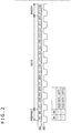
- the following describes a method of the notification of the presence or absence of a word having invalid data in each the DDR mode, the TSP mode, and the TSL mode with reference to FIG. 2 through FIG. 7 .
- a method of including notification information in the preamble can be used.
- preamble PR1 is “1” and preamble PR0 is “0,” notification information be indicative that the byte count of the valid data of the subsequent write data per one word is one byte. Further, it is assumed that, if preamble PR1 is "1” and preamble PR0 is "1,” notification information be indicative that the byte count of the valid data of the subsequent write data per one word is two bytes.
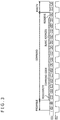
- a 1-word command is configured by a command code of eight bits D8 through D15, a slave address of seven bits D1 through D7, and a reserve of one bit D0. Further, of the command codes D8 through D15, command code D15 is a flag indicative of read/write.
- the master 12 can include the data length of the valid data of the entire write data or odd/even-number information of the valid data of the entire write data into a signal as the notification information necessary for the recognition of presence/absence of a word having invalid data.
- the slave 13 can recognize that there is a word having invalid data.
- the slave 13 can recognize that there is no word having invalid data.
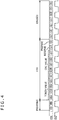
- CRC is configured by a token value of four bits D12 through D15, a CRC value of five bits D7 through D11, a reserve of one bit D6, a prepare of one bit D5, and an unused part of seven bits D0 through D4, P0, and P1.
- the recognition block 32 recognizes that there is a word having invalid data and the entire write data is odd-numbered, the word to be sent last becomes one byte, causing the send/receive block 31 to mask the invalid data of this last word.
- the configuration itself of CRC as illustrated in FIG. 4 may be changed so as to pad the byte count of the valid data of the entire write data as notification information, thereby transmitting the byte count of the entire write data along with a CRC value. It is also practicable to build the data length of the valid data of the entire write data into any one of the token value D12 through D15, the reserve D6, the prepare D5, and unused part D0 through D4, P0, and P1 or by use of a combination of one or more of these items.
- communication following the coding as illustrated in B of FIG. 5 can be executed by use of three state changes of the data signal line 14-1 and the clock signal line 14-2 as illustrated in A of FIG. 5 . That is, in the TSP mode or the TSL mode, three state changes of only the data signal line 14-1, only the clock signal line 14-2, or both the data signal line 14-1 and the clock signal line 14-2 are used. Consequently, the information of three-bits per two symbols can be transmitted.
- one word at the time of write transfer is configured by 18 bits for 12 symbols (a command or data of 16 bits and a parity of two bits).
- the master 12 can indicate whether the byte count of the valid data per one work is one byte or two bytes, thereby including the notification information necessary for the recognition of presence or absence of a word having invalid data into a signal. That is, sending write data on a one-word basis with data of two bytes per one word included allows the slave 13 to recognize that this word has invalid data if the notification information is indicative of one byte. On the other hand, if the notification information is indicative of two bytes, the slave 13 can recognize that this word does not have invalid data.
- the slave 13 can obtain the byte count of the valid data of the write data.
- the 12 symbols (six pairs) to be sent at normal time are illustrated in A of FIG. 7 and the special symbol pair (2, 2) is not used as illustrated. Therefore, in this case, the slave 13 can recognize that the byte count of the valid data of the write data per one word is two bytes.
- notification information can be included in a command as with the DDR mode described above.
- the configuration of a 1-word command is similar to that illustrated in FIG. 3 described above.
- the data length of the valid data of the entire write data can be padded in command codes D8 through D15 as notification information.
- the odd/even-number information (the information indicative of an even number or an odd number) of the valid data of the entire write data can be padded in command codes D8 through D15 as notification information.
- the odd/even-number information of the valid data of the entire write data can be padded in reserve D0 as notification information. It should be noted that, in the second example and the third example, the data length is not limited, so that these examples are suitably employed.
- the slave 13 sends read data to the master 12
- the presence or absence of the special symbol pair (2, 2) can be used; for example, the byte count of the valid data per one word of write data can be included in a signal as notification information. Consequently, the master 12 can confirm the signal for use by the slave 13 in sending data and recognize the presence or absence of invalid data on the basis of the notification information, thereby avoiding the execution of the processing based on invalid data.
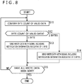
- FIG. 8 depicts a flowchart indicative of one example of the processing of sending write data by the master 12 illustrated in FIG. 1 . It should be noted that, as described with reference to FIG. 2 , the following describes a method of sending the information about the byte count of the valid data of the subsequent write data per one word by use of the preamble.
- the processing starts when the data to be written to the slave 13 is supplied from upper equipment not depicted to the master 12.
- step S11 the send/receive block 21 forms the sequentially supplied write data into a word-basis format and the confirmation block 22 confirms the byte count of the valid data of this write data per one word.
- step S12 the confirmation block 22 determines, as a result of the confirmation done in step S11, whether the byte count of the valid data of the write data per one word is one byte or two bytes.
- step S12 If the confirmation block 22 determines that the byte count of the valid data of the write data per one word is one byte in step S12, then the processing goes to step S13.
- step S13 the confirmation block 22 instructs the send/receive block 21 to include the notification information indicative that the byte count of the valid data of the write data per one word is one word into a signal. Accordingly, the send/receive block 21 sends, to the slave 13, the write data of one word with preamble PR1 of one word to be sent set to "1" and preamble PR0 to "0" as illustrated in FIG. 2 described above.
- step S12 determines that the byte count of the valid data of the write data per one word is two bytes in step S12, then the processing goes to step S14.
- step S14 the confirmation block 22 instructs the send/receive block 21 to include the notification information indicative that the byte count of the valid data of the write data per one word is two bytes into a signal. Accordingly, the send/receive block 21 sends, to the slave 13, the write data of one word with preamble PR1 of one word to be sent set to "1" and preamble PR0 to "1" as illustrated in FIG. 2 described above.
- step S13 or S14 After the completion of the processing of step S13 or S14, the processing goes to step S15 in which the send/receive block 21 determines whether the write data to be sent to the slave 13 have all been sent or not.
- step S15 If the send/receive block 21 determines in step S15 that the write data to be sent to the slave 13 have not all been sent, then the processing returns to step S11 in which the similar processing is repeated on the write data to be supplied next.
- step S15 determines in step S15 that the write data to be sent to the slave 13 have all been sent. If the send/receive block 21 determines in step S15 that the write data to be sent to the slave 13 have all been sent, then the processing is terminated.
- the master 12 can include the notification information indicative of the byte count of the valid data of the write data per one word into a signal on a word basis with which the send/receive block 21 sends write data. For example, if the byte count of the valid data of the entire write data is even-numbered, then the notification information of all words is indicative of two bytes, thereby notifying the slave 13 that the word to be sent does not include invalid data. On the other hand, if the byte count of the valid data of the entire write data is odd-numbered, for example, then, if words are configured, two bytes by two bytes, with sequentially supplied write data, the last word becomes one byte. Therefore, the notification information of the last sent word is indicative of one byte, thereby notifying the slave 13 of the inclusion of invalid data in words sent.
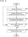
- FIG. 9 depicts a flowchart indicative of one example of the processing of receiving write data by the slave 13 illustrated in FIG. 1 .
- the processing starts and, upon receiving one word of the write data in step S21, the send/receive block 31 supplies the signal used for sending this write data to the recognition block 32.
- step S22 the recognition block 32 confirms the notification information included in the signal supplied from the 21 in step S21 so as to recognize whether this word has invalid data or not. For example, if a signal including the notification information indicative that the byte count of the valid is one byte is transferred in step S13 of FIG. 8 , then the recognition block 32 recognizes that the word has invalid data. On the other hand, if a signal including the notification information indicative the byte count of the valid data is two bytes in step S14 of FIG. 8 , then the recognition block 32 recognizes that the word does not have invalid data.
- step S23 on the basis of a result of the confirmation of the notification information by the recognition block 32 in step S22, the send/receive block 31 masks the invalid data included in the word having invalid data. That is, the send/receive block 31 extracts only the valid data from the word having invalid data and supplies the extracted valid data to the processing execution block 34.
- step S24 the send/receive block 31 determines whether the write data have all been received from the master 12.
- step S24 If the send/receive block 31 determines that the write data sent from the master 12 have not all been received in step S24, then the processing returns to step S21 to repeat the similar processing on the write data for one word to be sent next.
- step S24 if the send/receive block 31 determines that the write data sent from the master 12 have all been received in step S24, then the processing goes to step S25.
- step S25 the recognition block 32 obtains the byte count of the valid data of the entire write data on the basis of the byte count of the valid data of the write data per one word and the all sent word counts, upon which the processing is terminated.
- the presence or absence of invalid data can be recognized in the slave 13, so that the avoidance of the erroneous recognition between valid data and invalid data allows more correct communication.
- invalid data can be prevented from being written to an address not intended by a register, thereby allowing the correct writing of only the valid data to a register.
- the bus IF 11 if the byte count of the valid data of the write data per one word is sent, the data length of the valid data of the entire write data need not be separately sent, for example, thereby enhancing the efficiency of transmission. That is, the unnecessity of using a packet header and the like for transmitting data a data length allows the reduction of the data to be transmitted by that amount.
- the send/receive block 21, confirmation block 22, and the recognition block 23 in the master 12 and the send/receive block 31, the recognition block 32, and confirmation block 33 in the slave 13 are mounted on the physical layer.
- This setup makes it unnecessary to change the standard of the existing link layer necessary for providing a configuration in which to execute the rounding of the valid data on the upper link layer, for example.
- Changing the standard of the existing link layer as described above may cause a large influence due to the difference in the link layer standard between communication apparatuses; however, the occurrence of such an influence can be avoided in the bus IF 11.
- bus IF 11 compliant with the I3C standard and therefore applicable to the bus IF 11 compliant with other standards.
- FIG. 1 an example in which the slaves 13-1 through 13-3 are interconnected is illustrated; however, it is also practicable to provide onr or two or more than three units of the slave 13, for example.
- the slave 13 may be other than the memory or the register and the data to be sent by the master 12 to the slave 13 is not restricted to write data.
- the slave 13 is a device for controlling the light emission of a light-emitting element, then the data indicative of a timing of light-emitting a light-emitting element is sent from the master 12 and, on the basis of this data, the slave 13 can correctly make the light-emitting element emit light.
- processing operations described with reference to the flowchart described above need not always be sequentially executed in time series described in these flowcharts; namely, these processing operations include processing operations that are executed in parallel or discretely (parallel processing or processing based on objects, for example). Further, a program may be processed by one unit of CPU or by two or more units of CPU in a distributed manner.
- sequence of processing operations described above may be executed by hardware as well as software.
- the programs configuring this software are installed in a computer in which dedicated hardware containing these programs is built or a general-purpose personal computer, for example, in which various functions can be executed by installing various programs from a program recording medium to which the programs are recorded.
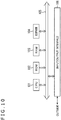
- FIG. 10 depicts a block diagram illustrating an example of the hardware of a computer in which the sequence of processing operations described above is executed by programs.
- a CPU Central Processing Unit
- ROM Read Only Memory
- RAM Random Access Memory
- EEPROM Electrically Erasable and Programmable Read Only Memory
- the bus 105 is further connected to an input/output interface 106 that is connected to the outside (the data signal line 14-1 and the clock signal line 14-2 illustrated in FIG. 1 , for example).
- the CPU 101 loads programs from the ROM 102 and EEPROM 104, for example, into the RAM 103 via the bus 105 and executes the loaded programs, thereby executing the sequence of processing operations described above. Also, in addition for the programs to be executed by the computer (the CPU 101) to be written to the ROM 102 in advance, these programs can be installed into the EEPROM 104 from the outside via the input/output interface 106 for execution or updating.
Landscapes
- Engineering & Computer Science (AREA)
- Theoretical Computer Science (AREA)
- General Engineering & Computer Science (AREA)
- Physics & Mathematics (AREA)
- General Physics & Mathematics (AREA)
- Computer Networks & Wireless Communication (AREA)
- Signal Processing (AREA)
- Computer Security & Cryptography (AREA)
- Quality & Reliability (AREA)
- Communication Control (AREA)
- Bus Control (AREA)
- Information Transfer Systems (AREA)
Applications Claiming Priority (2)
| Application Number | Priority Date | Filing Date | Title |
|---|---|---|---|
| JP2015244900 | 2015-12-16 | ||
| PCT/JP2016/085858 WO2017104440A1 (fr) | 2015-12-16 | 2016-12-02 | Dispositif de communication, procédé de communication, programme, et système de communication |
Publications (2)
| Publication Number | Publication Date |
|---|---|
| EP3392778A1 true EP3392778A1 (fr) | 2018-10-24 |
| EP3392778A4 EP3392778A4 (fr) | 2019-01-09 |
Family
ID=59056374
Family Applications (1)
| Application Number | Title | Priority Date | Filing Date |
|---|---|---|---|
| EP16875423.2A Withdrawn EP3392778A4 (fr) | 2015-12-16 | 2016-12-02 | Dispositif de communication, procédé de communication, programme, et système de communication |
Country Status (6)
| Country | Link |
|---|---|
| US (1) | US20180322084A1 (fr) |
| EP (1) | EP3392778A4 (fr) |
| JP (1) | JPWO2017104440A1 (fr) |
| KR (1) | KR20180096580A (fr) |
| CN (1) | CN108369568A (fr) |
| WO (1) | WO2017104440A1 (fr) |
Families Citing this family (2)
| Publication number | Priority date | Publication date | Assignee | Title |
|---|---|---|---|---|
| CN109144913A (zh) * | 2018-09-29 | 2019-01-04 | 联想(北京)有限公司 | 一种数据处理方法、系统及电子设备 |
| CN113283215B (zh) * | 2021-07-15 | 2021-12-10 | 北京华云安信息技术有限公司 | 一种基于utf-32编码的数据混淆方法及装置 |
Family Cites Families (7)
| Publication number | Priority date | Publication date | Assignee | Title |
|---|---|---|---|---|
| JP3613865B2 (ja) * | 1995-12-07 | 2005-01-26 | ソニー株式会社 | 電子機器及び通信制御方法 |
| US6356984B1 (en) | 1998-06-30 | 2002-03-12 | Sun Microsystems, Inc. | Digital data processing system having a data bus and a control bus |
| US6874052B1 (en) | 2000-09-29 | 2005-03-29 | Lucent Technologies Inc. | Expansion bridge apparatus and method for an I2C bus |
| US7068673B2 (en) * | 2002-02-27 | 2006-06-27 | Annadurai Andy P | Circuit and method for processing communication packets and valid data bytes |
| JP2003271549A (ja) * | 2002-03-19 | 2003-09-26 | Hitachi Ltd | 通信制御用半導体集積回路 |
| US8196009B2 (en) * | 2008-06-18 | 2012-06-05 | Intel Corporation | Systems, methods, and apparatuses to transfer data and data mask bits in a common frame with a shared error bit code |
| US8970750B2 (en) * | 2010-11-12 | 2015-03-03 | Sony Corporation | Image outputting apparatus, image outputting method, image processing apparatus, image processing method, program, data structure and imaging apparatus |
-
2016
- 2016-12-02 EP EP16875423.2A patent/EP3392778A4/fr not_active Withdrawn
- 2016-12-02 JP JP2017555977A patent/JPWO2017104440A1/ja not_active Abandoned
- 2016-12-02 KR KR1020187013006A patent/KR20180096580A/ko not_active Withdrawn
- 2016-12-02 US US15/773,089 patent/US20180322084A1/en not_active Abandoned
- 2016-12-02 WO PCT/JP2016/085858 patent/WO2017104440A1/fr not_active Ceased
- 2016-12-02 CN CN201680071827.9A patent/CN108369568A/zh not_active Withdrawn
Also Published As
| Publication number | Publication date |
|---|---|
| JPWO2017104440A1 (ja) | 2018-10-04 |
| WO2017104440A1 (fr) | 2017-06-22 |
| KR20180096580A (ko) | 2018-08-29 |
| US20180322084A1 (en) | 2018-11-08 |
| CN108369568A (zh) | 2018-08-03 |
| EP3392778A4 (fr) | 2019-01-09 |
Similar Documents
| Publication | Publication Date | Title |
|---|---|---|
| CN108139954B (zh) | 通信设备、通信方法、程序以及通信系统 | |
| US9798684B2 (en) | Bus communications with multi-device messaging | |
| US8464020B2 (en) | Non-volatile storage device, host device, storage system, data communication method and program | |
| EP3458962B1 (fr) | Dispositif de communication, et système de communication | |
| JP4966695B2 (ja) | マルチマスタのチェーン接続された二線シリアルバス装置及びディジタル状態機械 | |
| CN109154925B (zh) | 通信设备、通信方法、程序和通信系统 | |
| CN113722261A (zh) | Spi扩展片选数目和增强读写响应时间灵活性的方法 | |
| US6931468B2 (en) | Method and apparatus for addressing multiple devices simultaneously over a data bus | |
| EP3392778A1 (fr) | Dispositif de communication, procédé de communication, programme, et système de communication | |
| KR102298483B1 (ko) | 디지털 액세서리 인터페이스 | |
| CN109155689B (zh) | 通信设备、通信方法、程序和通信系统 | |
| US10824582B2 (en) | Communication apparatus, communication method, program, and communication system | |
| TW201606516A (zh) | 主機板組件及其資料處理系統 | |
| EP4530870A1 (fr) | Système et procédé de communication d'interface périphérique série | |
| CN106227682B (zh) | 电子装置、存储器装置及其数据交换方法 | |
| JP2018125814A (ja) | 伝送装置、伝送方法及び伝送システム | |
| JP6107499B2 (ja) | 通信制御装置及び画像形成装置 | |
| CN114911736A (zh) | 一种主从机系统 |
Legal Events
| Date | Code | Title | Description |
|---|---|---|---|
| PUAI | Public reference made under article 153(3) epc to a published international application that has entered the european phase |
Free format text: ORIGINAL CODE: 0009012 |
|
| 17P | Request for examination filed |
Effective date: 20180713 |
|
| AK | Designated contracting states |
Kind code of ref document: A1 Designated state(s): AL AT BE BG CH CY CZ DE DK EE ES FI FR GB GR HR HU IE IS IT LI LT LU LV MC MK MT NL NO PL PT RO RS SE SI SK SM TR |
|
| AX | Request for extension of the european patent |
Extension state: BA ME |
|
| A4 | Supplementary search report drawn up and despatched |
Effective date: 20181211 |
|
| RIC1 | Information provided on ipc code assigned before grant |
Ipc: H04L 29/06 20060101ALI20181205BHEP Ipc: G06F 13/42 20060101ALI20181205BHEP Ipc: G06F 13/38 20060101AFI20181205BHEP |
|
| DAV | Request for validation of the european patent (deleted) | ||
| DAX | Request for extension of the european patent (deleted) | ||
| 17Q | First examination report despatched |
Effective date: 20191002 |
|
| GRAP | Despatch of communication of intention to grant a patent |
Free format text: ORIGINAL CODE: EPIDOSNIGR1 |
|
| INTG | Intention to grant announced |
Effective date: 20200507 |
|
| STAA | Information on the status of an ep patent application or granted ep patent |
Free format text: STATUS: THE APPLICATION IS DEEMED TO BE WITHDRAWN |
|
| 18D | Application deemed to be withdrawn |
Effective date: 20200918 |